EP0732426B1 - Verfahren zur kontinuierlichen anodischen Oxidation von Bändern oder Drähten aus Aluminium - Google Patents
Verfahren zur kontinuierlichen anodischen Oxidation von Bändern oder Drähten aus Aluminium Download PDFInfo
- Publication number
- EP0732426B1 EP0732426B1 EP96810143A EP96810143A EP0732426B1 EP 0732426 B1 EP0732426 B1 EP 0732426B1 EP 96810143 A EP96810143 A EP 96810143A EP 96810143 A EP96810143 A EP 96810143A EP 0732426 B1 EP0732426 B1 EP 0732426B1
- Authority
- EP
- European Patent Office
- Prior art keywords
- oxide layer
- process according
- pore structure
- value
- anodising
- Prior art date
- Legal status (The legal status is an assumption and is not a legal conclusion. Google has not performed a legal analysis and makes no representation as to the accuracy of the status listed.)
- Expired - Lifetime
Links
Images


Classifications
-
- C—CHEMISTRY; METALLURGY
- C25—ELECTROLYTIC OR ELECTROPHORETIC PROCESSES; APPARATUS THEREFOR
- C25D—PROCESSES FOR THE ELECTROLYTIC OR ELECTROPHORETIC PRODUCTION OF COATINGS; ELECTROFORMING; APPARATUS THEREFOR
- C25D11/00—Electrolytic coating by surface reaction, i.e. forming conversion layers
- C25D11/02—Anodisation
- C25D11/04—Anodisation of aluminium or alloys based thereon
-
- C—CHEMISTRY; METALLURGY
- C25—ELECTROLYTIC OR ELECTROPHORETIC PROCESSES; APPARATUS THEREFOR
- C25D—PROCESSES FOR THE ELECTROLYTIC OR ELECTROPHORETIC PRODUCTION OF COATINGS; ELECTROFORMING; APPARATUS THEREFOR
- C25D11/00—Electrolytic coating by surface reaction, i.e. forming conversion layers
- C25D11/02—Anodisation
- C25D11/024—Anodisation under pulsed or modulated current or potential
-
- C—CHEMISTRY; METALLURGY
- C25—ELECTROLYTIC OR ELECTROPHORETIC PROCESSES; APPARATUS THEREFOR
- C25D—PROCESSES FOR THE ELECTROLYTIC OR ELECTROPHORETIC PRODUCTION OF COATINGS; ELECTROFORMING; APPARATUS THEREFOR
- C25D11/00—Electrolytic coating by surface reaction, i.e. forming conversion layers
- C25D11/02—Anodisation
- C25D11/04—Anodisation of aluminium or alloys based thereon
- C25D11/06—Anodisation of aluminium or alloys based thereon characterised by the electrolytes used
- C25D11/08—Anodisation of aluminium or alloys based thereon characterised by the electrolytes used containing inorganic acids
Definitions
- the invention relates to a method for producing a Oxide layer with pore structure on the surface of a tape or wire made of aluminum or an aluminum alloy by continuously passing the tape or wire through an electrolyte and simultaneous anodic oxidation the desired under pore-forming conditions Anodizing voltage generating layer thickness.
- the inventor has set himself the task of To create a method of the type mentioned, in which the thickness of the oxide layer is freely selectable regardless of the desired surface topography.
- the anodizing voltage in a first step to form a fine pore structure to a first value adjusted and then in a second step to form a coarser Pore structure continuously from the first value to that to achieve the desired one Layer thickness required final value increased and on this final value at least until the rate of formation and redissolution the oxide layer are the same size with a given throughput speed of the strip or wire through the electrolyte, the composition and the temperature of the electrolyte and the anodizing voltage be chosen or adjusted so that the balance between education and redissolving the oxide layer after a treatment period of 4 to 30 seconds and is achieved with a layer thickness between 250 and 1500 nm.
- stage 2 there is a reorganization of the pore structure, in technical jargon Called pore joining or pore union: the one formed during stage 2 Pore structure is coarser than the pore structure of stage 1.
- the further layer growth is due to the increased rate of education due to the higher Anodizing voltage guaranteed.
- the pores of the top become fine structured layer extended by redissolution. Due to the smaller one Pore spacing this pore expansion can progress until neighboring Pores on the surface of the oxide layer with the formation of claw-shaped oxide tips touch.
- the first value of the anodizing voltage is preferably between about 25 to 75%, especially around 50% of the final value.
- the anodizing voltage increases from the first value to the final value expediently relatively slow, preferably within about 2 to 3 seconds.
- a sudden increase in the anodizing voltage is not recommended because of a sudden reorganization of the pore structure embrittlement of the oxide layer could result in later delamination of the lacquered or glued tape cannot be excluded.
- the anodizing voltage after reaching of the first value without a hold time changes to the final value.
- the residence time on the final value of the anodizing voltage is preferably between about 25 and 75%, especially about 50%, of the total treatment time.
- Electrolyte contains phosphoric acid and / or sulfuric acid.
- the oxide layer produced according to the invention can be carried out in a known manner Impregnation with corrosion inhibitors, especially with chromates, phosphates or cerium salts.
- the oxide layer can also Hydration inhibitors, in particular with phosphates or phosphoric acid derivatives, be impregnated.
- FIG. 3 shows the time profile of the anodizing voltage when carrying out the method according to the invention.
- AB rapid increase
- the voltage of 25V is kept constant for 3 seconds (BC)
- CD 50V within 3 seconds
- DE depleted voltage
- EF EF
- the anodizing voltage can be a pronounced first holding stage (BC) also continuously from the first to the second level can be increased (BD).
- the duration of the second Treatment level (DE) depends on the desired layer thickness and the claw-shaped tip structure. Usually is the desired oxide layer after about 3 seconds educated. Of course there are many ways to generate the voltage curve shown.
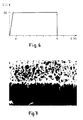
- Fig. 7 shows that with the method according to the prior art generated coarse-pore oxide layer.
Description
| Dicke der Sperrschicht | 10,4 Å/V |
| Zellendurchmesser A | 27,7 Å/V |
| Zellenwandstärke B | 7,4 Å/V |
| Porendurchmesser C | 12,9 Å/V |
| Porenabstand D | 14,8 Å/V |
- Stufe 1:
- Bildung einer feinen Porenstruktur durch anodische Oxidation bei niedriger Anodisierspannung, z.B. 25V/3s.
- Stufe 2:
- Fortführung der anodischen Oxidation bei erhöhter Anodisierspannung, z.B. 50V/3s.
- Fig. 1
- den Querschnitt durch zwei benachbarte Zellen einer Oxidschicht in schematischer Darstellung;
- Fig. 2
- die verschiedenen Stufen der Bildung und Rücklösung einer anodischen Oxidschicht in schematischer Darstellung;
- Fig. 3
- ein Beispiel für den zeitlichen Verlauf der Anodisierspannung;
- Fig. 4
- eine Raster-Elektronenmikroskop(REM)-Aufnahme der Bruchfläche einer nach dem erfindungsgemässen Verfahren hergestellten Oxidschicht (Vergrösse50'000x);
- Fig. 5
- eine REM-Aufnahme der Oberfläche einer nach dem erfindungsgemässen Verfahren hergestellten Oxidschicht (Vergrösserung 50'000x);
- Fig. 6
- den zeitlichen Verlauf der Anodisierspannung bei der Herstellung einer Oxidschicht mit einem Verfahren nach dem Stand der Technik;
- Fig. 7
- eine REM-Aufnahme der Bruchfläche einer nach dem zeitlichen Verlauf der Anodisierspannung nach Fig. 6 hergestellten Oxidschicht;
- Fig. 8
- den zeitlichen Verlauf der Anodisierspannung bei Durchführung des erfindungsgemässen Verfahrens;
- Fig. 9
- eine REM-Aufnahme der Bruchfläche einer nach dem zeitlichen Verlauf der Anodisierspannung nach Fig. 8 hergestellten Oxidschicht.
- Elektrolyt:
- H3PO4 / 150g/l / 65°C
- Bandgeschwindikeit:
- 30m/min
| Haftung Nmm/mm | |||
| Verbund | Anfangswert | Nach 1000 Std.ESS | Bruchbild |
| A | 120 | 125 | 100% Adhäsion |
| B | 413 | 394 | 50% Adhäsion |
| 50% Kohäsion | |||
| A Hergestellt mit Al-Band aus Beispiel 1 | |||
| B Hergestellt mit Al-Band aus Beispiel 2 |
Claims (9)
- Verfahren zur Herstellung einer Oxidschicht mit Porenstruktur auf der Oberfläche eines Bandes oder Drahtes aus Aluminium oder einer Aluminiumlegierung durch kontinuierliche Durchführung des Bandes oder Drahtes durch einen Elektrolyten und gleichzeitige anodische Oxidation unter porenbildenden Bedingungen bei einer die gewünschte Schichtdicke erzeugenden Anodisierspannung,
dadurch gekennzeichnet,
dass die Anodisierspannung in einem ersten Schritt zur Bildung einer feinen Porenstruktur auf einen ersten Wert (U1) eingestellt und nachfolgend in einem zweiten Schritt zur Bildung einer gröberen Porenstruktur kontinuierlich vom ersten Wert (U1) auf den zum Erreichen der gewünschten Schichtdicke erforderlichen Endwert (U2) erhöht und auf diesem Endwert (U2) zumindest solange gehalten wird, bis die Bildungs- und Rücklösungsgeschwindigkeit der Oxidschicht gleich gross sind, wobei bei vorgegebener Durchlaufgeschwindigkeit des Bandes bzw. des Drahtes durch den Elektrolyten die Zusammensetzung und die Temperatur des Elektrolyten sowie die Anodisierspannung derart gewählt bzw. eingestellt werden, dass das Gleichgewicht zwischen Bildung und Rücklösung der Oxidschicht nach einer Behandlungsdauer von 4 bis 30 Sekunden und bei einer Schichtdicke zwischen 250 und 1500 nm erreicht wird. - Verfahren nach Anspruch 1, dadurch gekennzeichnet, dass der erste Wert (U1) der Anodisierspannung 25 bis 75%, vorzugsweise etwa 50%, vom Endwert (U2) beträgt.
- Verfahren nach Anspruch 1 oder 2, dadurch gekennzeichnet, dass der Anstieg der Anodisierspannung vom ersten Wert (U1) auf den Endwert (U2) verhältnismässig langsam, vorzugsweise innerhalb von 2 bis 3 Sekunden, erfolgt.
- Verfahren nach einem der Ansprüche 1 bis 3, dadurch gekennzeichnet, dass die Verweildauer auf dem Endwert (U2) der Anodisierspannung 25 bis 75%, vorzugsweise etwa 50%, von der gesamten Behandlungsdauer beträgt.
- Verfahren nach einem der Ansprüche 1 bis 4, dadurch gekennzeichnet, dass die anodische Oxidation mit Gleichstrom durchgeführt wird.
- Verfahren nach einem der Ansprüche 1 bis 5, dadurch gekennzeichnet, dass der Elektrolyt Phosphorsäure und/ oder Schwefelsäure enthält.
- Verfahren nach einem der Ansprüche 1 bis 6, dadurch gekennzeichnet, dass die Oxidschicht durch Imprägnieren mit Korrosionsinhibitoren, insbesondere mit Chromaten, Phosphaten oder Ceriumsalzen, nachbehandelt wird.
- Verfahren nach einem der Ansprüche 1 bis 7, dadurch gekennzeichnet, däss die Oxidschicht durch Imprägnieren mit Hydratationsinhibitoren, insbesondere mit Phosphaten oder Phosphorsäurederivaten, nachbehandelt wird.
- Verwendung des Verfahrens nach einem der Ansprüche 1 bis 8 zur Herstellung einer Oxidschicht mit einer Porenstruktur enthaltend Oxidspitzen, insbesondere pyramiden- oder krallenartige Oxidspitzen, als Verankerungspunkte für einen nachträglich aufgebrachten Klebstoff oder Lack.
Applications Claiming Priority (3)
| Application Number | Priority Date | Filing Date | Title |
|---|---|---|---|
| CH74995 | 1995-03-16 | ||
| CH749/95 | 1995-03-16 | ||
| CH00749/95A CH689395A5 (de) | 1995-03-16 | 1995-03-16 | Verfahren zur kontinuierlichen anodischen Oxidation von Baendern oder Draehten aus Aluminium. |
Publications (2)
| Publication Number | Publication Date |
|---|---|
| EP0732426A1 EP0732426A1 (de) | 1996-09-18 |
| EP0732426B1 true EP0732426B1 (de) | 2000-02-02 |
Family
ID=4194309
Family Applications (1)
| Application Number | Title | Priority Date | Filing Date |
|---|---|---|---|
| EP96810143A Expired - Lifetime EP0732426B1 (de) | 1995-03-16 | 1996-03-08 | Verfahren zur kontinuierlichen anodischen Oxidation von Bändern oder Drähten aus Aluminium |
Country Status (4)
| Country | Link |
|---|---|
| US (1) | US5693208A (de) |
| EP (1) | EP0732426B1 (de) |
| CH (1) | CH689395A5 (de) |
| DE (1) | DE59604337D1 (de) |
Families Citing this family (23)
| Publication number | Priority date | Publication date | Assignee | Title |
|---|---|---|---|---|
| US6810575B1 (en) * | 1998-04-30 | 2004-11-02 | Asahi Kasai Chemicals Corporation | Functional element for electric, electronic or optical device and method for manufacturing the same |
| DE10154756C1 (de) * | 2001-07-02 | 2002-11-21 | Alcove Surfaces Gmbh | Verwendung einer anodisch oxidierten Oberflächenschicht |
| DE10020877C1 (de) * | 2000-04-28 | 2001-10-25 | Alcove Surfaces Gmbh | Prägewerkzeug, Verfahren zum Herstellen desselben, Verfahren zur Strukturierung einer Oberfläche eines Werkstücks und Verwendung einer anodisch oxidierten Oberflächenschicht |
| US7066234B2 (en) | 2001-04-25 | 2006-06-27 | Alcove Surfaces Gmbh | Stamping tool, casting mold and methods for structuring a surface of a work piece |
| FR2812968B1 (fr) * | 2000-08-11 | 2003-08-01 | Thomson Csf | Capteur micro-usine avec protection isolante des connexions |
| FR2812969B1 (fr) * | 2000-08-11 | 2003-08-01 | Thomson Csf | Capteur micro-usine avec soudure electrolytique et procede de fabrication |
| US7274463B2 (en) * | 2003-12-30 | 2007-09-25 | Sensory Analytics | Anodizing system with a coating thickness monitor and an anodized product |
| US7365860B2 (en) * | 2000-12-21 | 2008-04-29 | Sensory Analytics | System capable of determining applied and anodized coating thickness of a coated-anodized product |
| US6674533B2 (en) | 2000-12-21 | 2004-01-06 | Joseph K. Price | Anodizing system with a coating thickness monitor and an anodized product |
| WO2007103304A2 (en) * | 2006-03-07 | 2007-09-13 | Sensory Analytics | A mobile apparatus capable of surface measurements of a coating thickness |
| US8609254B2 (en) | 2010-05-19 | 2013-12-17 | Sanford Process Corporation | Microcrystalline anodic coatings and related methods therefor |
| US8512872B2 (en) | 2010-05-19 | 2013-08-20 | Dupalectpa-CHN, LLC | Sealed anodic coatings |
| US8572838B2 (en) | 2011-03-02 | 2013-11-05 | Honeywell International Inc. | Methods for fabricating high temperature electromagnetic coil assemblies |
| US8466767B2 (en) | 2011-07-20 | 2013-06-18 | Honeywell International Inc. | Electromagnetic coil assemblies having tapered crimp joints and methods for the production thereof |
| US8860541B2 (en) | 2011-10-18 | 2014-10-14 | Honeywell International Inc. | Electromagnetic coil assemblies having braided lead wires and methods for the manufacture thereof |
| US9076581B2 (en) | 2012-04-30 | 2015-07-07 | Honeywell International Inc. | Method for manufacturing high temperature electromagnetic coil assemblies including brazed braided lead wires |
| US8754735B2 (en) | 2012-04-30 | 2014-06-17 | Honeywell International Inc. | High temperature electromagnetic coil assemblies including braided lead wires and methods for the fabrication thereof |
| DE102012019969A1 (de) * | 2012-10-08 | 2014-04-24 | Hans und Ottmar Binder GbR (vertretungsberechtigte Gesellschafter: Hans Binder, 89558 Böhmenkirch; Ottmar Binder, 89558 Böhmenkirch) | Verfahren zum Herstellen einer Sol-Gel-Beschichtung auf einer zu beschichtenden Oberfläche eines Bauteils sowie entsprechendes Bauteil |
| EP2904132A1 (de) * | 2012-10-08 | 2015-08-12 | Süddeutsche Aluminium Manufaktur GmbH | Verfahren zum herstellen einer sol-gel-beschichtung auf einer zu beschichtenden oberfläche eines bauteils sowie entsprechendes bauteil |
| US9818501B2 (en) | 2012-10-18 | 2017-11-14 | Ford Global Technologies, Llc | Multi-coated anodized wire and method of making same |
| US9027228B2 (en) | 2012-11-29 | 2015-05-12 | Honeywell International Inc. | Method for manufacturing electromagnetic coil assemblies |
| US9722464B2 (en) | 2013-03-13 | 2017-08-01 | Honeywell International Inc. | Gas turbine engine actuation systems including high temperature actuators and methods for the manufacture thereof |
| CN111139510B (zh) * | 2020-01-15 | 2021-01-19 | 大连海事大学 | 一种船用低碳钢防腐涂层的制备方法 |
Family Cites Families (13)
| Publication number | Priority date | Publication date | Assignee | Title |
|---|---|---|---|---|
| DE235081C (de) * | 1900-01-01 | |||
| GB223994A (en) * | 1923-08-02 | 1924-11-03 | Guy Dunstan Bengough | Improved process of protecting surfaces of aluminium of aluminium alloys |
| GB387437A (en) * | 1930-11-08 | 1933-02-09 | Andre Albert Samuel | Process of manufacture of thin solid films, insulating and having a high dielectric strength |
| US3020219A (en) * | 1959-01-12 | 1962-02-06 | Electralab Printed Electronics | Process for producing oxide coatings on high silicon aluminum alloy |
| FR1486833A (fr) * | 1965-07-16 | 1967-06-30 | Becromal Spa | Procédé pour la formation des électrodes pour condensateurs électrolytiques |
| NL6612707A (de) * | 1966-09-09 | 1968-03-11 | ||
| JPS582486B2 (ja) * | 1973-05-11 | 1983-01-17 | 富士通株式会社 | タイマ− |
| LU80237A1 (fr) * | 1978-09-14 | 1980-04-21 | Brevelco Sa | Procede d'anodisation dure de l'aluminium et des alliages d'aluminium et produits obtenus par ce procede |
| DE3312497A1 (de) * | 1983-04-07 | 1984-10-11 | Hoechst Ag, 6230 Frankfurt | Zweistufiges verfahren zur herstellung von anodisch oxidierten flaechigen materialien aus aluminium und deren verwendung bei der herstellung von offsetdruckplatten |
| NL8600207A (nl) * | 1986-01-29 | 1987-08-17 | Fokker Bv | Chroomzuur/fosforzuur-anodiseerproces voor oppervlaktebehandeling van lichtmetaal. |
| JP2663544B2 (ja) * | 1988-08-24 | 1997-10-15 | 松下電器産業株式会社 | アルミニウム電解コンデンサ用電極箔の製造方法 |
| FR2684393B1 (fr) * | 1991-11-29 | 1994-12-09 | Dassault Aviat | Procede de colmatage d'une couche d'anodisation obtenue en bain chromique. |
| US5566952A (en) * | 1996-01-24 | 1996-10-22 | Moving Target Sports, Inc. | Foldable sports goal structure |
-
1995
- 1995-03-16 CH CH00749/95A patent/CH689395A5/de not_active IP Right Cessation
-
1996
- 1996-03-05 US US08/599,360 patent/US5693208A/en not_active Expired - Lifetime
- 1996-03-08 EP EP96810143A patent/EP0732426B1/de not_active Expired - Lifetime
- 1996-03-08 DE DE59604337T patent/DE59604337D1/de not_active Expired - Lifetime
Also Published As
| Publication number | Publication date |
|---|---|
| US5693208A (en) | 1997-12-02 |
| DE59604337D1 (de) | 2000-03-09 |
| EP0732426A1 (de) | 1996-09-18 |
| CH689395A5 (de) | 1999-03-31 |
Similar Documents
| Publication | Publication Date | Title |
|---|---|---|
| EP0732426B1 (de) | Verfahren zur kontinuierlichen anodischen Oxidation von Bändern oder Drähten aus Aluminium | |
| DE2462449A1 (de) | Verfahren zum kontinuierlichen elektrolytischen eloxieren und galvanisieren von aluminium sowie vorrichtung zur durchfuehrung dieses verfahrens | |
| DE102004041813A1 (de) | Oberfläche mit einer haftungsvermindernden Mikrostruktur und Verfahren zu deren Herstellung | |
| EP2238280B1 (de) | Multifunktionelle beschichtung von aluminiumteilen | |
| DE2800258A1 (de) | Verfahren zur erzeugung zinkhaltiger mehrfachueberzuege | |
| WO1998009764A1 (de) | Hochfeste erodierelektrode | |
| EP3594969A1 (de) | Verfahren zur herstellung eines mit elektroisolierlack beschichteten leiterdrahtes und elektroisolierlack | |
| EP1743053B1 (de) | Verfahren zur herstellung einer beschichtung | |
| EP0761844A1 (de) | Verfahren zur galvanischen Verchromung | |
| DE102012213455B4 (de) | Verfahren zur Bildung einer Korrosionsschutzschicht an der Oberfläche eines CFK-Bauteils | |
| DE102009028136B3 (de) | Gleitlagerverbundwerkstoff, Gleitlagerelement und Verfahren zu deren Herstellung | |
| DE2243178A1 (de) | Verfahren zur bildung eines harten anodischen oxydfilmes auf einer aluminiumlegierung | |
| EP4035788A1 (de) | Verfahren zum texturieren einer dressierwalze, dressierwalze und dressiertes stahlblech | |
| DE4432512C2 (de) | Verwendung eines Verfahrens zur elektrolytischen Abscheidung von Chromschichten | |
| DE1496752A1 (de) | Anodisches Bad | |
| DE4429936A1 (de) | Vorbereitung von Metalloberflächen für das Emaillieren | |
| DE4213535C1 (en) | Anodising aluminium@ and magnesium@ surfaces - by constantly increasing current to predetermined max. value and holding at this value so that ratio of charge in 1st stage to 2nd stage is approximately 0.5 | |
| DE2609577A1 (de) | Verfahren zur erzeugung versiegelter anodischer oxidduennschichten auf aluminium und aluminiumlegierungen vor deren beschichtung | |
| DE2528143C3 (de) | Kaltgewalztes Emaillierstahlblech | |
| DE2402653A1 (de) | Armierteil fuer mauerwerk und herstellungsverfahren dafuer | |
| DE1954641A1 (de) | Verfahren zum Herstellen eines metallischen Laminats | |
| DE4243164A1 (de) | Verfahren zur anodischen Oxidation | |
| DE3225083A1 (de) | Verfahren zur anodischen behandlung einer verzinnten metalloberflaeche | |
| DE965715C (de) | Verfahren zum Schutze von Aluminium oder Aluminiumlegierungen vor Korrosion | |
| EP0355272B1 (de) | Für die Aussenseite von Kraftfahrzeugkarosserieteilen bestimmtes mehrfach beschichtetes Stahlblech |
Legal Events
| Date | Code | Title | Description |
|---|---|---|---|
| PUAI | Public reference made under article 153(3) epc to a published international application that has entered the european phase |
Free format text: ORIGINAL CODE: 0009012 |
|
| AK | Designated contracting states |
Kind code of ref document: A1 Designated state(s): CH DE FR IT LI NL |
|
| RAP1 | Party data changed (applicant data changed or rights of an application transferred) |
Owner name: ALUSUISSE TECHNOLOGY & MANAGEMENT AG |
|
| 17P | Request for examination filed |
Effective date: 19970318 |
|
| 17Q | First examination report despatched |
Effective date: 19980730 |
|
| GRAG | Despatch of communication of intention to grant |
Free format text: ORIGINAL CODE: EPIDOS AGRA |
|
| GRAG | Despatch of communication of intention to grant |
Free format text: ORIGINAL CODE: EPIDOS AGRA |
|
| GRAG | Despatch of communication of intention to grant |
Free format text: ORIGINAL CODE: EPIDOS AGRA |
|
| GRAH | Despatch of communication of intention to grant a patent |
Free format text: ORIGINAL CODE: EPIDOS IGRA |
|
| ITF | It: translation for a ep patent filed |
Owner name: DE DOMINICIS & MAYER S.R.L. |
|
| GRAH | Despatch of communication of intention to grant a patent |
Free format text: ORIGINAL CODE: EPIDOS IGRA |
|
| GRAA | (expected) grant |
Free format text: ORIGINAL CODE: 0009210 |
|
| AK | Designated contracting states |
Kind code of ref document: B1 Designated state(s): CH DE FR IT LI NL |
|
| REG | Reference to a national code |
Ref country code: CH Ref legal event code: EP |
|
| REF | Corresponds to: |
Ref document number: 59604337 Country of ref document: DE Date of ref document: 20000309 |
|
| ET | Fr: translation filed | ||
| PLBE | No opposition filed within time limit |
Free format text: ORIGINAL CODE: 0009261 |
|
| STAA | Information on the status of an ep patent application or granted ep patent |
Free format text: STATUS: NO OPPOSITION FILED WITHIN TIME LIMIT |
|
| 26N | No opposition filed | ||
| PGFP | Annual fee paid to national office [announced via postgrant information from national office to epo] |
Ref country code: CH Payment date: 20100325 Year of fee payment: 15 |
|
| PGFP | Annual fee paid to national office [announced via postgrant information from national office to epo] |
Ref country code: FR Payment date: 20100406 Year of fee payment: 15 |
|
| REG | Reference to a national code |
Ref country code: NL Ref legal event code: TD Effective date: 20100521 |
|
| PGFP | Annual fee paid to national office [announced via postgrant information from national office to epo] |
Ref country code: NL Payment date: 20100324 Year of fee payment: 15 Ref country code: IT Payment date: 20100330 Year of fee payment: 15 Ref country code: DE Payment date: 20100329 Year of fee payment: 15 |
|
| REG | Reference to a national code |
Ref country code: FR Ref legal event code: CD |
|
| REG | Reference to a national code |
Ref country code: NL Ref legal event code: V1 Effective date: 20111001 |
|
| REG | Reference to a national code |
Ref country code: CH Ref legal event code: PL |
|
| REG | Reference to a national code |
Ref country code: FR Ref legal event code: ST Effective date: 20111130 |
|
| PG25 | Lapsed in a contracting state [announced via postgrant information from national office to epo] |
Ref country code: DE Free format text: LAPSE BECAUSE OF NON-PAYMENT OF DUE FEES Effective date: 20111001 Ref country code: CH Free format text: LAPSE BECAUSE OF NON-PAYMENT OF DUE FEES Effective date: 20110331 Ref country code: LI Free format text: LAPSE BECAUSE OF NON-PAYMENT OF DUE FEES Effective date: 20110331 Ref country code: FR Free format text: LAPSE BECAUSE OF NON-PAYMENT OF DUE FEES Effective date: 20110331 Ref country code: NL Free format text: LAPSE BECAUSE OF NON-PAYMENT OF DUE FEES Effective date: 20111001 |
|
| REG | Reference to a national code |
Ref country code: DE Ref legal event code: R119 Ref document number: 59604337 Country of ref document: DE Effective date: 20111001 |
|
| PG25 | Lapsed in a contracting state [announced via postgrant information from national office to epo] |
Ref country code: IT Free format text: LAPSE BECAUSE OF NON-PAYMENT OF DUE FEES Effective date: 20110308 |