EP0735481B1 - System level mechanism for invalidating data stored in the external cache of a processor in a computer system - Google Patents
System level mechanism for invalidating data stored in the external cache of a processor in a computer system Download PDFInfo
- Publication number
- EP0735481B1 EP0735481B1 EP96301804A EP96301804A EP0735481B1 EP 0735481 B1 EP0735481 B1 EP 0735481B1 EP 96301804 A EP96301804 A EP 96301804A EP 96301804 A EP96301804 A EP 96301804A EP 0735481 B1 EP0735481 B1 EP 0735481B1
- Authority
- EP
- European Patent Office
- Prior art keywords
- memory
- subsystem
- processor
- external cache
- data block
- Prior art date
- Legal status (The legal status is an assumption and is not a legal conclusion. Google has not performed a legal analysis and makes no representation as to the accuracy of the status listed.)
- Expired - Lifetime
Links
Images


Classifications
-
- G—PHYSICS
- G06—COMPUTING; CALCULATING OR COUNTING
- G06F—ELECTRIC DIGITAL DATA PROCESSING
- G06F12/00—Accessing, addressing or allocating within memory systems or architectures
- G06F12/02—Addressing or allocation; Relocation
- G06F12/08—Addressing or allocation; Relocation in hierarchically structured memory systems, e.g. virtual memory systems
- G06F12/0802—Addressing of a memory level in which the access to the desired data or data block requires associative addressing means, e.g. caches
- G06F12/0806—Multiuser, multiprocessor or multiprocessing cache systems
- G06F12/0808—Multiuser, multiprocessor or multiprocessing cache systems with cache invalidating means
-
- G—PHYSICS
- G06—COMPUTING; CALCULATING OR COUNTING
- G06F—ELECTRIC DIGITAL DATA PROCESSING
- G06F12/00—Accessing, addressing or allocating within memory systems or architectures
- G06F12/02—Addressing or allocation; Relocation
- G06F12/08—Addressing or allocation; Relocation in hierarchically structured memory systems, e.g. virtual memory systems
- G06F12/0802—Addressing of a memory level in which the access to the desired data or data block requires associative addressing means, e.g. caches
- G06F12/0806—Multiuser, multiprocessor or multiprocessing cache systems
- G06F12/0815—Cache consistency protocols
- G06F12/0817—Cache consistency protocols using directory methods
Definitions
- the present invention pertains to the field of computer systems. More particularly, this invention relates to a computer system that includes a system level mechanism for invalidating data stored in the external cache of a processor in the computer system.
- Prior computer systems typically include one or more processor subsystems and one or more input/output subsystems coupled to a main memory subsystem.
- a main memory subsystem typically provides storage areas for instructions and data for the processors, as well as storage areas for data transfer to and from input/output devices coupled to the input/output subsystem.
- the processor subsystems and the input/output subsystems are coupled to the main memory subsystem via a physical interconnect that provides a common bus or a switched interconnect data path.
- a processor subsystem in such a system typically includes an associated external cache memory.
- Such an external cache memory usually stores selected blocks from the main memory subsystem.
- An external cache memory usually provides fast processor access to code and data by avoiding external fetches to the main memory subsystem for datablocks that are stored in the cache.
- such a computer system typically implements a protocol for maintaining data coherency between the main memory and the corresponding datablocks in the external cache memory.
- each external cache memory typically includes a set of tags that indicate the validity status of the datablocks stored in the external cache.
- such a computer system provides a mechanism for performing coherent data input/output.
- an input/output subsystem in such a computer system commonly injects new data into the system by issuing write invalidate (WRI) operations to the main memory subsystem.
- WRI write invalidate
- Such write invalidate operations may occur, for example, when a new page of data is read from a disk device coupled to the input/output subsystem.
- a processor subsystem commonly injects new data into the computer system using WRI operations during block copy operations.
- Such block copy operations occur, for example, during data structure initialization or during file copy operations in the computer system.
- Such block copy operations occur at a relatively high rate in a typical prior computer system.
- Such WRI operations usually require the invalidation of corresponding data blocks stored in an external processor caches to maintain data coherency in the system.
- Such an invalidate operation on an external cache is only necessary when the tags for that external cache indicate that the newly injected datablock is present.
- such an invalidation operation is performed within each processor subsystem.
- a processor reads the corresponding external tags to determine whether an invalidate operation is required during a write invalidate transaction.
- a tag read operation and potentially a tag read-modify-write operation for each WRI operation issued to the memory subsystem.
- WRI operations occur at a frequent rate in typical prior systems and interfere with normal instruction execution by the processors, thereby slowing the overall performance of such a system.
- processor subsystems that perform such self-invalidation operations may be incompatible with systems that provide directory based tags in the memory subsystem.
- Some computer systems may implement a worst case approach to such invalidate operations. For example, a system may blindly perform an external cache invalidate operation for every write invalidate transaction whether or not the datablock specified by the write invalidate transaction is present in the external cache. Such an invalidate operation is unnecessary whenever the specified datablock is not stored in the external cache. Unfortunately, such unnecessary invalidate operations interfere with normal operations of the processor.
- invalidate operations may be required during some types block copy operations while not during other types of block copy operations.
- a processor subsystem may require an invalidate operation during block copy operations that generate new memory datablocks that the processor subsystem will not later access.
- block copy operations that write datablocks to stable storage in the computer system typically do not require an invalidate operation to the external cache if the processor retains control over the datablocks transferred to stable storage.
- Prior systems that blindly perform invalidate operations usually cause the processor subsystem to later perform an external fetch to the memory subsystem for the specified datablocks. Unfortunately, such unnecessary external fetches to the memory subsystem slows the overall throughput of such a computer system.
- the invention consists in a computer system comprising a processor subsystem having an external cache memory; and a memory subsystem coupled to the processor subsystem, the memory subsystem being separate from the processor subsystem, the processor subsystem issuing a write invalidate (WRI) operation specifying a data block to be stored in memory subsystem, characterised in that the WRI operation includes an invalidate advisory (IVA) indication that indicates to the memory whether the data block is present in the external cache, the IVA indication determining whether the memory subsystem, in response to receiving the WRI operation, sends a message to said processor subsystem to invalidate the data block, and the method of operating the computer system.
- WRI write invalidate
- IVVA invalidate advisory
- the invention consists in a computer system comprising: a processor subsystem having an external cache memory and associated cache tags; and a memory interconnect including a mechanism for invalidating a data block in the external cache memory, the memory interconnect further being separate from the processor subsystem, wherein the memory interconnect invalidates the data block in response to an invalidate advisory (IVA) indication included in a write invalidate (WRI) operation issued by the processor subsystem that specifies the data block.
- IVA invalidate advisory
- WRI write invalidate
- the invention consists in a method for transferring a method for transferring data to a memory interconnect, the memory interconnect being separate from but coupled to a processor subsystem, the processor subsystem including an external cache memory, the method comprising the steps of: determining whether a data block is present in the external cache memory; issuing a write invalidate (WRI) operation specifying the data block to be stored in the memory interconnect, wherein the WRI operation further includes an invalidate advisory (IVA) indication that indicates to the memory interconnect whether the data block is present in the external cache memory; and invalidating the data block in response to detecting the IVA indication.
- WRI write invalidate
- IVVA invalidate advisory
- the mechanism in the memory subsystem or memory interconnect for invalidating the external cache of the processor simplifies the design of the processor to external cache interface and reduces the impact on processor performance of write invalidate operations in the system.
- Such an external mechanism for cache invalidation also eliminates read-modify-write operations by the processor to the external cache during write invalidate operations that would otherwise impact processor performance.
- such an external mechanism for cache invalidation provides a processor subsystem that is compatible with multiprocessor systems that maintain directory based or duplicate tags and with uniprocessor systems that do not maintain directory based or duplicate tags.
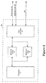
- Figure 1 illustrates a computer system 10 for one embodiment.
- the computer system 10 comprises a processor subsystem 10, and an input/output port 22, and a memory interconnect subsystem 18.
- the memory interconnect subsystem 18 provides shared access to a main memory 14 to the processor subsystem 20 and the input/output subsystem 22.
- Elements of the computer system 10 communicate with the memory interconnect subsystem 18 via a set of memory ports 1-N.
- port 1 for the processor subsystem 20 comprises a data path 40, an address path 42, and a control path 44
- port N for the input/output subsystem 22 comprises a data path 46, an address path 48 and a control path 50.
- the memory interconnect subsystem 18 includes a data path switch 12 to the main memory 14, and a system controller 16.
- the data path switch 12 is a cross bar switch controlled by the system controller 16 via a set of control signals 54.
- the data path switch 12 enables data path access to the main memory 14 via the data path of each port 1-N including the data path 40 and the data path 46.
- the system controller 16 functions as a memory controller by decoding the addresses received from the processor subsystems and I/O subsystem 20-22 and by generating memory control signals including row address select (RAS) and column address select (CAS) signals to the main memory 14 via a memory control bus 56.
- RAS row address select
- CAS column address select
- the system controller 16 receives memory access requests from the subsystems 20-22 via the address path of each port 1-N including the address path 42 and the address path 48.
- the system controller 16 arbitrates among the requests from the subsystems 20-22 and configures the data path switch 12 to provide the necessary connections for access to the main memory 14 via a memory data bus 52 or for subsystem to subsystem data transfers.
- the system controller 16 responds with cache state transition control messages to the processor subsystem 20 when necessary.
- the memory access requests include, for example, write invalidate (WRI) requests.
- WRI write invalidate
- the subsystems 20-22 use a WRI request to the system controller 16 to write a specified datablock into the main memory 14.
- the system controller 16 processes a WRI request by configuring the data path switch 12 to provide the proper source for the specified datablock. If the WRI request originates with the processor subsystem 20, then the system controller 16 transfers messages via the control path 44 to control the cache state transitions in the external cache of the processor subsystem 20. For example, the system controller 16 transfers invalidate messages via the control path 44 to invalidate datablocks in the external cache of the processor subsystem 20 when appropriate.
- system controller 16 maintains a set of duplicate tags that correspond to the external tags.
- system controller 16 accesses the duplicate tags via a snoop bus coupled between the system controller 16 and the duplicate tags.
- a snoop bus coupled between the system controller 16 and the duplicate tags.
- the input/output port 22 enables communication with a set of peripheral devices 30-33 via a standardized input/output bus 58.
- the standardized input/output bus 58 may comprise, for example, a SBUS or a peripheral component interconnect (PCI) standardized bus.
- the input/output port 22 implements a direct memory access mechanism that provides coherent input/output operations to the main memory 14 through the system controller 16.
- FIG. 2 illustrates the processor subsystem 20 for one embodiment.
- the processor subsystem 20 comprises a processor 70, an external cache 74, and an associated set of external tags 76 along with a port interface 72.
- the processor 70 issues memory load and memory store operations to the external cache 74.
- the port interface 72 issues a cache requests to the system controller 16 using a message packet transferred via the address pass 42.
- the cache requests include WRI transactions during block copy operations by the processor 70.
- Each message packet transferred via the address pass 42 includes a header that specifies the write invalidate request type along with an address that specifies the datablock for the write invalidate transaction.
- the system controller 16 processes a write invalidate transaction by configuring the datapath switch 12 to transfer the corresponding datablock to the main memory 14.
- the WRI request packet to the system controller 16 includes an invalidate advisory (IVA) indication.
- the IVA indication determines whether the system controller 16 issues an invalidate request back to the processor subsystem 20 to invalidate the corresponding datablock in the external cache 74.
- the processor subsystem 20 performs a copyback operation to the memory interconnect subsystem 18 in response to the invalidate request if the specified invalidated datablock is present in the external cache 74.
- FIG. 3 illustrates the input/output port 22 for one embodiment.
- the input/output port 22 comprises a standard input/output bus interface 80 along with a port interface 82.
- the port interface 82 enables coherent input/output direct memory access to the main memory 14 through the system controller 16.
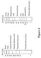
- Figure 4 illustrates one embodiment of a request packet from one of the memory ports Port 1 - Port N to the system controller 16.
- the request packet is transferred in two cycles via the appropriate memory path to the system controller 16.
- the physical address of the request packet specifies a datablock of the main memory 14 for the request packet.
- the transaction type field of the first cycle of the request packet indicates the write invalidate transaction type.
- the IVA bit indicates whether the processor subsystem 20 requires an invalidate request for the corresponding write invalidate transaction to invalidate the datablock in the external cache 74 and tags 76.
- Figure 5 illustrates a block store operation by the processor subsystem 20 for one embodiment.
- the block store operation may occur, for example, during a block copy by the processor subsystem 20.
- the processor 70 issues a block store operation to the external cache 74.
- the port interface 72 generates a write invalidate request packet that specifies the datablock of the block store operation from the processor 70.
- the processor 70 determines whether the specified datablock is being retained. If the specified datablock is not being retained by the processor 70 at decision block 104, then control proceeds to block 106.
- the processor 70 clears the IVA bit in the write invalidate request packet assembled in the port interface 72. Thereafter, at block 108 the port interface 72 issues the write invalidate request to the system controller 16 via the address path 42.
- the processor 70 determines whether the specified datablock is present in the external cache 74 by performing a tag look-up operation to the external tags 76. If the specified datablock is not present in the external cache 74, then control proceeds to block 108 to issue the write invalidate.request to the system controller 16. Otherwise control proceeds to block 112.
- the processor 70 sets the IVA bit in the write invalidate request packet to indicate that a write invalidate request for the datablock is required from the system controller 16. Thereafter, control proceeds to block 108 to issue the write invalidate request packet to the system controller 16.
Description
- The present invention pertains to the field of computer systems. More particularly, this invention relates to a computer system that includes a system level mechanism for invalidating data stored in the external cache of a processor in the computer system.
- Prior computer systems typically include one or more processor subsystems and one or more input/output subsystems coupled to a main memory subsystem. Such a main memory subsystem typically provides storage areas for instructions and data for the processors, as well as storage areas for data transfer to and from input/output devices coupled to the input/output subsystem. Typically, the processor subsystems and the input/output subsystems are coupled to the main memory subsystem via a physical interconnect that provides a common bus or a switched interconnect data path.
- A processor subsystem in such a system typically includes an associated external cache memory. Such an external cache memory usually stores selected blocks from the main memory subsystem. An external cache memory usually provides fast processor access to code and data by avoiding external fetches to the main memory subsystem for datablocks that are stored in the cache. In addition, such a computer system typically implements a protocol for maintaining data coherency between the main memory and the corresponding datablocks in the external cache memory. For example, each external cache memory typically includes a set of tags that indicate the validity status of the datablocks stored in the external cache.
- Typically, such a computer system provides a mechanism for performing coherent data input/output. For example, an input/output subsystem in such a computer system commonly injects new data into the system by issuing write invalidate (WRI) operations to the main memory subsystem. Such write invalidate operations may occur, for example, when a new page of data is read from a disk device coupled to the input/output subsystem.
- In addition, a processor subsystem commonly injects new data into the computer system using WRI operations during block copy operations. Such block copy operations occur, for example, during data structure initialization or during file copy operations in the computer system. Such block copy operations occur at a relatively high rate in a typical prior computer system.
- Such WRI operations usually require the invalidation of corresponding data blocks stored in an external processor caches to maintain data coherency in the system. Typically, such an invalidate operation on an external cache is only necessary when the tags for that external cache indicate that the newly injected datablock is present.
- In some prior computer systems, such an invalidation operation is performed within each processor subsystem. In such a system, a processor reads the corresponding external tags to determine whether an invalidate operation is required during a write invalidate transaction. However, such a mechanism requires that each processor perform a tag read operation and potentially a tag read-modify-write operation for each WRI operation issued to the memory subsystem. Such WRI operations occur at a frequent rate in typical prior systems and interfere with normal instruction execution by the processors, thereby slowing the overall performance of such a system. Moreover, processor subsystems that perform such self-invalidation operations may be incompatible with systems that provide directory based tags in the memory subsystem.
- Some computer systems may implement a worst case approach to such invalidate operations. For example, a system may blindly perform an external cache invalidate operation for every write invalidate transaction whether or not the datablock specified by the write invalidate transaction is present in the external cache. Such an invalidate operation is unnecessary whenever the specified datablock is not stored in the external cache. Unfortunately, such unnecessary invalidate operations interfere with normal operations of the processor.
- In addition, such invalidate operations may be required during some types block copy operations while not during other types of block copy operations. For example, a processor subsystem may require an invalidate operation during block copy operations that generate new memory datablocks that the processor subsystem will not later access. On the other hand, block copy operations that write datablocks to stable storage in the computer system typically do not require an invalidate operation to the external cache if the processor retains control over the datablocks transferred to stable storage. Prior systems that blindly perform invalidate operations usually cause the processor subsystem to later perform an external fetch to the memory subsystem for the specified datablocks. Unfortunately, such unnecessary external fetches to the memory subsystem slows the overall throughput of such a computer system.
- IEEE Micro, vol. 14, No. 5, 1 October 1994, pages 52-59, "Hardware Approaches to Cache Coherence in Shared-Memory Multiprocessors,
Part 1", reviews known protocols such as Directory protocols and alternative Snoopy protocols for maintaining data coherency between a main memory and the corresponding data blocks in an external cache memory. - According to one aspect, the invention consists in a computer system comprising a processor subsystem having an external cache memory; and a memory subsystem coupled to the processor subsystem, the memory subsystem being separate from the processor subsystem, the processor subsystem issuing a write invalidate (WRI) operation specifying a data block to be stored in memory subsystem, characterised in that the WRI operation includes an invalidate advisory (IVA) indication that indicates to the memory whether the data block is present in the external cache, the IVA indication determining whether the memory subsystem, in response to receiving the WRI operation, sends a message to said processor subsystem to invalidate the data block, and the method of operating the computer system.
- According to another aspect, the invention consists in a computer system comprising: a processor subsystem having an external cache memory and associated cache tags; and a memory interconnect including a mechanism for invalidating a data block in the external cache memory, the memory interconnect further being separate from the processor subsystem, wherein the memory interconnect invalidates the data block in response to an invalidate advisory (IVA) indication included in a write invalidate (WRI) operation issued by the processor subsystem that specifies the data block.
- According to yet another aspect, the invention consists in a method for transferring a method for transferring data to a memory interconnect, the memory interconnect being separate from but coupled to a processor subsystem, the processor subsystem including an external cache memory, the method comprising the steps of: determining whether a data block is present in the external cache memory; issuing a write invalidate (WRI) operation specifying the data block to be stored in the memory interconnect, wherein the WRI operation further includes an invalidate advisory (IVA) indication that indicates to the memory interconnect whether the data block is present in the external cache memory; and invalidating the data block in response to detecting the IVA indication.
- The mechanism in the memory subsystem or memory interconnect for invalidating the external cache of the processor simplifies the design of the processor to external cache interface and reduces the impact on processor performance of write invalidate operations in the system. Such an external mechanism for cache invalidation also eliminates read-modify-write operations by the processor to the external cache during write invalidate operations that would otherwise impact processor performance. In addition, such an external mechanism for cache invalidation provides a processor subsystem that is compatible with multiprocessor systems that maintain directory based or duplicate tags and with uniprocessor systems that do not maintain directory based or duplicate tags.
- Other features and advantages of the present invention will be apparent from the accompanying drawings, and from the detailed description that follows below.
- The present invention is illustrated by way of example and not limitation in the figures of the accompanying drawings in which like references indicate similar elements, and in which:
- Figure 1 illustrates a
computer system 10 for one embodiment including a processor subsystem, an input/output port, and a memory interconnect subsystem; - Figure 2 illustrates a processor subsystem which includes a processor, an external cache and associated set of external tags, and a memory interconnect port interface;
- Figure 3 illustrates the input/output port for one embodiment including a standard input/output bus interface and a port interface that enables coherent input/output direct memory access to the main memory;
- Figure 4 illustrates one embodiment of a request packet from one of the memory ports Port 1 - Port N to the system controller;
- Figure 5 illustrates the handling of a block store operation by the processor subsystem for one embodiment.
-
- Figure 1 illustrates a
computer system 10 for one embodiment. Thecomputer system 10 comprises aprocessor subsystem 10, and an input/output port 22, and amemory interconnect subsystem 18. Thememory interconnect subsystem 18 provides shared access to amain memory 14 to theprocessor subsystem 20 and the input/output subsystem 22. Elements of thecomputer system 10 communicate with thememory interconnect subsystem 18 via a set of memory ports 1-N. For example,port 1 for theprocessor subsystem 20 comprises adata path 40, anaddress path 42, and acontrol path 44, and port N for the input/output subsystem 22 comprises adata path 46, anaddress path 48 and acontrol path 50. - The
memory interconnect subsystem 18 includes adata path switch 12 to themain memory 14, and asystem controller 16. For one embodiment, thedata path switch 12 is a cross bar switch controlled by thesystem controller 16 via a set of control signals 54. Thedata path switch 12 enables data path access to themain memory 14 via the data path of each port 1-N including thedata path 40 and thedata path 46. Thesystem controller 16 functions as a memory controller by decoding the addresses received from the processor subsystems and I/O subsystem 20-22 and by generating memory control signals including row address select (RAS) and column address select (CAS) signals to themain memory 14 via amemory control bus 56. - The
system controller 16 receives memory access requests from the subsystems 20-22 via the address path of each port 1-N including theaddress path 42 and theaddress path 48. Thesystem controller 16 arbitrates among the requests from the subsystems 20-22 and configures thedata path switch 12 to provide the necessary connections for access to themain memory 14 via amemory data bus 52 or for subsystem to subsystem data transfers. Thesystem controller 16 responds with cache state transition control messages to theprocessor subsystem 20 when necessary. - The memory access requests include, for example, write invalidate (WRI) requests. The subsystems 20-22 use a WRI request to the
system controller 16 to write a specified datablock into themain memory 14. Thesystem controller 16 processes a WRI request by configuring the data path switch 12 to provide the proper source for the specified datablock. If the WRI request originates with theprocessor subsystem 20, then thesystem controller 16 transfers messages via thecontrol path 44 to control the cache state transitions in the external cache of theprocessor subsystem 20. For example, thesystem controller 16 transfers invalidate messages via thecontrol path 44 to invalidate datablocks in the external cache of theprocessor subsystem 20 when appropriate. - In another embodiment, the
system controller 16 maintains a set of duplicate tags that correspond to the external tags. In such a multiprocessor embodiment, thesystem controller 16 accesses the duplicate tags via a snoop bus coupled between thesystem controller 16 and the duplicate tags. For an illustration of such an embodiment, refer to application serial no. , filed on March 31, 1995, and entitled Packet Switched Cache Coherent Multiprocessor Computer System. - The input/
output port 22 enables communication with a set of peripheral devices 30-33 via a standardized input/output bus 58. The standardized input/output bus 58 may comprise, for example, a SBUS or a peripheral component interconnect (PCI) standardized bus. The input/output port 22 implements a direct memory access mechanism that provides coherent input/output operations to themain memory 14 through thesystem controller 16. - Figure 2 illustrates the
processor subsystem 20 for one embodiment. Theprocessor subsystem 20 comprises aprocessor 70, anexternal cache 74, and an associated set ofexternal tags 76 along with aport interface 72. - The
processor 70 issues memory load and memory store operations to theexternal cache 74. Theport interface 72 issues a cache requests to thesystem controller 16 using a message packet transferred via theaddress pass 42. The cache requests include WRI transactions during block copy operations by theprocessor 70. Each message packet transferred via theaddress pass 42 includes a header that specifies the write invalidate request type along with an address that specifies the datablock for the write invalidate transaction. Thesystem controller 16 processes a write invalidate transaction by configuring thedatapath switch 12 to transfer the corresponding datablock to themain memory 14. - For one embodiment, the WRI request packet to the
system controller 16 includes an invalidate advisory (IVA) indication. The IVA indication determines whether thesystem controller 16 issues an invalidate request back to theprocessor subsystem 20 to invalidate the corresponding datablock in theexternal cache 74. In addition, theprocessor subsystem 20 performs a copyback operation to thememory interconnect subsystem 18 in response to the invalidate request if the specified invalidated datablock is present in theexternal cache 74. - Figure 3 illustrates the input/
output port 22 for one embodiment. The input/output port 22 comprises a standard input/output bus interface 80 along with aport interface 82. Theport interface 82 enables coherent input/output direct memory access to themain memory 14 through thesystem controller 16. - Figure 4 illustrates one embodiment of a request packet from one of the memory ports Port 1 - Port N to the
system controller 16. For this embodiment, the request packet is transferred in two cycles via the appropriate memory path to thesystem controller 16. The physical address of the request packet specifies a datablock of themain memory 14 for the request packet. During a WRI transaction from theprocessor subsystem 20, the transaction type field of the first cycle of the request packet indicates the write invalidate transaction type. The IVA bit indicates whether theprocessor subsystem 20 requires an invalidate request for the corresponding write invalidate transaction to invalidate the datablock in theexternal cache 74 and tags 76. - Figure 5 illustrates a block store operation by the
processor subsystem 20 for one embodiment. The block store operation may occur, for example, during a block copy by theprocessor subsystem 20. Atblock 100, theprocessor 70 issues a block store operation to theexternal cache 74. - At
block 102 theport interface 72 generates a write invalidate request packet that specifies the datablock of the block store operation from theprocessor 70. Atdecision block 104, theprocessor 70 determines whether the specified datablock is being retained. If the specified datablock is not being retained by theprocessor 70 atdecision block 104, then control proceeds to block 106. - At
block 106, theprocessor 70 clears the IVA bit in the write invalidate request packet assembled in theport interface 72. Thereafter, atblock 108 theport interface 72 issues the write invalidate request to thesystem controller 16 via theaddress path 42. - If the specified datablock is being retained by the
processor 70 atdecision block 104, then control proceeds todecision block 110. Atdecision block 110, theprocessor 70 determines whether the specified datablock is present in theexternal cache 74 by performing a tag look-up operation to the external tags 76. If the specified datablock is not present in theexternal cache 74, then control proceeds to block 108 to issue the write invalidate.request to thesystem controller 16. Otherwise control proceeds to block 112. - At
block 112 theprocessor 70 sets the IVA bit in the write invalidate request packet to indicate that a write invalidate request for the datablock is required from thesystem controller 16. Thereafter, control proceeds to block 108 to issue the write invalidate request packet to thesystem controller 16.
Claims (10)
- A computer system comprising:a processor subsystem (20) having an external cache memory (74); anda memory subsystem (18) coupled to the processor subsystem, the memory subsystem being separate from the processor subsystem, the processor subsystem issuing a write invalidate (WRI) operation specifying a data block to be stored in memory subsystem, characterised in that the WRI operation includes an invalidate advisory (IVA) indication that indicates to the memory whether the data block is present in the external cache, the IVA indication determining whether the memory subsystem, in response to receiving the WRI operation, sends a message to said processor subsystem to invalidate the data block.
- The computer system of claim 1 further comprising:I/O subsystem coupled to the memory subsystem, the data block originating from the I/O subsystem.
- The computer system of claim 1 wherein the IVA indication is a single bit, the bit being set to indicate the data block is present in the external cache (74), the memory subsystem sending the message to invalidate the data block in response to detecting the bit as set.
- The computer system of claim 1 further comprising: a plurality of cache tags (76) associated with the external cache memory (74), the processor subsystem (20) performing a cache tag look-up operation to determine whether the data block is present in the external cache.
- The computer system of claim 1 wherein the processor subsystem (20) includes cache tags (76) associated with the external cache memory (74).
- The computer system of claim 5 further comprising:a plurality of duplicate tags maintained by the memory subsystem (18), the duplicate tags corresponding to the cache tags (76) in the processor subsystem (20).
- The computer system of claim 1 wherein the memory subsystem (18) includes a mechanism for invalidating a data block in the external cache memory (74)
- A method for transferring data to a memory interconnect (18), the memory interconnect being separate from but coupled to a processor subsystem (20), the processor subsystem including an external cache memory (74), the method comprising the steps of:determining whether a data block is present in the external cache memory;issuing a write invalidate (WRI) operation specifying the data block to be stored in the memory interconnect (18), characterised in that the WRI operation further includes an invalidate advisory (IVA) indication that indicates to the memory interconnect whether the data block is present in the external cache memory (74); andinvalidating the data block in the processor subsystem in response to a message originating from the memory sent in response to the receipt of an invalidate advisory indication.
- The method of claim 8 wherein the step of issuing a WRI operation includes specifying a data block that originates from I/O subsystem coupled to the memory interconnect (18).
- The method of claim 8 wherein the step of determining whether a data block is present in the external cache memory (74) includes the step of performing a cache look-up operation.
Applications Claiming Priority (2)
| Application Number | Priority Date | Filing Date | Title |
|---|---|---|---|
| US41436595A | 1995-03-31 | 1995-03-31 | |
| US414365 | 1995-03-31 |
Publications (2)
| Publication Number | Publication Date |
|---|---|
| EP0735481A1 EP0735481A1 (en) | 1996-10-02 |
| EP0735481B1 true EP0735481B1 (en) | 2003-05-14 |
Family
ID=23641138
Family Applications (1)
| Application Number | Title | Priority Date | Filing Date |
|---|---|---|---|
| EP96301804A Expired - Lifetime EP0735481B1 (en) | 1995-03-31 | 1996-03-15 | System level mechanism for invalidating data stored in the external cache of a processor in a computer system |
Country Status (5)
| Country | Link |
|---|---|
| US (1) | US5737755A (en) |
| EP (1) | EP0735481B1 (en) |
| JP (1) | JP3887036B2 (en) |
| DE (1) | DE69628079T2 (en) |
| SG (1) | SG50950A1 (en) |
Families Citing this family (2)
| Publication number | Priority date | Publication date | Assignee | Title |
|---|---|---|---|---|
| US5835950A (en) * | 1996-07-12 | 1998-11-10 | Samsung Electronics Co., Ltd. | Self-invalidation method for reducing coherence overheads in a bus-based shared-memory multiprocessor apparatus |
| US6412047B2 (en) * | 1999-10-01 | 2002-06-25 | Stmicroelectronics, Inc. | Coherency protocol |
Family Cites Families (32)
| Publication number | Priority date | Publication date | Assignee | Title |
|---|---|---|---|---|
| US4228503A (en) * | 1978-10-02 | 1980-10-14 | Sperry Corporation | Multiplexed directory for dedicated cache memory system |
| US4638431A (en) * | 1984-09-17 | 1987-01-20 | Nec Corporation | Data processing system for vector processing having a cache invalidation control unit |
| DE3740834A1 (en) * | 1987-01-22 | 1988-08-04 | Nat Semiconductor Corp | MAINTAINING COHERENCE BETWEEN A MICROPROCESSOR-INTEGRATED CACHE AND AN EXTERNAL MEMORY |
| JPH065524B2 (en) * | 1987-11-18 | 1994-01-19 | インターナショナル・ビジネス・マシーンズ・コーポレーション | Storage device management method |
| US5058006A (en) * | 1988-06-27 | 1991-10-15 | Digital Equipment Corporation | Method and apparatus for filtering invalidate requests |
| US5226146A (en) * | 1988-10-28 | 1993-07-06 | Hewlett-Packard Company | Duplicate tag store purge queue |
| EP0380842A3 (en) * | 1989-02-03 | 1991-06-12 | Digital Equipment Corporation | Method and apparatus for interfacing a system control unit for a multiprocessor system with the central processing units |
| US5222224A (en) * | 1989-02-03 | 1993-06-22 | Digital Equipment Corporation | Scheme for insuring data consistency between a plurality of cache memories and the main memory in a multi-processor system |
| CA1325289C (en) * | 1989-02-03 | 1993-12-14 | Digital Equipment Corporation | Scheme for insuring data consistency between a plurality of cache memories and the main memory in a multi-processor computer system |
| US5036459A (en) * | 1989-03-09 | 1991-07-30 | U.S. Philips Corporation | Multi-processor computer system with distributed memory and an interprocessor communication mechanism, and method for operating such mechanism |
| JPH0666056B2 (en) * | 1989-10-12 | 1994-08-24 | 甲府日本電気株式会社 | Information processing system |
| JP2833062B2 (en) * | 1989-10-30 | 1998-12-09 | 株式会社日立製作所 | Cache memory control method, processor and information processing apparatus using the cache memory control method |
| US5297269A (en) * | 1990-04-26 | 1994-03-22 | Digital Equipment Company | Cache coherency protocol for multi processor computer system |
| US5249284A (en) * | 1990-06-04 | 1993-09-28 | Ncr Corporation | Method and system for maintaining data coherency between main and cache memories |
| EP0468831B1 (en) * | 1990-06-29 | 1997-10-15 | Digital Equipment Corporation | Bus protocol for write-back cache processor |
| US5193170A (en) * | 1990-10-26 | 1993-03-09 | International Business Machines Corporation | Methods and apparatus for maintaining cache integrity whenever a cpu write to rom operation is performed with rom mapped to ram |
| CA2051209C (en) * | 1990-11-30 | 1996-05-07 | Pradeep S. Sindhu | Consistency protocols for shared memory multiprocessors |
| US5265235A (en) * | 1990-11-30 | 1993-11-23 | Xerox Corporation | Consistency protocols for shared memory multiprocessors |
| JPH04318654A (en) * | 1991-02-13 | 1992-11-10 | Hewlett Packard Co <Hp> | Redirection system for interruption to microprocessor |
| US5303362A (en) * | 1991-03-20 | 1994-04-12 | Digital Equipment Corporation | Coupled memory multiprocessor computer system including cache coherency management protocols |
| JP2703417B2 (en) * | 1991-04-05 | 1998-01-26 | 富士通株式会社 | Receive buffer |
| AU2270892A (en) * | 1991-06-26 | 1993-01-25 | Ast Research, Inc. | Automatic distribution of interrupts controller for a multiple processor computer system |
| JPH0512117A (en) * | 1991-07-04 | 1993-01-22 | Toshiba Corp | Cache matching system |
| DE69230428T2 (en) * | 1991-09-27 | 2000-08-03 | Sun Microsystems Inc | Bus arbitration architecture containing deadlock detection and masking |
| EP0553743A1 (en) * | 1992-01-31 | 1993-08-04 | Motorola, Inc. | A cache controller |
| US5553266A (en) * | 1992-04-24 | 1996-09-03 | Digital Equipment Corporation | Update vs. invalidate policy for a snoopy bus protocol |
| US5319766A (en) * | 1992-04-24 | 1994-06-07 | Digital Equipment Corporation | Duplicate tag store for a processor having primary and backup cache memories in a multiprocessor computer system |
| US5319753A (en) * | 1992-09-29 | 1994-06-07 | Zilog, Inc. | Queued interrupt mechanism with supplementary command/status/message information |
| US5434993A (en) * | 1992-11-09 | 1995-07-18 | Sun Microsystems, Inc. | Methods and apparatus for creating a pending write-back controller for a cache controller on a packet switched memory bus employing dual directories |
| US5604882A (en) * | 1993-08-27 | 1997-02-18 | International Business Machines Corporation | System and method for empty notification from peer cache units to global storage control unit in a multiprocessor data processing system |
| JPH07105031A (en) * | 1993-09-20 | 1995-04-21 | Internatl Business Mach Corp <Ibm> | Method and apparatus for transfer of interrupt information at inside of multiprocessor computer system |
| US5603005A (en) * | 1994-12-27 | 1997-02-11 | Unisys Corporation | Cache coherency scheme for XBAR storage structure with delayed invalidates until associated write request is executed |
-
1996
- 1996-03-15 DE DE69628079T patent/DE69628079T2/en not_active Expired - Fee Related
- 1996-03-15 EP EP96301804A patent/EP0735481B1/en not_active Expired - Lifetime
- 1996-03-29 SG SG1996006437A patent/SG50950A1/en unknown
- 1996-03-29 JP JP09959596A patent/JP3887036B2/en not_active Expired - Lifetime
-
1997
- 1997-02-12 US US08/797,995 patent/US5737755A/en not_active Expired - Lifetime
Also Published As
| Publication number | Publication date |
|---|---|
| DE69628079T2 (en) | 2004-02-26 |
| EP0735481A1 (en) | 1996-10-02 |
| JP3887036B2 (en) | 2007-02-28 |
| SG50950A1 (en) | 1998-07-20 |
| JPH0922382A (en) | 1997-01-21 |
| US5737755A (en) | 1998-04-07 |
| DE69628079D1 (en) | 2003-06-18 |
Similar Documents
| Publication | Publication Date | Title |
|---|---|---|
| US5706463A (en) | Cache coherent computer system that minimizes invalidation and copyback operations | |
| US7228389B2 (en) | System and method for maintaining cache coherency in a shared memory system | |
| US6401174B1 (en) | Multiprocessing computer system employing a cluster communication error reporting mechanism | |
| US5426765A (en) | Multiprocessor cache abitration | |
| US6760819B2 (en) | Symmetric multiprocessor coherence mechanism | |
| US6651115B2 (en) | DMA controller and coherency-tracking unit for efficient data transfers between coherent and non-coherent memory spaces | |
| US7032074B2 (en) | Method and mechanism to use a cache to translate from a virtual bus to a physical bus | |
| US5943684A (en) | Method and system of providing a cache-coherency protocol for maintaining cache coherency within a multiprocessor data-processing system | |
| US5561779A (en) | Processor board having a second level writeback cache system and a third level writethrough cache system which stores exclusive state information for use in a multiprocessor computer system | |
| KR920004402B1 (en) | Bus interface circuit for digital data processor | |
| US6279085B1 (en) | Method and system for avoiding livelocks due to colliding writebacks within a non-uniform memory access system | |
| US5806086A (en) | Multiprocessor memory controlling system associating a write history bit (WHB) with one or more memory locations in controlling and reducing invalidation cycles over the system bus | |
| JPH0247756A (en) | Reading common cash circuit for multiple processor system | |
| KR20010101193A (en) | Non-uniform memory access(numa) data processing system that speculatively forwards a read request to a remote processing node | |
| US4831581A (en) | Central processor unit for digital data processing system including cache management mechanism | |
| KR19980079662A (en) | Shared Intervention Method of Cache Lines in SMP Bus Shared State | |
| KR19980079663A (en) | Shared Intervention Method of Cache Lines in Recent Read State of SMP Bus | |
| US6269428B1 (en) | Method and system for avoiding livelocks due to colliding invalidating transactions within a non-uniform memory access system | |
| JP2000250884A (en) | Method and system for providing eviction protocol in unequal memory access computer system | |
| US5829027A (en) | Removable processor board having first, second and third level cache system for use in a multiprocessor computer system | |
| JP2000250883A (en) | Method and system for avoiding loss of data caused by cancel of transaction in unequal memory access system | |
| US5611074A (en) | Efficient polling technique using cache coherent protocol | |
| US10949292B1 (en) | Memory interface having data signal path and tag signal path | |
| US20040111563A1 (en) | Method and apparatus for cache coherency between heterogeneous agents and limiting data transfers among symmetric processors | |
| US20020019913A1 (en) | Coherency protocol |
Legal Events
| Date | Code | Title | Description |
|---|---|---|---|
| PUAI | Public reference made under article 153(3) epc to a published international application that has entered the european phase |
Free format text: ORIGINAL CODE: 0009012 |
|
| AK | Designated contracting states |
Kind code of ref document: A1 Designated state(s): DE FR GB IT NL SE |
|
| 17P | Request for examination filed |
Effective date: 19970327 |
|
| 17Q | First examination report despatched |
Effective date: 20010109 |
|
| GRAG | Despatch of communication of intention to grant |
Free format text: ORIGINAL CODE: EPIDOS AGRA |
|
| GRAG | Despatch of communication of intention to grant |
Free format text: ORIGINAL CODE: EPIDOS AGRA |
|
| GRAH | Despatch of communication of intention to grant a patent |
Free format text: ORIGINAL CODE: EPIDOS IGRA |
|
| GRAH | Despatch of communication of intention to grant a patent |
Free format text: ORIGINAL CODE: EPIDOS IGRA |
|
| GRAA | (expected) grant |
Free format text: ORIGINAL CODE: 0009210 |
|
| AK | Designated contracting states |
Designated state(s): DE FR GB IT NL SE |
|
| REG | Reference to a national code |
Ref country code: GB Ref legal event code: FG4D |
|
| RAP2 | Party data changed (patent owner data changed or rights of a patent transferred) |
Owner name: SUN MICROSYSTEMS, INC. |
|
| REF | Corresponds to: |
Ref document number: 69628079 Country of ref document: DE Date of ref document: 20030618 Kind code of ref document: P |
|
| NLT2 | Nl: modifications (of names), taken from the european patent patent bulletin |
Owner name: SUN MICROSYSTEMS, INC. |
|
| REG | Reference to a national code |
Ref country code: SE Ref legal event code: TRGR |
|
| PGFP | Annual fee paid to national office [announced via postgrant information from national office to epo] |
Ref country code: FR Payment date: 20040309 Year of fee payment: 9 |
|
| PG25 | Lapsed in a contracting state [announced via postgrant information from national office to epo] |
Ref country code: SE Free format text: LAPSE BECAUSE OF NON-PAYMENT OF DUE FEES Effective date: 20040316 |
|
| PLBE | No opposition filed within time limit |
Free format text: ORIGINAL CODE: 0009261 |
|
| STAA | Information on the status of an ep patent application or granted ep patent |
Free format text: STATUS: NO OPPOSITION FILED WITHIN TIME LIMIT |
|
| ET | Fr: translation filed | ||
| 26N | No opposition filed |
Effective date: 20040217 |
|
| PG25 | Lapsed in a contracting state [announced via postgrant information from national office to epo] |
Ref country code: NL Free format text: LAPSE BECAUSE OF NON-PAYMENT OF DUE FEES Effective date: 20041001 |
|
| EUG | Se: european patent has lapsed | ||
| NLV4 | Nl: lapsed or anulled due to non-payment of the annual fee |
Effective date: 20041001 |
|
| PG25 | Lapsed in a contracting state [announced via postgrant information from national office to epo] |
Ref country code: IT Free format text: LAPSE BECAUSE OF NON-PAYMENT OF DUE FEES Effective date: 20050315 |
|
| PG25 | Lapsed in a contracting state [announced via postgrant information from national office to epo] |
Ref country code: FR Free format text: LAPSE BECAUSE OF NON-PAYMENT OF DUE FEES Effective date: 20051130 |
|
| REG | Reference to a national code |
Ref country code: FR Ref legal event code: ST Effective date: 20051130 |
|
| PGFP | Annual fee paid to national office [announced via postgrant information from national office to epo] |
Ref country code: DE Payment date: 20070308 Year of fee payment: 12 |
|
| PG25 | Lapsed in a contracting state [announced via postgrant information from national office to epo] |
Ref country code: DE Free format text: LAPSE BECAUSE OF NON-PAYMENT OF DUE FEES Effective date: 20081001 |
|
| PGFP | Annual fee paid to national office [announced via postgrant information from national office to epo] |
Ref country code: GB Payment date: 20150311 Year of fee payment: 20 |
|
| REG | Reference to a national code |
Ref country code: GB Ref legal event code: PE20 Expiry date: 20160314 |
|
| PG25 | Lapsed in a contracting state [announced via postgrant information from national office to epo] |
Ref country code: GB Free format text: LAPSE BECAUSE OF EXPIRATION OF PROTECTION Effective date: 20160314 |