EP0738910B1 - Improvements relating to a digital micromirror device - Google Patents
Improvements relating to a digital micromirror device Download PDFInfo
- Publication number
- EP0738910B1 EP0738910B1 EP96106099A EP96106099A EP0738910B1 EP 0738910 B1 EP0738910 B1 EP 0738910B1 EP 96106099 A EP96106099 A EP 96106099A EP 96106099 A EP96106099 A EP 96106099A EP 0738910 B1 EP0738910 B1 EP 0738910B1
- Authority
- EP
- European Patent Office
- Prior art keywords
- yoke
- spatial light
- light modulator
- specified
- mirror
- Prior art date
- Legal status (The legal status is an assumption and is not a legal conclusion. Google has not performed a legal analysis and makes no representation as to the accuracy of the status listed.)
- Expired - Lifetime
Links
Images


Classifications
-
- G—PHYSICS
- G02—OPTICS
- G02B—OPTICAL ELEMENTS, SYSTEMS OR APPARATUS
- G02B26/00—Optical devices or arrangements for the control of light using movable or deformable optical elements
-
- G—PHYSICS
- G02—OPTICS
- G02B—OPTICAL ELEMENTS, SYSTEMS OR APPARATUS
- G02B26/00—Optical devices or arrangements for the control of light using movable or deformable optical elements
- G02B26/08—Optical devices or arrangements for the control of light using movable or deformable optical elements for controlling the direction of light
- G02B26/0816—Optical devices or arrangements for the control of light using movable or deformable optical elements for controlling the direction of light by means of one or more reflecting elements
- G02B26/0833—Optical devices or arrangements for the control of light using movable or deformable optical elements for controlling the direction of light by means of one or more reflecting elements the reflecting element being a micromechanical device, e.g. a MEMS mirror, DMD
- G02B26/0841—Optical devices or arrangements for the control of light using movable or deformable optical elements for controlling the direction of light by means of one or more reflecting elements the reflecting element being a micromechanical device, e.g. a MEMS mirror, DMD the reflecting element being moved or deformed by electrostatic means
Definitions
- the present invention is generally related to spatial light modulators for modulating incident light to form an optical light image, and more particularly, to a digital micromirror device (DMD) having an array of bistable micromirrors fabricated over addressing circuitry.
- DMD digital micromirror device
- SLMs Spatial Light Modulators
- SLMs have found numerous applications in the areas of optical information processing, projection displays, video and graphics monitors, televisions, and electrophotographic printing.
- SLMs are devices that modulate incident light in a spatial pattern to form a light image corresponding to an electrical or optical input.
- the incident light may be modulated in its phase, intensity, polarization, or direction.
- the light modulation may be achieved by a variety of materials exhibiting various electro-optic or magneto-optic effects, and by materials that modulate light by surface deformation.
- An SLM is typically comprised of an area or linear array of addressable picture elements (pixels).
- Source pixel data is first formatted by an associated control circuit, usually external to the SLM, and then loaded into the pixel array one frame at a time.
- This pixel data may be written to the pixel array using a variety of algorithms, i.e. sequentially top-to-bottom one pixel line at a time, interleaving by sequentially addressing top-to-bottom ever other pixel line, such as the odd rows of pixels, and then returning to address the even pixel lines, etc.
- this data writing technique is know as rasterizing, whereby a high powered electron gun scans across the pixel elements of a phosphor screen left to right, one line at a time.
- This pixel address data writing scheme is equally applicable to liquid crystal displays (LCDs) as well.
- the DMD is an electro/mechanical/optical SLM suitable for use in displays, projectors and hard copy printers.
- the DMD is a monolithic single-chip integrated circuit SLM, comprised of a high density array of 16 ⁇ m square movable micromirrors on 17 ⁇ m centers. These mirrors are fabricated over address circuitry including an array of SRAM cells and address electrodes. Each mirror forms one pixel of the DMD array and is bistable, that is to say, stable in one of two positions, wherein a source of light directed upon the mirror array will be reflected in one of two directions.
- each mirror of the array is individually controlled to either direct incident light into the projector lens, or to the light absorber.
- the projector lens ultimately focuses and magnifies the modulated light from the pixel mirrors onto a display screen and produce an image in the case of a display. If each pixel mirror of the DMD array is in the "on" position, the displayed image will be an array of bright pixels.
- the DMD is revolutionary in that it is truly a digital display device and an integrated circuit solution.
- the evolution and variations of the DMD can be appreciated through a reading of several commonly assigned patents.
- the "first generation" of DMD spatial light modulators implemented a deflectable beam wherein the mirror and the beam were one in the same. That is, an electrostatic force was created between the mirror and the underlying address electrode to induce deflection thereof.
- the deflection of these mirrors can be variable and operate in the analog mode, and may comprise a leaf-spring or cantilevered beam, as disclosed in commonly assigned U.S. Patent 4,662,746 to Hornbeck, entitled “Spatial Light Modulator and Method", U.S.
- Patent 4,710,732 to Hornbeck entitled “Spatial Light Modulator and Method”
- U.S. Patent 4,956,619 to Hornbeck entitled “Spatial Light Modulator”
- U.S. Patent 5,172,262 to Hornbeck entitled “Spatial Light Modulator and Method”.
- This first generation DMD can also be embodied as a digital or bistable device.
- the beam (mirror) can include a mirror supported by a torsion hinge and axially rotated one of two directions 10 degrees, until the mirror tip lands upon a landing pad.
- the landing pads may be passivated by an oriented monolayer formed upon the landing pad. This monolayer decreases the Van der Waals forces and prevents sticking of the mirror to the electrode.
- This technique is disclosed in commonly assigned U.S. Patent 5,331,454 to Hornbeck, entitled “Low Reset Voltage Process for DMD”.
- a “second generation” of the DMD is embodied in commonly assigned U.S. Patent 5,083,857 entitled “Multi-Level Deformable Mirror Device”, as well as in co-pending European patent application serial number 94120234.3 entitled “Improved Multi-Level digital Micromirror Device”, filed December 20, 1994, publication number 0664470, published July 26, 1995.
- the mirror is elevated above a yoke, this yoke being suspended over the addressing circuitry by a pair of torsion hinges.
- an electrostatic force is generated between the elevated mirror and an elevated electrode. When rotated, it is the yoke that comes into contact with a landing electrode, whereby the mirror tips never come into contact with any structure.
- the shorter moment arm of the yoke being about 50% of the mirror, allows energy to be more efficiently coupled into the mirror by reset pulses due to the fact that the mirror tip is free to move.
- Applying resonant reset pulses to the mirror to help free the pivoting structure from the landing electrode is disclosed in commonly assigned U.S. Patent 5,096,279, entitled “Spatial Light Modulator and Method, and U.S. Patent 5,233,456 entitled “Resonant Mirror and Method of Manufacture".
- U.S. Patent 5,096,279 entitled “Spatial Light Modulator and Method
- U.S. Patent 5,233,456 entitled “Resonant Mirror and Method of Manufacture”.
- some of the address torque generated between the mirror and the elevated address electrode is sacrificed compared to the first generation devices because the yoke slightly diminishes the surface area of the address electrode.
- the improved DMD would preferably be fabricated using the baseline fabrication processes.
- the present invention achieves technical advantages as a DMD spatial light modulator by laterally extending the yoke in a direction parallel to the hinges, so that the yoke overlaps a substantial portion of a first pair of address electrodes.
- a second pair of elevated address electrodes are provided lateral of the yoke and beneath an elevated mirror supported by the yoke.
- Address torque is achieved between the first pair of address electrodes and the yoke, and between the elevated second pair of address electrodes and the elevated mirror.
- the yoke is spaced closer to the underlying address electrodes than the mirror is positioned relative to the elevated address electrodes.
- the present invention has superior address torque, latching torque, address holding torque and reset force compared to earlier generations, with no change in process flow.
- the present invention comprises a spatial light modulator including a substrate.
- Addressing circuitry comprising a first portion is provided proximate the substrate, and also comprises a second portion elevated above the substrate.
- a yoke is supported over the first portion of the addressing circuitry.
- At least one hinge is connected to the yoke and supports the yoke, with the hinge permitting deflection of the yoke over the addressing circuitry first portion.
- a pixel is elevated above and supported by the yoke, this pixel being positioned over the elevated addressing circuitry second portion.
- the first and second portions of the addressing circuitry are electrically connected to one another, whereby a potential provided to the first and second portions creates an electrostatic force in two places. First, an electrostatic force is generated between the yoke and the addressing circuitry first portion, and secondly, between the elevated pixel and the elevated second portion.
- the distance between the yoke and the first portion is approximately half the distance defined between the pixel and the elevated second portion.
- the opposing surface areas of the yoke and address circuitry first portion realize an addressing torque that is approximately 4 times greater than the addressing torque generated between the elevated pixel and the elevated second electrode.
- the net address torque is additive, and is substantially greater than the address torque generated by earlier generation DMD devices.
- the yoke preferably has a butterfly like shape, having a pair of yoke tips on each side of a yoke axis. When rotated, one pair of yoke tips lands upon a landing pad, whereby the supported and elevated pixel mirror remains free of any structure.
- reset pulses can be provided to the mirror, preferably at a frequency being the resonant frequency of the mirror to achieve a good reset action.
- the yoke is preferably in substantially the same plane as the hinges and may be fabricated using a single etch process so that the hinges are formed for precision alignment and balancing.
- the spatial light modulator further comprises control circuitry connected to the addressing circuitry.
- This control circuitry provides address data to both the first and second portions of the addressing circuitry to cause deflection of the pixel.
- a first portion of the addressing circuitry comprising a pad, is provided each side of the pixel axis of rotation, with a separate second portion of the addressing circuitry being provided under the pixel each side of this yoke axis.
- the control circuitry provides address data to one of either of these sets of addressing portions to cause deflection of the yoke and mirror toward the addressed first and second portions.
- the pixel is a mirror, having a rectangular shape with geometrically oriented edges at 45° with respect to the hinge to minimize diffraction terms generated along the edges of the pixel that are perceived by darkfield optics.
- the DMD device having a yoke suspended over a pair of address electrodes, and supporting an elevated mirror extending over a second pair of address electrodes, achieves a significant increase in the attractive area between address electrodes and the pivotable structure, namely, the yoke and the mirror.
- the underlying address electrodes on the substrate, comprised of metal 3, are carefully designed to maximize the attractive area while permitting the yoke tips to land on landing electrodes having the same potential as the mirror and yoke.
- the elevated address electrodes for the mirror have been modified from the second generation device to accommodate the extended yoke of the present invention, while maintaining most of the torque that can be generated between the mirror and elevated electrodes.
- Any lost torque due to a reduced area of the elevated electrodes is more than compensated for by the yoke extensions overlying the address electrodes, these address electrodes being positioned half the distance from the yoke than the mirror is positioned to the elevated electrodes.
- the net address torque that can be generated compared to the second generation device is almost a factor of two greater.
- the present invention also achieves a greater latching torque and address holding torque.
- DMD 10 is a single-chip integrated circuit seen to include an 864 X 576 micromirror array 12.
- Array 12 is monolithically fabricated over a 864 X 36 memory cell array 16.
- Each memory cell in the 36 memory cells rows (MR0-MR35) forming memory cell array 16 is associated with and controlling a dedicated group of sixteen (16) pixels 18, shown in Figure 2.
- Each memory cell comprises a primary 1-bit static random access memory (SRAM) cell, and a secondary 1-bit SRAM cell fed by the primary cell.
- SRAM static random access memory
- BL0BL863 There are 864 bit lines BL0-BL863 connected to one of each of the 864 columns of memory cells.
- Column pixel data is loaded into the addressed primary memory cell row MR n via the associated bit lines BL0-BL863.
- the primary memory cell is addressed by enabling the associated row write or read enable line, identified as the WD n or RD n , respectively, whereby WP n is connected to the enable input of each primary cell in the row MR n .
- This pixel data is latched from the primary cell into the respective secondary cell by enabling the global control line MXFRB, the MXFRB line being connected to the enable input of all secondary cells of array 16.
- the secondary memory cell essentially operates as a shadow latch, whereby data can be loaded from the primary memory cell into the secondary memory cell, allowing the primary memory cell to then be subsequently reloaded with new pixel data without effecting the memory cell contents of the secondary memory cell.
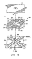
- Pixel 18 is seen to include a square mirror 30 supported upon and elevated above a yoke generally shown at 32 by a support post 34.
- Support post 34 extends downward from the center of the mirror, and is attached to the center of the yoke 32 along a torsion axis thereof, as shown, to balance the center of mass of mirror 30 upon yoke 32.
- Yoke 32 has a generally butterfly shape, that will be discussed in more detail shortly, and is axially supported along a central axis thereof by a pair of torsion hinges 40.
- the other end of each torsion hinge 40 is attached to and supported by a hinge support post cap 42 defined on top of a respective hinge support post 44.
- a pair of elevated mirror address electrodes 50 and 52 are supported by a respective address support post 54 and 56.
- the address support posts 54 and 56, and the hinge support posts 44 support the address electrodes 50 and 52, the torsion hinges 40, and the yoke 32 away from and above a bias/reset bus 60, and the pair of substrate level address electrode pads 26 and 28.
- mirror 30 and yoke 32 are together rotated about the torsion axis of the yoke 32, defined by the hinges 40, a pair of yoke tips 58 on the side of the yoke 32 that is deflected land upon and engage the bias/reset bus 60 at the landing sites 62.
- Rotation of mirror 30 and yoke 32 can be achieved in one of two directions, to achieve a bistable state and modulate incident light as shown in Figure 5 and will discussed shortly.
- An address voltage is provided to one of the two address electrodes pads 26 or 28, and to one of the corresponding elevated mirror address electrode 50 or 52 via the associated electrode support post 54 and 56. This address voltage may be 5 volts which is compatible with CMOS logic circuitry, but could also comprise of other levels if desired.
- bias/reset bus 60 bias/reset bus 60
- bias/reset bus 60 bias/reset bus 60
- yoke 32 via support post 44, post caps 42 and hinges 40, as well as to mirror 30 via support 34.
- the present invention achieves technical advantages by providing an electrostatic force between opposing surfaces at two locations illustrated by the hatched areas in Figure 2. These electrostatic attractive forces are also illustrated at 70, 76, 80 and 82 in Figure 3.
- electrostatic attraction force While an electrostatic attraction force is being generated at 70 between one half of yoke 32 and the underlying address electrode 26, an electrostatic attractive force is also being generated between the elevated address electrode 50 and mirror 30 as shown at 80 in Figure 3.
- This electrostatic attractive force is generated by the voltage potential created between the portion of mirror 30, shown at 82, defined above the elevated address electrode 50.
- the portion of mirror 30 overhanging address electrode 52 is shown at 84. Therefore, by addressing one address electrode 26 or 28, which in turn provides an address voltage to the corresponding elevated address electrode 50 or 52, electrostatic attraction force is generated at two places, shown at 70 and 80, or at 76 or 82.
- the elevated address electrodes 50 and 52 are generally co-planar with the yoke 32, each being spaced above the address electrodes 26 and 28 a distance of about 1 micron.
- the separation of mirror 30 above the elevated address electrodes 50 and 52 is approximately double this distance, or about 2 microns. Since the attractive force between opposing surfaces varies directly as a function of one over the square of the distance between the opposing surfaces, the electrostatic attractive force generated between yoke 32 and the address electrodes 26 and 28 per unit area is four times as great as the attractive force generated between mirror 30 and the corresponding elevated address electrode 50 and 52.
- the forces generated each side of the torsion axis are additive, and together cause mirror 30 and yoke 32 to be rotated in the direction toward the address electrodes.
- elevated electrodes 50 and 52 and their corresponding support posts can be eliminated.
- the height of mirror 30 above yoke 32 is only about 1 micron to achieve a strong attractive force with the underlying distal lobe of electrodes 26 and 28. When deflected, the mirror 30 will rotate toward, but will still not engage, the corresponding distal lobe of the address electrodes 26 and 28.
- the elevated structure including the posts 44, yoke 32 and mirror 30 are all of equal potential and the risk of a short is avoided. Thus, limitation to one set of elevated electrodes is not to be inferred.
- the address torque (T a ) is the torque produced by the address voltage alone with the yoke 32 and the mirror 30. This address torque is significantly greater than the address torque generated by previous generation DMD devices for like address voltages and bias potentials.
- the present invention thus has an improved address margin, which is defined as the difference between the address voltage V a and the potential that is required to ensure the mirror is rotated the proper direction when the bias voltage is applied.
- the pixel of the present invention also has an increased latching torque (T l ), which is defined as a measure of the latching torque produced by the bias voltage in the presence of an address voltage tending to rotate (or upset) the mirror to the opposite state.
- T l latching torque
- T h address-holding torque
- F r reset force
- All four of these performance parameters are substantially improved by the present invention over previous generation DMD devices due to the design of the yoke 32 generating an electrostatic attractive force with the underlying address electrodes, in combination with electrostatic attractive forces being generated between the elevated mirror 30 and the elevated address electrodes 50 and 52. Due to the proximity of the rotatable yoke 32 above the address electrodes 26 and 28, and a substantial opposing surface area thereof, all of the above mentioned performance parameters are significantly increased, and contribute to the increased electromechanical efficiency of the DMD device. In particular, for no change in hinge stiffness, a 1.8 times higher address torque is achieved over previous generation devices. The latching torque is improved by 2.6 times over that of previous DMD devices. The reset force generated is an 8.8 times increase over that of previous generation DMD devices. With all the improved performance parameters, the process for fabricating the present invention, as will be described shortly, is nearly identical to that for the previous generation devices, thus providing a benefit over previous generation devices.
- the implications of the DMD device of the present invention includes greater address margin, as discussed, less susceptibility to address upset, lower reset voltage requirements, and higher switching speeds which is critical in the operation of the device as a spatial light modulator.
- non- linear hinges can even be incorporated, with stiffer hinges if desired due to improve address margins and latching margins.
- the landing electrodes 60 can be passivated. By passivating the landing electrodes 60, the tendency for the yoke 32 to adhere or stick can be decreased. Stiction is an inhibiting force that requires large reset voltages to be applied to reset the mirror to a flat state, or to switch the mirror to the opposing deflectable bistable state.
- Methods of passivating the landing electrodes are disclosed in commonly assigned U.S. Patent 5,331,454 to Hornbeck, entitled “Low Reset Voltage Process for DMD", and in commonly assigned co-pending Japanese patent application Serial No.
- the bias/reset line can be pulsed with a voltage at a frequency corresponding to the resonant frequency of the mirror, which is typically about 5 MHZ, such as disclosed in commonly assigned U.S. Patent 5,096,279, entitled "Spatial Light Modulator and Method".
- FIG 4 a sectioned perspective view of a 3 X 3 array portion of array 12 is shown to illustrate the fabrication of the metal 3 layer upon the silicon substrate, this metal 3 layer defining the address electrodes 26 and 28 and the bias/reset buses 60 upon the silicon substrate. Also illustrated is the elevated mirror address electrodes, the post caps, and the hinges supporting yoke 32 above the metal 3 layer. The mirror support post can be seen to be supported by the respective yoke along the torsion axis of the pixel.
- FIG. 5 an optical schematic diagram is shown whereby incident light is seen to be modulated and deflected in one of two directions, depending on whether the mirror is in the "on" or “off” state.
- mirror 30 When mirror 30 is in the on state, incident light is reflected to optics including a projector lens, and ultimately focused upon a display screen in the case of a front or rear screen projector, or focused upon a photosensitive surface in the case of a electrophotographic printer.
- mirror 30 is in the off position, incident light is reflected to a light absorber and away from the darkfield optics.
- the 20° rotation between the bistable states of mirror 30 achieves a 40° swing of reflective incident light.
- the present invention achieves a high contrast ratio spatial light image, which is critical for use in darkfield optics systems for which the spatial light modulator of the present invention is intended.
- FIG. 6 a cross sectional view of pixel 18 taken alone line A-A in Figure 2 is shown with the support posts not being shown.
- yoke 32 and mirror 30 in the undeflected (flat) state, yoke 32 is generally coplanar with the elevated address electrodes 50 and 52, at a distance of about 1 micron above the metal 3 layer including address electrodes 26 and 28, and reset/bias bus 60.
- Mirror 30 is elevated above the pair of elevated address electrodes 50 and 52 about 2 microns, which is approximately double the distance separating the yoke 32 from the substrate 64.
- a silicon substrate 64 is processed so as to form the underlying address circuitry including the array of memory cells 16, the row address circuitry 20, and the column data loading circuitry 30. Thereafter, substrate 64 is covered with a protective oxide layer 102.
- a third layer of metalization commonly referred to as M3, is sputter deposited onto the partially processed wafer and being shown at 104. This third metalization layer is patterned and etched to define the address electrodes 26 and 28, as well as the bias/reset bus 60 shown in Figure 2 and Figure 4.
- a hinge spacer layer 106 is spin-deposited over the address circuitry and preferably comprises positive photoresist having a thickness of 1 micron. A pair of vias 110 are opened through the photoresist layer 106 to facilitate forming the hinge support post, then the layer of photoresist 106 is deep UV hardened at a high temperature to prevent flow and bubbling during subsequent processing steps.
- a thin hinge layer 112 of metalization is sputter deposited over the photoresist layer 106 and into vias 110, as shown.
- Hinge layer 112 preferably has a thickness of about 500 Angstroms, and can be comprised of aluminum, aluminum alloys, titanium tungsten, and other conductive materials well suited for the present invention.
- the hinge support posts 44 are defined in this step as shown, and are electrically connected to bias/reset bus 60. Also during this step, the pair of electrode support posts 54 and 56 are defined, although not shown, whereby the layer 112 is sputter deposited in a pair of corresponding vias formed in photoresist 106, these vias having been formed during the previous step when vias 110 were opened.
- the electrode support post and the hinge support post are very similar.
- the thickness of the photoresist spacer layer 106 determines the hinge air gap, and thus, determines the mirror rotation angle due to the angular freedom of yoke 32 until it engages the landing electrodes.
- a first mask of oxide is plasma-deposited, and patterned in the shape of the hinges 40. Then, a thick metal layer, typically about 3,000 Angstroms thick, of aluminum alloy is deposited.
- a second mask of oxide is plasma-deposited and then patterned in the shape of the yoke 32, the elevated electrodes 54 and 56, and the hinge support caps 42.
- the thin hinge layer 112 and the thicker metal layer are then etched to define the address electrodes 50 and 52, the hinge support caps 42, and the hinges 40, as shown.
- a single plasma etch is used to define these structures.
- the two oxide layers act as etch stops, and protect the metal layers beneath them. After completion of the plasma etch process, the oxide etch stops are removed from the thin metal hinges, the thicker metal support posts caps 42, the electrodes 50 and 54, and from the hinges 40, as shown in Figure 10.
- a thick mirror spacer layer 122 is spin-deposited over the hinges, electrodes and hinge support caps, and preferably comprises positive photoresist having a thickness of approximately 2 microns.
- a via 124 is opened in this photoresist spacer layer 122 to provide an opening above yoke 32, as shown, then the layer of photoresist 122 is deep UV hardened.
- a mirror metal layer comprising of an aluminum alloy and having reflective properties, is then sputter-deposited to a thickness of about 400 nm (4,000 Angstroms). This layer forms both the mirror support post 34 and the mirror 30.
- a masking oxide layer is then plasma-deposited onto the mirror layer, and patterned in the shape of the rectangular mirrors. The mirror metal layer is then plasma etched to form the mirror 30 and support post 34, as shown.
- the masking oxide layer is typically left in place while the wafer is subsequently processed and sawed to obtain dies.
- the chips are placed in a plasma etching chamber, where the masking oxide layer and both spacer layers 106 and 122 are plasma etched away, leaving the hinge air gap under the hinges 40 and yoke 32, as well as a mirror air gap '134 beneath the elevated mirror 30.
- Pixel 200 is seen to be very similar to pixel 18 as discussed in regards to Figure 1-13, wherein like numerals refer to like elements.
- pixel 200 has a yoke 202 which is slightly modified to have a single landing tip 204 each side of the torsion axis, as shown. When rotated, one tip 204 of yoke 202 will rotate until it engages and lands upon a corresponding landing electrode 208.
- the yoke 202 substantially overlaps each of a pair of address pads 210 and 212 formed from the metal 3 layer upon the substrate.
- Hinges 222 support yoke 202 from hinge posts 224. Elevated address electrodes 228 and 230 are coplanar with yoke 202.
- Pixel 300 is very similar to the embodiment shown in Figure 200, and to that pixel 18 shown in Figure 1-13, where like numerals refer to like elements.
- Pixel 300 also has a single landing tip provided each side of the torsion axis, similar to the embodiment in Figure 14.
- a yoke 302 is substantially extended parallel to the torsion axis and over the underlying address electrodes, where a pair of address electrodes 304 and 306 are provided beneath one side of yoke 302, and another pair of address electrodes 310 and 312 are provided on the other side of the bias/reset bus 320 which has an X-pattern, as shown.
- the two address electrodes 304 and 306 are electrically tied to one another, and the other pair of address electrodes 310 and 312 are electrically tied together.
- the pairs of address electrodes are electrically connected to the elevated mirror address electrodes 330 and 332 via a corresponding support post 336, as shown.
- the areas of electrostatic attraction are shown by the hatched areas of 350, 352, 354, 356, 358 and 360.
- Hinges 362 support yoke 302 from posts 364.
- the bias/reset bus 320 has an X-shape, and bifurcates the pair of address electrodes, as shown. With an X-shape, the bias/reset bus can be easily and conveniently interconnected to adjacent pixels in the metal 3 layer upon the silicon substrate.
- This may yield a desirable layout for controlling multiple rows of pixels with a common bias/reset bus, and also facilitates the split-reset technique, such as disclosed in commonly assigned European patent application Serial No. 94100308.9, entitled “Pixel Control Circuitry for Spatial Light Modulator " , filed January 11, 1994, publication no.0610665, publication date August 17, 1994.
- the landing cites of the yoke tips are provided along the bias/reset bus, shown at 340.
- a spatial light modulator of the DMD type having electrostatic forces generated at two locations to induce deflection of the pixel mirror.
- an attractive force is generated between the yoke and an underlying substrate address electrode.
- an electrostatic force is also generated between the elevated mirror and an elevated address electrode.
- These electrostatic forces are additive, and realize improved performance parameters over prior generation DMD devices. Since the yoke is separated above the substrate address electrodes by a distance equal to one-half the spacing between the mirror and the elevated address electrodes, an attractive force per unit area is 4 times greater than the force generated between the mirror and the elevated electrodes is achieved.
- the design of the present invention achieves higher address torques, higher latching torques, higher reset forces, and greater address margins.
- the pixel is less susceptible to address upset, requires a lower reset voltage, and may eliminate the need for resonant reset and multiple reset pulses. Higher switching speeds are achieved, whereby non-linear and stiffer hinges can be implemented due to the improved performance parameters described.
- the pixel array can be fabricated with little deviation from the baseline process. Thus, improved performance parameters are achievable with the spatial light modulator of the present invention over previous generations.
Description
- The present invention is generally related to spatial light modulators for modulating incident light to form an optical light image, and more particularly, to a digital micromirror device (DMD) having an array of bistable micromirrors fabricated over addressing circuitry.
- Spatial Light Modulators (SLMs) have found numerous applications in the areas of optical information processing, projection displays, video and graphics monitors, televisions, and electrophotographic printing. SLMs are devices that modulate incident light in a spatial pattern to form a light image corresponding to an electrical or optical input. The incident light may be modulated in its phase, intensity, polarization, or direction. The light modulation may be achieved by a variety of materials exhibiting various electro-optic or magneto-optic effects, and by materials that modulate light by surface deformation.
- An SLM is typically comprised of an area or linear array of addressable picture elements (pixels). Source pixel data is first formatted by an associated control circuit, usually external to the SLM, and then loaded into the pixel array one frame at a time. This pixel data may be written to the pixel array using a variety of algorithms, i.e. sequentially top-to-bottom one pixel line at a time, interleaving by sequentially addressing top-to-bottom ever other pixel line, such as the odd rows of pixels, and then returning to address the even pixel lines, etc. In cathode ray tubes (CRTs), this data writing technique is know as rasterizing, whereby a high powered electron gun scans across the pixel elements of a phosphor screen left to right, one line at a time. This pixel address data writing scheme is equally applicable to liquid crystal displays (LCDs) as well.
- A recent innovation of Texas Instruments Incorporated of Dallas Texas, is the digital micromirror device or the deformable mirror device (collectively DMD). The DMD is an electro/mechanical/optical SLM suitable for use in displays, projectors and hard copy printers. The DMD is a monolithic single-chip integrated circuit SLM, comprised of a high density array of 16 µm square movable micromirrors on 17 µm centers. These mirrors are fabricated over address circuitry including an array of SRAM cells and address electrodes. Each mirror forms one pixel of the DMD array and is bistable, that is to say, stable in one of two positions, wherein a source of light directed upon the mirror array will be reflected in one of two directions. In one stable "on" mirror position, incident light to that mirror will be reflected to a projector lens and focused on a display screen or a photosensitive element of a printer. In the other "off" mirror position, light directed on the mirror will be deflected to a light absorber. Each mirror of the array is individually controlled to either direct incident light into the projector lens, or to the light absorber. The projector lens ultimately focuses and magnifies the modulated light from the pixel mirrors onto a display screen and produce an image in the case of a display. If each pixel mirror of the DMD array is in the "on" position, the displayed image will be an array of bright pixels.
- For a more detailed discussion of the DMD device and uses, cross reference is made to U.S. Patent 5,061,049 to Hornbeck, entitled "Spatial Light Modulator and Method"; U.S. Patent 5,079,544 to DeMond, et al, entitled "Standard Independent Digitized Video System"; and U.S. Patent 5,105,369 to Nelson, entitled "Printing System Exposure Module Alignment Method and Apparatus of Manufacture", each patent being assigned to the same assignee of the present invention. Gray scale of the pixels forming the image is achieved by pulse-width modulation techniques of the mirrors, such as that described in U.S. Patent 5,278,652, entitled "DMD Architecture and Timing for Use in a Pulse-Width Modulated Display System", assigned to the same assignee of the present invention.
- The DMD is revolutionary in that it is truly a digital display device and an integrated circuit solution. The evolution and variations of the DMD can be appreciated through a reading of several commonly assigned patents. The "first generation" of DMD spatial light modulators implemented a deflectable beam wherein the mirror and the beam were one in the same. That is, an electrostatic force was created between the mirror and the underlying address electrode to induce deflection thereof. The deflection of these mirrors can be variable and operate in the analog mode, and may comprise a leaf-spring or cantilevered beam, as disclosed in commonly assigned U.S. Patent 4,662,746 to Hornbeck, entitled "Spatial Light Modulator and Method", U.S. Patent 4,710,732 to Hornbeck, entitled "Spatial Light Modulator and Method", U.S. Patent 4,956,619 to Hornbeck, entitled "Spatial Light Modulator", and U.S. Patent 5,172,262 to Hornbeck, entitled "Spatial Light Modulator and Method".
- This first generation DMD can also be embodied as a digital or bistable device. The beam (mirror) can include a mirror supported by a torsion hinge and axially rotated one of two
directions 10 degrees, until the mirror tip lands upon a landing pad. Such an embodiment is disclosed in commonly assigned U.S. Patent 5,061,049 to Hornbeck entitled "Spatial Light Modulator and Method". To limit the Van der Waals forces between the mirror tips and the landing pads, the landing pads may be passivated by an oriented monolayer formed upon the landing pad. This monolayer decreases the Van der Waals forces and prevents sticking of the mirror to the electrode. This technique is disclosed in commonly assigned U.S. Patent 5,331,454 to Hornbeck, entitled "Low Reset Voltage Process for DMD". - A "second generation" of the DMD is embodied in commonly assigned U.S. Patent 5,083,857 entitled "Multi-Level Deformable Mirror Device", as well as in co-pending European patent application serial number 94120234.3 entitled "Improved Multi-Level digital Micromirror Device", filed December 20, 1994, publication number 0664470, published July 26, 1995. In this second generation device, the mirror is elevated above a yoke, this yoke being suspended over the addressing circuitry by a pair of torsion hinges. As depicted in Figure 3 of this application, an electrostatic force is generated between the elevated mirror and an elevated electrode. When rotated, it is the yoke that comes into contact with a landing electrode, whereby the mirror tips never come into contact with any structure. The shorter moment arm of the yoke, being about 50% of the mirror, allows energy to be more efficiently coupled into the mirror by reset pulses due to the fact that the mirror tip is free to move. Applying resonant reset pulses to the mirror to help free the pivoting structure from the landing electrode is disclosed in commonly assigned U.S. Patent 5,096,279, entitled "Spatial Light Modulator and Method, and U.S. Patent 5,233,456 entitled "Resonant Mirror and Method of Manufacture". However, some of the address torque generated between the mirror and the elevated address electrode is sacrificed compared to the first generation devices because the yoke slightly diminishes the surface area of the address electrode.
- It is desired to provide an improved DMD having a more efficient reset action, and to develop a device with more address torque, latching torque, and address holding torque. The improved device would preferably be fabricated using the baseline fabrication processes.
- The present invention achieves technical advantages as a DMD spatial light modulator by laterally extending the yoke in a direction parallel to the hinges, so that the yoke overlaps a substantial portion of a first pair of address electrodes. A second pair of elevated address electrodes are provided lateral of the yoke and beneath an elevated mirror supported by the yoke. Address torque is achieved between the first pair of address electrodes and the yoke, and between the elevated second pair of address electrodes and the elevated mirror. The yoke is spaced closer to the underlying address electrodes than the mirror is positioned relative to the elevated address electrodes. Since force per unit area between the opposing members is proportional to one over the square of the distances, the force per unit area between the yoke and the underlying first pair of address electrodes is up to 4 times greater than the force per unit area between the mirror and the elevated second pair of address electrodes. The present invention has superior address torque, latching torque, address holding torque and reset force compared to earlier generations, with no change in process flow.
- The present invention comprises a spatial light modulator including a substrate. Addressing circuitry comprising a first portion is provided proximate the substrate, and also comprises a second portion elevated above the substrate. A yoke is supported over the first portion of the addressing circuitry. At least one hinge is connected to the yoke and supports the yoke, with the hinge permitting deflection of the yoke over the addressing circuitry first portion. A pixel is elevated above and supported by the yoke, this pixel being positioned over the elevated addressing circuitry second portion. The first and second portions of the addressing circuitry are electrically connected to one another, whereby a potential provided to the first and second portions creates an electrostatic force in two places. First, an electrostatic force is generated between the yoke and the addressing circuitry first portion, and secondly, between the elevated pixel and the elevated second portion.
- The distance between the yoke and the first portion is approximately half the distance defined between the pixel and the elevated second portion. The opposing surface areas of the yoke and address circuitry first portion realize an addressing torque that is approximately 4 times greater than the addressing torque generated between the elevated pixel and the elevated second electrode. The net address torque is additive, and is substantially greater than the address torque generated by earlier generation DMD devices.
- The yoke preferably has a butterfly like shape, having a pair of yoke tips on each side of a yoke axis. When rotated, one pair of yoke tips lands upon a landing pad, whereby the supported and elevated pixel mirror remains free of any structure. Thus, reset pulses can be provided to the mirror, preferably at a frequency being the resonant frequency of the mirror to achieve a good reset action. The yoke is preferably in substantially the same plane as the hinges and may be fabricated using a single etch process so that the hinges are formed for precision alignment and balancing.
- The spatial light modulator further comprises control circuitry connected to the addressing circuitry. This control circuitry provides address data to both the first and second portions of the addressing circuitry to cause deflection of the pixel. Preferably, a first portion of the addressing circuitry, comprising a pad, is provided each side of the pixel axis of rotation, with a separate second portion of the addressing circuitry being provided under the pixel each side of this yoke axis. The control circuitry provides address data to one of either of these sets of addressing portions to cause deflection of the yoke and mirror toward the addressed first and second portions. Preferably, the pixel is a mirror, having a rectangular shape with geometrically oriented edges at 45° with respect to the hinge to minimize diffraction terms generated along the edges of the pixel that are perceived by darkfield optics.
- The DMD device having a yoke suspended over a pair of address electrodes, and supporting an elevated mirror extending over a second pair of address electrodes, achieves a significant increase in the attractive area between address electrodes and the pivotable structure, namely, the yoke and the mirror. The underlying address electrodes on the substrate, comprised of metal 3, are carefully designed to maximize the attractive area while permitting the yoke tips to land on landing electrodes having the same potential as the mirror and yoke. The elevated address electrodes for the mirror have been modified from the second generation device to accommodate the extended yoke of the present invention, while maintaining most of the torque that can be generated between the mirror and elevated electrodes. Any lost torque due to a reduced area of the elevated electrodes is more than compensated for by the yoke extensions overlying the address electrodes, these address electrodes being positioned half the distance from the yoke than the mirror is positioned to the elevated electrodes. The net address torque that can be generated compared to the second generation device is almost a factor of two greater. The present invention also achieves a greater latching torque and address holding torque.
-
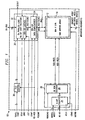
- Figure 1 is a block diagram of a spatial light modulator according to the preferred embodiment of the present invention, including row address and column data loading circuitry for controlling an array of pixels comprising micromirrors;
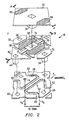
- Figure 2 is an exploded perspective view of one DMD pixel of the array shown in Figure 1, including an elevated micromirror fabricated upon a deflectable yoke, the yoke in turn being supported by a pair of hinges, the hashed areas illustrating the region of electrostatic attraction between the elevated mirror and an elevated address electrode, and between the yoke and the underlying address electrode comprising metal 3 upon the substrate;
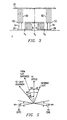
- Figure 3 is an illustration of the electrostatic attraction forces between the mirror and the elevated address electrode, and between the yoke and the underlying address electrode, the yoke and mirror being electrically connected to a bias/reset bus and having the same voltage bias;
- Figure 4 is a sectioned view of a 3 X 3 array of pixels from that array shown in Figure 1, with some of the yokes, elevated address electrodes, and hinge support posts being removed to illustrate the metal 3 layer defining the substrate level address electrodes and the substrate level bias/reset patterns, and also illustrating some of the elevated mirrors being removed to depict the elevated yoke which overlaps portions of the underlying substrate level address electrodes;
- Figure 5 is an illustration of the two stable deflected states of the pixel mirror shown in Figure 4 for deflecting incident light in one of two directions;
- Figure 6 is a cross-sectional view of one pixel of the DMD array of Figure 1 taken along the hinge axis to illustrate the elevated mirror address electrodes and the yoke supported over a pair of substrate address electrodes;
- Figure 7 is also a cross-sectional view such as that of Figure 6, with the yoke and the mirror supported thereon together being rotated to one stable state, whereby the yoke tips land upon a pair of respective landing pads, while the elevated mirror remains proximate but spaced from the elevated mirror address electrodes;
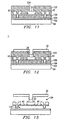
- Figure 8-13 sequentially illustrate the various layers of semiconductor material which are processed to fabricate the pixel of Figure 2 using conventional robust semiconductor processing techniques;
- Figure 14 is an exploded perspective view of an alternative preferred embodiment of the present invention whereby the yoke has only one landing tip defined each side of the torsion axis; and
- Figure 15 is an exploded perspective view of yet another alternative preferred embodiment of the present invention, whereby the yoke has a single landing tip each side of the torsion axis, and wherein the yoke is extended parallel to the torsion axis over the underlying substrate address electrode.
-
- Referring now to Figure 1, a spatial light modulator comprising a digital micromirror device (DMD) is generally shown at 10.
DMD 10 is a single-chip integrated circuit seen to include an 864X 576 micromirror array 12. Array 12 is monolithically fabricated over a 864 X 36memory cell array 16. Each memory cell in the 36 memory cells rows (MR0-MR35) formingmemory cell array 16 is associated with and controlling a dedicated group of sixteen (16)pixels 18, shown in Figure 2. Each memory cell comprises a primary 1-bit static random access memory (SRAM) cell, and a secondary 1-bit SRAM cell fed by the primary cell. There are 864 bit lines BL0-BL863 connected to one of each of the 864 columns of memory cells. Column pixel data is loaded into the addressed primary memory cell row MRn via the associated bit lines BL0-BL863. The primary memory cell is addressed by enabling the associated row write or read enable line, identified as the WDn or RDn , respectively, whereby WPn is connected to the enable input of each primary cell in the row MRn. This pixel data is latched from the primary cell into the respective secondary cell by enabling the global control line MXFRB, the MXFRB line being connected to the enable input of all secondary cells ofarray 16. The secondary memory cell essentially operates as a shadow latch, whereby data can be loaded from the primary memory cell into the secondary memory cell, allowing the primary memory cell to then be subsequently reloaded with new pixel data without effecting the memory cell contents of the secondary memory cell. - Referring now to Figure 2, one
pixel 18 of mirror array 12 is shown. The data of the secondary memory cell is provided to a pair of complementary address electrode lines, each line in turn being connected to one of twoaddress electrodes pixel 18 of array 12.Pixel 18 is seen to include asquare mirror 30 supported upon and elevated above a yoke generally shown at 32 by asupport post 34.Support post 34 extends downward from the center of the mirror, and is attached to the center of theyoke 32 along a torsion axis thereof, as shown, to balance the center of mass ofmirror 30 uponyoke 32.Yoke 32 has a generally butterfly shape, that will be discussed in more detail shortly, and is axially supported along a central axis thereof by a pair of torsion hinges 40. The other end of eachtorsion hinge 40 is attached to and supported by a hingesupport post cap 42 defined on top of a respectivehinge support post 44. A pair of elevatedmirror address electrodes address support post - The address support posts 54 and 56, and the hinge support posts 44 support the
address electrodes yoke 32 away from and above a bias/resetbus 60, and the pair of substrate leveladdress electrode pads mirror 30 andyoke 32 are together rotated about the torsion axis of theyoke 32, defined by thehinges 40, a pair ofyoke tips 58 on the side of theyoke 32 that is deflected land upon and engage the bias/resetbus 60 at thelanding sites 62. - Referring now to Figure 2 in conjunction with Figure 3, a technical advantage of
pixel 18 according to the preferred embodiment of the present invention will be discussed in considerable detail. Rotation ofmirror 30 andyoke 32 can be achieved in one of two directions, to achieve a bistable state and modulate incident light as shown in Figure 5 and will discussed shortly. An address voltage is provided to one of the twoaddress electrodes pads mirror address electrode electrode support post bus 60, and thus toyoke 32 viasupport post 44, post caps 42 and hinges 40, as well as to mirror 30 viasupport 34. The present invention achieves technical advantages by providing an electrostatic force between opposing surfaces at two locations illustrated by the hatched areas in Figure 2. These electrostatic attractive forces are also illustrated at 70, 76, 80 and 82 in Figure 3. - By way of example, if
mirror 30 andyoke 32 are to be rotated counter clockwise as viewed in Figure 2 and Figure 3, a 0 volt potential is provided on address line V a while +5 volts is provided on the complementary address lineV a. Thereafter, a +15 volt potential is provided on the bias line Vb to the bias/resetbus 60 to provide a +15 volt potential onyoke 32 andmirror 30. An electrostatic attraction force from the 20 volt differential is generated betweenaddress electrode 26 and the portion ofyoke 32 above this substrate address electrode, this force being shown generally at 70. The corresponding portion ofyoke 32 that over hangs the addressedelectrode 26 is shown by the hatched portion illustrated at 74. Conversely, if themirror 30 is rotated in a clockwise direction, a 0 volt potential is provided to thecomplement address electrode 28, to generate an attractive force at 76, with the corresponding portion of theyoke 32 over hangingaddress electrode 28 being shown by the hatched region at 78 in Figure.2. - While an electrostatic attraction force is being generated at 70 between one half of
yoke 32 and theunderlying address electrode 26, an electrostatic attractive force is also being generated between theelevated address electrode 50 andmirror 30 as shown at 80 in Figure 3. This electrostatic attractive force is generated by the voltage potential created between the portion ofmirror 30, shown at 82, defined above theelevated address electrode 50. The portion ofmirror 30 overhangingaddress electrode 52 is shown at 84. Therefore, by addressing oneaddress electrode elevated address electrode address electrodes way mirror 30 andyoke 32 will rotate once the +15 volt potential is applied to thebias bus 60, and consequently to theyoke 32 andmirror 30. - Referring to Figure 3, it can be seen that the
elevated address electrodes yoke 32, each being spaced above theaddress electrodes 26 and 28 a distance of about 1 micron. The separation ofmirror 30 above theelevated address electrodes yoke 32 and theaddress electrodes mirror 30 and the correspondingelevated address electrode mirror 30 andyoke 32 to be rotated in the direction toward the address electrodes. - In an alternative embodiment,
elevated electrodes mirror 30 aboveyoke 32 is only about 1 micron to achieve a strong attractive force with the underlying distal lobe ofelectrodes mirror 30 will rotate toward, but will still not engage, the corresponding distal lobe of theaddress electrodes posts 44,yoke 32 andmirror 30 are all of equal potential and the risk of a short is avoided. Thus, limitation to one set of elevated electrodes is not to be inferred. - The address torque (Ta ) is the torque produced by the address voltage alone with the
yoke 32 and themirror 30. This address torque is significantly greater than the address torque generated by previous generation DMD devices for like address voltages and bias potentials. The present invention thus has an improved address margin, which is defined as the difference between the address voltage Va and the potential that is required to ensure the mirror is rotated the proper direction when the bias voltage is applied. - The pixel of the present invention also has an increased latching torque (Tl), which is defined as a measure of the latching torque produced by the bias voltage in the presence of an address voltage tending to rotate (or upset) the mirror to the opposite state. Another dramatically improved performance parameter of the present invention is an increased address-holding torque (Th ), which is defined as a measure of the ability of the address voltage to hold the mirror in its landed state after reset during the time that the bias voltage is off. Another improved feature of the present invention is an increased reset force (Fr ), which is defined as a measure of the tip reaction force produced by a combination of a single-pulse reset and the restoring force produced by the tip of the hinge.
- All four of these performance parameters are substantially improved by the present invention over previous generation DMD devices due to the design of the
yoke 32 generating an electrostatic attractive force with the underlying address electrodes, in combination with electrostatic attractive forces being generated between theelevated mirror 30 and theelevated address electrodes rotatable yoke 32 above theaddress electrodes - The implications of the DMD device of the present invention includes greater address margin, as discussed, less susceptibility to address upset, lower reset voltage requirements, and higher switching speeds which is critical in the operation of the device as a spatial light modulator. With the present design, non- linear hinges can even be incorporated, with stiffer hinges if desired due to improve address margins and latching margins.
- To reduce the possibility of stiction due to Van der Waals forces, the
landing electrodes 60, specifically atregions 62 corresponding with the point of contact fromtips 58 ofyoke 32, can be passivated. By passivating thelanding electrodes 60, the tendency for theyoke 32 to adhere or stick can be decreased. Stiction is an inhibiting force that requires large reset voltages to be applied to reset the mirror to a flat state, or to switch the mirror to the opposing deflectable bistable state. Methods of passivating the landing electrodes are disclosed in commonly assigned U.S. Patent 5,331,454 to Hornbeck, entitled "Low Reset Voltage Process for DMD", and in commonly assigned co-pending Japanese patent application Serial No. 145104/95 entitled "PFPE Coatings for Micro-Mechanical Devices", filed May 9, 1995, laid open #318819/95 with a lay open date of December 8, 1995. To achieve reset of the mirror, and induce deflection of the mirror to the other bistable state, the bias/reset line can be pulsed with a voltage at a frequency corresponding to the resonant frequency of the mirror, which is typically about 5 MHZ, such as disclosed in commonly assigned U.S. Patent 5,096,279, entitled "Spatial Light Modulator and Method". - Turning now to Figure 4, a sectioned perspective view of a 3 X 3 array portion of array 12 is shown to illustrate the fabrication of the metal 3 layer upon the silicon substrate, this metal 3 layer defining the
address electrodes reset buses 60 upon the silicon substrate. Also illustrated is the elevated mirror address electrodes, the post caps, and thehinges supporting yoke 32 above the metal 3 layer. The mirror support post can be seen to be supported by the respective yoke along the torsion axis of the pixel. - Turning now to Figure 5, an optical schematic diagram is shown whereby incident light is seen to be modulated and deflected in one of two directions, depending on whether the mirror is in the "on" or "off" state. When
mirror 30 is in the on state, incident light is reflected to optics including a projector lens, and ultimately focused upon a display screen in the case of a front or rear screen projector, or focused upon a photosensitive surface in the case of a electrophotographic printer. Whenmirror 30 is in the off position, incident light is reflected to a light absorber and away from the darkfield optics. The 20° rotation between the bistable states ofmirror 30 achieves a 40° swing of reflective incident light. Thus, the present invention achieves a high contrast ratio spatial light image, which is critical for use in darkfield optics systems for which the spatial light modulator of the present invention is intended. - Referring now to Figures 6 and 7, a cross sectional view of
pixel 18 taken alone line A-A in Figure 2 is shown with the support posts not being shown. As shown in Figure 6, withyoke 32 andmirror 30 in the undeflected (flat) state,yoke 32 is generally coplanar with theelevated address electrodes address electrodes bias bus 60.Mirror 30 is elevated above the pair ofelevated address electrodes yoke 32 from thesubstrate 64. - Referring to Figure 7, when
yoke 32 andmirror 30 are addressed and rotated in a clockwise direction, as shown, the pair oflanding tips 58 of the addressed half ofyoke 32 land uponportions 62 of reset/bias bus 60. However, theelevated mirror 30, while rotated therewith, remains spaced above and separated from the correspondingelevated address electrode 52. As shown, the moment arm ofyoke 32 is about half the moment arm ofmirror 30 about the torsion axis. The shorter dimension of thelanding yoke 32 compared to themirror 30 reduces the torque necessary to reset a stuck mirror, while using too short a landing yoke can cause additional stress on the torsion hinges. A better understanding of these forces is described in commonly assigned co-pending European patent application Serial No.94120234.3, entitled Multi-Level Digital Micromirror Device", filed December 20, 1994, publication # 0664470, published July 26, 1995. Since theyoke 32 lands upon a pair of opposingtips 58, and is symmetrically designed, a large area ofaddress electrode yoke 32, as shown in Figure 2. In addition, reduced stiction forces between the yoke and thelanding electrode portions 62 has been observed, thus necessitating a lower reset voltage to be applied when changing or resetting the mirror state. - Referring now to Figures 8-13, a detailed discussion of the semiconductor fabrication processes performed to fabricate one
pixel 18 will be described. In each of the Figures 8-13, the section view is taken alone line B-B in Figure 2 for purposes of illustration and clarity, although it is not to scale. - First, referring to Figure 8, a
silicon substrate 64 is processed so as to form the underlying address circuitry including the array ofmemory cells 16, therow address circuitry 20, and the columndata loading circuitry 30. Thereafter,substrate 64 is covered with aprotective oxide layer 102. Next, a third layer of metalization, commonly referred to as M3, is sputter deposited onto the partially processed wafer and being shown at 104. This third metalization layer is patterned and etched to define theaddress electrodes bus 60 shown in Figure 2 and Figure 4. Next, ahinge spacer layer 106 is spin-deposited over the address circuitry and preferably comprises positive photoresist having a thickness of 1 micron. A pair ofvias 110 are opened through thephotoresist layer 106 to facilitate forming the hinge support post, then the layer ofphotoresist 106 is deep UV hardened at a high temperature to prevent flow and bubbling during subsequent processing steps. - Referring now to Figure 9, a
thin hinge layer 112 of metalization is sputter deposited over thephotoresist layer 106 and intovias 110, as shown.Hinge layer 112 preferably has a thickness of about 500 Angstroms, and can be comprised of aluminum, aluminum alloys, titanium tungsten, and other conductive materials well suited for the present invention. The hinge support posts 44 are defined in this step as shown, and are electrically connected to bias/resetbus 60. Also during this step, the pair of electrode support posts 54 and 56 are defined, although not shown, whereby thelayer 112 is sputter deposited in a pair of corresponding vias formed inphotoresist 106, these vias having been formed during the previous step when vias 110 were opened. Thus, the electrode support post and the hinge support post are very similar. The thickness of thephotoresist spacer layer 106 determines the hinge air gap, and thus, determines the mirror rotation angle due to the angular freedom ofyoke 32 until it engages the landing electrodes. - Referring now to Figure 10, a first mask of oxide is plasma-deposited, and patterned in the shape of the hinges 40. Then, a thick metal layer, typically about 3,000 Angstroms thick, of aluminum alloy is deposited. A second mask of oxide is plasma-deposited and then patterned in the shape of the
yoke 32, theelevated electrodes thin hinge layer 112 and the thicker metal layer are then etched to define theaddress electrodes hinges 40, as shown. A single plasma etch is used to define these structures. The two oxide layers act as etch stops, and protect the metal layers beneath them. After completion of the plasma etch process, the oxide etch stops are removed from the thin metal hinges, the thicker metal support posts caps 42, theelectrodes hinges 40, as shown in Figure 10. - Referring now to Figure 11, a thick
mirror spacer layer 122 is spin-deposited over the hinges, electrodes and hinge support caps, and preferably comprises positive photoresist having a thickness of approximately 2 microns. A via 124 is opened in thisphotoresist spacer layer 122 to provide an opening aboveyoke 32, as shown, then the layer ofphotoresist 122 is deep UV hardened. - Referring to Figure 12, a mirror metal layer, comprising of an aluminum alloy and having reflective properties, is then sputter-deposited to a thickness of about 400 nm (4,000 Angstroms). This layer forms both the
mirror support post 34 and themirror 30. A masking oxide layer is then plasma-deposited onto the mirror layer, and patterned in the shape of the rectangular mirrors. The mirror metal layer is then plasma etched to form themirror 30 andsupport post 34, as shown. - The masking oxide layer is typically left in place while the wafer is subsequently processed and sawed to obtain dies.
- Referring to Figure 13, the chips are placed in a plasma etching chamber, where the masking oxide layer and both spacer layers 106 and 122 are plasma etched away, leaving the hinge air gap under the
hinges 40 andyoke 32, as well as a mirror air gap '134 beneath theelevated mirror 30. - Referring now to Figure 14, a perspective exploded view of an alternative embodiment of the present invention is generally shown at 200.
Pixel 200 is seen to be very similar topixel 18 as discussed in regards to Figure 1-13, wherein like numerals refer to like elements. However,pixel 200 has ayoke 202 which is slightly modified to have asingle landing tip 204 each side of the torsion axis, as shown. When rotated, onetip 204 ofyoke 202 will rotate until it engages and lands upon acorresponding landing electrode 208. Theyoke 202 substantially overlaps each of a pair ofaddress pads Hinges 222support yoke 202 from hinge posts 224.Elevated address electrodes yoke 202. - Referring now to Figure 15, yet another alternative preferred embodiment of the present invention is shown at 300.
Pixel 300 is very similar to the embodiment shown in Figure 200, and to thatpixel 18 shown in Figure 1-13, where like numerals refer to like elements.Pixel 300, as shown, also has a single landing tip provided each side of the torsion axis, similar to the embodiment in Figure 14. Ayoke 302 is substantially extended parallel to the torsion axis and over the underlying address electrodes, where a pair ofaddress electrodes yoke 302, and another pair ofaddress electrodes 310 and 312 are provided on the other side of the bias/reset bus 320 which has an X-pattern, as shown. The twoaddress electrodes address electrodes 310 and 312 are electrically tied together. The pairs of address electrodes are electrically connected to the elevatedmirror address electrodes corresponding support post 336, as shown. The areas of electrostatic attraction are shown by the hatched areas of 350, 352, 354, 356, 358 and 360.Hinges 362support yoke 302 fromposts 364. In this embodiment, the bias/reset bus 320 has an X-shape, and bifurcates the pair of address electrodes, as shown. With an X-shape, the bias/reset bus can be easily and conveniently interconnected to adjacent pixels in the metal 3 layer upon the silicon substrate. This may yield a desirable layout for controlling multiple rows of pixels with a common bias/reset bus, and also facilitates the split-reset technique, such as disclosed in commonly assigned European patent application Serial No. 94100308.9, entitled "Pixel Control Circuitry for Spatial Light Modulator", filed January 11, 1994, publication no.0610665, publication date August 17, 1994. The landing cites of the yoke tips are provided along the bias/reset bus, shown at 340. - In summary, a spatial light modulator of the DMD type is disclosed having electrostatic forces generated at two locations to induce deflection of the pixel mirror. First, an attractive force is generated between the yoke and an underlying substrate address electrode. Secondly, an electrostatic force is also generated between the elevated mirror and an elevated address electrode. These electrostatic forces are additive, and realize improved performance parameters over prior generation DMD devices. Since the yoke is separated above the substrate address electrodes by a distance equal to one-half the spacing between the mirror and the elevated address electrodes, an attractive force per unit area is 4 times greater than the force generated between the mirror and the elevated electrodes is achieved. The design of the present invention achieves higher address torques, higher latching torques, higher reset forces, and greater address margins. The pixel is less susceptible to address upset, requires a lower reset voltage, and may eliminate the need for resonant reset and multiple reset pulses. Higher switching speeds are achieved, whereby non-linear and stiffer hinges can be implemented due to the improved performance parameters described. The pixel array can be fabricated with little deviation from the baseline process. Thus, improved performance parameters are achievable with the spatial light modulator of the present invention over previous generations.
Claims (20)
- A spatial light modulator (10), comprising:a substrate (64);addressing circuitry comprising a first portion (26, 28) provided proximate said substrate and a second portion (50, 52) elevated above said substrate;a yoke (32) supported over said addressing circuitry first portion;at least one hinge (40) connected to said yoke (32) and supporting said yoke, said hinge permitting deflection of said yoke; anda pixel (18) elevated above and supported by said yoke, said pixels (18) positioned over said elevated addressing circuitry second portion.
- The spatial light modulator as specified in Claim 1 comprising a pair of said hinges (40) axially supporting said yoke (32) along a yoke axis.
- The spatial light modulator as specified in Claim 1 wherein said yoke (32) has a width less than the width of said pixel (18) and said pixel (18) overlaps said yoke.
- The spatial light modulator as specified in Claim 2 wherein said yoke has a pair of yoke tips (58) on each side of said yoke axis.
- The spatial light modulator as specified in Claim 4 wherein said yoke (32) has a butterfly shape.
- The spatial light modulator as specified in Claim 1 wherein a first spacing is defined between said yoke (32) and said addressing circuitry first portion (26, 28), and a second spacing is defined between said pixel (18) and said addressing circuitry second portion (50, 52), wherein said first spacing is smaller than said second spacing.
- The spatial light modulator as specified in Claim 1 wherein said yoke (32) is in substantially the same plane as said addressing circuitry second portion (50, 52).
- The spatial light modulator as specified in Claim 2 wherein a first pair of opposing surface areas are defined between said yoke (32) and said addressing circuitry first portion (26, 28), and a second pair of opposing surface areas are defined between said pixel (18) and said addressing circuitry second portion (50, 52), said second pair of opposing surface areas being laterally defined a greater distance from said yoke axis than is said first pair of opposing surface areas from said yoke axis.
- The spatial light modulator as specified in Claim 1 further comprising a bias/reset bus (60), constructed on said substrate (64) and electrically connected to said pixel (18).
- The spatial light modulator as specified in Claim 1 wherein said hinge (40) is in substantially the same plane as said yoke (32).
- The spatial light modulator as specified in Claim 1 further comprising control circuitry coupled to said addressing circuitry (26, 28, 50, 52), said control circuitry providing address data to said addressing circuitry first portion and said second portion to cause deflection of said pixel (18).
- The spatial light modulator as specified in Claim 2 further comprising control circuitry coupled to said addressing circuitry, said control circuitry providing address data to one of said addressing circuitry first portions (26, 28) to cause deflection of said yoke (32) toward said addressed first portion.
- The spatial light modulator as specified in Claim 1 further comprising a support post (34) connected to and supporting said hinge (40).
- The spatial light modulator as specified in Claim 1 wherein said addressing circuitry first portion (26, 28) and said second portion (50, 52) are electronically connected to one another.
- The spatial light modulator as specified in Claim 1 wherein said pixel (18) is a mirror (30).
- The spatial light modulator as specified in Claim 15 wherein said mirror (30) has a rectangular shape.
- The spatial light modulator as specified in Claim 16 wherein said mirror (30) has edges geometrically oriented at 45 with respect to said hinge.
- The spatial light modulator as specified in Claim 1 wherein said second portiony resides above a plane defined by said first portion (26, 28).
- A display device including a spatial light modulator (10) as defined in Claim 1.
- A printing device including a spatial light modulator (10) as defined in Claim 1.
Applications Claiming Priority (2)
| Application Number | Priority Date | Filing Date | Title |
|---|---|---|---|
| US424021 | 1995-04-18 | ||
| US08/424,021 US5535047A (en) | 1995-04-18 | 1995-04-18 | Active yoke hidden hinge digital micromirror device |
Publications (3)
| Publication Number | Publication Date |
|---|---|
| EP0738910A2 EP0738910A2 (en) | 1996-10-23 |
| EP0738910A3 EP0738910A3 (en) | 2002-11-13 |
| EP0738910B1 true EP0738910B1 (en) | 2005-01-26 |
Family
ID=23681129
Family Applications (1)
| Application Number | Title | Priority Date | Filing Date |
|---|---|---|---|
| EP96106099A Expired - Lifetime EP0738910B1 (en) | 1995-04-18 | 1996-04-18 | Improvements relating to a digital micromirror device |
Country Status (8)
| Country | Link |
|---|---|
| US (1) | US5535047A (en) |
| EP (1) | EP0738910B1 (en) |
| JP (1) | JP3851679B2 (en) |
| KR (1) | KR100416679B1 (en) |
| CN (1) | CN1160218A (en) |
| CA (1) | CA2173637C (en) |
| DE (1) | DE69634222T2 (en) |
| TW (1) | TW295631B (en) |
Families Citing this family (345)
| Publication number | Priority date | Publication date | Assignee | Title |
|---|---|---|---|---|
| US6674562B1 (en) | 1994-05-05 | 2004-01-06 | Iridigm Display Corporation | Interferometric modulation of radiation |
| US6426013B1 (en) | 1993-10-18 | 2002-07-30 | Xros, Inc. | Method for fabricating micromachined members coupled for relative rotation |
| US6044705A (en) * | 1993-10-18 | 2000-04-04 | Xros, Inc. | Micromachined members coupled for relative rotation by torsion bars |
| US6467345B1 (en) | 1993-10-18 | 2002-10-22 | Xros, Inc. | Method of operating micromachined members coupled for relative rotation |
| US8014059B2 (en) | 1994-05-05 | 2011-09-06 | Qualcomm Mems Technologies, Inc. | System and method for charge control in a MEMS device |
| US5650881A (en) * | 1994-11-02 | 1997-07-22 | Texas Instruments Incorporated | Support post architecture for micromechanical devices |
| US5703728A (en) * | 1994-11-02 | 1997-12-30 | Texas Instruments Incorporated | Support post architecture for micromechanical devices |
| KR100213281B1 (en) * | 1994-10-31 | 1999-08-02 | 전주범 | The lightpath modulation device |
| US5671083A (en) * | 1995-02-02 | 1997-09-23 | Texas Instruments Incorporated | Spatial light modulator with buried passive charge storage cell array |
| US6969635B2 (en) * | 2000-12-07 | 2005-11-29 | Reflectivity, Inc. | Methods for depositing, releasing and packaging micro-electromechanical devices on wafer substrates |
| US6046840A (en) * | 1995-06-19 | 2000-04-04 | Reflectivity, Inc. | Double substrate reflective spatial light modulator with self-limiting micro-mechanical elements |
| US5835256A (en) * | 1995-06-19 | 1998-11-10 | Reflectivity, Inc. | Reflective spatial light modulator with encapsulated micro-mechanical elements |
| US5739941A (en) * | 1995-07-20 | 1998-04-14 | Texas Instruments Incorporated | Non-linear hinge for micro-mechanical device |
| US6172496B1 (en) * | 1995-09-18 | 2001-01-09 | James P. Karins | Static event detection/protection device |
| US5867202A (en) * | 1995-12-15 | 1999-02-02 | Texas Instruments Incorporated | Micromechanical devices with spring tips |
| US6686291B1 (en) | 1996-05-24 | 2004-02-03 | Texas Instruments Incorporated | Undercut process with isotropic plasma etching at package level |
| US5754332A (en) * | 1996-06-27 | 1998-05-19 | Xerox Corporation | Monolayer gyricon display |
| US6055091A (en) * | 1996-06-27 | 2000-04-25 | Xerox Corporation | Twisting-cylinder display |
| US5825529A (en) * | 1996-06-27 | 1998-10-20 | Xerox Corporation | Gyricon display with no elastomer substrate |
| US5914805A (en) * | 1996-06-27 | 1999-06-22 | Xerox Corporation | Gyricon display with interstitially packed particles |
| US5922268A (en) * | 1997-10-30 | 1999-07-13 | Xerox Corporation | Method of manufacturing a twisting cylinder display using multiple chromatic values |
| US5894367A (en) * | 1996-09-13 | 1999-04-13 | Xerox Corporation | Twisting cylinder display using multiple chromatic values |
| US5904790A (en) * | 1997-10-30 | 1999-05-18 | Xerox Corporation | Method of manufacturing a twisting cylinder display using multiple chromatic values |
| US5771116A (en) * | 1996-10-21 | 1998-06-23 | Texas Instruments Incorporated | Multiple bias level reset waveform for enhanced DMD control |
| US7471444B2 (en) | 1996-12-19 | 2008-12-30 | Idc, Llc | Interferometric modulation of radiation |
| US6028689A (en) * | 1997-01-24 | 2000-02-22 | The United States Of America As Represented By The Secretary Of The Air Force | Multi-motion micromirror |
| DE19710597C1 (en) * | 1997-03-14 | 1998-07-23 | Block Augenoptische Und Ophtha | Arrangement for generating illuminated region with high, locally variable energy density for eye surgery |
| US5817569A (en) * | 1997-05-08 | 1998-10-06 | Texas Instruments Incorporated | Method of reducing wafer particles after partial saw |
| DE69806846T2 (en) * | 1997-05-08 | 2002-12-12 | Texas Instruments Inc | Improvements for spatial light modulators |
| US5903383A (en) * | 1997-05-19 | 1999-05-11 | The Charles Stark Draper Laboratory Inc. | Electrostatic memory micromirror display system |
| US5808780A (en) * | 1997-06-09 | 1998-09-15 | Texas Instruments Incorporated | Non-contacting micromechanical optical switch |
| US5790297A (en) | 1997-06-26 | 1998-08-04 | Xerox Corporation | Optical row displacement for a fault tolerant projective display |
| US5774254A (en) * | 1997-06-26 | 1998-06-30 | Xerox Corporation | Fault tolerant light modulator display system |
| DE19733370C2 (en) * | 1997-08-01 | 2000-07-06 | Agfa Gevaert Ag | Apparatus and method for copying images onto light-sensitive material |
| US5867302A (en) * | 1997-08-07 | 1999-02-02 | Sandia Corporation | Bistable microelectromechanical actuator |
| DE19757197A1 (en) * | 1997-12-22 | 1999-06-24 | Bosch Gmbh Robert | Manufacturing method for micromechanical device, esp. for resonant oscillating mirror device |
| US5976428A (en) * | 1998-01-09 | 1999-11-02 | Xerox Corporation | Method and apparatus for controlling formation of two-color balls for a twisting ball display |
| US5900192A (en) * | 1998-01-09 | 1999-05-04 | Xerox Corporation | Method and apparatus for fabricating very small two-color balls for a twisting ball display |
| EP1054726B1 (en) * | 1998-02-11 | 2003-07-30 | University of Houston, Office of Technology Transfer | Apparatus for chemical and biochemical reactions using photo-generated reagents |
| US20040035690A1 (en) * | 1998-02-11 | 2004-02-26 | The Regents Of The University Of Michigan | Method and apparatus for chemical and biochemical reactions using photo-generated reagents |
| IL137901A (en) | 1998-02-23 | 2004-07-25 | Wisconsin Alumni Res Found | Method and apparatus for synthesis of arrays of dna probes |
| US6206290B1 (en) | 1998-03-06 | 2001-03-27 | Symbol Technologies, Inc. | Control system for oscillating optical element in scanners |
| KR100703140B1 (en) | 1998-04-08 | 2007-04-05 | 이리다임 디스플레이 코포레이션 | Interferometric modulation and its manufacturing method |
| US8928967B2 (en) | 1998-04-08 | 2015-01-06 | Qualcomm Mems Technologies, Inc. | Method and device for modulating light |
| US6271957B1 (en) * | 1998-05-29 | 2001-08-07 | Affymetrix, Inc. | Methods involving direct write optical lithography |
| DE19824709A1 (en) * | 1998-06-03 | 1999-12-09 | Bundesdruckerei Gmbh | Producing luminance distribution array from rays projected onto medium using digital array radiation processors |
| US6962419B2 (en) | 1998-09-24 | 2005-11-08 | Reflectivity, Inc | Micromirror elements, package for the micromirror elements, and projection system therefor |
| US6529310B1 (en) | 1998-09-24 | 2003-03-04 | Reflectivity, Inc. | Deflectable spatial light modulator having superimposed hinge and deflectable element |
| US6031657A (en) * | 1998-10-15 | 2000-02-29 | Memsolutions, Inc. | Membrane-actuated charge controlled mirror (CCM) projection display |
| US5991066A (en) * | 1998-10-15 | 1999-11-23 | Memsolutions, Inc. | Membrane-actuated charge controlled mirror |
| US6123985A (en) * | 1998-10-28 | 2000-09-26 | Solus Micro Technologies, Inc. | Method of fabricating a membrane-actuated charge controlled mirror (CCM) |
| US6700606B1 (en) * | 1999-06-09 | 2004-03-02 | Activcard Ireland Limited | Micromirror optical imager |
| US6671005B1 (en) | 1999-06-21 | 2003-12-30 | Altman Stage Lighting Company | Digital micromirror stage lighting system |
| WO2003007049A1 (en) | 1999-10-05 | 2003-01-23 | Iridigm Display Corporation | Photonic mems and structures |
| US6396619B1 (en) | 2000-01-28 | 2002-05-28 | Reflectivity, Inc. | Deflectable spatial light modulator having stopping mechanisms |
| US6741383B2 (en) | 2000-08-11 | 2004-05-25 | Reflectivity, Inc. | Deflectable micromirrors with stopping mechanisms |
| US6529311B1 (en) * | 1999-10-28 | 2003-03-04 | The Trustees Of Boston University | MEMS-based spatial-light modulator with integrated electronics |
| US6412972B1 (en) | 1999-12-10 | 2002-07-02 | Altman Stage Lighting Company | Digital light protection apparatus with digital micromirror device and rotatable housing |
| US6440252B1 (en) | 1999-12-17 | 2002-08-27 | Xerox Corporation | Method for rotatable element assembly |
| US6466358B2 (en) * | 1999-12-30 | 2002-10-15 | Texas Instruments Incorporated | Analog pulse width modulation cell for digital micromechanical device |
| US6545671B1 (en) | 2000-03-02 | 2003-04-08 | Xerox Corporation | Rotating element sheet material with reversible highlighting |
| US6498674B1 (en) | 2000-04-14 | 2002-12-24 | Xerox Corporation | Rotating element sheet material with generalized containment structure |
| FR2807844B1 (en) * | 2000-04-17 | 2003-05-16 | Commissariat Energie Atomique | MOBILE PIECE OPTICAL SWITCH AND ITS PRODUCTION METHOD, AND OPTICAL BREWING DEVICE USING THE OPTICAL SWITCH |
| KR100708077B1 (en) * | 2000-05-01 | 2007-04-16 | 삼성전자주식회사 | Micro-mirro device for image display apparatus |
| US6504525B1 (en) | 2000-05-03 | 2003-01-07 | Xerox Corporation | Rotating element sheet material with microstructured substrate and method of use |
| US6813053B1 (en) * | 2000-05-19 | 2004-11-02 | The Regents Of The University Of California | Apparatus and method for controlled cantilever motion through torsional beams and a counterweight |
| US6781742B2 (en) * | 2000-07-11 | 2004-08-24 | Semiconductor Energy Laboratory Co., Ltd. | Digital micromirror device and method of driving digital micromirror device |
| US7099065B2 (en) * | 2000-08-03 | 2006-08-29 | Reflectivity, Inc. | Micromirrors with OFF-angle electrodes and stops |
| US6567163B1 (en) | 2000-08-17 | 2003-05-20 | Able Signal Company Llc | Microarray detector and synthesizer |
| US6545758B1 (en) | 2000-08-17 | 2003-04-08 | Perry Sandstrom | Microarray detector and synthesizer |
| US7172296B2 (en) * | 2000-08-30 | 2007-02-06 | Reflectivity, Inc | Projection display |
| US6522454B2 (en) | 2000-09-29 | 2003-02-18 | Texas Instruments Incorporated | Hidden hinge digital micromirror device with improved manufacturing yield and improved contrast ratio |
| US6962771B1 (en) * | 2000-10-13 | 2005-11-08 | Taiwan Semiconductor Manufacturing Company, Ltd. | Dual damascene process |
| AU2002224007A1 (en) * | 2000-11-22 | 2002-06-03 | Flixel Ltd. | Microelectromechanical display devices |
| US6614576B2 (en) * | 2000-12-15 | 2003-09-02 | Texas Instruments Incorporated | Surface micro-planarization for enhanced optical efficiency and pixel performance in SLM devices |
| US6524500B2 (en) | 2000-12-28 | 2003-02-25 | Xerox Corporation | Method for making microencapsulated gyricon beads |
| US6690350B2 (en) | 2001-01-11 | 2004-02-10 | Xerox Corporation | Rotating element sheet material with dual vector field addressing |
| US6480320B2 (en) | 2001-02-07 | 2002-11-12 | Transparent Optical, Inc. | Microelectromechanical mirror and mirror array |
| US6585378B2 (en) | 2001-03-20 | 2003-07-01 | Eastman Kodak Company | Digital cinema projector |
| US7023606B2 (en) * | 2001-08-03 | 2006-04-04 | Reflectivity, Inc | Micromirror array for projection TV |
| JP3750574B2 (en) * | 2001-08-16 | 2006-03-01 | 株式会社デンソー | Thin film electromagnet and switching element using the same |
| KR100398310B1 (en) | 2001-09-13 | 2003-09-19 | 한국과학기술원 | Micromirror device using interdigitated cantilevers and its applications |
| US6844952B2 (en) * | 2001-09-18 | 2005-01-18 | Vitesse Semiconductor Corporation | Actuator-controlled mirror with Z-stop mechanism |
| US6809851B1 (en) * | 2001-10-24 | 2004-10-26 | Decicon, Inc. | MEMS driver |
| US6699570B2 (en) | 2001-11-06 | 2004-03-02 | Xerox Corporation | Colored cyber toner using multicolored gyricon spheres |
| US6885492B2 (en) | 2001-11-08 | 2005-04-26 | Imaginative Optics, Inc. | Spatial light modulator apparatus |
| EP1315016B1 (en) * | 2001-11-21 | 2006-08-23 | Texas Instruments Incorporated | Yokeless hidden hinge digital micromirror device |
| CN1608221A (en) * | 2001-12-03 | 2005-04-20 | 弗利克赛尔公司 | Display devices |
| US7116459B2 (en) * | 2001-12-27 | 2006-10-03 | Texas Instruments Incorporated | Field diode detection of excess light conditions for spatial light modulator |
| US7061561B2 (en) * | 2002-01-07 | 2006-06-13 | Moxtek, Inc. | System for creating a patterned polarization compensator |
| US6909473B2 (en) * | 2002-01-07 | 2005-06-21 | Eastman Kodak Company | Display apparatus and method |
| US6808269B2 (en) * | 2002-01-16 | 2004-10-26 | Eastman Kodak Company | Projection apparatus using spatial light modulator |
| US6574033B1 (en) | 2002-02-27 | 2003-06-03 | Iridigm Display Corporation | Microelectromechanical systems device and method for fabricating same |
| US20030187330A1 (en) * | 2002-03-28 | 2003-10-02 | Fuji Photo Optical Co., Ltd. | Electronic endoscope apparatus using micromirror device |
| US7018268B2 (en) * | 2002-04-09 | 2006-03-28 | Strasbaugh | Protection of work piece during surface processing |
| WO2003086955A1 (en) * | 2002-04-12 | 2003-10-23 | Fraunhofer-Gesellschaft zur Förderung der angewandten Forschung e.V. | Method and device for operating a micromechanical element |
| US6996292B1 (en) | 2002-04-18 | 2006-02-07 | Sandia Corporation | Staring 2-D hadamard transform spectral imager |
| US6676260B2 (en) | 2002-04-25 | 2004-01-13 | Eastman Kodak Company | Projection apparatus using spatial light modulator with relay lens and dichroic combiner |
| US6648475B1 (en) | 2002-05-20 | 2003-11-18 | Eastman Kodak Company | Method and apparatus for increasing color gamut of a display |
| US7034984B2 (en) * | 2002-06-19 | 2006-04-25 | Miradia Inc. | Fabrication of a high fill ratio reflective spatial light modulator with hidden hinge |
| US6992810B2 (en) * | 2002-06-19 | 2006-01-31 | Miradia Inc. | High fill ratio reflective spatial light modulator with hidden hinge |
| US20040004753A1 (en) * | 2002-06-19 | 2004-01-08 | Pan Shaoher X. | Architecture of a reflective spatial light modulator |
| US20040069742A1 (en) * | 2002-06-19 | 2004-04-15 | Pan Shaoher X. | Fabrication of a reflective spatial light modulator |
| US20030234994A1 (en) * | 2002-06-19 | 2003-12-25 | Pan Shaoher X. | Reflective spatial light modulator |
| US7206110B2 (en) * | 2002-06-19 | 2007-04-17 | Miradia Inc. | Memory cell dual protection |
| US6736514B2 (en) | 2002-06-21 | 2004-05-18 | Eastman Kodak Company | Imaging apparatus for increased color gamut using dual spatial light modulators |
| US6843574B2 (en) * | 2002-08-20 | 2005-01-18 | Intel Corporation | Gimbaled micromechanical rotation system |
| US6809873B2 (en) * | 2002-09-09 | 2004-10-26 | Eastman Kodak Company | Color illumination system for spatial light modulators using multiple double telecentric relays |
| JP2004101826A (en) * | 2002-09-09 | 2004-04-02 | Fuji Photo Optical Co Ltd | Optical system for projector, and projector device using same |
| US7781850B2 (en) | 2002-09-20 | 2010-08-24 | Qualcomm Mems Technologies, Inc. | Controlling electromechanical behavior of structures within a microelectromechanical systems device |
| US6733144B2 (en) | 2002-09-27 | 2004-05-11 | Intel Corporation | Shock protectors for micro-mechanical systems |
| US6825968B2 (en) * | 2002-10-11 | 2004-11-30 | Exajoule, Llc | Micromirror systems with electrodes configured for sequential mirror attraction |
| US6870659B2 (en) * | 2002-10-11 | 2005-03-22 | Exajoule, Llc | Micromirror systems with side-supported mirrors and concealed flexure members |
| US6769772B2 (en) * | 2002-10-11 | 2004-08-03 | Eastman Kodak Company | Six color display apparatus having increased color gamut |
| US6798560B2 (en) * | 2002-10-11 | 2004-09-28 | Exajoula, Llc | Micromirror systems with open support structures |
| US6802613B2 (en) * | 2002-10-16 | 2004-10-12 | Eastman Kodak Company | Broad gamut color display apparatus using an electromechanical grating device |
| US6807010B2 (en) * | 2002-11-13 | 2004-10-19 | Eastman Kodak Company | Projection display apparatus having both incoherent and laser light sources |
| US6947459B2 (en) * | 2002-11-25 | 2005-09-20 | Eastman Kodak Company | Organic vertical cavity laser and imaging system |
| US7405860B2 (en) * | 2002-11-26 | 2008-07-29 | Texas Instruments Incorporated | Spatial light modulators with light blocking/absorbing areas |
| US20040150794A1 (en) * | 2003-01-30 | 2004-08-05 | Eastman Kodak Company | Projector with camcorder defeat |
| FR2850762A1 (en) * | 2003-01-31 | 2004-08-06 | Commissariat Energie Atomique | OBJECT ORIENTATION DEVICE |
| US7042622B2 (en) * | 2003-10-30 | 2006-05-09 | Reflectivity, Inc | Micromirror and post arrangements on substrates |
| US6885494B2 (en) * | 2003-02-12 | 2005-04-26 | Reflectivity, Inc. | High angle micro-mirrors and processes |
| US7436573B2 (en) * | 2003-02-12 | 2008-10-14 | Texas Instruments Incorporated | Electrical connections in microelectromechanical devices |
| WO2004074167A2 (en) * | 2003-02-20 | 2004-09-02 | Technion Research & Development Foundation Ltd. | A device and method for stacked multi-level uncoupled electrostatic actuators |
| US6900922B2 (en) * | 2003-02-24 | 2005-05-31 | Exajoule, Llc | Multi-tilt micromirror systems with concealed hinge structures |
| US6906848B2 (en) * | 2003-02-24 | 2005-06-14 | Exajoule, Llc | Micromirror systems with concealed multi-piece hinge structures |
| US6758565B1 (en) * | 2003-03-20 | 2004-07-06 | Eastman Kodak Company | Projection apparatus using telecentric optics |
| US6914711B2 (en) * | 2003-03-22 | 2005-07-05 | Active Optical Networks, Inc. | Spatial light modulator with hidden comb actuator |
| US7375874B1 (en) | 2003-03-22 | 2008-05-20 | Active Optical Mems Inc. | Light modulator with integrated drive and control circuitry |
| US7015885B2 (en) * | 2003-03-22 | 2006-03-21 | Active Optical Networks, Inc. | MEMS devices monolithically integrated with drive and control circuitry |
| US7221759B2 (en) * | 2003-03-27 | 2007-05-22 | Eastman Kodak Company | Projector with enhanced security camcorder defeat |
| US7095546B2 (en) * | 2003-04-24 | 2006-08-22 | Metconnex Canada Inc. | Micro-electro-mechanical-system two dimensional mirror with articulated suspension structures for high fill factor arrays |
| TW570896B (en) | 2003-05-26 | 2004-01-11 | Prime View Int Co Ltd | A method for fabricating an interference display cell |
| KR20060014434A (en) * | 2003-06-02 | 2006-02-15 | 미라디아 인크. | High fill ratio reflective spatial light modulator with hidden hinge |
| US6839181B1 (en) * | 2003-06-25 | 2005-01-04 | Eastman Kodak Company | Display apparatus |
| US7131762B2 (en) * | 2003-07-25 | 2006-11-07 | Texas Instruments Incorporated | Color rendering of illumination light in display systems |
| US7212359B2 (en) * | 2003-07-25 | 2007-05-01 | Texas Instruments Incorporated | Color rendering of illumination light in display systems |
| US20050094241A1 (en) * | 2003-11-01 | 2005-05-05 | Fusao Ishii | Electromechanical micromirror devices and methods of manufacturing the same |
| JP4406549B2 (en) | 2003-09-22 | 2010-01-27 | 富士フイルム株式会社 | Light modulation element, light modulation array element, and exposure apparatus using the same |
| JP2005121906A (en) | 2003-10-16 | 2005-05-12 | Fuji Photo Film Co Ltd | Reflection type optical modulation array element and exposure device |
| US8238019B2 (en) * | 2003-11-01 | 2012-08-07 | Silicon Quest Kabushiki-Kaisha | Projection apparatus with coherent light source |
| US7026695B2 (en) * | 2003-11-19 | 2006-04-11 | Miradia Inc. | Method and apparatus to reduce parasitic forces in electro-mechanical systems |
| US7295726B1 (en) * | 2003-12-02 | 2007-11-13 | Adriatic Research Institute | Gimbal-less micro-electro-mechanical-system tip-tilt and tip-tilt-piston actuators and a method for forming the same |
| US7428353B1 (en) | 2003-12-02 | 2008-09-23 | Adriatic Research Institute | MEMS device control with filtered voltage signal shaping |
| US7161728B2 (en) | 2003-12-09 | 2007-01-09 | Idc, Llc | Area array modulation and lead reduction in interferometric modulators |
| US7142346B2 (en) | 2003-12-09 | 2006-11-28 | Idc, Llc | System and method for addressing a MEMS display |
| US6902277B1 (en) | 2004-01-06 | 2005-06-07 | Eastman Kodak Company | Housing for a spatial light modulator |
| JP4162606B2 (en) | 2004-01-26 | 2008-10-08 | 富士フイルム株式会社 | Light modulation element, light modulation element array, and image forming apparatus |
| US7333260B2 (en) * | 2004-08-09 | 2008-02-19 | Stereo Display, Inc. | Two-dimensional image projection system |
| US7706050B2 (en) | 2004-03-05 | 2010-04-27 | Qualcomm Mems Technologies, Inc. | Integrated modulator illumination |
| WO2005094087A1 (en) * | 2004-03-19 | 2005-10-06 | Thomson Licensing | Video processor alignment clamping spring |
| US7304782B2 (en) | 2004-03-24 | 2007-12-04 | Fujifilm Corporation | Driving method of spatial light modulator array, spatial light modulator array, and image forming apparatus |
| US7720148B2 (en) * | 2004-03-26 | 2010-05-18 | The Hong Kong University Of Science And Technology | Efficient multi-frame motion estimation for video compression |
| US7068409B2 (en) * | 2004-03-31 | 2006-06-27 | Lucent Technologies Inc. | Tip-tilt-piston actuator |
| US7449284B2 (en) | 2004-05-11 | 2008-11-11 | Miradia Inc. | Method and structure for fabricating mechanical mirror structures using backside alignment techniques |
| US20050255666A1 (en) * | 2004-05-11 | 2005-11-17 | Miradia Inc. | Method and structure for aligning mechanical based device to integrated circuits |
| US7164520B2 (en) | 2004-05-12 | 2007-01-16 | Idc, Llc | Packaging for an interferometric modulator |
| US7787170B2 (en) * | 2004-06-15 | 2010-08-31 | Texas Instruments Incorporated | Micromirror array assembly with in-array pillars |
| US7042619B1 (en) * | 2004-06-18 | 2006-05-09 | Miradia Inc. | Mirror structure with single crystal silicon cross-member |
| US7113322B2 (en) * | 2004-06-23 | 2006-09-26 | Reflectivity, Inc | Micromirror having offset addressing electrode |
| US7483126B2 (en) * | 2004-06-23 | 2009-01-27 | Texas Instruments Incorporated | Performance analyses of micromirror devices |
| US7068417B2 (en) * | 2004-07-28 | 2006-06-27 | Miradia Inc. | Method and apparatus for a reflective spatial light modulator with a flexible pedestal |
| US7889163B2 (en) | 2004-08-27 | 2011-02-15 | Qualcomm Mems Technologies, Inc. | Drive method for MEMS devices |
| US7560299B2 (en) | 2004-08-27 | 2009-07-14 | Idc, Llc | Systems and methods of actuating MEMS display elements |
| US7551159B2 (en) | 2004-08-27 | 2009-06-23 | Idc, Llc | System and method of sensing actuation and release voltages of an interferometric modulator |
| US7499208B2 (en) | 2004-08-27 | 2009-03-03 | Udc, Llc | Current mode display driver circuit realization feature |
| US7515147B2 (en) | 2004-08-27 | 2009-04-07 | Idc, Llc | Staggered column drive circuit systems and methods |
| US7602375B2 (en) | 2004-09-27 | 2009-10-13 | Idc, Llc | Method and system for writing data to MEMS display elements |
| US7920135B2 (en) | 2004-09-27 | 2011-04-05 | Qualcomm Mems Technologies, Inc. | Method and system for driving a bi-stable display |
| US7719500B2 (en) | 2004-09-27 | 2010-05-18 | Qualcomm Mems Technologies, Inc. | Reflective display pixels arranged in non-rectangular arrays |
| US7944599B2 (en) | 2004-09-27 | 2011-05-17 | Qualcomm Mems Technologies, Inc. | Electromechanical device with optical function separated from mechanical and electrical function |
| US20060076634A1 (en) | 2004-09-27 | 2006-04-13 | Lauren Palmateer | Method and system for packaging MEMS devices with incorporated getter |
| US7710629B2 (en) | 2004-09-27 | 2010-05-04 | Qualcomm Mems Technologies, Inc. | System and method for display device with reinforcing substance |
| US7136213B2 (en) | 2004-09-27 | 2006-11-14 | Idc, Llc | Interferometric modulators having charge persistence |
| US8878825B2 (en) | 2004-09-27 | 2014-11-04 | Qualcomm Mems Technologies, Inc. | System and method for providing a variable refresh rate of an interferometric modulator display |
| US7369296B2 (en) | 2004-09-27 | 2008-05-06 | Idc, Llc | Device and method for modifying actuation voltage thresholds of a deformable membrane in an interferometric modulator |
| US7675669B2 (en) | 2004-09-27 | 2010-03-09 | Qualcomm Mems Technologies, Inc. | Method and system for driving interferometric modulators |
| US7420725B2 (en) | 2004-09-27 | 2008-09-02 | Idc, Llc | Device having a conductive light absorbing mask and method for fabricating same |
| US7626581B2 (en) | 2004-09-27 | 2009-12-01 | Idc, Llc | Device and method for display memory using manipulation of mechanical response |
| US7843410B2 (en) | 2004-09-27 | 2010-11-30 | Qualcomm Mems Technologies, Inc. | Method and device for electrically programmable display |
| US7701631B2 (en) | 2004-09-27 | 2010-04-20 | Qualcomm Mems Technologies, Inc. | Device having patterned spacers for backplates and method of making the same |
| US7545550B2 (en) | 2004-09-27 | 2009-06-09 | Idc, Llc | Systems and methods of actuating MEMS display elements |
| WO2006037044A1 (en) | 2004-09-27 | 2006-04-06 | Idc, Llc | Method and device for multistate interferometric light modulation |
| US8008736B2 (en) | 2004-09-27 | 2011-08-30 | Qualcomm Mems Technologies, Inc. | Analog interferometric modulator device |
| US7417783B2 (en) | 2004-09-27 | 2008-08-26 | Idc, Llc | Mirror and mirror layer for optical modulator and method |
| US8310441B2 (en) | 2004-09-27 | 2012-11-13 | Qualcomm Mems Technologies, Inc. | Method and system for writing data to MEMS display elements |
| US7692839B2 (en) | 2004-09-27 | 2010-04-06 | Qualcomm Mems Technologies, Inc. | System and method of providing MEMS device with anti-stiction coating |
| US7424198B2 (en) | 2004-09-27 | 2008-09-09 | Idc, Llc | Method and device for packaging a substrate |
| US7724993B2 (en) | 2004-09-27 | 2010-05-25 | Qualcomm Mems Technologies, Inc. | MEMS switches with deforming membranes |
| US7583429B2 (en) | 2004-09-27 | 2009-09-01 | Idc, Llc | Ornamental display device |
| US7653371B2 (en) | 2004-09-27 | 2010-01-26 | Qualcomm Mems Technologies, Inc. | Selectable capacitance circuit |
| US7813026B2 (en) | 2004-09-27 | 2010-10-12 | Qualcomm Mems Technologies, Inc. | System and method of reducing color shift in a display |
| US7893919B2 (en) | 2004-09-27 | 2011-02-22 | Qualcomm Mems Technologies, Inc. | Display region architectures |
| US7289259B2 (en) | 2004-09-27 | 2007-10-30 | Idc, Llc | Conductive bus structure for interferometric modulator array |
| US7936497B2 (en) | 2004-09-27 | 2011-05-03 | Qualcomm Mems Technologies, Inc. | MEMS device having deformable membrane characterized by mechanical persistence |
| US7355780B2 (en) | 2004-09-27 | 2008-04-08 | Idc, Llc | System and method of illuminating interferometric modulators using backlighting |
| US7808703B2 (en) | 2004-09-27 | 2010-10-05 | Qualcomm Mems Technologies, Inc. | System and method for implementation of interferometric modulator displays |
| US7446927B2 (en) | 2004-09-27 | 2008-11-04 | Idc, Llc | MEMS switch with set and latch electrodes |
| US7916103B2 (en) * | 2004-09-27 | 2011-03-29 | Qualcomm Mems Technologies, Inc. | System and method for display device with end-of-life phenomena |
| US8124434B2 (en) | 2004-09-27 | 2012-02-28 | Qualcomm Mems Technologies, Inc. | Method and system for packaging a display |
| US7372613B2 (en) | 2004-09-27 | 2008-05-13 | Idc, Llc | Method and device for multistate interferometric light modulation |
| US7684104B2 (en) | 2004-09-27 | 2010-03-23 | Idc, Llc | MEMS using filler material and method |
| US7679627B2 (en) | 2004-09-27 | 2010-03-16 | Qualcomm Mems Technologies, Inc. | Controller and driver features for bi-stable display |
| US7668415B2 (en) | 2004-09-27 | 2010-02-23 | Qualcomm Mems Technologies, Inc. | Method and device for providing electronic circuitry on a backplate |
| US7345805B2 (en) | 2004-09-27 | 2008-03-18 | Idc, Llc | Interferometric modulator array with integrated MEMS electrical switches |
| US7310179B2 (en) | 2004-09-27 | 2007-12-18 | Idc, Llc | Method and device for selective adjustment of hysteresis window |
| US7532195B2 (en) | 2004-09-27 | 2009-05-12 | Idc, Llc | Method and system for reducing power consumption in a display |
| CN1769945A (en) | 2004-09-30 | 2006-05-10 | 富士胶片株式会社 | Microelectromechanical modulation device and microelectromechanical modulation device array, and image forming apparatus |
| US7092143B2 (en) * | 2004-10-19 | 2006-08-15 | Reflectivity, Inc | Micromirror array device and a method for making the same |
| US7158279B2 (en) * | 2004-10-19 | 2007-01-02 | Texas Instruments Incorporated | Spatial light modulators with non-uniform pixels |
| US7961393B2 (en) | 2004-12-06 | 2011-06-14 | Moxtek, Inc. | Selectively absorptive wire-grid polarizer |
| US7800823B2 (en) | 2004-12-06 | 2010-09-21 | Moxtek, Inc. | Polarization device to polarize and further control light |
| US7570424B2 (en) | 2004-12-06 | 2009-08-04 | Moxtek, Inc. | Multilayer wire-grid polarizer |
| US7106492B2 (en) * | 2004-12-21 | 2006-09-12 | Texas Instruments Incorporated | Bias voltage routing scheme for a digital micro-mirror device |
| US7172921B2 (en) | 2005-01-03 | 2007-02-06 | Miradia Inc. | Method and structure for forming an integrated spatial light modulator |
| US8207004B2 (en) | 2005-01-03 | 2012-06-26 | Miradia Inc. | Method and structure for forming a gyroscope and accelerometer |
| US7142349B2 (en) * | 2005-01-07 | 2006-11-28 | Miradia Inc. | Method and structure for reducing parasitic influences of deflection devices on spatial light modulators |
| US7199918B2 (en) * | 2005-01-07 | 2007-04-03 | Miradia Inc. | Electrical contact method and structure for deflection devices formed in an array configuration |
| US7432629B2 (en) * | 2005-02-16 | 2008-10-07 | Jds Uniphase Corporation | Articulated MEMs structures |
| US7295363B2 (en) | 2005-04-08 | 2007-11-13 | Texas Instruments Incorporated | Optical coating on light transmissive substrates of micromirror devices |
| WO2006109687A1 (en) * | 2005-04-11 | 2006-10-19 | Matsushita Electric Industrial Co., Ltd. | Micromachine structure |
| US20060238530A1 (en) * | 2005-04-20 | 2006-10-26 | Texas Instruments Incorporated | Micro-mirror element and method |
| US7920136B2 (en) | 2005-05-05 | 2011-04-05 | Qualcomm Mems Technologies, Inc. | System and method of driving a MEMS display device |
| WO2006121784A1 (en) | 2005-05-05 | 2006-11-16 | Qualcomm Incorporated, Inc. | Dynamic driver ic and display panel configuration |
| US7948457B2 (en) | 2005-05-05 | 2011-05-24 | Qualcomm Mems Technologies, Inc. | Systems and methods of actuating MEMS display elements |
| US7262900B2 (en) * | 2005-05-10 | 2007-08-28 | Texas Instruments Incorporated | Utilizing a protective plug to maintain the integrity of the FTP shrink hinge |
| US7927423B1 (en) | 2005-05-25 | 2011-04-19 | Abbott Kenneth A | Vapor deposition of anti-stiction layer for micromechanical devices |
| US7202989B2 (en) | 2005-06-01 | 2007-04-10 | Miradia Inc. | Method and device for fabricating a release structure to facilitate bonding of mirror devices onto a substrate |
| US7298539B2 (en) * | 2005-06-01 | 2007-11-20 | Miradia Inc. | Co-planar surface and torsion device mirror structure and method of manufacture for optical displays |
| US20060279708A1 (en) * | 2005-06-13 | 2006-12-14 | Eastman Kodak Company | Electronic display apparatus having adaptable color gamut |
| US7184195B2 (en) | 2005-06-15 | 2007-02-27 | Miradia Inc. | Method and structure reducing parasitic influences of deflection devices in an integrated spatial light modulator |
| US7190508B2 (en) * | 2005-06-15 | 2007-03-13 | Miradia Inc. | Method and structure of patterning landing pad structures for spatial light modulators |
| JP2007015067A (en) | 2005-07-08 | 2007-01-25 | Fujifilm Holdings Corp | Minute thin film movable element, minute thin film movable element array, and image forming device |
| JP4484778B2 (en) | 2005-07-08 | 2010-06-16 | 富士フイルム株式会社 | Small thin film movable element, small thin film movable element array, and driving method of small thin film movable element |
| KR101423321B1 (en) | 2005-07-22 | 2014-07-30 | 퀄컴 엠이엠에스 테크놀로지스, 인크. | Electomechanical devices having support structures and methods of fabricating the same |
| EP2495212A3 (en) | 2005-07-22 | 2012-10-31 | QUALCOMM MEMS Technologies, Inc. | Mems devices having support structures and methods of fabricating the same |
| JP2007033787A (en) | 2005-07-26 | 2007-02-08 | Fujifilm Corp | Ultrathin film moving element, its array, and drive method of the array |
| US7139113B1 (en) * | 2005-07-29 | 2006-11-21 | Texas Instruments Incorporated | Digital micro-mirror device with free standing spring tips and distributed address electrodes |
| US20070041077A1 (en) * | 2005-08-19 | 2007-02-22 | Stereo Display, Inc. | Pocket-sized two-dimensional image projection system |
| WO2007023940A1 (en) * | 2005-08-26 | 2007-03-01 | Matsushita Electric Industrial Co., Ltd. | Actuator, optical head device, and optical information device |
| US7355779B2 (en) | 2005-09-02 | 2008-04-08 | Idc, Llc | Method and system for driving MEMS display elements |
| US7374962B2 (en) * | 2005-09-29 | 2008-05-20 | Miradia Inc. | Method of fabricating reflective spatial light modulator having high contrast ratio |
| US7502158B2 (en) | 2005-10-13 | 2009-03-10 | Miradia Inc. | Method and structure for high fill factor spatial light modulator with integrated spacer layer |
| US7630114B2 (en) * | 2005-10-28 | 2009-12-08 | Idc, Llc | Diffusion barrier layer for MEMS devices |
| US7522330B2 (en) * | 2005-10-28 | 2009-04-21 | Miradia Inc. | High fill ratio silicon spatial light modulator |
| US7675670B2 (en) | 2005-10-28 | 2010-03-09 | Miradia Inc. | Fabrication of a high fill ratio silicon spatial light modulator |
| US8391630B2 (en) | 2005-12-22 | 2013-03-05 | Qualcomm Mems Technologies, Inc. | System and method for power reduction when decompressing video streams for interferometric modulator displays |
| US7795061B2 (en) | 2005-12-29 | 2010-09-14 | Qualcomm Mems Technologies, Inc. | Method of creating MEMS device cavities by a non-etching process |
| US7916980B2 (en) | 2006-01-13 | 2011-03-29 | Qualcomm Mems Technologies, Inc. | Interconnect structure for MEMS device |
| US7382515B2 (en) | 2006-01-18 | 2008-06-03 | Qualcomm Mems Technologies, Inc. | Silicon-rich silicon nitrides as etch stops in MEMS manufacture |
| JP2007199101A (en) | 2006-01-23 | 2007-08-09 | Fujifilm Corp | Micro electromechanical element array device and image forming apparatus |
| US8194056B2 (en) | 2006-02-09 | 2012-06-05 | Qualcomm Mems Technologies Inc. | Method and system for writing data to MEMS display elements |
| DE102006013140A1 (en) * | 2006-03-20 | 2007-09-27 | Siemens Ag | Head-up display, in particular for a motor vehicle |
| US7430072B2 (en) * | 2006-04-12 | 2008-09-30 | Texas Instruments Incorporated | System and method for increasing image quality in a display system |
| US7324196B2 (en) * | 2006-04-13 | 2008-01-29 | Neil Goldstein | Spectral encoder |
| US7903047B2 (en) | 2006-04-17 | 2011-03-08 | Qualcomm Mems Technologies, Inc. | Mode indicator for interferometric modulator displays |
| US7711239B2 (en) | 2006-04-19 | 2010-05-04 | Qualcomm Mems Technologies, Inc. | Microelectromechanical device and method utilizing nanoparticles |
| US8049713B2 (en) | 2006-04-24 | 2011-11-01 | Qualcomm Mems Technologies, Inc. | Power consumption optimized display update |
| US7477219B2 (en) * | 2006-05-08 | 2009-01-13 | Texas Instruments Incorporated | Micro-mirror and method |
| US7649671B2 (en) | 2006-06-01 | 2010-01-19 | Qualcomm Mems Technologies, Inc. | Analog interferometric modulator device with electrostatic actuation and release |
| WO2007143623A2 (en) | 2006-06-02 | 2007-12-13 | Stalford Harold L | Methods and systems for micro machines |
| US7702192B2 (en) | 2006-06-21 | 2010-04-20 | Qualcomm Mems Technologies, Inc. | Systems and methods for driving MEMS display |
| US7835061B2 (en) | 2006-06-28 | 2010-11-16 | Qualcomm Mems Technologies, Inc. | Support structures for free-standing electromechanical devices |
| US7777715B2 (en) | 2006-06-29 | 2010-08-17 | Qualcomm Mems Technologies, Inc. | Passive circuits for de-multiplexing display inputs |
| US7527998B2 (en) | 2006-06-30 | 2009-05-05 | Qualcomm Mems Technologies, Inc. | Method of manufacturing MEMS devices providing air gap control |
| WO2008004664A1 (en) * | 2006-07-06 | 2008-01-10 | Nikon Corporation | Micro actuator, optical unit, exposure device, and device manufacturing method |
| US7763546B2 (en) | 2006-08-02 | 2010-07-27 | Qualcomm Mems Technologies, Inc. | Methods for reducing surface charges during the manufacture of microelectromechanical systems devices |
| US8755113B2 (en) | 2006-08-31 | 2014-06-17 | Moxtek, Inc. | Durable, inorganic, absorptive, ultra-violet, grid polarizer |
| US7545552B2 (en) | 2006-10-19 | 2009-06-09 | Qualcomm Mems Technologies, Inc. | Sacrificial spacer process and resultant structure for MEMS support structure |
| US7706042B2 (en) | 2006-12-20 | 2010-04-27 | Qualcomm Mems Technologies, Inc. | MEMS device and interconnects for same |
| US8171804B2 (en) * | 2006-12-22 | 2012-05-08 | Texas Instruments Incorporated | Motion conversion system |
| US7535621B2 (en) | 2006-12-27 | 2009-05-19 | Qualcomm Mems Technologies, Inc. | Aluminum fluoride films for microelectromechanical system applications |
| US7884021B2 (en) * | 2007-02-27 | 2011-02-08 | Spartial Photonics, Inc. | Planarization of a layer over a cavity |
| US20080273234A1 (en) * | 2007-05-01 | 2008-11-06 | Texas Instruments Incorporated | System and method for integrated, analog mode mirror devices |
| US7719752B2 (en) | 2007-05-11 | 2010-05-18 | Qualcomm Mems Technologies, Inc. | MEMS structures, methods of fabricating MEMS components on separate substrates and assembly of same |
| US7789515B2 (en) | 2007-05-17 | 2010-09-07 | Moxtek, Inc. | Projection device with a folded optical path and wire-grid polarizer |
| US7625825B2 (en) | 2007-06-14 | 2009-12-01 | Qualcomm Mems Technologies, Inc. | Method of patterning mechanical layer for MEMS structures |
| US8068268B2 (en) | 2007-07-03 | 2011-11-29 | Qualcomm Mems Technologies, Inc. | MEMS devices having improved uniformity and methods for making them |
| US20090112482A1 (en) * | 2007-10-26 | 2009-04-30 | Sandstrom Perry L | Microarray detector and synthesizer |
| US20090122272A1 (en) * | 2007-11-09 | 2009-05-14 | Silverstein Barry D | Projection apparatus using solid-state light source array |
| US20090153752A1 (en) * | 2007-12-14 | 2009-06-18 | Silverstein Barry D | Projector using independent multiple wavelength light sources |
| DE102008004379A1 (en) | 2008-01-15 | 2009-07-16 | Robert Bosch Gmbh | Testing device for testing optical rain sensor in motor vehicle, has reflection element formed as bistable micro-mirrors tiltable by electric controller, such that light radiations are reflected in rain sensor |
| US7863079B2 (en) | 2008-02-05 | 2011-01-04 | Qualcomm Mems Technologies, Inc. | Methods of reducing CD loss in a microelectromechanical device |
| US7891816B2 (en) * | 2008-02-25 | 2011-02-22 | Eastman Kodak Company | Stereo projection using polarized solid state light sources |
| US7926951B2 (en) * | 2008-07-11 | 2011-04-19 | Eastman Kodak Company | Laser illuminated micro-mirror projector |
| US7924441B1 (en) | 2008-08-08 | 2011-04-12 | Mirrorcle Technologies, Inc. | Fast and high-precision 3D tracking and position measurement with MEMS micromirrors |
| US8098265B2 (en) * | 2008-10-10 | 2012-01-17 | Ostendo Technologies, Inc. | Hierarchical multicolor primaries temporal multiplexing system |
| US8016422B2 (en) * | 2008-10-28 | 2011-09-13 | Eastman Kodak Company | Etendue maintaining polarization switching system and related methods |
| US8541850B2 (en) * | 2008-12-12 | 2013-09-24 | Texas Instruments Incorporated | Method and system for forming resonators over CMOS |
| US8736590B2 (en) | 2009-03-27 | 2014-05-27 | Qualcomm Mems Technologies, Inc. | Low voltage driver scheme for interferometric modulators |
| US8610986B2 (en) * | 2009-04-06 | 2013-12-17 | The Board Of Trustees Of The University Of Illinois | Mirror arrays for maskless photolithography and image display |
| US8810796B2 (en) | 2009-04-21 | 2014-08-19 | Michigan Aerospace Corporation | Light processing system and method |
| US8797550B2 (en) | 2009-04-21 | 2014-08-05 | Michigan Aerospace Corporation | Atmospheric measurement system |
| US8132919B2 (en) * | 2009-04-30 | 2012-03-13 | Eastman Kodak Company | Digital projector using arrayed light sources |
| US8066389B2 (en) * | 2009-04-30 | 2011-11-29 | Eastman Kodak Company | Beam alignment chamber providing divergence correction |
| CN102439393B (en) * | 2009-05-15 | 2014-08-20 | 密歇根宇航公司 | Range imaging lidar |
| US8033666B2 (en) | 2009-05-28 | 2011-10-11 | Eastman Kodak Company | Beam alignment system using arrayed light sources |
| US8235531B2 (en) | 2009-06-22 | 2012-08-07 | Eastman Kodak Company | Optical interference reducing element for laser projection |
| US8237777B2 (en) | 2009-06-25 | 2012-08-07 | Eastman Kodak Company | Stereoscopic image intensity balancing in light projector |
| US8220938B2 (en) | 2009-06-25 | 2012-07-17 | Eastman Kodak Company | Image path light intensity sensing during a blanking period between a left-eye light beam and a right-eye light beam in a stereoscopic light projector |
| US8248696B2 (en) | 2009-06-25 | 2012-08-21 | Moxtek, Inc. | Nano fractal diffuser |
| US8142021B2 (en) | 2009-06-25 | 2012-03-27 | Eastman Kodak Company | Dump path light intensity sensing in light projector |
| US20100328611A1 (en) | 2009-06-25 | 2010-12-30 | Silverstein Barry D | Leakage light intensity sensing in light projector |
| US8162483B2 (en) * | 2009-06-25 | 2012-04-24 | Eastman Kodak Company | Hierarchical light intensity control in light projector |
| US8220931B2 (en) | 2009-07-07 | 2012-07-17 | Eastman Kodak Company | Etendue reduced stereo projection using segmented disk |
| US8066382B2 (en) | 2009-07-14 | 2011-11-29 | Eastman Kodak Company | Stereoscopic projector with rotating segmented disk |
| KR20130100232A (en) | 2010-04-09 | 2013-09-10 | 퀄컴 엠이엠에스 테크놀로지스, 인크. | Mechanical layer of an electromechanical device and methods of forming the same |
| US8342690B2 (en) | 2010-04-29 | 2013-01-01 | Eastman Kodak Company | Off-state light baffle for digital projection |
| WO2011144458A1 (en) * | 2010-05-17 | 2011-11-24 | Iee International Electronics & Engineering S.A. | Imaging device for imaging a scene using time - of - flight and thermographic measurements |
| US8649094B2 (en) | 2010-05-21 | 2014-02-11 | Eastman Kodak Company | Low thermal stress birefringence imaging lens |
| US8504328B2 (en) | 2010-05-21 | 2013-08-06 | Eastman Kodak Company | Designing lenses using stress birefringence performance criterion |
| US8287129B2 (en) | 2010-05-21 | 2012-10-16 | Eastman Kodak Company | Low thermal stress birefringence imaging system |
| US8611007B2 (en) | 2010-09-21 | 2013-12-17 | Moxtek, Inc. | Fine pitch wire grid polarizer |
| US8913321B2 (en) | 2010-09-21 | 2014-12-16 | Moxtek, Inc. | Fine pitch grid polarizer |
| JP4951724B2 (en) * | 2010-09-24 | 2012-06-13 | 貴央 山口 | Reflective display device |
| CN101963698B (en) * | 2010-09-30 | 2012-01-18 | 西北工业大学 | Micro-mechanical space optical modulator |
| US8558956B2 (en) * | 2011-01-11 | 2013-10-15 | Panasonic Corporation | Image display system |
| US8963159B2 (en) | 2011-04-04 | 2015-02-24 | Qualcomm Mems Technologies, Inc. | Pixel via and methods of forming the same |
| US9134527B2 (en) | 2011-04-04 | 2015-09-15 | Qualcomm Mems Technologies, Inc. | Pixel via and methods of forming the same |
| US8659816B2 (en) | 2011-04-25 | 2014-02-25 | Qualcomm Mems Technologies, Inc. | Mechanical layer and methods of making the same |
| US8913320B2 (en) | 2011-05-17 | 2014-12-16 | Moxtek, Inc. | Wire grid polarizer with bordered sections |
| US8873144B2 (en) | 2011-05-17 | 2014-10-28 | Moxtek, Inc. | Wire grid polarizer with multiple functionality sections |
| DE102011102132A1 (en) | 2011-05-19 | 2012-11-22 | blnsight3D GmbH | Multichannel display with MOEMS and method of superposition of non-normal radiated image beams in multichannel displays with MOEMS |
| US8830580B2 (en) | 2011-10-27 | 2014-09-09 | Eastman Kodak Company | Low thermal stress catadioptric imaging optics |
| US8786943B2 (en) | 2011-10-27 | 2014-07-22 | Eastman Kodak Company | Low thermal stress catadioptric imaging system |
| US8854281B2 (en) * | 2011-12-02 | 2014-10-07 | Automotive Research & Test Center | Head up display (HUD) |
| ITMI20112296A1 (en) * | 2011-12-16 | 2013-06-17 | St Microelectronics Srl | ENCAPSULATED FLEXIBLE ELECTRONIC DEVICE AND ITS MANUFACTURING METHOD |
| US8922890B2 (en) | 2012-03-21 | 2014-12-30 | Moxtek, Inc. | Polarizer edge rib modification |
| WO2013142083A2 (en) | 2012-03-22 | 2013-09-26 | Nikon Corporation | Mirror assembly with heat transfer mechanism |
| CN104220920B (en) | 2012-04-03 | 2017-12-22 | 图像影院国际有限公司 | The related aperture diaphragm of color |
| US8754829B2 (en) | 2012-08-04 | 2014-06-17 | Paul Lapstun | Scanning light field camera and display |
| EP2926164A4 (en) | 2012-11-30 | 2015-12-16 | Tchoryk Peter | Atmospheric measurement system |
| CN103439858A (en) * | 2013-02-22 | 2013-12-11 | 杭州能基科技有限公司 | Laser digital projector |
| WO2014142967A1 (en) | 2013-03-15 | 2014-09-18 | Imax Corporation | Projector optimized for modulator diffraction effects |
| WO2014145003A1 (en) | 2013-03-15 | 2014-09-18 | Ostendo Technologies, Inc. | Dynamic gamut display systems, methods, and applications thereof |
| US9696540B2 (en) | 2013-03-22 | 2017-07-04 | Lumentum Operations Llc | Hidden hinge MEMS with temporary gimbal anchor |
| US9348076B2 (en) | 2013-10-24 | 2016-05-24 | Moxtek, Inc. | Polarizer with variable inter-wire distance |
| JP2017501730A (en) | 2013-12-31 | 2017-01-19 | エフ.ホフマン−ラ ロシュ アーゲーF. Hoffmann−La Roche Aktiengesellschaft | Method for evaluating epigenetic regulation of genomic function through the state of DNA methylation, and system and kit therefor |
| US9927786B2 (en) | 2014-10-02 | 2018-03-27 | Anne Dewitte | Expandable and collapsible shape element for a programmable shape surface |
| CN104317050A (en) * | 2014-11-12 | 2015-01-28 | 成都艾塔科技有限公司 | Novel digital micro-mirror component |
| EP3497446B1 (en) | 2016-08-15 | 2021-04-28 | F. Hoffmann-La Roche AG | Method and composition for detection of peptide cyclization using protein tags |
| CN106526785B (en) * | 2016-12-27 | 2017-09-12 | 西安交通大学 | Yawing axis intersects at the low clearance twin shaft arrangement for deflecting and method of mirror surface |
| KR102402616B1 (en) | 2017-05-26 | 2022-05-27 | 엘지이노텍 주식회사 | Lens moving apparatus, and camera module and optical instrument including the same |
| US10928624B2 (en) * | 2017-12-29 | 2021-02-23 | Texas Instruments Incorporated | Microelectromechanical system (MEMS) structure and method of formation |
Family Cites Families (18)
| Publication number | Priority date | Publication date | Assignee | Title |
|---|---|---|---|---|
| US4441791A (en) * | 1980-09-02 | 1984-04-10 | Texas Instruments Incorporated | Deformable mirror light modulator |
| US4710732A (en) * | 1984-07-31 | 1987-12-01 | Texas Instruments Incorporated | Spatial light modulator and method |
| US5061049A (en) * | 1984-08-31 | 1991-10-29 | Texas Instruments Incorporated | Spatial light modulator and method |
| US4662746A (en) * | 1985-10-30 | 1987-05-05 | Texas Instruments Incorporated | Spatial light modulator and method |
| US5096279A (en) * | 1984-08-31 | 1992-03-17 | Texas Instruments Incorporated | Spatial light modulator and method |
| US5172262A (en) * | 1985-10-30 | 1992-12-15 | Texas Instruments Incorporated | Spatial light modulator and method |
| US4956619A (en) * | 1988-02-19 | 1990-09-11 | Texas Instruments Incorporated | Spatial light modulator |
| US5079544A (en) * | 1989-02-27 | 1992-01-07 | Texas Instruments Incorporated | Standard independent digitized video system |
| US5105369A (en) * | 1989-12-21 | 1992-04-14 | Texas Instruments Incorporated | Printing system exposure module alignment method and apparatus of manufacture |
| US5142405A (en) * | 1990-06-29 | 1992-08-25 | Texas Instruments Incorporated | Bistable dmd addressing circuit and method |
| US5083857A (en) * | 1990-06-29 | 1992-01-28 | Texas Instruments Incorporated | Multi-level deformable mirror device |
| US5331454A (en) * | 1990-11-13 | 1994-07-19 | Texas Instruments Incorporated | Low reset voltage process for DMD |
| CA2063744C (en) * | 1991-04-01 | 2002-10-08 | Paul M. Urbanus | Digital micromirror device architecture and timing for use in a pulse-width modulated display system |
| US5233456A (en) * | 1991-12-20 | 1993-08-03 | Texas Instruments Incorporated | Resonant mirror and method of manufacture |
| US5202785A (en) * | 1991-12-20 | 1993-04-13 | Texas Instruments Incorporated | Method and device for steering light |
| US5212582A (en) * | 1992-03-04 | 1993-05-18 | Texas Instruments Incorporated | Electrostatically controlled beam steering device and method |
| KR970003007B1 (en) * | 1993-05-21 | 1997-03-13 | 대우전자 주식회사 | Optical path regulating apparatus and the driving method |
| US5583688A (en) * | 1993-12-21 | 1996-12-10 | Texas Instruments Incorporated | Multi-level digital micromirror device |
-
1995
- 1995-04-18 US US08/424,021 patent/US5535047A/en not_active Expired - Lifetime
-
1996
- 1996-04-09 CA CA002173637A patent/CA2173637C/en not_active Expired - Fee Related
- 1996-04-09 TW TW085104099A patent/TW295631B/zh not_active IP Right Cessation
- 1996-04-18 EP EP96106099A patent/EP0738910B1/en not_active Expired - Lifetime
- 1996-04-18 CN CN96106137A patent/CN1160218A/en active Pending
- 1996-04-18 KR KR1019960011751A patent/KR100416679B1/en not_active IP Right Cessation
- 1996-04-18 DE DE69634222T patent/DE69634222T2/en not_active Expired - Lifetime
- 1996-04-18 JP JP09704196A patent/JP3851679B2/en not_active Expired - Fee Related
Also Published As
| Publication number | Publication date |
|---|---|
| TW295631B (en) | 1997-01-11 |
| EP0738910A3 (en) | 2002-11-13 |
| EP0738910A2 (en) | 1996-10-23 |
| KR960038437A (en) | 1996-11-21 |
| JPH08334709A (en) | 1996-12-17 |
| JP3851679B2 (en) | 2006-11-29 |
| CA2173637A1 (en) | 1996-10-19 |
| DE69634222D1 (en) | 2005-03-03 |
| CN1160218A (en) | 1997-09-24 |
| DE69634222T2 (en) | 2006-01-05 |
| KR100416679B1 (en) | 2004-04-30 |
| US5535047A (en) | 1996-07-09 |
| CA2173637C (en) | 2007-07-17 |
Similar Documents
| Publication | Publication Date | Title |
|---|---|---|
| EP0738910B1 (en) | Improvements relating to a digital micromirror device | |
| EP0877272B1 (en) | Improvements in or relating to spatial light modulators | |
| US5719695A (en) | Spatial light modulator with superstructure light shield | |
| US5583688A (en) | Multi-level digital micromirror device | |
| US4662746A (en) | Spatial light modulator and method | |
| US5771116A (en) | Multiple bias level reset waveform for enhanced DMD control | |
| US7280263B2 (en) | Reflective spatial light modulator | |
| US6028690A (en) | Reduced micromirror mirror gaps for improved contrast ratio | |
| JP2546553B2 (en) | Method of resetting a pixel of a spatial light modulator | |
| US5172262A (en) | Spatial light modulator and method | |
| US7022245B2 (en) | Fabrication of a reflective spatial light modulator | |
| US20020039225A1 (en) | Hidden Hinge digital micromirror device with improved manufacturing yield and improved contrast ratio | |
| US6469821B2 (en) | Micromirror structures for orthogonal illumination | |
| US20040145795A1 (en) | Architecture of a reflective spatial light modulator | |
| JP3851691B2 (en) | Method of operating spatial light modulator using DMD and spatial light modulator using the same | |
| US6191883B1 (en) | Five transistor SRAM cell for small micromirror elements | |
| US5953153A (en) | Spatial light modulator with improved light shield |
Legal Events
| Date | Code | Title | Description |
|---|---|---|---|
| PUAI | Public reference made under article 153(3) epc to a published international application that has entered the european phase |
Free format text: ORIGINAL CODE: 0009012 |
|
| AK | Designated contracting states |
Kind code of ref document: A2 Designated state(s): DE FR GB IT NL |
|
| PUAL | Search report despatched |
Free format text: ORIGINAL CODE: 0009013 |
|
| AK | Designated contracting states |
Kind code of ref document: A3 Designated state(s): DE FR GB IT NL |
|
| 17P | Request for examination filed |
Effective date: 20030505 |
|
| GRAP | Despatch of communication of intention to grant a patent |
Free format text: ORIGINAL CODE: EPIDOSNIGR1 |
|
| GRAS | Grant fee paid |
Free format text: ORIGINAL CODE: EPIDOSNIGR3 |
|
| GRAA | (expected) grant |
Free format text: ORIGINAL CODE: 0009210 |
|
| AK | Designated contracting states |
Kind code of ref document: B1 Designated state(s): DE FR GB IT NL |
|
| PG25 | Lapsed in a contracting state [announced via postgrant information from national office to epo] |
Ref country code: NL Free format text: LAPSE BECAUSE OF FAILURE TO SUBMIT A TRANSLATION OF THE DESCRIPTION OR TO PAY THE FEE WITHIN THE PRESCRIBED TIME-LIMIT Effective date: 20050126 Ref country code: IT Free format text: LAPSE BECAUSE OF FAILURE TO SUBMIT A TRANSLATION OF THE DESCRIPTION OR TO PAY THE FEE WITHIN THE PRE;WARNING: LAPSES OF ITALIAN PATENTS WITH EFFECTIVE DATE BEFORE 2007 MAY HAVE OCCURRED AT ANY TIME BEFORE 2007. THE CORRECT EFFECTIVE DATE MAY BE DIFFERENT FROM THE ONE RECORDED.SCRIBED TIME-LIMIT Effective date: 20050126 |
|
| REG | Reference to a national code |
Ref country code: GB Ref legal event code: FG4D |
|
| REF | Corresponds to: |
Ref document number: 69634222 Country of ref document: DE Date of ref document: 20050303 Kind code of ref document: P |
|
| NLV1 | Nl: lapsed or annulled due to failure to fulfill the requirements of art. 29p and 29m of the patents act | ||
| ET | Fr: translation filed | ||
| PLBE | No opposition filed within time limit |
Free format text: ORIGINAL CODE: 0009261 |
|
| STAA | Information on the status of an ep patent application or granted ep patent |
Free format text: STATUS: NO OPPOSITION FILED WITHIN TIME LIMIT |
|
| 26N | No opposition filed |
Effective date: 20051027 |
|
| PGFP | Annual fee paid to national office [announced via postgrant information from national office to epo] |
Ref country code: FR Payment date: 20110331 Year of fee payment: 16 |
|
| PGFP | Annual fee paid to national office [announced via postgrant information from national office to epo] |
Ref country code: DE Payment date: 20110429 Year of fee payment: 16 |
|
| PGFP | Annual fee paid to national office [announced via postgrant information from national office to epo] |
Ref country code: GB Payment date: 20120327 Year of fee payment: 17 |
|
| REG | Reference to a national code |
Ref country code: FR Ref legal event code: ST Effective date: 20121228 |
|
| REG | Reference to a national code |
Ref country code: DE Ref legal event code: R119 Ref document number: 69634222 Country of ref document: DE Effective date: 20121101 |
|
| PG25 | Lapsed in a contracting state [announced via postgrant information from national office to epo] |
Ref country code: FR Free format text: LAPSE BECAUSE OF NON-PAYMENT OF DUE FEES Effective date: 20120430 |
|
| GBPC | Gb: european patent ceased through non-payment of renewal fee |
Effective date: 20130418 |
|
| PG25 | Lapsed in a contracting state [announced via postgrant information from national office to epo] |
Ref country code: GB Free format text: LAPSE BECAUSE OF NON-PAYMENT OF DUE FEES Effective date: 20130418 |
|
| PG25 | Lapsed in a contracting state [announced via postgrant information from national office to epo] |
Ref country code: DE Free format text: LAPSE BECAUSE OF NON-PAYMENT OF DUE FEES Effective date: 20121101 |