EP0743674B1 - Method of etching back layer on substrate - Google Patents
Method of etching back layer on substrate Download PDFInfo
- Publication number
- EP0743674B1 EP0743674B1 EP96303170A EP96303170A EP0743674B1 EP 0743674 B1 EP0743674 B1 EP 0743674B1 EP 96303170 A EP96303170 A EP 96303170A EP 96303170 A EP96303170 A EP 96303170A EP 0743674 B1 EP0743674 B1 EP 0743674B1
- Authority
- EP
- European Patent Office
- Prior art keywords
- polishing
- layer
- intermediate layer
- film
- polished
- Prior art date
- Legal status (The legal status is an assumption and is not a legal conclusion. Google has not performed a legal analysis and makes no representation as to the accuracy of the status listed.)
- Expired - Lifetime
Links
- 238000000034 method Methods 0.000 title claims description 74
- 239000000758 substrate Substances 0.000 title claims description 27
- 238000005530 etching Methods 0.000 title claims description 8
- 238000005498 polishing Methods 0.000 claims description 179
- 239000010410 layer Substances 0.000 claims description 141
- 239000004065 semiconductor Substances 0.000 claims description 38
- 239000000126 substance Substances 0.000 claims description 35
- VYPSYNLAJGMNEJ-UHFFFAOYSA-N Silicium dioxide Chemical compound O=[Si]=O VYPSYNLAJGMNEJ-UHFFFAOYSA-N 0.000 claims description 26
- 229910021420 polycrystalline silicon Inorganic materials 0.000 claims description 26
- 229910052814 silicon oxide Inorganic materials 0.000 claims description 24
- 229910052581 Si3N4 Inorganic materials 0.000 claims description 18
- HQVNEWCFYHHQES-UHFFFAOYSA-N silicon nitride Chemical compound N12[Si]34N5[Si]62N3[Si]51N64 HQVNEWCFYHHQES-UHFFFAOYSA-N 0.000 claims description 18
- 238000000926 separation method Methods 0.000 claims description 16
- 239000000463 material Substances 0.000 claims description 7
- 238000005121 nitriding Methods 0.000 claims description 7
- 239000011241 protective layer Substances 0.000 claims description 7
- 238000000059 patterning Methods 0.000 claims description 3
- 238000010030 laminating Methods 0.000 claims description 2
- 230000001590 oxidative effect Effects 0.000 claims description 2
- 238000001514 detection method Methods 0.000 description 15
- 230000003647 oxidation Effects 0.000 description 14
- 238000007254 oxidation reaction Methods 0.000 description 14
- 230000008859 change Effects 0.000 description 12
- 230000015572 biosynthetic process Effects 0.000 description 11
- 238000004519 manufacturing process Methods 0.000 description 10
- 230000008569 process Effects 0.000 description 10
- 239000003795 chemical substances by application Substances 0.000 description 9
- KWYUFKZDYYNOTN-UHFFFAOYSA-M Potassium hydroxide Chemical compound [OH-].[K+] KWYUFKZDYYNOTN-UHFFFAOYSA-M 0.000 description 7
- 239000004744 fabric Substances 0.000 description 7
- 239000011800 void material Substances 0.000 description 7
- 238000012544 monitoring process Methods 0.000 description 6
- XUIMIQQOPSSXEZ-UHFFFAOYSA-N Silicon Chemical compound [Si] XUIMIQQOPSSXEZ-UHFFFAOYSA-N 0.000 description 5
- 238000005516 engineering process Methods 0.000 description 5
- 238000009413 insulation Methods 0.000 description 5
- 229910052710 silicon Inorganic materials 0.000 description 5
- 239000010703 silicon Substances 0.000 description 5
- IJGRMHOSHXDMSA-UHFFFAOYSA-N Atomic nitrogen Chemical compound N#N IJGRMHOSHXDMSA-UHFFFAOYSA-N 0.000 description 4
- 229910018182 Al—Cu Inorganic materials 0.000 description 3
- NBIIXXVUZAFLBC-UHFFFAOYSA-N Phosphoric acid Chemical compound OP(O)(O)=O NBIIXXVUZAFLBC-UHFFFAOYSA-N 0.000 description 3
- 239000005380 borophosphosilicate glass Substances 0.000 description 3
- 230000000694 effects Effects 0.000 description 3
- 238000005468 ion implantation Methods 0.000 description 3
- JOYRKODLDBILNP-UHFFFAOYSA-N Ethyl urethane Chemical compound CCOC(N)=O JOYRKODLDBILNP-UHFFFAOYSA-N 0.000 description 2
- MHAJPDPJQMAIIY-UHFFFAOYSA-N Hydrogen peroxide Chemical compound OO MHAJPDPJQMAIIY-UHFFFAOYSA-N 0.000 description 2
- 239000011248 coating agent Substances 0.000 description 2
- 238000000576 coating method Methods 0.000 description 2
- 230000002708 enhancing effect Effects 0.000 description 2
- 229910021485 fumed silica Inorganic materials 0.000 description 2
- 150000002500 ions Chemical class 0.000 description 2
- 229910052757 nitrogen Inorganic materials 0.000 description 2
- 230000007704 transition Effects 0.000 description 2
- 229910000838 Al alloy Inorganic materials 0.000 description 1
- RYGMFSIKBFXOCR-UHFFFAOYSA-N Copper Chemical compound [Cu] RYGMFSIKBFXOCR-UHFFFAOYSA-N 0.000 description 1
- 238000005299 abrasion Methods 0.000 description 1
- 230000001133 acceleration Effects 0.000 description 1
- 229910000147 aluminium phosphate Inorganic materials 0.000 description 1
- 238000000137 annealing Methods 0.000 description 1
- 230000008901 benefit Effects 0.000 description 1
- 239000000919 ceramic Substances 0.000 description 1
- 238000006243 chemical reaction Methods 0.000 description 1
- 239000010949 copper Substances 0.000 description 1
- 229910052802 copper Inorganic materials 0.000 description 1
- 229910003460 diamond Inorganic materials 0.000 description 1
- 239000010432 diamond Substances 0.000 description 1
- 238000009792 diffusion process Methods 0.000 description 1
- 238000001312 dry etching Methods 0.000 description 1
- 239000007888 film coating Substances 0.000 description 1
- 238000009501 film coating Methods 0.000 description 1
- 229910052736 halogen Inorganic materials 0.000 description 1
- 150000002367 halogens Chemical class 0.000 description 1
- 238000005259 measurement Methods 0.000 description 1
- 229910021421 monocrystalline silicon Inorganic materials 0.000 description 1
- 150000004767 nitrides Chemical class 0.000 description 1
- 238000007517 polishing process Methods 0.000 description 1
- 238000003825 pressing Methods 0.000 description 1
- 230000002265 prevention Effects 0.000 description 1
- 230000001681 protective effect Effects 0.000 description 1
- 230000009467 reduction Effects 0.000 description 1
- 230000000630 rising effect Effects 0.000 description 1
- 239000002356 single layer Substances 0.000 description 1
- 238000004544 sputter deposition Methods 0.000 description 1
- 230000003746 surface roughness Effects 0.000 description 1
- WFKWXMTUELFFGS-UHFFFAOYSA-N tungsten Chemical compound [W] WFKWXMTUELFFGS-UHFFFAOYSA-N 0.000 description 1
- 229910052721 tungsten Inorganic materials 0.000 description 1
- 239000010937 tungsten Substances 0.000 description 1
Images


Classifications
-
- H—ELECTRICITY
- H01—ELECTRIC ELEMENTS
- H01L—SEMICONDUCTOR DEVICES NOT COVERED BY CLASS H10
- H01L21/00—Processes or apparatus adapted for the manufacture or treatment of semiconductor or solid state devices or of parts thereof
- H01L21/02—Manufacture or treatment of semiconductor devices or of parts thereof
- H01L21/04—Manufacture or treatment of semiconductor devices or of parts thereof the devices having at least one potential-jump barrier or surface barrier, e.g. PN junction, depletion layer or carrier concentration layer
- H01L21/18—Manufacture or treatment of semiconductor devices or of parts thereof the devices having at least one potential-jump barrier or surface barrier, e.g. PN junction, depletion layer or carrier concentration layer the devices having semiconductor bodies comprising elements of Group IV of the Periodic System or AIIIBV compounds with or without impurities, e.g. doping materials
- H01L21/30—Treatment of semiconductor bodies using processes or apparatus not provided for in groups H01L21/20 - H01L21/26
- H01L21/31—Treatment of semiconductor bodies using processes or apparatus not provided for in groups H01L21/20 - H01L21/26 to form insulating layers thereon, e.g. for masking or by using photolithographic techniques; After treatment of these layers; Selection of materials for these layers
- H01L21/3105—After-treatment
- H01L21/31051—Planarisation of the insulating layers
- H01L21/31053—Planarisation of the insulating layers involving a dielectric removal step
Definitions
- the present invention relates to a method of producing a semiconductor device, more particularly relates to an end point control for polishing for chemical mechanical polishing for planarizing a step difference of a surface of a semiconductor substrate.
- the methods for controlling the end point of polishing which have been experimented with heretofore can be roughly classified into methods not detecting the end point and methods detecting the same.
- the method of monitoring the rotational torque of the polishing machine generally involves monitoring the rotational torque by an electrical signal such as a current as shown in Fig. 1A.
- Numeral 2 denotes a wafer, 4 a carrier, 6 a lathe, 8 a motor, 10 a polishing cloth, and 12 an ammeter. Detailed description of the structure will be given later.
- This monitoring use electrical signal does not change much at all during the time when the same film is being polished. For this reason, in order to detect the end point by this method, it is necessary to provide end point detection films having different polishing rates and to read the change of the electrical signal at the boundaries of the same.
- this method is an effective method particularly also in the case of planarizing a single layer film. More specifically, as shown in Fig. 1B, the thickness of the remaining film is optically measured by a laser film thickness meter 14. To detect the end point of polishing by such point measurement, however, there is the prerequisite that the variation in the surface be suppressed to a certain extent. For this reason, when considering the variation of a semiconductor substrate and the polishing per se, a precision sufficient for practical use has not yet been obtained.
- the selectivity of the polishing rates between the film to be polished and the end point detection film or the stopper film is the selectivity of the polishing rates between the film to be polished and the end point detection film or the stopper film. This is because these films can be made to act more effectively the larger this selectivity.
- a silicon oxide film formed by a CVD process is used, and as the end point detection film and stopper film in this case, a film having a slower polishing speed than the silicon oxide, for example, a silicon nitride film, is used.
- the selectivity at this time that is, the ratio of the polishing rate of the silicon oxide film with respect to that of the silicon nitride film, was about 3 to 5 times.
- a film having a further slower polishing rate that is, a hard film
- films of ceramics such as boronitride films, films of diamond formed by the CVD process, and other films have been investigated, but these film-forming technologies, including also the hardware itself, still cannot be said to have been practically perfected.
- the method of production of a semiconductor device includes the steps of forming an intermediate layer of polycrystalline silicon by laminating materials constituting a protective layer for protecting the surface of a semiconductor substrate, a stopper layer, and the intermediate layer on the semiconductor substrate in that order and providing an opening in the intermediate layer above an element separation region of the semiconductor substrate by patterning the intermediate layer;
- a method of producing a semiconductor device which forms a structure which effectively detects the end point of polishing and simultaneously has a stopper function with a large selectivity.
- a method of producing a semiconductor device by planarizing the semiconductor substrate by polishing and as a result providing an intermediate layer having a high polishing rate under the layer to be polished so as to effectively detect the end point of the polishing.
- a stopper layer having a further larger selectivity under the intermediate layer it is possible for the stopper layer to prevent the further progress of polishing and ensure a uniform shape after polishing. More specifically, first, a stopper layer made of a material having a slow polishing speed is formed on the portion which becomes the projecting portion of the step difference on the semiconductor substrate and an intermediate layer made of a material having a slow polishing speed is formed on this stopper layer. Thereafter, the layer to be polished is formed in a manner covering the intermediate layer and filling the recessed portion of the step difference.
- the rotational torque of the polishing machine is monitored and a large fluctuation of the rotational torque is detected as the end point of the polishing.
- the rotational torque of the polishing machine fluctuates particularly near the boundaries of the films at which the polishing rates differ. This rotational torque may be monitored and a fluctuation of a predetermined value or more detected so as to determine the end point of the polishing.
- the present invention is particularly suitable for the case of chemical mechanical polishing.
- chemical mechanical polishing means a method of polishing for chemically removing fine unevenness of the surface by a basic polishing agent simultaneously with mechanical polishing.
- This polishing method is an excellent polishing method from the viewpoint that an extremely smooth surface is obtained.
- the chemical polishing is easily carried out at the projecting portions with relatively small pattern sizes, but at projecting portions at which the pattern size is large, the polishing agent tends to insufficiently penetrate and the chemical polishing is difficult. For this reason, if there are step differences having different pattern sizes, a variation occurs in the amount of polishing.
- the variation of the amount of polishing becomes conspicuous particularly when polishing a layer having a slow mechanical polishing rate, that is, a hard layer, so a variation of the amount of polishing sometimes occurs at the polishing of the layer to be polished.
- the polishing is carried out in a manner giving a smaller variation of the amount of polishing. This is because while the polishing proceeds the larger the pattern size of the projecting portions projecting from the surface, projecting portions having a small pattern size are protected by the pattern of the projecting portions having a large size at their peripheries, so the polishing becomes more difficult. Once the variation of the amount of polishing is cancelled out during the polishing of the intermediate layer and the heights of the projecting portions become uniform, the polishing is uniformly carried out.
- the thickness of the intermediate layer is made thick to a certain extent, at the point of time when the polishing is ended, the variation of the amount of polishing due to the difference of the size of the projecting portions is cancelled out and a surface having an extremely good planarity can be obtained.
- the stopper layer having a large selectivity effectively acts so that a surface shape having a good planarity is maintained.
- damage at the time of polishing to the surface of the projecting portion into which the device is formed later is prevented by these stopper layer and intermediate layer.
- the interference color which changes in accordance with the thickness of the remaining film of either of the intermediate layer or layer to be polished.
- a taper is formed near for example the circumferential edge of the projecting portion for the film of either of the intermediate layer or the layer to be polished, and a color change appears due to the interference based on the thickness of the remaining film.
- the degree of this color change may for example be watched for by the naked eye to detect the end point.
- the intermediate layer is made of polycrystalline silicon and the stopper layer is made of silicon nitride. Due to this, the intermediate layer can have a selectivity of 10 to 15 times with respect to the silicon oxide of the layer to be polished and 30 to 75 times with respect to the silicon nitride of the stopper layer.
- This method of production of a semiconductor device can be preferably used in the formation of trench element separation. This is because, even in a case where the amount of polishing is large as in trench element separation, strict end point control can be carried out according to the present invention.
- trench element separation after this, it is necessary to remove the stopper layer, but at the removal of this stopper layer, the protective layer protects the surface of the semiconductor substrate. Accordingly, the surface of the semiconductor substrate is not etched or does not become roughened.
- the inner wall of the trench is sometimes thinly thermally oxidized before an insulating substance (layer to be polished) is buried in the trench.
- a polycrystalline silicon film etc. is used as the intermediate layer, at this thermal oxidation, the oxide film is expanded and projects out at the side wall of the polycrystalline silicon film, which narrows the opening.
- the inlet thereof is closed before the interior of the trench is completely filled with the layer to be polished and so a void is sometimes formed in the internal portion.
- the intermediate layer used for the trench element separation is subjected to processing of the lower layer film after nitriding the exposed surface after formation of the pattern thereof.
- a polishing agent is applied onto a polishing cloth 10 on the lathe 6. The polishing is carried out while adjusting the rotational speed of the lathe 6, the rotational speed of the carrier 4, and the polishing pressure pressing the carrier 4 against the lathe 6.
- potassium hydroxide (KOH) etc. is added into the polishing agent and a basic atmosphere is maintained.
- the rotational torque of the motor 8 is monitored by an ammeter 12.
- This polishing apparatus is merely one example.
- the method of mounting the wafer, the number and structure of the carrier 4 and the lathe 6, the type of the polishing cloth 10 and the polishing agent, etc. are not particularly limited.
- a 5 nm thermal oxidation film 22 made of silicon oxide for example was formed on a semiconductor substrate 20 made of monocrystalline silicon etc. for protection of the surface.
- a thermal oxidation furnace of 850° was used for the formation of this thermal oxidation film 22.
- a silicon nitride film 24 of 100 nm for example was formed and a polycrystalline silicon film 26 of 200 nm was formed on this.
- a patterned resist was used as a mask for three-stage etching so as to successively etch the polycrystalline silicon film 26, the silicon nitride film 24, and the thermal oxidation film 22. Due to this, a protective layer 28 made of the thermal oxidation film 22, a stopper layer 30 made of the silicon nitride film 24, and an intermediate layer 32 made of the polycrystalline silicon film 26 were respectively formed in order from the bottom. These stopper layer 30 and intermediate layer 32 have different polishing rates in the polishing step explained later. The thickness of the intermediate layer 32 was set to a value suited for the detection of the end point of polishing as will be explained later.
- the semiconductor substrate 20 was etched, and, as shown in Fig. 2B, a trench 34 of for example 500 nm was formed.
- a thermal oxidation film of 10 to 30 nm made of for example silicon oxide was formed in a thermal oxidation furnace of 950°C etc.
- a silicon oxide film 36 of 1000 nm was deposited as the layer 36 to be polished by a bias ECR-CVD process, and the interior of the trench 34 was completely filled with the insulating substance.
- polishing conditions at this time were as shown in the following Table 1. These polishing conditions are general polishing conditions of an insulation film.
- the polishing agent fumed silica was used.
- KOH was added.
- the silicon oxide film 36 on the wafer 2 surface side is chemically or mechanically removed from the swelled portion on the projecting portion of the step difference caused by trench and gradually planarized. Then, when the polycrystalline silicon film 26 of the intermediate layer 32 is exposed at the surface, the polishing is advanced toward the stopper layer 30 made of the silicon nitride 24 while removing the polycrystalline silicon film 26 this time.
- the current value of the ammeter 12 is monitored.
- the change of this current value is shown in Fig. 3B.
- the current value is a relatively high level, but when the polishing shifts to the polycrystalline silicon film 26, it is abruptly lowered. Thereafter, the current value moves at a low level for a while and then when the polishing shifts to the silicon nitride film 24, is increased to a further higher level than the first value.
- the transition of this current value corresponds to the polishing rate of the film to be polished. Namely, it reflects the fact that the polishing rate of the polycrystalline silicon film 26 is 10 to 15 times higher than that of the silicon oxide film 36 and 30 to 75 times higher than that of the silicon nitride film 24. This is because, where the rotational speed of the motor 8 is made constant, the abrasion at the polishing becomes larger in the film having a slower polishing rate and also the load (rotational torque) applied on the motor 8 is increased.
- the time interval during which the current value moves at a low level corresponds to the thickness of the intermediate layer 32 made of the polycrystalline silicon film 26.
- the intermediate layer 32 must be thick to a certain extent.
- the step difference rather becomes larger and the amount of polishing is increased. Namely, it is sufficient so far as the thickness of the intermediate layer 32 be a degree that the difference of the polishing rates is sufficiently reflected in the fluctuation of the rotational torque and is preferably 0.2 ⁇ 0.1 ⁇ m in the first method.
- the rotational torque of the polishing machine was monitored by the current value of the ammeter 12, and a fluctuation of the current value of a predetermined value or more was detected as the end point of the polishing. More specifically, as shown in Fig. 3B, the detection level L was set and the point when the current value becomes the detection level L or less, that is, the point of intersection of the falling line (a-b) of the current value and the detection level L , was defined as the end point of the polishing. Note that, when the polishing apparatus is stopped at the end point of the polishing, the polycrystalline silicon film 26 sometimes remains in part. Accordingly, it is also possible to perform some more polishing for exactly a predetermined time after this and then stop the polishing apparatus.
- Fig. 3A the change of the current value where there is no intermediate layer 32 made of the polycrystalline silicon film 26 is shown in Fig. 3A.
- the ratio of the polishing rate of the silicon oxide film 36 with respect to the silicon nitride film 24 is about 3 to 5 and lower than the ratio with respect to the polycrystalline silicon film 26 by one order. For this reason, as shown in Fig. 3A, the level change of the current value becomes finer.
- Fig. 3B the effect of inserting the polycrystalline silicon film 26 clearly appears also in the change of the current value.
- the end point of the polishing by an interference color which changes in accordance with the thickness of the remaining film.
- a taper is formed near for example the circumferential edge of the projecting portion for either of the silicon oxide film 36 or the polycrystalline silicon film 26 and a color change due to interference based on the thickness of the remaining film appears.
- the degree of this color change may be watched by the naked eye to detect the end point.
- the interference color of the polycrystalline silicon film 26 is used, the detection of the end point is easy. This is because, the polycrystalline silicon film 26 has a slow polishing rate and accordingly also the degree of the color change is large.
- the degree of the color change of the lower stopper layer 30 is small. Therefore, it is easy to distinguish between them.
- the polishing is continued as it is, after the silicon nitride film 24 having the slow polishing rate is exposed at the surface, it acts as a stopper, so the polishing does not proceed much further. Due to this, the surface state of the planarized surface 37 of the silicon oxide film 36 can be maintained with its good planarity.
- the silicon nitride film 24 exposed at the surface is removed by phosphoric acid (H 3 PO 4 ) so as to complete the trench element separation.
- the amount of projection of the silicon oxide film 36 filling the trench 34 is able to be matched with the thickness of the silicon nitride film 24. This was because, the silicon nitride film 24 effectively acted as the stopper in the step of the chemical mechanical polishing described above so polishing did not advance so much after this. Due to this, the shape of the element separation structure can be made uniform. Further, using the protective layer 28, it was possible to protect the surface of the semiconductor substrate 20 and prevent surface roughness.
- Fig. 4A As the samples, as shown in Fig. 4B, step differences of various pattern sizes were formed on a silicon substrate and covered by a silicon oxide film.
- the first method positively utilizes this characteristic of the chemical mechanical polishing. Namely, even if a variation of the amount of polishing occurs during the polishing of the silicon oxide film 36, which is relatively hard, this can be cancelled out during the period where the next polycrystalline silicon film 26, which is relatively soft, is polished.
- the intermediate layer made of the polycrystalline silicon film 26 must be thick to a certain extent. In the case of this method, as described before, the preferred thickness of the intermediate layer 32 is 0.2 ⁇ 0.1 ⁇ m. Within this range, the polished surface after the end of the polishing had an extremely good planarity.
- the second method relates to a method of production of a semiconductor device with which complete filling of the insulating substance (film to be polished) into the trench can be ensured even in a case where a film which is easily oxidized is selected as the intermediate layer for the strict end point control.
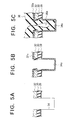
- Figures 5A to 5C are schematic sectional views of the configuration illustrating a principal part of Figs. 2B and 2C in the previously explained first method in further detail. Note that, here the parts overlapping those of Figs. 2A to 2D are indicated by the same references and thus explanations are omitted.
- the trench 34 is formed (Fig. 5A).
- an inner wall oxidized layer 34a is formed at the inner wall of the trench 34 by a thermal oxidation process.
- the thickness of the inner wall oxidized layer 34a is not particularly limited, but for example is about 10 to 30 nm.
- the inner wall oxidized layer 34a is formed for the purpose of enhancing the contact of the layer 36 to be polished filled in the trench 34 thereafter and for realizing a stable boundary surface between the insulating substance and semiconductor substrate 20, suppressing leakage via this boundary surface, and improving the insulation property. Further, this also means that the upper and lower corner portions of the trench are rounded for facilitating the filling of the layer 36 to be polished or the etching damage at the formation of the trench is eliminated.
- the intermediate layer 32 is easily oxidized (where it is made of for example polycrystalline silicon), as illustrated, at this thermal oxidation, the exposed surface of the intermediate layer 32 is also oxidized, and the surface oxidized layer 32a is formed over an area from the surface side of the intermediate layer 32 to the trench opening side wall.
- the intermediate layer 32 is made of polycrystalline silicon, it has a higher oxidation speed than the silicon substrate 20, so the surface oxidized layer 32a is formed thicker than the inner wall oxidized layer 34a.
- the lithographic technology for patterning the fine regions not only the lithographic technology for patterning the fine regions, but also the etching technology for digging the fine trench deep and a CVD technology for filling the insulating film in this fine region are important.
- the limit of miniaturization is determined by this total technology. For example, along with the miniaturization of the trench, where it is dug deep, the reaction seeds which contribute to the etching become hard to penetrate.
- the opening is closed by the coating film in the lateral direction of the insulating substance and there is a conspicuous tendency for a void to be easily formed in the trench.
- Figures 6A to 6C show a case where a borophosphosilicate glass (BPSG) film which is not thermally oxidized is used as the intermediate layer 32 so as to prevent the generation of this void 36a even in a case where the intermediate layer 32 is provided for enhancing the control of the end point of the polishing.
- BPSG borophosphosilicate glass
- a similar effect can be obtained by preliminarily nitriding the exposed surface of the intermediate layer 32 and suppressing the formation of the surface oxidized layer 32a.
- Figures 7A to 7D are schematic sectional views where the surface of the intermediate layer 32 is nitrided for preventing the generation of this void 36a.
- the intermediate layer 32 is patterned above the substrate portion on which the trench 34 should be formed in Fig. 7A, and then, as shown in Fig. 7B, the exposed surface of the intermediate layer 32 is preliminarily nitrided and the nitride layer 32b is formed.
- thermal nitridation using a lamp annealing device using for example a halogen lamp as a heat source.
- the thermal nitridation is applied for about 60 seconds under the conditions of for example 1000°C and NH 3 : 1 SLM (1/min).
- N nitrogen
- ion implantation conditions for example N ions are implanted with an energy of 3 kev and in a dosage of 1 x 10 15 /cm 2 .
- the surface oxidized layer 32a to be formed on the surface of the intermediate layer 32 can be suppressed to about 1/4 compared with the inner wall oxidized layer 34a in the trench 34. This is because, the diffusion of ion seeds is suppressed by the formation of the silicon nitride film due to the thermally nitriding or the addition of nitrogen by the ion implantation, and the progress of oxidation is prevented. As a result, it is possible to suppress the void 36a from forming in the trench 34 at the coating of the layer 36 to be polished in the not illustrated next step.
- the chemical mechanical polishing can be carried out for the layer 36 to be polished and the intermediate layer 32 until the stopper layer 30 is exposed at the surface.
- the principles of detection of terminal point and the planarization are similar to those of the case of the first method.
- the third method is a method wherein an insulation film is filled between the interconnections and the surface is planarized by the method of production of the semiconductor device.
- an interconnection layer made of a copper-containing aluminum alloy (Al-Cu) was deposited to 500 nm by a sputtering process.
- a silicon oxide film was formed by the CVD process to 100 nm.
- a tungsten (W) film was formed by the CVD process to 200 nm.
- the W, silicon oxide, and Al-Cu were successively processed by dry etching. Due to this, on the interconnection pattern 42 made of Al-Cu, a stopper layer 44 made of a silicon nitride film and an intermediate layer 46 made of a polycrystalline silicon were simultaneously formed.
- the intermediate layer 46 a material which can give selectivity can be adopted.
- the W film is used because of the fact that the temperature at the formation of the film is low and the influence on the interconnection pattern 42 is small. Accordingly, when there is no concern over the influence upon the interconnection pattern 42, it is also possible to use a polycrystalline silicon film. Also, if selectivity can be obtained, a BPSG film can be used. Note that, when polishing the W film, in addition to the KOH, hydrogen peroxide was added.
- the bias ECR/CVD process was used to deposit for example a silicon oxide film to 1000 nm as the layer 48 to be polished.
- the spaces in the interconnection pattern 42 were completely filled with the insulating substance.
- the polishing apparatus shown in Fig. 1A was used in the same way as in the first method to carry out chemical mechanical polishing of the layer 48 to be polished and the intermediate layer 46 until the stopper layer 44 was exposed at the surface.
- the principles of the detection of the end point and planarization are similar to those of the case of first method. Due to this, as shown in Fig. 8C, a planarized surface 49 of the silicon oxide film can be obtained, and the subsequent steps, for example the formation of the interconnection pattern of the second layer, can be easily carried out.
- the third method is a method of production of a semiconductor device forming a structure which effectively performs the detection of the end point of polishing and simultaneously has a stopper function of a large selectivity can be provided.
- the third method is used for trench element separation, the generation of voids in the trench accompanying the miniaturization of the trench can be prevented as much as possible. Further, it is possible to adjust the amount of projection of the layer to be polished to the remaining film thickness of the stopper layer having a slow polishing rate and make the finished shape of the element separation structure uniform.
Description
- The present invention relates to a method of producing a semiconductor device, more particularly relates to an end point control for polishing for chemical mechanical polishing for planarizing a step difference of a surface of a semiconductor substrate.
- Methods of planarizing step differences by chemical mechanical polishing have come into general use in recent years.
- On the other hand, various methods have been attempted as the method for controlling the end point of the polishing, but in actuality there has been no decisive method found from the viewpoint of precision.
- The methods for controlling the end point of polishing which have been experimented with heretofore can be roughly classified into methods not detecting the end point and methods detecting the same.
- As a method for not detecting the end point, most simply, there is known a method in which the conditions are found in advance for the relationship between the time and amount of polishing and the amount of polishing is controlled by the time based on these conditions. The polishing cloth used for the chemical mechanical polishing, however, changes in its surface state due to wear. When the same polishing cloth is used, therefore, the polishing rate fluctuates. Accordingly, when the method of controlling the amount of polishing by only the time of polishing is used in a process in which strict end point control is required such as for example trench element separation, a reduction in the manufacturing yield can not be avoided.
- So as to strictly control the end point, it is required to improve the precision of the end point detection or, even if the end point is not to be detected, to devise some measure for controlling the amount of polishing well.
- As methods for detecting the end point, there are mainly the method of monitoring the rotational torque of the polishing machine and the method of monitoring the thickness of the remaining film in parallel to the polishing.
- The method of monitoring the rotational torque of the polishing machine generally involves monitoring the rotational torque by an electrical signal such as a current as shown in Fig. 1A. Numeral 2 denotes a wafer, 4 a carrier, 6 a lathe, 8 a motor, 10 a polishing cloth, and 12 an ammeter. Detailed description of the structure will be given later. This monitoring use electrical signal does not change much at all during the time when the same film is being polished. For this reason, in order to detect the end point by this method, it is necessary to provide end point detection films having different polishing rates and to read the change of the electrical signal at the boundaries of the same.
- On the other hand, in the method of monitoring the thickness of the remaining film in parallel to the polishing, since it is possible to control the thickness of the remaining film, there also exists an advantage that it is not necessary to provide another film under the polished film. Accordingly, this method is an effective method particularly also in the case of planarizing a single layer film. More specifically, as shown in Fig. 1B, the thickness of the remaining film is optically measured by a laser
film thickness meter 14. To detect the end point of polishing by such point measurement, however, there is the prerequisite that the variation in the surface be suppressed to a certain extent. For this reason, when considering the variation of a semiconductor substrate and the polishing per se, a precision sufficient for practical use has not yet been obtained. - Next, in the method of not detecting the end point, to improve the finishing precision of the polishing, several methods using a film having a slow polishing rate as a stopper for the film to be polished have been tried. For example, these are disclosed in Japanese Unexamined Patent Publication (Kokai) Nos. 60-39835, 3-11091, 5-218000, and 6-45432. These methods include three cases, i.e., a case where the stopper film is provided at a projecting portion of a step difference, a case where it is provided at a recessed portion, and a case where it is provided on the entire surface. It was confirmed that a stopper film effectively acts to enhance the uniformity of polishing in all cases.
- In the above related arts, the most important factor is the selectivity of the polishing rates between the film to be polished and the end point detection film or the stopper film. This is because these films can be made to act more effectively the larger this selectivity.
- With the end point detection film and stopper film which have been experimented with in the related arts, however, the selectivity has not been sufficient enough to enable use in a process in which strict end point control is required.
- Giving a specific example, as the general film to be polished, a silicon oxide film formed by a CVD process is used, and as the end point detection film and stopper film in this case, a film having a slower polishing speed than the silicon oxide, for example, a silicon nitride film, is used. The selectivity at this time, that is, the ratio of the polishing rate of the silicon oxide film with respect to that of the silicon nitride film, was about 3 to 5 times.
- To further improve the selectivity, a film having a further slower polishing rate, that is, a hard film, is necessary. For this reason, films of ceramics such as boronitride films, films of diamond formed by the CVD process, and other films have been investigated, but these film-forming technologies, including also the hardware itself, still cannot be said to have been practically perfected.
- The method of production of a semiconductor device according to the present invention includes the steps of forming an intermediate layer of polycrystalline silicon by laminating materials constituting a protective layer for protecting the surface of a semiconductor substrate, a stopper layer, and the intermediate layer on the semiconductor substrate in that order and providing an opening in the intermediate layer above an element separation region of the semiconductor substrate by patterning the intermediate layer;
- nitriding the exposed surface of the formed intermediate layer and then etching the materials of the stopper layer and protective layer to extend the opening of the intermediate layer to the semiconductor substrate;
- forming a trench for the separation of an element on the semiconductor substrate exposed at the surface avia the opening;
- thermally oxidizing the inner wall of the formed trench;
- forming a layer to be polished having a slower polishing speed than that of the intermediate layer and faster polishing speed than that of the stopper layer in a manner covering the intermediate layer and filling the interior of the trench; and
- performing chemical mechanical polishing over an area from the layer to be polished to the intermediate layer.
-
- Thus, there may be provided a method of producing a semiconductor device which forms a structure which effectively detects the end point of polishing and simultaneously has a stopper function with a large selectivity.
- Thus, there is provided a method of producing a semiconductor device by planarizing the semiconductor substrate by polishing and as a result providing an intermediate layer having a high polishing rate under the layer to be polished so as to effectively detect the end point of the polishing. By doing this, a large selectivity between the layer to be polished and the intermediate layer can be imparted and the precision of detection of the end point can be raised.
- Further, by forming a stopper layer having a further larger selectivity under the intermediate layer, it is possible for the stopper layer to prevent the further progress of polishing and ensure a uniform shape after polishing. More specifically, first, a stopper layer made of a material having a slow polishing speed is formed on the portion which becomes the projecting portion of the step difference on the semiconductor substrate and an intermediate layer made of a material having a slow polishing speed is formed on this stopper layer. Thereafter, the layer to be polished is formed in a manner covering the intermediate layer and filling the recessed portion of the step difference.
- So as to effectively detect the end point by utilizing this film structure, preferably the rotational torque of the polishing machine is monitored and a large fluctuation of the rotational torque is detected as the end point of the polishing. Along with the polishing from the layer to be polished to the intermediate layer, the rotational torque of the polishing machine fluctuates particularly near the boundaries of the films at which the polishing rates differ. This rotational torque may be monitored and a fluctuation of a predetermined value or more detected so as to determine the end point of the polishing.
- The present invention is particularly suitable for the case of chemical mechanical polishing. Here, the word "chemical mechanical polishing" means a method of polishing for chemically removing fine unevenness of the surface by a basic polishing agent simultaneously with mechanical polishing. This polishing method is an excellent polishing method from the viewpoint that an extremely smooth surface is obtained. In chemical mechanical polishing, however, the chemical polishing is easily carried out at the projecting portions with relatively small pattern sizes, but at projecting portions at which the pattern size is large, the polishing agent tends to insufficiently penetrate and the chemical polishing is difficult. For this reason, if there are step differences having different pattern sizes, a variation occurs in the amount of polishing. The variation of the amount of polishing becomes conspicuous particularly when polishing a layer having a slow mechanical polishing rate, that is, a hard layer, so a variation of the amount of polishing sometimes occurs at the polishing of the layer to be polished.
- Once the intermediate layer having the slow polishing rate is exposed, however, the polishing is carried out in a manner giving a smaller variation of the amount of polishing. This is because while the polishing proceeds the larger the pattern size of the projecting portions projecting from the surface, projecting portions having a small pattern size are protected by the pattern of the projecting portions having a large size at their peripheries, so the polishing becomes more difficult. Once the variation of the amount of polishing is cancelled out during the polishing of the intermediate layer and the heights of the projecting portions become uniform, the polishing is uniformly carried out. Accordingly, if the thickness of the intermediate layer is made thick to a certain extent, at the point of time when the polishing is ended, the variation of the amount of polishing due to the difference of the size of the projecting portions is cancelled out and a surface having an extremely good planarity can be obtained.
- Even if excessive polishing is carried out after this, the stopper layer having a large selectivity effectively acts so that a surface shape having a good planarity is maintained. In addition, damage at the time of polishing to the surface of the projecting portion into which the device is formed later is prevented by these stopper layer and intermediate layer.
- It is also possible to detect the end point of polishing by the interference color which changes in accordance with the thickness of the remaining film of either of the intermediate layer or layer to be polished. In the step where the polishing is advanced, a taper is formed near for example the circumferential edge of the projecting portion for the film of either of the intermediate layer or the layer to be polished, and a color change appears due to the interference based on the thickness of the remaining film. The degree of this color change may for example be watched for by the naked eye to detect the end point. Further, it is also possible to optically detect the interference color.
- When the layer to be polished is silicon oxide, preferably the intermediate layer is made of polycrystalline silicon and the stopper layer is made of silicon nitride. Due to this, the intermediate layer can have a selectivity of 10 to 15 times with respect to the silicon oxide of the layer to be polished and 30 to 75 times with respect to the silicon nitride of the stopper layer.
- This method of production of a semiconductor device can be preferably used in the formation of trench element separation. This is because, even in a case where the amount of polishing is large as in trench element separation, strict end point control can be carried out according to the present invention. In trench element separation, after this, it is necessary to remove the stopper layer, but at the removal of this stopper layer, the protective layer protects the surface of the semiconductor substrate. Accordingly, the surface of the semiconductor substrate is not etched or does not become roughened.
- In the trench element separation, for the purpose of improving the separation characteristic by making the boundary surface between the trenc and the substrate stable, the inner wall of the trench is sometimes thinly thermally oxidized before an insulating substance (layer to be polished) is buried in the trench. Where a polycrystalline silicon film etc. is used as the intermediate layer, at this thermal oxidation, the oxide film is expanded and projects out at the side wall of the polycrystalline silicon film, which narrows the opening. Then, in the next step where the interior of the fine trench is filled with the layer to be polished, the inlet thereof is closed before the interior of the trench is completely filled with the layer to be polished and so a void is sometimes formed in the internal portion.
- To prevent this, the intermediate layer used for the trench element separation is subjected to processing of the lower layer film after nitriding the exposed surface after formation of the pattern thereof.
- This is because, by preliminarily nitriding the exposed surface of the intermediate layer, oxidation of the intermediate layer at the thermal oxidation can be suppressed.
- These and other objects and features of the present invention will become clearer from the following description of the preferred embodiments given with reference to the attached drawings, in which:
- Fig. 1A and 1B are view of a chemical mechanical polishing apparatus of the related art, wherein Fig. 1A shows the chemical mechanical polishing apparatus of the related art not using an end point control procedure and able to be used also for the working of the present invention and Fig. 1B shows a chemical mechanical polishing apparatus of the related art using an end point control procedure different from that of the present invention;
- Figs. 2A to 2D are schematic sectional views showing manufacturing steps of the semiconductor device according to the first embodiment of the present invention;
- Figs. 3A and 3B are graphs views showing the transition of the current value of the motor used for polishing in the polishing step of the present invention, where Fig. 3A shows a case where there is no intermediate layer and Fig. 3B shows a case where there is an intermediate layer;
- Fig. 4A is a graph showing the relationship between the polishing rate and the type of the layer to be polished or the surface area of the projecting portion;
- Fig. 4B is a schematic sectional view of a used sample;
- Figs. 5A to 5C are schematic sectional views of the configuration illustrating the principal parts of the steps of Figs. 2B and 2C in further detail;
- Figs. 6A to 6C are schematic sectional views of the configuration showing a second embodiment of the present invention;
- Figs. 7A to 7D are schematic sectional views of the configuration showing a third embodiment of the present invention; and
- Figs. 8A to 8C are schematic sectional views showing the manufacturing steps of a semiconductor device according to a fourth embodiment of the present invention.
-
- Below, a detailed explanation will be made of the method of production of the semiconductor device of the present invention with reference to the drawings.
- Here, before explaining the actual method of production of a semiconductor device, an explanation will be made of the apparatus for chemical mechanical polishing used for working the present invention referring to Fig. 1A.
- As shown in the figure, in the polishing apparatus used in the present embodiment, a
carrier 4 on which awafer 2 is set at amotor 8 so that the surface of thewafer 2 faces alathe 6. Further, although not particularly illustrated, a polishing agent is applied onto a polishingcloth 10 on thelathe 6. The polishing is carried out while adjusting the rotational speed of thelathe 6, the rotational speed of thecarrier 4, and the polishing pressure pressing thecarrier 4 against thelathe 6. At this time, in the sense of etching the insulation film, potassium hydroxide (KOH) etc. is added into the polishing agent and a basic atmosphere is maintained. The rotational torque of themotor 8 is monitored by anammeter 12. - This polishing apparatus is merely one example. The method of mounting the wafer, the number and structure of the
carrier 4 and thelathe 6, the type of the polishingcloth 10 and the polishing agent, etc. are not particularly limited. - A first method will be described which will aid with the understanding of the invention described in the example embodiment.
- First, as shown in Fig. 2A, a 5 nm thermal oxidation film 22 made of silicon oxide for example was formed on a
semiconductor substrate 20 made of monocrystalline silicon etc. for protection of the surface. For the formation of this thermal oxidation film 22, a thermal oxidation furnace of 850° was used. - Next, as shown in the same figure, a silicon nitride film 24 of 100 nm for example was formed and a
polycrystalline silicon film 26 of 200 nm was formed on this. - Next, as shown in Fig. 2B, a patterned resist was used as a mask for three-stage etching so as to successively etch the
polycrystalline silicon film 26, the silicon nitride film 24, and the thermal oxidation film 22. Due to this, aprotective layer 28 made of the thermal oxidation film 22, astopper layer 30 made of the silicon nitride film 24, and anintermediate layer 32 made of thepolycrystalline silicon film 26 were respectively formed in order from the bottom. Thesestopper layer 30 andintermediate layer 32 have different polishing rates in the polishing step explained later. The thickness of theintermediate layer 32 was set to a value suited for the detection of the end point of polishing as will be explained later. - Next, the
semiconductor substrate 20 was etched, and, as shown in Fig. 2B, atrench 34 of for example 500 nm was formed. - Thereafter, although not illustrated, in the
trench 34, a thermal oxidation film of 10 to 30 nm made of for example silicon oxide was formed in a thermal oxidation furnace of 950°C etc. Then, as shown in Fig. 2C, for example asilicon oxide film 36 of 1000 nm was deposited as thelayer 36 to be polished by a bias ECR-CVD process, and the interior of thetrench 34 was completely filled with the insulating substance. - Next, chemical mechanical polishing was carried out by using the polishing apparatus shown in Fig. 1A previously explained. The polishing conditions at this time were as shown in the following Table 1. These polishing conditions are general polishing conditions of an insulation film. Here, as the polishing agent, fumed silica was used. To this polishing agent, as previously explained, KOH was added. Further, as the polishing cloth, a polishing cloth-compressed urethane pad (Asker-C=90) was used.
Rotational speed of lathe 50 rpm Polishing pressure 500 g/cm2 Polishing agent Fumed silica Polishing cloth Polishing cloth-compressed urethane pad - When the chemical mechanical polishing is carried out under such conditions, the
silicon oxide film 36 on thewafer 2 surface side is chemically or mechanically removed from the swelled portion on the projecting portion of the step difference caused by trench and gradually planarized. Then, when thepolycrystalline silicon film 26 of theintermediate layer 32 is exposed at the surface, the polishing is advanced toward thestopper layer 30 made of the silicon nitride 24 while removing thepolycrystalline silicon film 26 this time. - Next, an explanation will be made of the detection of the end point of the chemical mechanical polishing. During the polishing step, the current value of the
ammeter 12 is monitored. The change of this current value is shown in Fig. 3B. During the time when thesilicon oxide film 36 is polished, the current value is a relatively high level, but when the polishing shifts to thepolycrystalline silicon film 26, it is abruptly lowered. Thereafter, the current value moves at a low level for a while and then when the polishing shifts to the silicon nitride film 24, is increased to a further higher level than the first value. - The transition of this current value corresponds to the polishing rate of the film to be polished. Namely, it reflects the fact that the polishing rate of the
polycrystalline silicon film 26 is 10 to 15 times higher than that of thesilicon oxide film motor 8 is made constant, the abrasion at the polishing becomes larger in the film having a slower polishing rate and also the load (rotational torque) applied on themotor 8 is increased. - Further, the time interval during which the current value moves at a low level corresponds to the thickness of the
intermediate layer 32 made of thepolycrystalline silicon film 26. To detect the end point with a good precision, theintermediate layer 32 must be thick to a certain extent. Conversely, when theintermediate layer 32 is too thick, however, the step difference rather becomes larger and the amount of polishing is increased. Namely, it is sufficient so far as the thickness of theintermediate layer 32 be a degree that the difference of the polishing rates is sufficiently reflected in the fluctuation of the rotational torque and is preferably 0.2±0.1 µm in the first method. - In the first method, the rotational torque of the polishing machine was monitored by the current value of the
ammeter 12, and a fluctuation of the current value of a predetermined value or more was detected as the end point of the polishing. More specifically, as shown in Fig. 3B, the detection level L was set and the point when the current value becomes the detection level L or less, that is, the point of intersection of the falling line (a-b) of the current value and the detection level L, was defined as the end point of the polishing. Note that, when the polishing apparatus is stopped at the end point of the polishing, thepolycrystalline silicon film 26 sometimes remains in part. Accordingly, it is also possible to perform some more polishing for exactly a predetermined time after this and then stop the polishing apparatus. Similarly, it is also possible to detect the end point by using the rising line (c-d) of the current value. Further, it is also possible to use the magnitude of the degree of acceleration with which the current value changes so as to detect a fluctuation of the current value of a predetermined value or more. - Note that, for comparison, the change of the current value where there is no
intermediate layer 32 made of thepolycrystalline silicon film 26 is shown in Fig. 3A. The ratio of the polishing rate of thesilicon oxide film 36 with respect to the silicon nitride film 24 is about 3 to 5 and lower than the ratio with respect to thepolycrystalline silicon film 26 by one order. For this reason, as shown in Fig. 3A, the level change of the current value becomes finer. When comparing this with Fig. 3B, the effect of inserting thepolycrystalline silicon film 26 clearly appears also in the change of the current value. - Note that, it is also possible to detect the end point of the polishing by an interference color which changes in accordance with the thickness of the remaining film. During the step where the polishing is performed, a taper is formed near for example the circumferential edge of the projecting portion for either of the
silicon oxide film 36 or thepolycrystalline silicon film 26 and a color change due to interference based on the thickness of the remaining film appears. The degree of this color change may be watched by the naked eye to detect the end point. Further, it is also possible to optically detect the interference color. In general, when the interference color of thepolycrystalline silicon film 26 is used, the detection of the end point is easy. This is because, thepolycrystalline silicon film 26 has a slow polishing rate and accordingly also the degree of the color change is large. In addition, the degree of the color change of thelower stopper layer 30 is small. Therefore, it is easy to distinguish between them. - Even if the polishing is continued as it is, after the silicon nitride film 24 having the slow polishing rate is exposed at the surface, it acts as a stopper, so the polishing does not proceed much further. Due to this, the surface state of the
planarized surface 37 of thesilicon oxide film 36 can be maintained with its good planarity. - Finally, the silicon nitride film 24 exposed at the surface is removed by phosphoric acid (H3PO4) so as to complete the trench element separation. At this time, the amount of projection of the
silicon oxide film 36 filling thetrench 34 is able to be matched with the thickness of the silicon nitride film 24. This was because, the silicon nitride film 24 effectively acted as the stopper in the step of the chemical mechanical polishing described above so polishing did not advance so much after this. Due to this, the shape of the element separation structure can be made uniform. Further, using theprotective layer 28, it was possible to protect the surface of thesemiconductor substrate 20 and prevent surface roughness. - After this, the usual steps, for example, formation of transistors etc. on the surface of the
semiconductor substrate 20 and interconnection, can be performed. - Note that, in the polishing step, if there is a difference of pattern size of the projecting portions of step differences, there sometimes occurs a variation in the amount of polishing in accordance with this pattern size. The reason for this is that, in general, in the chemical mechanical polishing, while the chemical polishing is easily carried out at projecting portions having a relatively small pattern size, at recessed portions having a large pattern size, there is insufficient permeation of the polishing agent and the chemical polishing becomes difficult. If the variation of the amount of polishing is caused by how the chemical polishing is performed in this way, there should exist a tendency for the variation to become more conspicuous the longer the polishing time.
- To examine this tendency, the relationship between the pattern sizes of the projecting portions and the polishing rate was found. The results were graphed in Fig. 4A. As the samples, as shown in Fig. 4B, step differences of various pattern sizes were formed on a silicon substrate and covered by a silicon oxide film.
- As a result, as shown in Fig. 4A, in the case of silicon oxide, which is relatively hard, that is, which has a slow polishing rate (before Si exposure), it was confirmed that the polishing rate tended to become slower in the projecting portions having a larger pattern size compared with projecting portions having a small pattern size.
- However, as shown in Fig. 4A, it was also found that if the silicon, having a slow polishing rate, is exposed (after Si exposure), this relationship was reversed. It can be considered that this is because when the polishing shifts to the silicon and the polishing rate is raised, the polishing proceeds faster the larger the size of projection from the surface of the projecting portion, while projecting portions having a small size are protected by the projecting portions having a larger size at their peripheries and so are hard to polish.
- The first method positively utilizes this characteristic of the chemical mechanical polishing. Namely, even if a variation of the amount of polishing occurs during the polishing of the
silicon oxide film 36, which is relatively hard, this can be cancelled out during the period where the nextpolycrystalline silicon film 26, which is relatively soft, is polished. For this purpose, the intermediate layer made of thepolycrystalline silicon film 26 must be thick to a certain extent. In the case of this method, as described before, the preferred thickness of theintermediate layer 32 is 0.2±0.1 µm. Within this range, the polished surface after the end of the polishing had an extremely good planarity. - Next, a second method will be explained to aid with the understanding of the invention described in the example embodiment.
- The second method relates to a method of production of a semiconductor device with which complete filling of the insulating substance (film to be polished) into the trench can be ensured even in a case where a film which is easily oxidized is selected as the intermediate layer for the strict end point control.
- Figures 5A to 5C are schematic sectional views of the configuration illustrating a principal part of Figs. 2B and 2C in the previously explained first method in further detail. Note that, here the parts overlapping those of Figs. 2A to 2D are indicated by the same references and thus explanations are omitted.
- As mentioned in the first method, after the
intermediate layer 32, thestopper layer 30, and theprotective film 28 are successively processed, thetrench 34 is formed (Fig. 5A). - Thereafter, as shown in Fig. 5B, an inner wall oxidized
layer 34a is formed at the inner wall of thetrench 34 by a thermal oxidation process. When thesilicon substrate 20 is thermally oxidized, it expands in volume about twice and the width of thetrench 34 becomes a little narrower. The thickness of the inner wall oxidizedlayer 34a is not particularly limited, but for example is about 10 to 30 nm. The inner wall oxidizedlayer 34a is formed for the purpose of enhancing the contact of thelayer 36 to be polished filled in thetrench 34 thereafter and for realizing a stable boundary surface between the insulating substance andsemiconductor substrate 20, suppressing leakage via this boundary surface, and improving the insulation property. Further, this also means that the upper and lower corner portions of the trench are rounded for facilitating the filling of thelayer 36 to be polished or the etching damage at the formation of the trench is eliminated. - Where the
intermediate layer 32 is easily oxidized (where it is made of for example polycrystalline silicon), as illustrated, at this thermal oxidation, the exposed surface of theintermediate layer 32 is also oxidized, and the surface oxidizedlayer 32a is formed over an area from the surface side of theintermediate layer 32 to the trench opening side wall. Particularly where theintermediate layer 32 is made of polycrystalline silicon, it has a higher oxidation speed than thesilicon substrate 20, so the surface oxidizedlayer 32a is formed thicker than the inner wall oxidizedlayer 34a. - Note that, in general, from the viewpoint of miniaturization, in the formation of an element separation region by a trench, not only the lithographic technology for patterning the fine regions, but also the etching technology for digging the fine trench deep and a CVD technology for filling the insulating film in this fine region are important. The limit of miniaturization is determined by this total technology. For example, along with the miniaturization of the trench, where it is dug deep, the reaction seeds which contribute to the etching become hard to penetrate. In addition, where the insulating substance is filled in the fine region next, before the trench is filled with the insulating substance, the opening is closed by the coating film in the lateral direction of the insulating substance and there is a conspicuous tendency for a void to be easily formed in the trench.
- Concerning the generation of a void in this trench, as seen from Fig. 5C, when the thickness in the lateral direction of the surface oxidized
layer 32a is large, the generation of the void 36a when forming thelayer 36 to be polished is encouraged. - Figures 6A to 6C show a case where a borophosphosilicate glass (BPSG) film which is not thermally oxidized is used as the
intermediate layer 32 so as to prevent the generation of this void 36a even in a case where theintermediate layer 32 is provided for enhancing the control of the end point of the polishing. At the formation of the inner wall oxidizedlayer 34a in Fig. 6B, thisintermediate layer 32 is almost never oxidized and the opening of thetrench 34 does not become narrow, so in the next film coating step of thelayer 36 to be polished in Fig. 6C, the interior of thetrench 34 can be completely filled with thelayer 36 to be polished. - A similar effect can be obtained by preliminarily nitriding the exposed surface of the
intermediate layer 32 and suppressing the formation of the surface oxidizedlayer 32a. - Next, an example embodiment of the present invention will be explained.
- Figures 7A to 7D are schematic sectional views where the surface of the
intermediate layer 32 is nitrided for preventing the generation of this void 36a. First, theintermediate layer 32 is patterned above the substrate portion on which thetrench 34 should be formed in Fig. 7A, and then, as shown in Fig. 7B, the exposed surface of theintermediate layer 32 is preliminarily nitrided and thenitride layer 32b is formed. - As the method of the surface nitriding, there is thermal nitridation using a lamp annealing device using for example a halogen lamp as a heat source. The thermal nitridation is applied for about 60 seconds under the conditions of for example 1000°C and NH3: 1 SLM (1/min).
- Further, there also exists a method of adding nitrogen (N) by an ion implantation method. As the ion implantation conditions in this case, for example N ions are implanted with an energy of 3 kev and in a dosage of 1 x 10¹⁵/cm2.
- By this, as shown in Fig. 7D, the surface oxidized
layer 32a to be formed on the surface of theintermediate layer 32 can be suppressed to about 1/4 compared with the inner wall oxidizedlayer 34a in thetrench 34. This is because, the diffusion of ion seeds is suppressed by the formation of the silicon nitride film due to the thermally nitriding or the addition of nitrogen by the ion implantation, and the progress of oxidation is prevented. As a result, it is possible to suppress the void 36a from forming in thetrench 34 at the coating of thelayer 36 to be polished in the not illustrated next step. - After this, by using the polishing apparatus shown in Fig. 1A, in the same way as the first method, the chemical mechanical polishing can be carried out for the
layer 36 to be polished and theintermediate layer 32 until thestopper layer 30 is exposed at the surface. The principles of detection of terminal point and the planarization are similar to those of the case of the first method. - Further, a third method will be explained to aid with the understanding of the invention described in the example embodiment.
- The third method is a method wherein an insulation film is filled between the interconnections and the surface is planarized by the method of production of the semiconductor device.
- First, on the
underlying insulation film 40 made of silicon oxide, an interconnection layer made of a copper-containing aluminum alloy (Al-Cu) was deposited to 500 nm by a sputtering process. On this, for example, a silicon oxide film was formed by the CVD process to 100 nm. Further, for example, a tungsten (W) film was formed by the CVD process to 200 nm. - Next, as shown in Fig. 8A, by using the patterned resist as the mask, the W, silicon oxide, and Al-Cu were successively processed by dry etching. Due to this, on the
interconnection pattern 42 made of Al-Cu, astopper layer 44 made of a silicon nitride film and anintermediate layer 46 made of a polycrystalline silicon were simultaneously formed. Here, as theintermediate layer 46, a material which can give selectivity can be adopted. In this method the W film is used because of the fact that the temperature at the formation of the film is low and the influence on theinterconnection pattern 42 is small. Accordingly, when there is no concern over the influence upon theinterconnection pattern 42, it is also possible to use a polycrystalline silicon film. Also, if selectivity can be obtained, a BPSG film can be used. Note that, when polishing the W film, in addition to the KOH, hydrogen peroxide was added. - Thereafter, as shown in Fig. 8B, the bias ECR/CVD process was used to deposit for example a silicon oxide film to 1000 nm as the
layer 48 to be polished. The spaces in theinterconnection pattern 42 were completely filled with the insulating substance. - Next, the polishing apparatus shown in Fig. 1A was used in the same way as in the first method to carry out chemical mechanical polishing of the
layer 48 to be polished and theintermediate layer 46 until thestopper layer 44 was exposed at the surface. The principles of the detection of the end point and planarization are similar to those of the case of first method. Due to this, as shown in Fig. 8C, aplanarized surface 49 of the silicon oxide film can be obtained, and the subsequent steps, for example the formation of the interconnection pattern of the second layer, can be easily carried out. - As explained above, the third method is a method of production of a semiconductor device forming a structure which effectively performs the detection of the end point of polishing and simultaneously has a stopper function of a large selectivity can be provided.
- Also, it is possible to cancel out the variation in polishing due to the pattern size at the chemical mechanical polishing in hte polishing step and finally obtain an extremely good planarity. In addition, there also exists an effect of prevention of damage at the polishing.
- Further, where the third method is used for trench element separation, the generation of voids in the trench accompanying the miniaturization of the trench can be prevented as much as possible. Further, it is possible to adjust the amount of projection of the layer to be polished to the remaining film thickness of the stopper layer having a slow polishing rate and make the finished shape of the element separation structure uniform.
Claims (5)
- A method of producing a semiconductor including the steps of:forming an intermediate layer (32) of polycrystalline silicon by laminating materials constituting a protective layer (28) for protecting the surface of a semiconductor substrate (20), a stopper layer (30), and the intermediate layer (32) on the semiconductor substrate (20) in that order and providing an opening in the intermediate layer above an element separation region of the semiconductor substrate (20) by patterning the intermediate layer (32);nitriding (32b) the exposed surface of the formed intermediate layer (32) and then etching the materials of the stopper layer (30) and protective layer (28) to extend the opening of the intermediate layer (32) to the semiconductor substrate (20) ;forming a trench (34) for the separation of an element on the semiconductor substrate (20) exposed at the surface via the opening;thermally oxidizing the inner wall of the formed trench;forming a layer (36) to be polished having a slower polishing speed than that of the intermediate layer (32) and faster polishing speed than that of the stopper layer (30) in a manner covering the intermediate layer (32) and filling the interior of the trench (34); andperforming chemical mechanical polishing over an area from the layer to be polished (36) to the intermediate layer (32).
- A method of producing a semiconductor device as set forth in claim 1, wherein the polishing comprises chemical mechanical polishing.
- A method of producing a semiconductor device as set forth in claim 1 or 2, wherein in the step of performing the polishing, a rotational torque of a polishing machine is monitored and a fluctuation of the rotational torque of a predetermined value or more is detected as the end point of the polishing.
- A method of producing a semiconductor device as set forth in claim 1, 2 or 3, wherein in the step of performing the polishing, the end point of the polishing is detected by an interference color changing in accordance with the thickness of the remaining film of one of the intermediate layer (32) or the layer (36) to be polished.
- A method of producing a semiconductor device as set forth in any one of the preceding claims, wherein the layer (36) to be polished is made of silicon oxide, and the stopper layer (30) is made of silicon nitride.
Applications Claiming Priority (6)
| Application Number | Priority Date | Filing Date | Title |
|---|---|---|---|
| JP116069/95 | 1995-05-15 | ||
| JP11606995 | 1995-05-15 | ||
| JP11606995 | 1995-05-15 | ||
| JP30440895A JP3438446B2 (en) | 1995-05-15 | 1995-11-22 | Method for manufacturing semiconductor device |
| JP30440895 | 1995-11-22 | ||
| JP304408/95 | 1995-11-22 |
Publications (3)
| Publication Number | Publication Date |
|---|---|
| EP0743674A2 EP0743674A2 (en) | 1996-11-20 |
| EP0743674A3 EP0743674A3 (en) | 1998-02-25 |
| EP0743674B1 true EP0743674B1 (en) | 2000-09-13 |
Family
ID=26454448
Family Applications (1)
| Application Number | Title | Priority Date | Filing Date |
|---|---|---|---|
| EP96303170A Expired - Lifetime EP0743674B1 (en) | 1995-05-15 | 1996-05-07 | Method of etching back layer on substrate |
Country Status (5)
| Country | Link |
|---|---|
| US (1) | US5736462A (en) |
| EP (1) | EP0743674B1 (en) |
| JP (1) | JP3438446B2 (en) |
| KR (1) | KR960042997A (en) |
| DE (1) | DE69610252T2 (en) |
Families Citing this family (38)
| Publication number | Priority date | Publication date | Assignee | Title |
|---|---|---|---|---|
| US6225230B1 (en) * | 1996-05-28 | 2001-05-01 | Kabushiki Kaisha Toshiba | Method of manufacturing semiconductor device |
| JP4195734B2 (en) * | 1996-06-10 | 2008-12-10 | テキサス インスツルメンツ インコーポレイテツド | Integrated circuit trench isolation fabrication method |
| JP3688816B2 (en) * | 1996-07-16 | 2005-08-31 | 株式会社東芝 | Manufacturing method of semiconductor device |
| JP3571887B2 (en) * | 1996-10-18 | 2004-09-29 | キヤノン株式会社 | Active matrix substrate and liquid crystal device |
| JPH10217149A (en) * | 1997-02-05 | 1998-08-18 | Ebara Corp | Cloth exfoliating jig for turntable |
| US6117777A (en) * | 1997-07-30 | 2000-09-12 | Chartered Semiconductor Manufacturing Co. | Chemical mechanical polish (CMP) endpoint detection by colorimetry |
| DE19733391C2 (en) * | 1997-08-01 | 2001-08-16 | Siemens Ag | Structuring process |
| US5943590A (en) * | 1997-09-15 | 1999-08-24 | Winbond Electronics Corp. | Method for improving the planarity of shallow trench isolation |
| US6143625A (en) * | 1997-11-19 | 2000-11-07 | Texas Instruments Incorporated | Protective liner for isolation trench side walls and method |
| JP3519589B2 (en) * | 1997-12-24 | 2004-04-19 | 株式会社ルネサステクノロジ | Manufacturing method of semiconductor integrated circuit |
| US6228769B1 (en) * | 1998-05-06 | 2001-05-08 | International Business Machines Corporation | Endpoint detection by chemical reaction and photoionization |
| US6066564A (en) * | 1998-05-06 | 2000-05-23 | International Business Machines Corporation | Indirect endpoint detection by chemical reaction |
| US6071818A (en) | 1998-06-30 | 2000-06-06 | Lsi Logic Corporation | Endpoint detection method and apparatus which utilize an endpoint polishing layer of catalyst material |
| US6077783A (en) * | 1998-06-30 | 2000-06-20 | Lsi Logic Corporation | Method and apparatus for detecting a polishing endpoint based upon heat conducted through a semiconductor wafer |
| US6268224B1 (en) | 1998-06-30 | 2001-07-31 | Lsi Logic Corporation | Method and apparatus for detecting an ion-implanted polishing endpoint layer within a semiconductor wafer |
| US6241847B1 (en) | 1998-06-30 | 2001-06-05 | Lsi Logic Corporation | Method and apparatus for detecting a polishing endpoint based upon infrared signals |
| US6326309B2 (en) * | 1998-06-30 | 2001-12-04 | Fujitsu Limited | Semiconductor device manufacturing method |
| US6074517A (en) * | 1998-07-08 | 2000-06-13 | Lsi Logic Corporation | Method and apparatus for detecting an endpoint polishing layer by transmitting infrared light signals through a semiconductor wafer |
| US6285035B1 (en) | 1998-07-08 | 2001-09-04 | Lsi Logic Corporation | Apparatus for detecting an endpoint polishing layer of a semiconductor wafer having a wafer carrier with independent concentric sub-carriers and associated method |
| US6080670A (en) * | 1998-08-10 | 2000-06-27 | Lsi Logic Corporation | Method of detecting a polishing endpoint layer of a semiconductor wafer which includes a non-reactive reporting specie |
| US5972787A (en) * | 1998-08-18 | 1999-10-26 | International Business Machines Corp. | CMP process using indicator areas to determine endpoint |
| US6201253B1 (en) | 1998-10-22 | 2001-03-13 | Lsi Logic Corporation | Method and apparatus for detecting a planarized outer layer of a semiconductor wafer with a confocal optical system |
| US6121147A (en) * | 1998-12-11 | 2000-09-19 | Lsi Logic Corporation | Apparatus and method of detecting a polishing endpoint layer of a semiconductor wafer which includes a metallic reporting substance |
| US6117779A (en) * | 1998-12-15 | 2000-09-12 | Lsi Logic Corporation | Endpoint detection method and apparatus which utilize a chelating agent to detect a polishing endpoint |
| US6316276B1 (en) | 1998-12-17 | 2001-11-13 | Lsi Lgoic Corporation | Apparatus and method of planarizing a semiconductor wafer that includes a first reflective substance and a second reflective substance |
| DE19946493C2 (en) * | 1999-09-28 | 2002-05-16 | Infineon Technologies Ag | Process for removing layers |
| US7751609B1 (en) | 2000-04-20 | 2010-07-06 | Lsi Logic Corporation | Determination of film thickness during chemical mechanical polishing |
| US6645825B1 (en) | 2000-07-12 | 2003-11-11 | Taiwan Semiconductor Manufacturing Company | Planarization of shallow trench isolation (STI) |
| TWI228538B (en) * | 2000-10-23 | 2005-03-01 | Kao Corp | Polishing composition |
| US6593238B1 (en) * | 2000-11-27 | 2003-07-15 | Motorola, Inc. | Method for determining an endpoint and semiconductor wafer |
| US6664190B2 (en) | 2001-09-14 | 2003-12-16 | Chartered Semiconductor Manufacturing Ltd. | Pre STI-CMP planarization scheme |
| US6741913B2 (en) * | 2001-12-11 | 2004-05-25 | International Business Machines Corporation | Technique for noise reduction in a torque-based chemical-mechanical polishing endpoint detection system |
| JP2003318140A (en) * | 2002-04-26 | 2003-11-07 | Applied Materials Inc | Polishing method and device thereof |
| US7102206B2 (en) | 2003-01-20 | 2006-09-05 | Matsushita Electric Industrial Co., Ltd. | Semiconductor substrate, method for fabricating the same, and method for fabricating semiconductor device |
| US20050197048A1 (en) * | 2004-03-04 | 2005-09-08 | Leping Li | Method for manufacturing a workpiece and torque transducer module |
| JP2006245036A (en) * | 2005-02-28 | 2006-09-14 | Seiko Epson Corp | Forming method of element isolation layer, manufacturing method of electronic device, and cmp apparatus |
| US8497210B2 (en) | 2010-10-04 | 2013-07-30 | International Business Machines Corporation | Shallow trench isolation chemical mechanical planarization |
| US9825128B2 (en) | 2015-10-20 | 2017-11-21 | Maxpower Semiconductor, Inc. | Vertical power transistor with thin bottom emitter layer and dopants implanted in trenches in shield area and termination rings |
Family Cites Families (17)
| Publication number | Priority date | Publication date | Assignee | Title |
|---|---|---|---|---|
| US3911562A (en) * | 1974-01-14 | 1975-10-14 | Signetics Corp | Method of chemical polishing of planar silicon structures having filled grooves therein |
| JPS6039835A (en) * | 1983-08-12 | 1985-03-01 | Hitachi Ltd | Flattening of surface of substrate |
| US4666556A (en) * | 1986-05-12 | 1987-05-19 | International Business Machines Corporation | Trench sidewall isolation by polysilicon oxidation |
| JPH0311091A (en) * | 1989-06-06 | 1991-01-18 | Toray Ind Inc | Novel platinum (ii) complex and remedy for malignant tumor |
| US5096550A (en) * | 1990-10-15 | 1992-03-17 | The United States Of America As Represented By The United States Department Of Energy | Method and apparatus for spatially uniform electropolishing and electrolytic etching |
| US5290396A (en) * | 1991-06-06 | 1994-03-01 | Lsi Logic Corporation | Trench planarization techniques |
| JP3208575B2 (en) * | 1991-08-16 | 2001-09-17 | ソニー株式会社 | Semiconductor device manufacturing method |
| US5376222A (en) * | 1991-09-04 | 1994-12-27 | Fujitsu Limited | Polishing method for polycrystalline silicon |
| US5246884A (en) * | 1991-10-30 | 1993-09-21 | International Business Machines Corporation | Cvd diamond or diamond-like carbon for chemical-mechanical polish etch stop |
| JP2946920B2 (en) * | 1992-03-09 | 1999-09-13 | 日本電気株式会社 | Method for manufacturing semiconductor device |
| US5229316A (en) * | 1992-04-16 | 1993-07-20 | Micron Technology, Inc. | Semiconductor processing method for forming substrate isolation trenches |
| GB2275129B (en) * | 1992-05-26 | 1997-01-08 | Toshiba Kk | Method for planarizing a layer on a semiconductor wafer |
| JP3190742B2 (en) * | 1992-10-12 | 2001-07-23 | 株式会社東芝 | Polishing method |
| JPH07111962B2 (en) * | 1992-11-27 | 1995-11-29 | 日本電気株式会社 | Selective flattening polishing method |
| US5356513A (en) * | 1993-04-22 | 1994-10-18 | International Business Machines Corporation | Polishstop planarization method and structure |
| JPH07235537A (en) * | 1994-02-23 | 1995-09-05 | Mitsubishi Electric Corp | Semiconductor device with flattened surface and manufacture thereof |
| JPH07249626A (en) * | 1994-03-10 | 1995-09-26 | Toshiba Corp | Manufacture of semiconductor device |
-
1995
- 1995-11-22 JP JP30440895A patent/JP3438446B2/en not_active Expired - Fee Related
-
1996
- 1996-04-26 US US08/638,205 patent/US5736462A/en not_active Expired - Fee Related
- 1996-05-04 KR KR19960014530A patent/KR960042997A/ko not_active Application Discontinuation
- 1996-05-07 EP EP96303170A patent/EP0743674B1/en not_active Expired - Lifetime
- 1996-05-07 DE DE69610252T patent/DE69610252T2/en not_active Expired - Fee Related
Also Published As
| Publication number | Publication date |
|---|---|
| DE69610252T2 (en) | 2001-04-05 |
| US5736462A (en) | 1998-04-07 |
| DE69610252D1 (en) | 2000-10-19 |
| KR960042997A (en) | 1996-12-21 |
| EP0743674A3 (en) | 1998-02-25 |
| JPH0936073A (en) | 1997-02-07 |
| JP3438446B2 (en) | 2003-08-18 |
| EP0743674A2 (en) | 1996-11-20 |
Similar Documents
| Publication | Publication Date | Title |
|---|---|---|
| EP0743674B1 (en) | Method of etching back layer on substrate | |
| US6709951B2 (en) | Oxynitride shallow trench isolation and method of formation | |
| US5316965A (en) | Method of decreasing the field oxide etch rate in isolation technology | |
| US6080636A (en) | Photolitography alignment mark manufacuturing process in tungsten CMP metallization | |
| US6348395B1 (en) | Diamond as a polish-stop layer for chemical-mechanical planarization in a damascene process flow | |
| JP4593521B2 (en) | Trench element isolation method for integrated circuit device using high selectivity CMP | |
| US6319796B1 (en) | Manufacture of an integrated circuit isolation structure | |
| US6015757A (en) | Method of oxide etching with high selectivity to silicon nitride by using polysilicon layer | |
| US5874345A (en) | Method for planarizing TEOS SiO2 filled shallow isolation trenches | |
| Stavreva et al. | Chemical-mechanical polishing of copper for interconnect formation | |
| US6066550A (en) | Method of improving selectivity between silicon nitride and silicon oxide | |
| US7410873B2 (en) | Method of manufacturing a semiconductor device | |
| US5930585A (en) | Collar etch method to improve polysilicon strap integrity in DRAM chips | |
| Cooperman et al. | Optimization of a shallow trench isolation process for improved planarization | |
| US6653202B1 (en) | Method of shallow trench isolation (STI) formation using amorphous carbon | |
| JPS6039835A (en) | Flattening of surface of substrate | |
| US6863595B1 (en) | Methods for polishing a semiconductor topography | |
| JP3311486B2 (en) | Integrated circuit planarization method | |
| JP3116879B2 (en) | Method for manufacturing semiconductor device | |
| EP0939437A2 (en) | Planarization of wiring layers | |
| KR0177396B1 (en) | Flattening method of semiconductor device | |
| US6613648B1 (en) | Shallow trench isolation using TEOS cap and polysilicon pullback | |
| JP3245076B2 (en) | How to flatten shallow isolation trenches | |
| JPH11260772A (en) | Surface flattening method | |
| GB2360630A (en) | Semiconductor device having device section and alignment mark section with isolation regions |
Legal Events
| Date | Code | Title | Description |
|---|---|---|---|
| PUAI | Public reference made under article 153(3) epc to a published international application that has entered the european phase |
Free format text: ORIGINAL CODE: 0009012 |
|
| AK | Designated contracting states |
Kind code of ref document: A2 Designated state(s): DE FR GB |
|
| PUAL | Search report despatched |
Free format text: ORIGINAL CODE: 0009013 |
|
| AK | Designated contracting states |
Kind code of ref document: A3 Designated state(s): DE FR GB |
|
| 17P | Request for examination filed |
Effective date: 19980729 |
|
| 17Q | First examination report despatched |
Effective date: 19980929 |
|
| GRAG | Despatch of communication of intention to grant |
Free format text: ORIGINAL CODE: EPIDOS AGRA |
|
| GRAG | Despatch of communication of intention to grant |
Free format text: ORIGINAL CODE: EPIDOS AGRA |
|
| GRAH | Despatch of communication of intention to grant a patent |
Free format text: ORIGINAL CODE: EPIDOS IGRA |
|
| GRAH | Despatch of communication of intention to grant a patent |
Free format text: ORIGINAL CODE: EPIDOS IGRA |
|
| GRAA | (expected) grant |
Free format text: ORIGINAL CODE: 0009210 |
|
| AK | Designated contracting states |
Kind code of ref document: B1 Designated state(s): DE FR GB |
|
| REF | Corresponds to: |
Ref document number: 69610252 Country of ref document: DE Date of ref document: 20001019 |
|
| ET | Fr: translation filed | ||
| PLBE | No opposition filed within time limit |
Free format text: ORIGINAL CODE: 0009261 |
|
| STAA | Information on the status of an ep patent application or granted ep patent |
Free format text: STATUS: NO OPPOSITION FILED WITHIN TIME LIMIT |
|
| 26N | No opposition filed | ||
| REG | Reference to a national code |
Ref country code: GB Ref legal event code: IF02 |
|
| PGFP | Annual fee paid to national office [announced via postgrant information from national office to epo] |
Ref country code: GB Payment date: 20030507 Year of fee payment: 8 |
|
| PGFP | Annual fee paid to national office [announced via postgrant information from national office to epo] |
Ref country code: FR Payment date: 20030508 Year of fee payment: 8 |
|
| PGFP | Annual fee paid to national office [announced via postgrant information from national office to epo] |
Ref country code: DE Payment date: 20030515 Year of fee payment: 8 |
|
| PG25 | Lapsed in a contracting state [announced via postgrant information from national office to epo] |
Ref country code: GB Free format text: LAPSE BECAUSE OF NON-PAYMENT OF DUE FEES Effective date: 20040507 |
|
| PG25 | Lapsed in a contracting state [announced via postgrant information from national office to epo] |
Ref country code: DE Free format text: LAPSE BECAUSE OF NON-PAYMENT OF DUE FEES Effective date: 20041201 |
|
| GBPC | Gb: european patent ceased through non-payment of renewal fee |
Effective date: 20040507 |
|
| PG25 | Lapsed in a contracting state [announced via postgrant information from national office to epo] |
Ref country code: FR Free format text: LAPSE BECAUSE OF NON-PAYMENT OF DUE FEES Effective date: 20050131 |
|
| REG | Reference to a national code |
Ref country code: FR Ref legal event code: ST |