EP0757428B1 - Flyback converter - Google Patents
Flyback converter Download PDFInfo
- Publication number
- EP0757428B1 EP0757428B1 EP95410075A EP95410075A EP0757428B1 EP 0757428 B1 EP0757428 B1 EP 0757428B1 EP 95410075 A EP95410075 A EP 95410075A EP 95410075 A EP95410075 A EP 95410075A EP 0757428 B1 EP0757428 B1 EP 0757428B1
- Authority
- EP
- European Patent Office
- Prior art keywords
- switching device
- diode
- voltage
- circuit
- primary
- Prior art date
- Legal status (The legal status is an assumption and is not a legal conclusion. Google has not performed a legal analysis and makes no representation as to the accuracy of the status listed.)
- Expired - Lifetime
Links
Images


Classifications
-
- H—ELECTRICITY
- H01—ELECTRIC ELEMENTS
- H01F—MAGNETS; INDUCTANCES; TRANSFORMERS; SELECTION OF MATERIALS FOR THEIR MAGNETIC PROPERTIES
- H01F38/00—Adaptations of transformers or inductances for specific applications or functions
- H01F38/42—Flyback transformers
-
- H—ELECTRICITY
- H02—GENERATION; CONVERSION OR DISTRIBUTION OF ELECTRIC POWER
- H02M—APPARATUS FOR CONVERSION BETWEEN AC AND AC, BETWEEN AC AND DC, OR BETWEEN DC AND DC, AND FOR USE WITH MAINS OR SIMILAR POWER SUPPLY SYSTEMS; CONVERSION OF DC OR AC INPUT POWER INTO SURGE OUTPUT POWER; CONTROL OR REGULATION THEREOF
- H02M3/00—Conversion of dc power input into dc power output
- H02M3/22—Conversion of dc power input into dc power output with intermediate conversion into ac
- H02M3/24—Conversion of dc power input into dc power output with intermediate conversion into ac by static converters
- H02M3/28—Conversion of dc power input into dc power output with intermediate conversion into ac by static converters using discharge tubes with control electrode or semiconductor devices with control electrode to produce the intermediate ac
- H02M3/325—Conversion of dc power input into dc power output with intermediate conversion into ac by static converters using discharge tubes with control electrode or semiconductor devices with control electrode to produce the intermediate ac using devices of a triode or a transistor type requiring continuous application of a control signal
- H02M3/335—Conversion of dc power input into dc power output with intermediate conversion into ac by static converters using discharge tubes with control electrode or semiconductor devices with control electrode to produce the intermediate ac using devices of a triode or a transistor type requiring continuous application of a control signal using semiconductor devices only
- H02M3/33507—Conversion of dc power input into dc power output with intermediate conversion into ac by static converters using discharge tubes with control electrode or semiconductor devices with control electrode to produce the intermediate ac using devices of a triode or a transistor type requiring continuous application of a control signal using semiconductor devices only with automatic control of the output voltage or current, e.g. flyback converters
Definitions
- the present invention relates to a switched mode power supply in the form of a flyback converter.
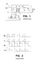
- Flyback converters are well known in the art and Figure 1 of the accompanying drawings shows the main components of a basic flyback converter 10.
- the converter 10 comprises an input circuit 11 coupled to an output circuit 12 through an energy-storing transformer 13 that has primary and secondary windings 14 and 15 respectively.
- the input circuit 11 comprises a switching device 16 (shown as a MOSFET in Figure 1) connected in series with the transformer primary winding 14, and a control block 17 for controlling the cyclic turning on and off of the switching device 16.
- the output circuit 12 comprises a diode 18 connected in series with the transformer secondary winding 15, and a reservoir capacitor 19 connected in parallel with the series combination of the secondary winding 15 and diode 18 and across which the converter output is produced.
- a load 20 is connected across the converter output.
- the MOSFET switching device 16 is cyclically turned on by a waveform V gs applied to its gate, the MOSFET being oil (see waveform V ds , the voltage across the MOSFET) when the gate voltage waveform V gs is high.
- V ds the voltage across the MOSFET
- current I d builds at a steady rate through the transformer primary winding 14 and energy is stored in the flux in the transformer core.
- the MOSFET turns off and the magnetic flux in the transformer progressively collapses driving a current I rect through the secondary winding 15 and diode 18 towards the load 20.
- the flux in the transformer core does not fall to zero prior to the MOSFET turning on again to restart the cycle of operation; as a result, the current I rect also does not reach zero before the cycle restarts.
- This mode of operation is known as the continuous mode. It is also possible for the converter to operate in a discontinous mode in which the transformer is fully discharged before the MOSFET is turned on again in which case the current I rect will fall to zero earlier than the turn on of the MOSFET.
- the output voltage of the converter 10 is regulated by the feedback of the output voltage to the control block 17.
- the output circuit will be electrically isolated from the input circuit so that the feedback path will normally include an isolating element (this is signified in Figure 1 by using a dashed oval to depict the feedback loop as only indirectly connected to the output circuit).
- the switching frequency of the switching device 16 is fixed and the control block 17 controls the duty cycle of the switching device (i.e. effects a pulse width modulation control) to keep the output voltage constant.
- the need to comply with a variety of safety regulations means that the leakage inductance can be up to one fifth of the main inductance.
- the efficiency of the power supply in this case is thus immediately limited to 80% due just to this phenomenon; the practical efficiency will then be around 60% for low line operations.
- At least part of the energy stored in the primary leakage inductance is transferred to the output circuit and converted into a dc component of the converter output so that it is dissipated as useful energy in the load.
- a flyback converter in which a first tuning capacitance is provided in the input circuit either physically connected in parallel with the transformer primary winding or in a position that in terms of a.c. functional effect is equivalent to such a parallel connection, and in which a second tuning capacitance is provided in the output circuit either physically connected in parallel with the transformer secondary winding or in a position that in terms of a.c. functional effect is equivalent to such a parallel connection, these tuning capacitances having values such that:
- the first tuning capacitance may be provided at least in part by a capacitor connected across the primary winding; however, where the switching device is a MOSFET, then the source-drain capacitance of the MOSFET will provide, at least in part, the first tuning capacitance.
- the second tuning capacitance this can be provided at least in part by a capacitor connected across either the secondary winding or the diode; furthermore, where the converter has multiple output circuits, the second tuning capacitance can be divided between the output circuits.
- the non-linear device will generally be constituted by the output-circuit diode. However, it is also possible to use other arrangements such as a MOSFET connected in series with the diode, and means for switching the MOSFET on and off in synchronism with said ringing.
- the switching-device control means preferably comprises sensing means for sensing the voltage across the switching device when the latter is off, determining means for determining a minimum of the voltage sensed by the sensing means, and turn-on means for turning on the switching device at a said minimum of the voltage thereacross as determined by the determining means.
- the sensing means comprises a sensing winding wound jointly with the transformer primary and secondary windings
- the determining means comprises integration means for integrating the voltage sensed by the sensing winding, and means for detecting a zero crossing of the voltage integrated by the integration means, this zero crossing being indicative of the said minimum of the voltage across the switching device.
- control means preferably further comprises time-out means for initiating turn on of the switching device a predetermined time after when the switching device was last on unless the latter is earlier turned on again by the turn-on means.
- the first part of the following aims at building an understanding of the invention by a consideration of certain contributory effects.
- the present invention can be characterised as first making the energy stored in the primary leakage inductanc available for use in the output circuit and then transferring this energy to the load as a dc component of the converter output.
- Figure 3 shows a tuned tank coil circuit that permits such a transfer between inductors 22 and 23 that are coupled by a coupling factor k.
- an ac source 24 with impedance R s drives a current I 1 into a tuned circuit comprising the inductor 22 and a capacitor 25.
- the inductor 23 is connected to a load R load .
- the foregoing can be applied to a flyback converter by considering the primary leakage inductance and the secondary inductance to be the inductors 22 and 23 respectively that have limited coupling k, and then providing a tuning capacitor across the transformer primary leakage inductance to give a Q value appropriate to the coupling factor k.
- the primary leakage inductance and the secondary inductance to be the inductors 22 and 23 respectively that have limited coupling k
- a tuning capacitor across the transformer primary leakage inductance to give a Q value appropriate to the coupling factor k.
- the tuning capacitor cannot simply be coupled across the primary leakage inductance but necessarily will also parallel the main primary inductance (this is dealt with further hereinafter).
- Figure 4 shows the Figure 1 flyback converter 10 to which a tuning capacitor 30 has been added in parallel with the primary winding 14 to set up the ringing conditions described above.
- Figure 5 illustrates for the Figure 4 converter the same voltage and current timeplots as shown in Figure 2 in respect of the Figure 1 converter.
- the presence of the primary tuning capacitor creates a substantial ringing in the drain voltage V ds of the MOSFET 16 and in the current I rect through the output-circuit diode 18.
- the tuning capacitor 30 is represented by a capacitance of value C.
- the transformer is represented, as viewed from the primary side, as a leakage inductance of value "1" and a main inductance of value "L", these inductances being combinations of the primary and secondary leakage and main inductances respectively; the resistive and magnetising force elements required to more fully represent a real transformer have been omitted for simplicity of explantion.
- the transformer 13 has a turns ratio "n" of unity thereby avoiding the need to introduce a factor of n 2 when transferring impedances from one side of the transformer to the other; it will be readily apparent to persons skilled in the art that the generality of the following explanations will apply equally to cases where the turns ratio n is other than unity and the resistive and magnetising force elements of the transformer are taken into account.
- the diode 18 Following turn off of the MOSFET 16, the diode 18 starts to conduct. In ac terms, the conduction of diode 18 effectively shorts the secondary winding 15 so that, referring to Figure 6, the inductance L plays no part in determining the response of the equivalent circuit.
- the capacitor 30 and transformer 13 form a parallel resonant circuit made up of the capacitance C and leakage inductance 1. It is this resonant circuit which determines the frequency F R of the ringing caused upon turn off of MOSFET 16 by the energy in the leakage inductance.
- Figure 7 shows the current/voltage phase response characteristic 31 of the Figure 4 converter as viewed at the transformer primary for the case when the diode is conducting (ON); as would be expected, phase reversal occurs at the ringing frequency F R .
- the expression given for F R in Figure 7 is, of course, only approximate.
- the inductance L plays a full role in determining the response of the Figure 6 equivalent circuit.
- the capacitance C and inductances l and L now form a different resonant circuit with a resonant frequency F O lower than the ringing frequency F R .
- This resonance at frequency F O generally does not effect the operation of the Figure 4 converter provided, of course, that the switching frequency of the MOSFET is sufficiently spaced from the frequency F O .
- Figure 7 shows the phase response characteristic 32 of the Figure 4 converter for the case where the diode 18 is non-conducting (OFF); as with F R , the expression given for F O in Figure 7 is only approximate.
- the present invention provides for the generation, as part of the secondary current, of a component at the same frequency as, but in anti-phase to, the ringing frequency component; these components are then mixed in a non-linear device (which will generally be the rectifier diode itself) to give a dc component useful for powering the load.
- a non-linear device which will generally be the rectifier diode itself
- Figure 9 depicts the transformer equivalent circuit produced by the addition of capacitor 35, this equivalent circuit corresponding to that of Figure 6 but with addition of a capacitance C' corresponding to the value of capacitor 35 (it being recalled that the transformer is, for simplicity, assumed to have a turns ratio n of unity).
- the effect of the second tuning capacitor may be understood in qualitive terms by reference to the Figure 9 equivalent circuit and to the phase response characteristics shown in Figure 10 for the Figure 8 converter for the diode conducting (ON) and diode non-conducting (OFF) conditions.
- the frequency characteristics of the Figure 8 converter are substantially the same as for the Figure 4 converter because the second tuning capacitor 35 is effectively shorted; thus, there exists a parallel resonant circuit involving the capacitance C (the first tuning capacitor 30) and the leakage inductance l, the resonant frequency of this resonant circuit being F R .
- Phase reversal occurs at the frequency F R as can be seen from the phase response characteristic 36 shown in Figure 10 for the diode on condition.
- the second tuning capacitor C' has a significant effect on the frequency characteristics of the Figure 8 converter as compared to the Figure 4 converter.
- a phase reversal occurs at this resonance frequency F O as can be seen from the phase response characteristic 37 shown in Figure 10 for the diode off condition (again, note that the formula given for F O in Figure 10 is highly approximate as can be seen by the omission of the leakage inductance l).
- phase responses exhibited in the diode-off and diode-on conditions are in anti-phase. It can now be seen that if during the ringing that takes place following turn off of MOSFET 16, a sufficiently large downward swing occurs to take the diode out of conduction, the phase of the current is immediately reversed as operation switches from the diode-on to the diode-off condition and this will drive the diode back into conduction; as a result, a form of synchronous detection occurs converting the ringing into a dc component that can be usefully dissipated in the load.
- the ringing will not consistently be of sufficiently large amplitude to take the diode out of conduction.
- the characteristics of the circuit will not wholly be those of the diode-on condition because in practice there is not a complete short across the transformer secondary winding; there will thus effectively co-exist the diode-on and diode-off conditions with the former dominating.
- the presence of these anti-phase components is not itself of much value (they simply together produce a zero-mean waveform) - instead, the components must be mixed to produce a dc component. This mixing is achieved in the Figure 8 converter by the diode 18 as a result of its non-linear forward voltage/current characteristic.
- FIG. 11 shows in highly diagrammatic form the ringing waveform 40 produced as a result of the progressive compensatory contribution of the anti-phase component.
- line 41 depicts the mean of the ringing without the progressive compensatory effect of the anti-phase component whilst line 42 depicts the mean of the waveform 40; it can be seen that the mean value has been raised which is equivalent to there now being a dc component to the ringing. It is this dc component that passes through the diode and dissipates energy from the primary leakage inductance in the load.
- FIG 12 illustrates a variant of the Figure 8 converter in which a MOSFET 50 is used as the non-linear device generating a dc component from the ringing current (the diode 18 is still present but is not relied to effect mixing of the phase and anti-phase ringing components).
- the MOSFET 50 is inserted into the output circuit after the diode 18 and is controlled by control block 51 such that it is switched on and off in synchronism with the ringing (as sensed on line 52).
- control block 51 such that it is switched on and off in synchronism with the ringing (as sensed on line 52).
- the MOSFET 50 is turned on whilst during the troughs of the ringing the MOSFET 50 is turned off or the other way around, respectively creating a positive or negative current through the load.
- the tuning capacitors 30 and 35 can contain a considerable amount of energy and if the MOSFET switching device 16 is controlled in the normal fixed-frequency PWM mode, the tuning capacitors will be discharged through the MOSFET 16 when the latter is turned on. Depending on the situation, the resultant energy dissipation can exceed the original leakage inductance related energy loss in a normal flyback converter.
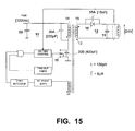
- FIG. 13 shows a variant of the Figure 8 flyback connverter in which the turn-on of the MOSFET 16 is controlled to occur at this minimum voltage point of the MOSFET drain voltage.
- Figure 14 shows the V gs , I d , V ds and I rect waveforms for the Figure 13 converter.
- the falling edge of the waveform can be seen to be sinusoidal in form, this being the voltage swing occuring at frequency F O immediately following discharge of the transformer core.
- the minimum of this voltage swing is sensed in the Figure 13 converter by an arrangment comprising a sensing coil 60 wound on the transformer core, an integrator 61 that effectively shifts the sinusoidal swing through a 90° phase shift, and a zero crossing detector 62 that detects the zero crossing of the integrator output, these zero-crossings corresponding to minimums of the sensed waveform.
- the output of the zero-crossing detector takes the form of a trigger signal fed via an OR circuit 63 to an on-time control block 64 to initiate turn on of the MOSFET 16.
- the actual on-time duration is determined by the level of the fedback output voltage, again with the objective of keeping the latter constant.
- the MOSFET 16 is no longer switched on and off at a fixed frequency, the switching frequency now being effectively load dependent. It may also be noted that it is inherent in the operation of the Figure 13 converter that it operates at the boundary between continuous and discontinuous modes of operation; accordingly, the current I rect through the diode 18 falls to zero just before the MOSFET 16 is turned on again.
- a time-out circuit 65 is provided to ensure that a turn-on trigger signal is fed to the on-time control block a predetermined time after the gate signal V gs was last high, unless the MOSFET is earlier turned on again by a trigger signal from the zero-crossing detector 62.
- FIG 15 shows an implementation of the Figure 13 converter with example values of the key components. Attention is drawn to the arrangement of the primary and secondary tuning capacitances C and C'.
- the primary tuning capacitance C which in Figure 13 was represented as provided by the capacitor 30 connected across the primary winding 14, is provided by a capacitor 30A across winding 14 together with the source-drain capacitance 30B of the MOSFET 16.
- This latter capacitance 30B is in ac terms in parallel with the capacitor 30A (reservoir capacitor 69 ensuring this); if the value of capacitance 30B is sufficient, the capacitor 30A can be dispensed with entirely.
- this capacitance C' is provided by a capacitor 35A connected across the diode 18.
- this arrangement is equivalent in ac terms to connecting the capacitor in parallel with the secondary winding 15 (it may be noted that capacitor 19 is large enough that even though it is in series with the capacitor 35A when the diode is off, its impedance can be ignored; additionally, when the diode is on, the capacitor provides an effective ac short).
- a combination of capacitors connected across the secondary winding 15 and diode 18 can also be used to provide capacitance C'.
- the capacitance C' can be distributed between these output circuits.
- Figures 16 and 17 show oscillograms of the drain voltage of MOSFET 16 for the Figure 15 converter, the Figure 16 waveform being for the case where the secondary tuning capacitor has been disconnected so that substantial ringing is exhibited as for the Figure 4 converter.
- the Figure 17 oscillogram is for the case where the secondary tuning capacitor is connected and, as can be seen, the ringing has largely disappeared.
- Figures 16 and 17 also clearly show the sinusoidal form of the falling edge of the waveform.
- the switching device 14 is controlled in the same manner as for the circuit of Figure 13 and the voltage waveforms on the drain of the MOSFET switching device and across the secondary winding are substantially the same as for the Figure 13 circuit.
- the effect of the tuning capacitors 30 and 35 is also the same as for the Figure 13 circuit (note that because in ac terms the primary winding 14 is effectively in parallel with the inductor 70, connecting the tuning capacitor 30 across the inductor 70 rather than across the primary winding, does not affect the action of the tuning capacitor).
- the Figure 18 circuit is particularly useful in giving good power factor characteristics when used to provide a regulated dc output from a rectified ac mains input.
- the capacitor 71 is chosen with a value to block mains ripple; even so, it will generally be necessary to include a low pass filter in the output-voltage feedback loop.
- the basic arrangement of the Figure 18 circuit forms the subject matter of our co-pending European Patent Application of the same date entitled "Switched Mode Power Supply with Power Factor Correction". Reference is directed to that application for a more detailed description of the operation of the Figure 18 circuit.
Abstract
Description
- with the output-circuit diode in a conducting state a first resonant circuit is formed, with resonant frequency FR, in which the primary leakage inductance and the first tuning capacitance play significant parts, and
- with the output-circuit diode in a non-conducting state a second resonant circuit is formed, with resonant frequency substantially equal to the frequency FR, in which the primary leakage inductance and the second tuning capacitance play significant parts but for which there exists a voltage/current phase relationship either side of resonance that is anti-phase to that for the first resonant circuit;
- . Figure 1
- is a circuit diagram of a known flyback converter;
- . Figure 2
- shows voltage and current time plots illustrating operation of the Figure 1 converter;
- . Figure 3
- is a diagram illustrating the use of a tuned tank coil for transferring power between inductors with limited coupling;
- . Figure 4
- is a circuit diagram of a flyback converter provided with a tuning capacitor across its transformer primary winding to cause a ringing effect with the primary leakage inductance of the converter transformer;
- . Figure 5
- shows voltage and current time plots illustrating operation of the Figure 4 converter;
- . Figure 6
- is a simplified equivalent circuit for the transformer and tuning capacitor arrangement of the Figure 4 flyback converter;
- . Figure 7
- is a diagram illustrating the phase response of the Figure 4 circuit as viewed across the transformer primary;
- . Figure 8
- is a circuit diagram of a first form of flyback converter embodying the invention, this converter being provided with tuning capacitors across both its primary and secondary windings and a non-linear device in its output circuit, the non-linear device being constituted by the output circuit diode;
- . Figure 9
- is a simplified equivalent circuit for the transformer and tuning capacitor arrangement of the Figure 8 flyback converter;
- . Figure 10
- is a diagram illustrating the phase response of the Figure 8 circuit as viewed across the transformer primary;
- . Figure 11
- is a diagram illustrating the effect of the non-linear component in the output circuit of the Figure 8 converter;
- . Figure 12
- is a circuit diagram of a second form of flyback converter embodying the invention, this converter being similar to that shown in Figure 8 but with a MOSFET used as the non-linear device in the converter output circuit;
- . Figure 13
- is a circuit diagram of a third form of flyback converter embodying the invention, this converter being similar to that shown in Figure 8 but with turn on of the input-circuit switching device being controlled to occur at minimums of the voltage across the device;
- . Figure 14
- shows voltage and current time plots illustrating operation of the Figure 13 circuit;
- . Figure 15
- is a circuit diagram of an implementation of the Figure 13 circuit;
- . Figure 16
- is a voltage/time graph showing the voltage across the input-circuit switching device for the Figure 15 circuit but with the secondary tuning capacitor removed;
- . Figure 17
- is a voltage/time graph similar to Figure 16 but with the secondary tuning capacitor connected; and
- . Figure 18
- is a circuit diagram of a variant of the Figure 13 circuit showing a different connection arrangement for the input circuit switching devices.
Claims (11)
- A flyback converter comprising an input circuit (11) coupled to an output circuit (10) through an energy storing transformer (13) that has primary and secondary windings (14,15) each with main and leakage inductances; the input circuit (11) comprising a switching device (16) connected to regulate energisation of said primary winding (14), and control means (17) for controlling the cyclic turning on and off of the switching device (16); and the output circuit (12) comprising a diode (18) connected in series with said secondary winding (15), and a reservoir capacitor (19) connected in parallel with the series combination of the secondary winding (15) and diode (18) and across which the converter output is produced; characterised in that a first tuning capacitance (30) is provided in the input circuit (11) either physically connected in parallel with the primary winding (14) or in a position that in terms of a.c. functional effect is equivalent to such a parallel connection, and in that a second tuning capacitance (35) is provided in the output circuit (12) either physically connected in parallel with said secondary winding (15) or in a position that in terms of a.c. functional effect is equivalent to such a parallel connection, these tuning capacitances (30,35) having values such that:the output circuit including a non-linear device (18;50) operative to combine the anti-phase components of ringing produced by said first and second resonant circuits following turn off of the switching device (16), whereby energy stored in the primary leakage inductance is at least partially transferred to the output circuit (12) and converted into a dc component of the converter output.with the diode (18) in a conducting state a first resonant circuit is formed, with resonant frequency FR, in which the primary leakage inductance and said first tuning capacitance (14) play significant parts, andwith the diode (18) in a non-conducting state a second resonant circuit is formed, with resonant frequency substantially equal to said frequency FR, in which the primary leakage inductance and said second tuning capacitance (35) play significant parts but for which there exists a voltage/current phase relationship either side of resonance that is anti-phase to that for said first resonant circuit;
- A flyback converter according to claim 1, wherein said switching device (16) is a MOSFET and said first tuning capacitance (30) is provided at least in part by the drain-source capacitance (30B) of the MOSFET.
- A flyback converter according to claim 1, wherein said second tuning capacitance (35) is provided at least in part by a capacitor (35A) connected across said diode (18).
- A flyback converter according to claim 1, wherein the converter is provided with multiple said output circuits (12) each coupled to said primary winding (14) through a respective said secondary winding (15) of the transformer (13); said second tuning capacitance (35) being divided between said output circuits (12).
- A flyback converter according to claim 1, wherein said non-linear device is constituted by said diode (18).
- A flyback converter according to claim 1, wherein said non-linear device comprises a MOSFET (50) connected in series with said diode (18), and means (51) for switching the MOSFET (50) on and off at synchronism with said ringing.
- A flyback converter according to claim 1, wherein said control means (17) comprises sensing means (60) for sensing the voltage across the switching device (16) when the latter is off, determining means (61,62) for determining a minimum of the voltage sensed by said sensing means, and turn-on means (64) for turning on the switching device (16) at a said minimum of the voltage thereacross as determined by said determining means.
- A flyback converter according to claim 7, wherein said sensing means comprises a sensing winding (60) wound jointly with said primary and secondary windings (14,15), and said determining means comprises integration means (61) for integrating the voltage sensed by said sensing winding (60), and means (62) for detecting a zero crossing of the voltage integrated by said integration means, this zero crossing being indicative of the said minimum of the voltage across the switching device (16).
- A flyback converter according to claim 7, wherein said control means (17) further comprises means for controlling the duration of the on time of the switching device (16) in dependence on the voltage produced at the output of the converter such as to maintain the converter output voltage substantially constant.
- A flyback converter according to claim 7, wherein said control means (17) further comprises time-out means (65) for initiating turn on of the switching device (16) a predetermined time after when switching device (16) was last on unless the latter is earlier turned on again by said turn-on means (64).
- A flyback converter according to claim 7, wherein said input circuit (11) further comprises an inductor (70) connected in series with said switching device (16), and a capacitor (71) connected in series with said primary winding (14) across the switching device (16).
Priority Applications (6)
| Application Number | Priority Date | Filing Date | Title |
|---|---|---|---|
| DE69506096T DE69506096T2 (en) | 1995-07-31 | 1995-07-31 | Flyback converter |
| EP95410075A EP0757428B1 (en) | 1995-07-31 | 1995-07-31 | Flyback converter |
| AT95410075T ATE173569T1 (en) | 1995-07-31 | 1995-07-31 | FLYBACK CONVERTER |
| US08/675,300 US5608613A (en) | 1995-07-31 | 1996-07-01 | Flyback converter |
| KR1019960030803A KR100398565B1 (en) | 1995-07-31 | 1996-07-27 | Flyback converter |
| JP20047496A JP3652798B2 (en) | 1995-07-31 | 1996-07-30 | Flyback converter |
Applications Claiming Priority (1)
| Application Number | Priority Date | Filing Date | Title |
|---|---|---|---|
| EP95410075A EP0757428B1 (en) | 1995-07-31 | 1995-07-31 | Flyback converter |
Publications (2)
| Publication Number | Publication Date |
|---|---|
| EP0757428A1 EP0757428A1 (en) | 1997-02-05 |
| EP0757428B1 true EP0757428B1 (en) | 1998-11-18 |
Family
ID=8221561
Family Applications (1)
| Application Number | Title | Priority Date | Filing Date |
|---|---|---|---|
| EP95410075A Expired - Lifetime EP0757428B1 (en) | 1995-07-31 | 1995-07-31 | Flyback converter |
Country Status (6)
| Country | Link |
|---|---|
| US (1) | US5608613A (en) |
| EP (1) | EP0757428B1 (en) |
| JP (1) | JP3652798B2 (en) |
| KR (1) | KR100398565B1 (en) |
| AT (1) | ATE173569T1 (en) |
| DE (1) | DE69506096T2 (en) |
Cited By (5)
| Publication number | Priority date | Publication date | Assignee | Title |
|---|---|---|---|---|
| US8023290B2 (en) | 1997-01-24 | 2011-09-20 | Synqor, Inc. | High efficiency power converter |
| US10199950B1 (en) | 2013-07-02 | 2019-02-05 | Vlt, Inc. | Power distribution architecture with series-connected bus converter |
| RU2692466C1 (en) * | 2018-08-17 | 2019-06-25 | Общество с ограниченной ответственностью "Научно-производственная фирма "Плазмаинформ" | Quasi-resonance constant voltage converter with low pulsations of output voltage during operation in conditions of high negative temperatures |
| RU191122U1 (en) * | 2018-07-06 | 2019-07-25 | Общество с ограниченной ответственностью "Научно-производственная фирма "Плазмаинформ" | Quasi-resonant DC voltage converter with low ripple output voltage when operating in conditions of high negative temperatures |
| CN110417288A (en) * | 2019-08-06 | 2019-11-05 | 珠海格力电器股份有限公司 | A kind of novel switched power driving circuit and its control method |
Families Citing this family (40)
| Publication number | Priority date | Publication date | Assignee | Title |
|---|---|---|---|---|
| FR2738418B1 (en) * | 1995-09-01 | 1997-11-21 | Lacme | ELECTRICAL TRANSFORMER DEVICE WHOSE PRIMARY IS SUPPLIED UNDER CONTROL OF A CHOPPER |
| US5822200A (en) * | 1997-04-21 | 1998-10-13 | Nt International, Inc. | Low level, high efficiency DC/DC converter |
| JPH1155943A (en) * | 1997-06-02 | 1999-02-26 | Murata Mfg Co Ltd | Switching power unit |
| IT1308452B1 (en) * | 1999-04-23 | 2001-12-17 | Fiat Ricerche | RESONANT TRANSITION DC-DC CONVERTER AND CONTROL METHOD OF RESONANT TRANSITION OF A DC-DC CONVERTER |
| JP2000324831A (en) * | 1999-05-11 | 2000-11-24 | Sony Corp | Switching power supply circuit |
| US6292069B1 (en) * | 1999-09-14 | 2001-09-18 | Eaton Corporation | Loosely coupled rotary transformer having resonant circuit |
| TW507414B (en) * | 1999-10-29 | 2002-10-21 | Sony Corp | Switching power circuit with secondary side parallel and series resonance |
| US6166926A (en) * | 2000-01-11 | 2000-12-26 | Thomson Licensing S.A. | Zero voltage switching power supply with burst mode |
| EP1281233A1 (en) | 2000-05-11 | 2003-02-05 | Sony Corporation | Switching power supply circuit |
| DE60142233D1 (en) | 2000-06-27 | 2010-07-08 | Nxp Bv | COMMUNICATION DEVICE FOR DETERMINING THE ORDER OF PREVIOUS DATA CARRIER |
| US6285567B1 (en) * | 2000-09-14 | 2001-09-04 | Honeywell International Inc. | Methods and apparatus for utilizing the transformer leakage energy in a power supply |
| US6594161B2 (en) * | 2000-11-11 | 2003-07-15 | Minebea Co., Ltd. | Power converter having independent primary and secondary switches |
| US6341073B1 (en) | 2000-11-16 | 2002-01-22 | Philips Electronics North America Corporation | Multiple valley controller for switching circuit |
| US6421256B1 (en) | 2001-06-25 | 2002-07-16 | Koninklijke Philips Electronics N.V. | Method for reducing mains harmonics and switching losses in discontinuous-mode, switching power converters |
| US6671189B2 (en) * | 2001-11-09 | 2003-12-30 | Minebea Co., Ltd. | Power converter having primary and secondary side switches |
| US6989656B2 (en) * | 2002-05-13 | 2006-01-24 | Jam Technologies, Llc | Flyback converter linearization methods and apparatus |
| EP1437824A1 (en) * | 2003-01-09 | 2004-07-14 | Fabrice Barthélémy | Voltage converter suited for supplying multiple very low security DC-voltages. |
| US20060097652A1 (en) * | 2003-01-14 | 2006-05-11 | Koninklijke Philips Electronics N.V. | Circuit and method for providing power to a load, especially a high-intensity discharge lamp |
| US6995991B1 (en) * | 2004-07-20 | 2006-02-07 | System General Corp. | PWM controller for synchronous rectifier of flyback power converter |
| DE102005028402A1 (en) | 2005-06-20 | 2006-12-21 | Austriamicrosystems Ag | Control arrangement for switching configuration has metal oxide semiconductor field effect transistor (MOSFET) having control connection connected to control circuit output |
| KR100813979B1 (en) * | 2005-07-26 | 2008-03-14 | 삼성전자주식회사 | Power supply device having multiple outputs |
| TW200721653A (en) * | 2005-09-02 | 2007-06-01 | Sony Corp | Switching power supply circuit |
| US20070152642A1 (en) * | 2006-01-03 | 2007-07-05 | Franklin Philip G | Wireless glass-mounted lighting fixtures |
| US7738266B2 (en) | 2006-05-26 | 2010-06-15 | Cambridge Semiconductor Limited | Forward power converter controllers |
| GB0610422D0 (en) * | 2006-05-26 | 2006-07-05 | Cambridge Semiconductor Ltd | Forward power converters |
| KR101009333B1 (en) | 2008-11-18 | 2011-01-19 | 한국전기연구원 | High DC voltage generator and High voltage calibration waveform generator for impulse measurement device |
| US7876584B2 (en) * | 2009-06-24 | 2011-01-25 | Alpha And Omega Semiconductor Incorporated | Circuit and method for controlling the secondary FET of transformer coupled synchronous rectified flyback converter |
| US8964420B2 (en) | 2011-12-13 | 2015-02-24 | Apple Inc. | Zero voltage switching in flyback converters with variable input voltages |
| CN102664526B (en) * | 2012-05-15 | 2015-12-16 | 迈象电子科技(上海)有限公司 | The method of reverse excitation circuit and the loss of reduction reverse excitation circuit transformer leakage inductance |
| TWI496406B (en) | 2012-07-03 | 2015-08-11 | System General Corp | Power converter and method for controlling power converter |
| US8897038B2 (en) * | 2012-07-31 | 2014-11-25 | Dialog Semiconductor Inc. | Switching power converter dynamic load detection |
| TW201414167A (en) * | 2012-09-26 | 2014-04-01 | Phihong Technology Co Ltd | Controller with quasi-resonant mode and continuous conduction mode and operating method thereof |
| JP5802647B2 (en) * | 2012-12-20 | 2015-10-28 | 株式会社タムラ製作所 | Switching element drive system |
| JP5765591B2 (en) | 2013-04-18 | 2015-08-19 | 株式会社デンソー | Power supply |
| JP5931013B2 (en) * | 2013-07-04 | 2016-06-08 | Fdk株式会社 | Synchronous rectification power supply |
| KR101516088B1 (en) * | 2013-11-28 | 2015-05-06 | 주식회사 포스코아이씨티 | H-Bridge Inverter Module and Multi Level Inverter Using H-Bridge Inverter Module |
| FR3020523B1 (en) * | 2014-04-29 | 2016-05-06 | Valeo Systemes De Controle Moteur | ELECTRICAL POWER SUPPLY AND METHOD FOR CONTROLLING AN ELECTRIC POWER SUPPLY |
| CN104362856B (en) * | 2014-11-05 | 2016-08-24 | 无锡中汇汽车电子科技有限公司 | A kind of control method of Zero-voltage switch flyback changer |
| US10756640B1 (en) | 2019-03-28 | 2020-08-25 | Appulse Power Inc. | Flyback converter with synchronous rectifier controller |
| US20230216417A1 (en) * | 2020-05-29 | 2023-07-06 | Luis LEON LARA | Flyback converter with indirect estimation of primary- side voltage at the secondary-side |
Family Cites Families (10)
| Publication number | Priority date | Publication date | Assignee | Title |
|---|---|---|---|---|
| US4631652A (en) * | 1984-11-30 | 1986-12-23 | Rca Corporation | Frequency controlled resonant regulator |
| JPS61218368A (en) * | 1985-03-20 | 1986-09-27 | Murata Mfg Co Ltd | Stabilized high voltage power source |
| US4785387A (en) * | 1986-04-28 | 1988-11-15 | Virginia Tech Intellectual Properties, Inc. | Resonant converters with secondary-side resonance |
| US4764857A (en) * | 1987-05-06 | 1988-08-16 | Zenith Electronics Corporation | Power supply start-up circuit with high frequency transformer |
| CA2019525C (en) * | 1989-06-23 | 1995-07-11 | Takuya Ishii | Switching power supply device |
| JPH04217862A (en) * | 1990-01-29 | 1992-08-07 | Toshiba Corp | Current resonance converter |
| US5396410A (en) * | 1990-01-31 | 1995-03-07 | Kabushiki Kaisha Toshiba | Zero current switching resonant converter |
| JPH04150767A (en) * | 1990-10-08 | 1992-05-25 | Fuji Electric Co Ltd | Switching power supply circuit |
| JP3419797B2 (en) * | 1992-01-10 | 2003-06-23 | 松下電器産業株式会社 | Switching power supply |
| JPH06209569A (en) * | 1993-01-05 | 1994-07-26 | Yokogawa Electric Corp | Switching power supply |
-
1995
- 1995-07-31 AT AT95410075T patent/ATE173569T1/en not_active IP Right Cessation
- 1995-07-31 EP EP95410075A patent/EP0757428B1/en not_active Expired - Lifetime
- 1995-07-31 DE DE69506096T patent/DE69506096T2/en not_active Expired - Fee Related
-
1996
- 1996-07-01 US US08/675,300 patent/US5608613A/en not_active Expired - Lifetime
- 1996-07-27 KR KR1019960030803A patent/KR100398565B1/en not_active IP Right Cessation
- 1996-07-30 JP JP20047496A patent/JP3652798B2/en not_active Expired - Fee Related
Cited By (11)
| Publication number | Priority date | Publication date | Assignee | Title |
|---|---|---|---|---|
| US8023290B2 (en) | 1997-01-24 | 2011-09-20 | Synqor, Inc. | High efficiency power converter |
| US8493751B2 (en) | 1997-01-24 | 2013-07-23 | Synqor, Inc. | High efficiency power converter |
| US9143042B2 (en) | 1997-01-24 | 2015-09-22 | Synqor, Inc. | High efficiency power converter |
| US10199950B1 (en) | 2013-07-02 | 2019-02-05 | Vlt, Inc. | Power distribution architecture with series-connected bus converter |
| US10594223B1 (en) | 2013-07-02 | 2020-03-17 | Vlt, Inc. | Power distribution architecture with series-connected bus converter |
| US11075583B1 (en) | 2013-07-02 | 2021-07-27 | Vicor Corporation | Power distribution architecture with series-connected bus converter |
| US11705820B2 (en) | 2013-07-02 | 2023-07-18 | Vicor Corporation | Power distribution architecture with series-connected bus converter |
| RU191122U1 (en) * | 2018-07-06 | 2019-07-25 | Общество с ограниченной ответственностью "Научно-производственная фирма "Плазмаинформ" | Quasi-resonant DC voltage converter with low ripple output voltage when operating in conditions of high negative temperatures |
| RU2692466C1 (en) * | 2018-08-17 | 2019-06-25 | Общество с ограниченной ответственностью "Научно-производственная фирма "Плазмаинформ" | Quasi-resonance constant voltage converter with low pulsations of output voltage during operation in conditions of high negative temperatures |
| CN110417288A (en) * | 2019-08-06 | 2019-11-05 | 珠海格力电器股份有限公司 | A kind of novel switched power driving circuit and its control method |
| CN110417288B (en) * | 2019-08-06 | 2021-01-15 | 珠海格力电器股份有限公司 | Novel switching power supply driving circuit and control method thereof |
Also Published As
| Publication number | Publication date |
|---|---|
| JP3652798B2 (en) | 2005-05-25 |
| JPH09107676A (en) | 1997-04-22 |
| DE69506096D1 (en) | 1998-12-24 |
| EP0757428A1 (en) | 1997-02-05 |
| KR100398565B1 (en) | 2004-04-14 |
| DE69506096T2 (en) | 1999-04-15 |
| US5608613A (en) | 1997-03-04 |
| KR970008238A (en) | 1997-02-24 |
| ATE173569T1 (en) | 1998-12-15 |
Similar Documents
| Publication | Publication Date | Title |
|---|---|---|
| EP0757428B1 (en) | Flyback converter | |
| US6061252A (en) | Switching power supply device | |
| JP3475925B2 (en) | Switching power supply | |
| CN103178719B (en) | Multi-voltage power supply | |
| JP3475887B2 (en) | Switching power supply | |
| EP0658968B1 (en) | Switching regulator | |
| US8817497B2 (en) | Switching power converter for reducing EMI from ring oscillation and its control method | |
| US7295449B2 (en) | Simple switched-mode power supply with current and voltage limitation | |
| TWI732581B (en) | Conversion device with oscillation reduction control and method of operation of oscillation reduction control the same | |
| JP2002084753A (en) | Multiple-output switching power supply unit | |
| JP3653075B2 (en) | Switching power transmission device | |
| EP1032968B1 (en) | Switched-mode power supply | |
| CA2307441A1 (en) | Zero voltage switched power supply converter | |
| US6975097B2 (en) | Unitary magnetic coupler and switch mode power supply | |
| CA2214217C (en) | Switching power supply apparatus | |
| CN112072922B (en) | Conversion device with shock absorption control and operation method of shock absorption control thereof | |
| JP4253808B2 (en) | Switching power supply | |
| GB2456599A (en) | Resonant discontinuous forward power converter | |
| CA2220747A1 (en) | Dc-dc converters | |
| KR19990065926A (en) | Lossless snubber circuit for soft switching of booster AC / DC converters and full bridge DC / DC converters | |
| AU737397B2 (en) | Lossless active clamp for secondary circuits | |
| KR100258755B1 (en) | Apparatus for power supply in isdn network terminal | |
| JPH1066335A (en) | Converter circuit | |
| KR20040031503A (en) | Snuber circuit and Switching Mode Power Supply thereof | |
| JP2006304471A (en) | Self-excited type switching power supply device |
Legal Events
| Date | Code | Title | Description |
|---|---|---|---|
| PUAI | Public reference made under article 153(3) epc to a published international application that has entered the european phase |
Free format text: ORIGINAL CODE: 0009012 |
|
| AK | Designated contracting states |
Kind code of ref document: A1 Designated state(s): AT DE FR GB IT NL SE |
|
| 17P | Request for examination filed |
Effective date: 19970714 |
|
| 17Q | First examination report despatched |
Effective date: 19971020 |
|
| GRAG | Despatch of communication of intention to grant |
Free format text: ORIGINAL CODE: EPIDOS AGRA |
|
| GRAG | Despatch of communication of intention to grant |
Free format text: ORIGINAL CODE: EPIDOS AGRA |
|
| GRAH | Despatch of communication of intention to grant a patent |
Free format text: ORIGINAL CODE: EPIDOS IGRA |
|
| GRAH | Despatch of communication of intention to grant a patent |
Free format text: ORIGINAL CODE: EPIDOS IGRA |
|
| GRAH | Despatch of communication of intention to grant a patent |
Free format text: ORIGINAL CODE: EPIDOS IGRA |
|
| GRAA | (expected) grant |
Free format text: ORIGINAL CODE: 0009210 |
|
| AK | Designated contracting states |
Kind code of ref document: B1 Designated state(s): AT DE FR GB IT NL SE |
|
| PG25 | Lapsed in a contracting state [announced via postgrant information from national office to epo] |
Ref country code: SE Free format text: THE PATENT HAS BEEN ANNULLED BY A DECISION OF A NATIONAL AUTHORITY Effective date: 19981118 Ref country code: AT Free format text: LAPSE BECAUSE OF FAILURE TO SUBMIT A TRANSLATION OF THE DESCRIPTION OR TO PAY THE FEE WITHIN THE PRESCRIBED TIME-LIMIT Effective date: 19981118 |
|
| REF | Corresponds to: |
Ref document number: 173569 Country of ref document: AT Date of ref document: 19981215 Kind code of ref document: T |
|
| REF | Corresponds to: |
Ref document number: 69506096 Country of ref document: DE Date of ref document: 19981224 |
|
| ET | Fr: translation filed | ||
| PLBE | No opposition filed within time limit |
Free format text: ORIGINAL CODE: 0009261 |
|
| STAA | Information on the status of an ep patent application or granted ep patent |
Free format text: STATUS: NO OPPOSITION FILED WITHIN TIME LIMIT |
|
| 26N | No opposition filed | ||
| REG | Reference to a national code |
Ref country code: GB Ref legal event code: 732E |
|
| NLS | Nl: assignments of ep-patents |
Owner name: HEWLETT-PACKARD COMPANY (A DELAWARE CORPORATION) |
|
| REG | Reference to a national code |
Ref country code: GB Ref legal event code: IF02 |
|
| REG | Reference to a national code |
Ref country code: FR Ref legal event code: TP |
|
| PGFP | Annual fee paid to national office [announced via postgrant information from national office to epo] |
Ref country code: DE Payment date: 20070831 Year of fee payment: 13 |
|
| PGFP | Annual fee paid to national office [announced via postgrant information from national office to epo] |
Ref country code: GB Payment date: 20070727 Year of fee payment: 13 |
|
| PGFP | Annual fee paid to national office [announced via postgrant information from national office to epo] |
Ref country code: NL Payment date: 20070724 Year of fee payment: 13 Ref country code: IT Payment date: 20070727 Year of fee payment: 13 |
|
| PGFP | Annual fee paid to national office [announced via postgrant information from national office to epo] |
Ref country code: FR Payment date: 20070717 Year of fee payment: 13 |
|
| GBPC | Gb: european patent ceased through non-payment of renewal fee |
Effective date: 20080731 |
|
| NLV4 | Nl: lapsed or anulled due to non-payment of the annual fee |
Effective date: 20090201 |
|
| PG25 | Lapsed in a contracting state [announced via postgrant information from national office to epo] |
Ref country code: DE Free format text: LAPSE BECAUSE OF NON-PAYMENT OF DUE FEES Effective date: 20090203 |
|
| REG | Reference to a national code |
Ref country code: FR Ref legal event code: ST Effective date: 20090331 |
|
| PG25 | Lapsed in a contracting state [announced via postgrant information from national office to epo] |
Ref country code: NL Free format text: LAPSE BECAUSE OF NON-PAYMENT OF DUE FEES Effective date: 20090201 |
|
| PG25 | Lapsed in a contracting state [announced via postgrant information from national office to epo] |
Ref country code: GB Free format text: LAPSE BECAUSE OF NON-PAYMENT OF DUE FEES Effective date: 20080731 |
|
| PG25 | Lapsed in a contracting state [announced via postgrant information from national office to epo] |
Ref country code: IT Free format text: LAPSE BECAUSE OF NON-PAYMENT OF DUE FEES Effective date: 20080731 Ref country code: FR Free format text: LAPSE BECAUSE OF NON-PAYMENT OF DUE FEES Effective date: 20080731 |