EP0779657A2 - Surface-mounted semiconductor package and its manufacturing method - Google Patents
Surface-mounted semiconductor package and its manufacturing method Download PDFInfo
- Publication number
- EP0779657A2 EP0779657A2 EP96118894A EP96118894A EP0779657A2 EP 0779657 A2 EP0779657 A2 EP 0779657A2 EP 96118894 A EP96118894 A EP 96118894A EP 96118894 A EP96118894 A EP 96118894A EP 0779657 A2 EP0779657 A2 EP 0779657A2
- Authority
- EP
- European Patent Office
- Prior art keywords
- semiconductor package
- substrate
- mounted semiconductor
- slots
- metallic coating
- Prior art date
- Legal status (The legal status is an assumption and is not a legal conclusion. Google has not performed a legal analysis and makes no representation as to the accuracy of the status listed.)
- Withdrawn
Links
Images


Classifications
-
- H—ELECTRICITY
- H05—ELECTRIC TECHNIQUES NOT OTHERWISE PROVIDED FOR
- H05K—PRINTED CIRCUITS; CASINGS OR CONSTRUCTIONAL DETAILS OF ELECTRIC APPARATUS; MANUFACTURE OF ASSEMBLAGES OF ELECTRICAL COMPONENTS
- H05K3/00—Apparatus or processes for manufacturing printed circuits
-
- H—ELECTRICITY
- H01—ELECTRIC ELEMENTS
- H01L—SEMICONDUCTOR DEVICES NOT COVERED BY CLASS H10
- H01L23/00—Details of semiconductor or other solid state devices
- H01L23/28—Encapsulations, e.g. encapsulating layers, coatings, e.g. for protection
- H01L23/31—Encapsulations, e.g. encapsulating layers, coatings, e.g. for protection characterised by the arrangement or shape
- H01L23/3107—Encapsulations, e.g. encapsulating layers, coatings, e.g. for protection characterised by the arrangement or shape the device being completely enclosed
- H01L23/3121—Encapsulations, e.g. encapsulating layers, coatings, e.g. for protection characterised by the arrangement or shape the device being completely enclosed a substrate forming part of the encapsulation
- H01L23/3128—Encapsulations, e.g. encapsulating layers, coatings, e.g. for protection characterised by the arrangement or shape the device being completely enclosed a substrate forming part of the encapsulation the substrate having spherical bumps for external connection
-
- H—ELECTRICITY
- H01—ELECTRIC ELEMENTS
- H01L—SEMICONDUCTOR DEVICES NOT COVERED BY CLASS H10
- H01L23/00—Details of semiconductor or other solid state devices
- H01L23/02—Containers; Seals
- H01L23/04—Containers; Seals characterised by the shape of the container or parts, e.g. caps, walls
- H01L23/053—Containers; Seals characterised by the shape of the container or parts, e.g. caps, walls the container being a hollow construction and having an insulating or insulated base as a mounting for the semiconductor body
- H01L23/055—Containers; Seals characterised by the shape of the container or parts, e.g. caps, walls the container being a hollow construction and having an insulating or insulated base as a mounting for the semiconductor body the leads having a passage through the base
-
- H—ELECTRICITY
- H01—ELECTRIC ELEMENTS
- H01L—SEMICONDUCTOR DEVICES NOT COVERED BY CLASS H10
- H01L23/00—Details of semiconductor or other solid state devices
- H01L23/02—Containers; Seals
- H01L23/10—Containers; Seals characterised by the material or arrangement of seals between parts, e.g. between cap and base of the container or between leads and walls of the container
-
- H—ELECTRICITY
- H01—ELECTRIC ELEMENTS
- H01L—SEMICONDUCTOR DEVICES NOT COVERED BY CLASS H10
- H01L2224/00—Indexing scheme for arrangements for connecting or disconnecting semiconductor or solid-state bodies and methods related thereto as covered by H01L24/00
- H01L2224/01—Means for bonding being attached to, or being formed on, the surface to be connected, e.g. chip-to-package, die-attach, "first-level" interconnects; Manufacturing methods related thereto
- H01L2224/42—Wire connectors; Manufacturing methods related thereto
- H01L2224/47—Structure, shape, material or disposition of the wire connectors after the connecting process
- H01L2224/48—Structure, shape, material or disposition of the wire connectors after the connecting process of an individual wire connector
- H01L2224/4805—Shape
- H01L2224/4809—Loop shape
- H01L2224/48091—Arched
-
- H—ELECTRICITY
- H01—ELECTRIC ELEMENTS
- H01L—SEMICONDUCTOR DEVICES NOT COVERED BY CLASS H10
- H01L2224/00—Indexing scheme for arrangements for connecting or disconnecting semiconductor or solid-state bodies and methods related thereto as covered by H01L24/00
- H01L2224/01—Means for bonding being attached to, or being formed on, the surface to be connected, e.g. chip-to-package, die-attach, "first-level" interconnects; Manufacturing methods related thereto
- H01L2224/42—Wire connectors; Manufacturing methods related thereto
- H01L2224/47—Structure, shape, material or disposition of the wire connectors after the connecting process
- H01L2224/48—Structure, shape, material or disposition of the wire connectors after the connecting process of an individual wire connector
- H01L2224/481—Disposition
- H01L2224/48151—Connecting between a semiconductor or solid-state body and an item not being a semiconductor or solid-state body, e.g. chip-to-substrate, chip-to-passive
- H01L2224/48221—Connecting between a semiconductor or solid-state body and an item not being a semiconductor or solid-state body, e.g. chip-to-substrate, chip-to-passive the body and the item being stacked
- H01L2224/48225—Connecting between a semiconductor or solid-state body and an item not being a semiconductor or solid-state body, e.g. chip-to-substrate, chip-to-passive the body and the item being stacked the item being non-metallic, e.g. insulating substrate with or without metallisation
- H01L2224/48227—Connecting between a semiconductor or solid-state body and an item not being a semiconductor or solid-state body, e.g. chip-to-substrate, chip-to-passive the body and the item being stacked the item being non-metallic, e.g. insulating substrate with or without metallisation connecting the wire to a bond pad of the item
-
- H—ELECTRICITY
- H01—ELECTRIC ELEMENTS
- H01L—SEMICONDUCTOR DEVICES NOT COVERED BY CLASS H10
- H01L24/00—Arrangements for connecting or disconnecting semiconductor or solid-state bodies; Methods or apparatus related thereto
- H01L24/01—Means for bonding being attached to, or being formed on, the surface to be connected, e.g. chip-to-package, die-attach, "first-level" interconnects; Manufacturing methods related thereto
- H01L24/42—Wire connectors; Manufacturing methods related thereto
- H01L24/47—Structure, shape, material or disposition of the wire connectors after the connecting process
- H01L24/48—Structure, shape, material or disposition of the wire connectors after the connecting process of an individual wire connector
-
- H—ELECTRICITY
- H01—ELECTRIC ELEMENTS
- H01L—SEMICONDUCTOR DEVICES NOT COVERED BY CLASS H10
- H01L2924/00—Indexing scheme for arrangements or methods for connecting or disconnecting semiconductor or solid-state bodies as covered by H01L24/00
- H01L2924/0001—Technical content checked by a classifier
- H01L2924/00014—Technical content checked by a classifier the subject-matter covered by the group, the symbol of which is combined with the symbol of this group, being disclosed without further technical details
-
- H—ELECTRICITY
- H01—ELECTRIC ELEMENTS
- H01L—SEMICONDUCTOR DEVICES NOT COVERED BY CLASS H10
- H01L2924/00—Indexing scheme for arrangements or methods for connecting or disconnecting semiconductor or solid-state bodies as covered by H01L24/00
- H01L2924/01—Chemical elements
- H01L2924/01078—Platinum [Pt]
-
- H—ELECTRICITY
- H01—ELECTRIC ELEMENTS
- H01L—SEMICONDUCTOR DEVICES NOT COVERED BY CLASS H10
- H01L2924/00—Indexing scheme for arrangements or methods for connecting or disconnecting semiconductor or solid-state bodies as covered by H01L24/00
- H01L2924/15—Details of package parts other than the semiconductor or other solid state devices to be connected
- H01L2924/151—Die mounting substrate
- H01L2924/153—Connection portion
- H01L2924/1531—Connection portion the connection portion being formed only on the surface of the substrate opposite to the die mounting surface
- H01L2924/15311—Connection portion the connection portion being formed only on the surface of the substrate opposite to the die mounting surface being a ball array, e.g. BGA
-
- H—ELECTRICITY
- H01—ELECTRIC ELEMENTS
- H01L—SEMICONDUCTOR DEVICES NOT COVERED BY CLASS H10
- H01L2924/00—Indexing scheme for arrangements or methods for connecting or disconnecting semiconductor or solid-state bodies as covered by H01L24/00
- H01L2924/15—Details of package parts other than the semiconductor or other solid state devices to be connected
- H01L2924/161—Cap
- H01L2924/1615—Shape
- H01L2924/16152—Cap comprising a cavity for hosting the device, e.g. U-shaped cap
-
- H—ELECTRICITY
- H01—ELECTRIC ELEMENTS
- H01L—SEMICONDUCTOR DEVICES NOT COVERED BY CLASS H10
- H01L2924/00—Indexing scheme for arrangements or methods for connecting or disconnecting semiconductor or solid-state bodies as covered by H01L24/00
- H01L2924/15—Details of package parts other than the semiconductor or other solid state devices to be connected
- H01L2924/181—Encapsulation
Landscapes
- Engineering & Computer Science (AREA)
- Microelectronics & Electronic Packaging (AREA)
- Physics & Mathematics (AREA)
- Condensed Matter Physics & Semiconductors (AREA)
- General Physics & Mathematics (AREA)
- Computer Hardware Design (AREA)
- Power Engineering (AREA)
- Manufacturing & Machinery (AREA)
- Structures Or Materials For Encapsulating Or Coating Semiconductor Devices Or Solid State Devices (AREA)
- Printing Elements For Providing Electric Connections Between Printed Circuits (AREA)
- Structures For Mounting Electric Components On Printed Circuit Boards (AREA)
- Lead Frames For Integrated Circuits (AREA)
Abstract
The semiconductor package contains the substrate with a stacked structure; the semiconductor device mounted on the top of the substrate and provided with the electrode pads ; the input/output terminals on the bottom of the substrate, which connects the semiconductor package to the printed circuit board; and the conductive tubes going through the substrate, which connects the input/output terminals and the electrode pads. The surface-mounted semiconductor package has the protecting means on its sides. The protect means prevents water and the like from infiltrating the edges of the substrate, and additionally avoid a crack of the substrate due to expansion of the water. Furthermore, the protecting means has the pairs of lands on both sides of the substrate, which fasten the edges of the substrate.
Description
- The present invention relates to a semiconductor package, such as the surface-mounted semiconductor package, which is mounted on the surface of the printed circuit board with input/output pins not inserted thereinto, and its manufacturing method.
- Recently, more sophisticated function of a semiconductor package, such as an IC package built into electronic devices including personal computers or the like, requires more numbers of input/output pins. As a matter of fact, the number of input/output pins per package has reached a few hundred.
- One of those packages is a Quad Flat Package (QFP), where the input/output pins are arranged on four sides of the square package. However, as more and more input/output pins are used, the package must be increased in size to allow more pins to be arranged on its sides, thus requiring more space.
- In order to arrange more pins in a limited space on this type of package, reduction of the pin-to-pin pitch is necessary. However, when the package is mounted on the printed circuit board, for example, by soldering, the input/output pins to be densely arranged sometimes causes electric short therebetween.
- To solve this problem, a Ball Grid Array (BGA), shown in Figs. 10, 11(a), and 11(b), has been introduced recently as a new type of package to allow more input/output pins to be placed.
- Fig. 10 is a cross sectional view of a conventional surface-mounted semiconductor package of BGA type, and Fig. 11(a) and 11(b) are the enlarged sectional views of the part of the semiconductor package surrounded by the rectangle indicated by the symbol A in Fig. 10.
- On the semiconductor package shown in Fig. 10, the semiconductor device 1 is attached by bonding such as adhesives, in a predetermined area on the
substrate 2, which includes the stacked fibers 2a such as glass fibers bound by epoxy resin, as shown in Fig. 11(a) and Fig. 11(b). The electrode pads on the semiconductor device 1 are connected via thebonding wires 3 to theconductive patterns 4 on thesubstrate 2, and the semiconductor device 1 and thebonding wires 3 are sealed with theresin material 5. - On the bottom of the
substrate 2 are formed theconductive patterns 6 which correspond to theconductive patterns 4. The correspondingconductive patterns conductive coatings 7 formed on the inside walls of the through-holes in thesubstrate 2. With both of the semiconductor device 1 and thebonding wires 3 being sealed with theresin material 5, thebumps 8 to be made of material such as solder, are formed on theconductive pattern 6. Thebumps 8, which serve like the input/output pins of the QFP, fix the semiconductor device 1 on the printedcircuit board 9b, which an electric connection therebetween are performed. - Though the input/output pins of the QFP arranged in line on every sides of the package, the
bumps 8 of the BGA are placed on the bottom surface of the package in the matrix form. This placement of the BGA solves the problems of the QFP because the pitch between thebumps 8 may be widened. - However, the conventional surface-mounted semiconductor packages of BGA type, has a drawback in that the water 9 easily pervades the
substrate 2 composed of stacked fiber 2a, causing thesubstrate 2 to be cracked. - In particular, once the
bumps 8 are heated when the package is mounted on the printedcircuit board 9b, the water 9 lying in thesubstrate 2 expands rapidly through the heat of thebumps 8, sometimes causing thecrack 9a in thesubstrate 2, as shown in Fig. 11(b). If thecrack 9a reaches the cylindricalconductive coating 7 positioned near an edge of thesubstrate 2, the cylindricalconductive coating 7 is broken, thus breaking electric connection. - It is an object of the present invention to provide a durable surface-mounted semiconductor package which prevents water with a possibility of causing problems such as a crack from pervading the edges of the substrate, and to provide its manufacturing method.
- According to one aspect of the present invention, a surface-mounted semiconductor package on mounted on the top of a printed circuit board basically comprises: an insulating substrate with a stack structure; a semiconductor device mounted on the top of the insulating substrate and having a plurality of electrode pads; a plurality of input/output terminals mounted on the bottom of the insulating substrate for connecting the semiconductor package to the printed circuit board; a plurality of conductive portion penetrating the insulating substrate in the direction of the thickness thereof for electrically connecting the input/output terminals to the electrode pads; and protecting means covering the sides of the insulating substrate and having a plurality of pairs of lands along the edges of the top and bottom of the insulating substrate.
- The surface-mounted semiconductor package comprises the protecting means which covers the sides of the substrate, and as a result, prevents pervading of water, peeling off and cracking of the substrate, and break of electric connection, as well as secures and fastens the peripheral edge portions of the substrate. Additionally, the surface-mounted semiconductor package avoids infiltrating of other foreign particles causing a damage to the substrate.
- According to another aspect of the present invention, a method of manufacturing a surface-mounted semiconductor package with a semiconductor device, mounted on the top of a printed circuit board, basically comprises the steps of: making a plurality of elongated slots through a stack-structured insulating board, the plurality of slots being spaced each other and surrounding the semiconductor device cooperatively; forming a metallic coating on the inside walls of each of the slots and on the opening edges of each of the slots on both top and bottom of the insulating board; and joining each of ends of every slot to nearer one of ends of adjacent slots to separate the area surrounded by the slots from the insulating board for use as a substrate.
- After a metallic coating is formed on the inside wall of each of the slots and on the edges of the insulating board, the ends of two neighboring slots in each corner are joined to separate the substrate from the insulating board. Therefore, separating the substrate from the insulating board, and producing the protecting means to cover the sides and edges, i.e. the peripheral edge portions of the substrate are performed simultaneously, which brings efficient manufacturing.
- The present invention will be understood more fully from the detailed description and the accompanying drawings below of the preferred embodiments of the invention.
- In the drawings:
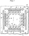
- Fig. 1 is a bottom view of the surface-mounted semiconductor package in manufacturing process according to an embodiment of this invention;
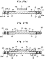
- Fig. 2 (a) is a cross sectional view of the surface-mounted semiconductor package in processing of die bonding, taken along a line II-II of Fig. 3;
- Fig. 2 (b) is a cross sectional view of the surface-mounted semiconductor package in processing of wire bonding, taken along a line II-II of Fig. 3;
- Fig. 2(c) is a cross sectional view of the surface-mounted semiconductor package in processing of molding, taken along II-II of Fig. 3;
- Fig. 3 is a top view of the surface-mounted semiconductor package of Fig. 1;
- Fig. 4 is a cross sectional view of the complete surface-mounted semiconductor package of Fig. 1;
- Fig. 5 is an enlarged cross sectional view of the boxed part indicated by symbol A of Fig. 4;
- Fig. 6 is a cross sectional view of the surface-mounted semiconductor package, taken along a line IV-IV of Fig. 7;
- Fig. 7 is a top view of the surface-mounted semiconductor package according to another embodiment of this invention;
- Fig. 8 is a cross sectional view of the complete surface-mounted semiconductor package of Fig. 7;
- Fig. 9 is an enlarged cross sectional view of the boxed part indicated by symbol A of Fig. 8;
- Fig. 10 is a cross sectional view of the conventional surface-mounted semiconductor package;
- Fig. 11(a) is an enlarged cross sectional view of the boxed part indicated by symbol A of Fig. 10; and
- Fig. 11(b) is another enlarged cross sectional view of the boxed part indicated by symbol A of Fig. 10.
- The surface-mounted
semiconductor package 10 according to the present invention is assembled in a predetermined area(equivalent to substrate 11a) on the insulating board 11, as shown in Figs. 1 and 2. As with a conventional semiconductor package, the insulating board 11, which includes many substrates 11a, is made offibers 12 such as glass fibers to be stacked and bound together with adhesives such as epoxy resin (see Fig. 5). - In every predetermined area 11a of the insulating board 11, there are many
conductive patterns 14 around a partial area of the predetermined area 11a in which thesemiconductor device 13 such as an IC chip is mounted, as shown in Fig. 2 (a). Theseconductive patterns 14 correspond to theelectrode pads 13a on thesemiconductor device 13 respectively. On the bottom of the insulating board 11, there are alsoconductive patterns 15 corresponding to theconductive patterns 14. - Each of the
conductive patterns 14 is electrically connected to its correspondingconductive pattern 15 through theconductive tube 17 made of metallic coatings, such as copper coatings, which is formed on the inside wall of the through-hole 16 going through the insulating board 11 vertically, i.e. in the direction of the thickness thereof. On eachconductive pattern 15, a ball-like terminal 18 is attached, which connects the insulating board 11 to the printedcircuit board 24 described later, and which serves as an input/output terminal of the surface-mountedsemiconductor package 10. The through-hole 16 is made by drilling through the insulating board 11 using a tool such as a drill, and theconductive tube 17 is formed by plating the inside wall of the through-hole 16. - As shown in Fig. 1 and Fig. 4, there are four
elongated slots 19 near the through-holes 16 on the insulating board 11, with their ends close each other. As with the through-holes 16, eachslot 19 is drilled through the insulating board 11 vertically, and are preferably to be made at the same time the through-holes 16 are made. The inside wall and opening edges of theslot 19 on both sides of the insulating board 11 are all coated with themetallic coating 20. Thismetallic coating 20 is composed of two continuous parts: one is thecylindrical stem 20a which covers the inside wall of theslot 19, the other is theland 20b which covers the opening edges of theslot 19 on both sides of the insulating board 11. - It is desirable that this
metallic coating 20 be formed as follows: First, thin metallic coating such as copper coating is formed on the inside wall and opening edges of theslot 19 through non-electrolytic plating. Next, masking the areas of coating corresponding to thestem 20a and thelands 20b, the other needless areas except for the above masking areas are removed by etching. The thin metallic coating on thestem 20a and on thelands 20b is developed by the electrolytic plating. The metallic coating on the inside wall of thestem 20a and on thelands 20b is completed. Thismetallic coating 20 is preferably to be made at the same time theconductive tube 17 are plated. - After a plurality of pairs of the
stem 20a and thelands 20b connected each other, are created on the insulating board 11 as well as theconductive patterns semiconductor device 13 is attached in the partial area abovementioned on the insulating board 11, that is, in the area which is surrounded by the above components, with a bonding means such as adhesives with theelectrode pads 13a being upward, as shown Fig. 2 (a). - Then, as shown in Fig. 2 (b), each
electrode pad 13a on thesemiconductor device 13 is connected to the correspondingconductive pattern 14 with thebonding wire 21. Furthermore, as shown in Fig. 2 (c), thesemiconductor device 13, thebonding wire 21, and part of theconductive patterns 14 are sealed with the sealingmaterial 22 composed of synthetic resin. Theterminals 18 which function as input/output pins of the surface-mountedsemiconductor package 10 are attached on theconductive patterns 15 on the bottom of the insulating board 11. - The
semiconductor package 10 is assembled on the insulating board 11 as described above. Then, in order to separate the surface-mountedsemiconductor package 10 from the insulating board 11, all of four corners of the substrate 11a are punched with the use of theround punch 23, as shown in Fig. 3, so that the both ends 19a of eachslot 19 are removed. Namely, anend 19a is joined to anadjacent end 19a. - Punching the corners with the use of the
punch 23 removes theends 19a of eachslot 19, causing a part 11a of the insulating board 11 which is surrounded by fourslots 19 and in which thesemiconductor device 13 andconductive patterns semiconductor package 10. The surface-mountedsemiconductor package 10 is separated from the insulating board 11 in this manner. - The surface-mounted
semiconductor package 10 is connected to thewiring areas 24a lying on the surface of the printedcircuit board 24 via theterminals 18 in conventional fashion. - As the result that the surface-mounted
semiconductor package 10 is removed from the insulating board 11, the linear peripheral edge portions, that is, the sides and the edges of the substrate 11a are covered by apart 200 of themetallic coating 20 formed on the inside wall and opening edges of eachslot 19, as shown in Fig. 4. Except for the four corners of the substrate 11a, thepart 200 of themetallic coating 20 extends along the linear peripheral edge portions of the substrate 11a. Thestem 20a covers each side of the substrate 11a, while a pair oflands 20b cover the edges on the top and bottom of the substrate 11a. The protect means 200 protects the substrate 11a in such a manner. - As shown in the enlarged diagram in Fig. 5, this protecting means 200 has the
stem 20a to cover the sides of the substrate 11a, preventing water from infiltrating the substrate 11a. In addition, protecting means 200 has a pair oflands 20b extending from thestem 20a, and secures and fastens the edges of the substrate 11a, thus preventing the edges from being peeled off and the cracks from being caused and developed. - The surface-mounted
semiconductor package 10 according to the present invention has the protecting means 200 to prevent water and other foreign matters from infiltrating the substrate 11a and, additionally prevents the edge of the substrate 11a from being peeled off and the cracks from being caused. Therefore, the protecting means 200 prevents damage to the substrate 11a and furthermore, avoids electric disconnection due to damage in theconductive tube 17 caused by peeled edges or cracks in the substrate 11a, increasing the durability of the surface-mountedsemiconductor package 10. - Figs. 6 to 9 show the surface-mounted
semiconductor package 110 used in another embodiment of the present invention. The same reference symbols are used for the components of the surface-mountedsemiconductor package 110 that are functionally equivalent to those in the surface-mountedsemiconductor package 10 shown in Figs. 1 to 5. - In the surface-mounted
semiconductor package 110, themetallic cover 25 is used instead of the sealingmaterial 22 in use for the surface-mountedsemiconductor package 10. Thelands 20b of themetallic coating 20 , which are on the openings of theslot 19, are placed on the top and bottom of the insulating board 11, as shown in Fig. 9. - As shown in Fig. 6, the
conductive patterns conductive tubes 17 each connecting thecorresponding conducting patterns slots 19, and themetallic coatings 20 are formed on the insulating board 11 of the surface-mountedsemiconductor package 110 as in the previous embodiment shown in Fig. 2(c). Then, theelectrode pads 13a on thesemiconductor device 13 are connected to the correspondingconductive patterns 14 via thebonding wires 21. Finally, themetallic cover 25 is mounted on the insulating board 11 to cover thesemiconductor device 13,bonding wires 21, andconductive patterns 14. - The
metallic cover 25 is composed of the flat, rectangle top 25a which covers the substrate 11a, and thesides 25b which extend downward from the four sides of the top 25a. Except for the four corners of themetallic cover 25, the bottom edges of thesides 25b are inserted into theslots 19. With its sides being inserted into theslots 19, themetallic cover 25 is fastened to thelands 20b on the top of the board 11, for example, by soldering. - A cover of some other materials such as synthetic resin may be used in stead of the
metallic cover 25. In that case, however, the bonding means such as synthetic resin, is required to fasten the cover. On the contrary, themetallic cover 25 may be fixed to themetallic lands 20b by applying solder which is more powerful than any other bonding material made of synthetic resin, which enables the fastening of themetallic cover 25 to be more stiff or rigid. - After mounting the
metallic cover 25, theterminals 18 are attached to theconductive patterns 15 on the bottom of the insulating board 11. Then, as shown in Fig. 7, theends 19a of eachslot 19 on the insulating board 11 are punched with thepunch 23 to remove the four corners of the substrate 11a. As shown in Fig. 7, the L-shapedpunch 23 is used to punch the area of the insulating board 11 not covered by themetallic cover 25. - Punching the insulating board 11 with the use of the
punch 23, which is shown in Fig. 8, separates from the insulating board 11 a part 11a of the insulating board 11 where thesemiconductor device 13 andconductive patterns 14 are mounted. The separated part is the substrate 11a of the surface-mountedsemiconductor package 110. The surface-mountedsemiconductor package 110 is separated from the insulating board 11 in this manner. - As with the surface-mounted
semiconductor package 10, apart 200 of themetallic coating 20 with thestem 20a and thelands 20b, which was originally formed as the inside wall and opening edges of theslot 19 is used as the protecting means. That is, the surface-mountedsemiconductor package 110 has thestems 20a to cover the sides of the substrate 11a and the pairs oflands 20b to cover the edges on the top and bottom of the substrate 11a. Accordingly, the surface-mountedsemiconductor package 110 obtains the same protection as that of the surface-mountedsemiconductor package 10. - In order to separate the substrate 11a from the insulating board 11, various types of cutting means may be used instead of punching the insulating board 11 to remove or join the
ends 19a of eachslot 19. - In the above discussion, the embodiments in which the present invention is applied to a BGA-type package, where ball-like terminals are used. The present invention may be applied not only to this type of package but also to various types of surface-mounted semiconductor package with a multiple layers such as a PGA (Pin Grid Array), where pin-shaped terminals are used as the
terminals 18.
Claims (10)
- A surface-mounted semiconductor package mounted on the top of a printed circuit board comprising:an insulating substrate with a stack structure;a semiconductor device mounted on the top of the insulating substrate and having a plurality of electrode pads;a plurality of input/output terminals mounted on the bottom of the insulating substrate for attaching the semiconductor package to the printed circuit board;a plurality of conductive portions penetrating the insulating substrate in the direction of the thickness thereof for electrically connecting the input/output terminals to the electrode pads respectively; andprotecting means covering the sides of the insulating substrate and having a plurality of pairs of lands along the edges of the top and bottom of the insulating substrate.
- A surface-mounted semiconductor package as set forth in claim 1, wherein the insulating substrate is shaped like a rectangle and the protecting means is provided along the linear peripheral portions of the insulating substrate except for the four corners.
- A surface-mounted semiconductor package as set forth in claim 1, wherein the protecting means is composed of metallic coating.
- A surface-mounted semiconductor package as set forth in claim 3, further comprising a metallic cover covering the semiconductor device, the metallic cover being fastened to the protecting means.
- A method for manufacturing a surface-mounted semiconductor package with a semiconductor device, mounted on the top of a printed circuit board, the method comprising the steps of:making a plurality of elongated slots through a stack-structured insulating board, the slots being spaced each other so as to surround the semiconductor device cooperatively;forming a metallic coating on the inside walls of each of the slots and on the opening edges of each of the slots on both top and bottom of the insulating board; andjoining the ends of each of the slots each other to separate an area surrounded by the slots from the insulating board for use as the substrate.
- A method for manufacturing a surface-mounted semiconductor package as set forth in claim 5, wherein the substrate is separated from the insulating board by punching the ends of the slots adjacent to each other.
- A method for manufacturing a surface-mounted semiconductor package as set forth in claim 5, wherein the step of forming the metallic coating comprises the steps of:forming a thin metallic coating on the peripheral edge portions of the insulating board through non-electrolytic plating;patterning the thin metallic coating into a desired shape; anddeveloping remaining patterned part of the thin metallic coating through electrolytic plating to obtain a desired thickness thereof.
- A method for manufacturing a surface-mounted semiconductor package as set forth in claim 7, wherein the surface-mounted semiconductor package has conductive portions which is composed of metallic coating and is formed on the inside wall of a through-hole going through the substrate from the top to the bottom, wherein the step of forming a metallic coating on the inside walls and opening edges of the slots and the step of forming are performed simultaneously.
- A method for manufacturing a surface-mounted semiconductor package as set forth in claim 5 further comprising the step of sealing the semiconductor device with resin, wherein the step of joining is performed after the step of sealing.
- A method for manufacturing a surface-mounted semiconductor package as set forth in claim 5 further comprising the step of sealing the semiconductor with a metallic cover, wherein the step of joining is performed after the step of sealing.
Applications Claiming Priority (2)
| Application Number | Priority Date | Filing Date | Title |
|---|---|---|---|
| JP324138/95 | 1995-12-13 | ||
| JP32413895A JP3432982B2 (en) | 1995-12-13 | 1995-12-13 | Method for manufacturing surface mount semiconductor device |
Publications (2)
| Publication Number | Publication Date |
|---|---|
| EP0779657A2 true EP0779657A2 (en) | 1997-06-18 |
| EP0779657A3 EP0779657A3 (en) | 1998-11-11 |
Family
ID=18162566
Family Applications (1)
| Application Number | Title | Priority Date | Filing Date |
|---|---|---|---|
| EP96118894A Withdrawn EP0779657A3 (en) | 1995-12-13 | 1996-11-25 | Surface-mounted semiconductor package and its manufacturing method |
Country Status (5)
| Country | Link |
|---|---|
| US (1) | US5886876A (en) |
| EP (1) | EP0779657A3 (en) |
| JP (1) | JP3432982B2 (en) |
| KR (1) | KR970058407A (en) |
| TW (1) | TW341722B (en) |
Families Citing this family (79)
| Publication number | Priority date | Publication date | Assignee | Title |
|---|---|---|---|---|
| JP3076527B2 (en) | 1997-02-14 | 2000-08-14 | 株式会社イースタン | Wiring board |
| JP3173410B2 (en) * | 1997-03-14 | 2001-06-04 | 松下電器産業株式会社 | Package substrate and method of manufacturing the same |
| EP1035586A4 (en) * | 1997-10-20 | 2007-01-24 | Hitachi Ltd | Semiconductor module and power converter comprising it |
| US5969947A (en) | 1997-12-17 | 1999-10-19 | International Business Machines Corporation | Integral design features for heatsink attach for electronic packages |
| SG73490A1 (en) * | 1998-01-23 | 2000-06-20 | Texas Instr Singapore Pte Ltd | High density internal ball grid array integrated circuit package |
| US6300679B1 (en) * | 1998-06-01 | 2001-10-09 | Semiconductor Components Industries, Llc | Flexible substrate for packaging a semiconductor component |
| TW388976B (en) * | 1998-10-21 | 2000-05-01 | Siliconware Precision Industries Co Ltd | Semiconductor package with fully exposed heat sink |
| JP3179420B2 (en) * | 1998-11-10 | 2001-06-25 | 日本電気株式会社 | Semiconductor device |
| WO2000042636A2 (en) * | 1999-01-12 | 2000-07-20 | Teledyne Technologies Incorporated | Micromachined device and method of forming the micromachined device |
| JP3437477B2 (en) * | 1999-02-10 | 2003-08-18 | シャープ株式会社 | Wiring board and semiconductor device |
| EP1030366B1 (en) | 1999-02-15 | 2005-10-19 | Mitsubishi Gas Chemical Company, Inc. | Printed wiring board for semiconductor plastic package |
| US6282100B1 (en) * | 1999-07-01 | 2001-08-28 | Agere Systems Guardian Corp. | Low cost ball grid array package |
| US6359233B1 (en) * | 1999-10-26 | 2002-03-19 | Intel Corporation | Printed circuit board multipack structure having internal gold fingers and multipack and printed circuit board formed therefrom, and methods of manufacture thereof |
| US20020003049A1 (en) * | 1999-12-29 | 2002-01-10 | Sanjay Dabral | Inline and "Y" input-output bus topology |
| US7434305B2 (en) | 2000-11-28 | 2008-10-14 | Knowles Electronics, Llc. | Method of manufacturing a microphone |
| US8623709B1 (en) | 2000-11-28 | 2014-01-07 | Knowles Electronics, Llc | Methods of manufacture of top port surface mount silicon condenser microphone packages |
| US6515222B2 (en) * | 2001-02-05 | 2003-02-04 | Motorola, Inc. | Printed circuit board arrangement |
| DE10142971A1 (en) * | 2001-09-01 | 2003-03-27 | Eupec Gmbh & Co Kg | The power semiconductor module |
| US6803527B2 (en) * | 2002-03-26 | 2004-10-12 | Intel Corporation | Circuit board with via through surface mount device contact |
| TW565009U (en) * | 2003-01-20 | 2003-12-01 | Benq Corp | Electronic module having ball grid array |
| US7042098B2 (en) * | 2003-07-07 | 2006-05-09 | Freescale Semiconductor,Inc | Bonding pad for a packaged integrated circuit |
| DE102005008512B4 (en) | 2005-02-24 | 2016-06-23 | Epcos Ag | Electrical module with a MEMS microphone |
| DE102005008511B4 (en) * | 2005-02-24 | 2019-09-12 | Tdk Corporation | MEMS microphone |
| DE102005008514B4 (en) * | 2005-02-24 | 2019-05-16 | Tdk Corporation | Microphone membrane and microphone with the microphone membrane |
| JP4614818B2 (en) * | 2005-05-09 | 2011-01-19 | パナソニック株式会社 | Semiconductor device and manufacturing method thereof |
| DE102005053765B4 (en) * | 2005-11-10 | 2016-04-14 | Epcos Ag | MEMS package and method of manufacture |
| DE102005053767B4 (en) * | 2005-11-10 | 2014-10-30 | Epcos Ag | MEMS microphone, method of manufacture and method of installation |
| JP4770514B2 (en) * | 2006-02-27 | 2011-09-14 | 株式会社デンソー | Electronic equipment |
| KR100808644B1 (en) * | 2006-06-09 | 2008-02-29 | 주식회사 이츠웰 | Lamp having surface mounted light emitting diode and manufacturing method of the same |
| TWI339881B (en) * | 2007-02-15 | 2011-04-01 | Via Tech Inc | Chip package |
| TW200908819A (en) * | 2007-06-15 | 2009-02-16 | Ngk Spark Plug Co | Wiring substrate with reinforcing member |
| US20090026599A1 (en) * | 2007-07-27 | 2009-01-29 | Powertech Technology Inc. | Memory module capable of lessening shock stress |
| EP2178353B1 (en) * | 2007-08-09 | 2012-02-29 | Panasonic Corporation | Circuit module, and electronic device using the module |
| CN101471307B (en) * | 2007-12-29 | 2012-07-04 | 三星电子株式会社 | Semiconductor encapsulation body and manufacturing method thereof |
| US8350367B2 (en) * | 2008-02-05 | 2013-01-08 | Advanced Semiconductor Engineering, Inc. | Semiconductor device packages with electromagnetic interference shielding |
| US8212339B2 (en) | 2008-02-05 | 2012-07-03 | Advanced Semiconductor Engineering, Inc. | Semiconductor device packages with electromagnetic interference shielding |
| US7989928B2 (en) | 2008-02-05 | 2011-08-02 | Advanced Semiconductor Engineering Inc. | Semiconductor device packages with electromagnetic interference shielding |
| US8022511B2 (en) * | 2008-02-05 | 2011-09-20 | Advanced Semiconductor Engineering, Inc. | Semiconductor device packages with electromagnetic interference shielding |
| CN101960588A (en) * | 2008-03-14 | 2011-01-26 | 松下电器产业株式会社 | Semiconductor device and semiconductor device fabrication method |
| JP2010004011A (en) * | 2008-05-19 | 2010-01-07 | Panasonic Corp | Semiconductor device and fabrication method thereof |
| JP5320863B2 (en) * | 2008-07-02 | 2013-10-23 | オムロン株式会社 | Electronic components |
| US7829981B2 (en) * | 2008-07-21 | 2010-11-09 | Advanced Semiconductor Engineering, Inc. | Semiconductor device packages with electromagnetic interference shielding |
| US8410584B2 (en) * | 2008-08-08 | 2013-04-02 | Advanced Semiconductor Engineering, Inc. | Semiconductor device packages with electromagnetic interference shielding |
| JP5298714B2 (en) * | 2008-09-05 | 2013-09-25 | 富士通セミコンダクター株式会社 | Manufacturing method of semiconductor device |
| US20100110656A1 (en) | 2008-10-31 | 2010-05-06 | Advanced Semiconductor Engineering, Inc. | Chip package and manufacturing method thereof |
| US20100207257A1 (en) * | 2009-02-17 | 2010-08-19 | Advanced Semiconductor Engineering, Inc. | Semiconductor package and manufacturing method thereof |
| US8110902B2 (en) * | 2009-02-19 | 2012-02-07 | Advanced Semiconductor Engineering, Inc. | Chip package and manufacturing method thereof |
| US8212340B2 (en) | 2009-07-13 | 2012-07-03 | Advanced Semiconductor Engineering, Inc. | Chip package and manufacturing method thereof |
| US8207455B2 (en) * | 2009-07-31 | 2012-06-26 | Power Integrations, Inc. | Power semiconductor package with bottom surface protrusions |
| US8368185B2 (en) * | 2009-11-19 | 2013-02-05 | Advanced Semiconductor Engineering, Inc. | Semiconductor device packages with electromagnetic interference shielding |
| US8378466B2 (en) * | 2009-11-19 | 2013-02-19 | Advanced Semiconductor Engineering, Inc. | Wafer-level semiconductor device packages with electromagnetic interference shielding |
| US8030750B2 (en) * | 2009-11-19 | 2011-10-04 | Advanced Semiconductor Engineering, Inc. | Semiconductor device packages with electromagnetic interference shielding |
| TWI497679B (en) * | 2009-11-27 | 2015-08-21 | Advanced Semiconductor Eng | Semiconductor package and manufacturing method thereof |
| US8569894B2 (en) | 2010-01-13 | 2013-10-29 | Advanced Semiconductor Engineering, Inc. | Semiconductor package with single sided substrate design and manufacturing methods thereof |
| TWI411075B (en) | 2010-03-22 | 2013-10-01 | Advanced Semiconductor Eng | Semiconductor package and manufacturing method thereof |
| US9362196B2 (en) * | 2010-07-15 | 2016-06-07 | Kabushiki Kaisha Toshiba | Semiconductor package and mobile device using the same |
| TWI540698B (en) | 2010-08-02 | 2016-07-01 | 日月光半導體製造股份有限公司 | Semiconductor package and manufacturing method thereof |
| US9007273B2 (en) | 2010-09-09 | 2015-04-14 | Advances Semiconductor Engineering, Inc. | Semiconductor package integrated with conformal shield and antenna |
| US9406658B2 (en) | 2010-12-17 | 2016-08-02 | Advanced Semiconductor Engineering, Inc. | Embedded component device and manufacturing methods thereof |
| CN103999484B (en) | 2011-11-04 | 2017-06-30 | 美商楼氏电子有限公司 | As the embedded-type electric medium and manufacture method of the barrier in acoustic equipment |
| US8541883B2 (en) | 2011-11-29 | 2013-09-24 | Advanced Semiconductor Engineering, Inc. | Semiconductor device having shielded conductive vias |
| US8937376B2 (en) | 2012-04-16 | 2015-01-20 | Advanced Semiconductor Engineering, Inc. | Semiconductor packages with heat dissipation structures and related methods |
| US8786060B2 (en) | 2012-05-04 | 2014-07-22 | Advanced Semiconductor Engineering, Inc. | Semiconductor package integrated with conformal shield and antenna |
| US8704341B2 (en) | 2012-05-15 | 2014-04-22 | Advanced Semiconductor Engineering, Inc. | Semiconductor packages with thermal dissipation structures and EMI shielding |
| US8653634B2 (en) | 2012-06-11 | 2014-02-18 | Advanced Semiconductor Engineering, Inc. | EMI-shielded semiconductor devices and methods of making |
| US9153542B2 (en) | 2012-08-01 | 2015-10-06 | Advanced Semiconductor Engineering, Inc. | Semiconductor package having an antenna and manufacturing method thereof |
| US9078063B2 (en) | 2012-08-10 | 2015-07-07 | Knowles Electronics, Llc | Microphone assembly with barrier to prevent contaminant infiltration |
| JP2014072220A (en) | 2012-09-27 | 2014-04-21 | International Business Maschines Corporation | Method of manufacturing printed circuit board |
| CN103096631B (en) * | 2013-01-08 | 2016-01-20 | 广东生益科技股份有限公司 | A kind of PCB processing method and pcb board |
| US9978688B2 (en) | 2013-02-28 | 2018-05-22 | Advanced Semiconductor Engineering, Inc. | Semiconductor package having a waveguide antenna and manufacturing method thereof |
| US9837701B2 (en) | 2013-03-04 | 2017-12-05 | Advanced Semiconductor Engineering, Inc. | Semiconductor package including antenna substrate and manufacturing method thereof |
| US9129954B2 (en) | 2013-03-07 | 2015-09-08 | Advanced Semiconductor Engineering, Inc. | Semiconductor package including antenna layer and manufacturing method thereof |
| US9172131B2 (en) | 2013-03-15 | 2015-10-27 | Advanced Semiconductor Engineering, Inc. | Semiconductor structure having aperture antenna |
| DE102013106353B4 (en) * | 2013-06-18 | 2018-06-28 | Tdk Corporation | Method for applying a structured coating to a component |
| CN103400825B (en) | 2013-07-31 | 2016-05-18 | 日月光半导体制造股份有限公司 | Semiconductor package part and manufacture method thereof |
| JP2015115558A (en) * | 2013-12-13 | 2015-06-22 | 株式会社東芝 | Semiconductor device |
| DE112015002947A5 (en) * | 2014-06-23 | 2017-03-16 | Epcos Ag | Housing for an electrical component and method for producing a housing for an electrical component |
| US9794661B2 (en) | 2015-08-07 | 2017-10-17 | Knowles Electronics, Llc | Ingress protection for reducing particle infiltration into acoustic chamber of a MEMS microphone package |
| JP6809600B2 (en) * | 2017-04-03 | 2021-01-06 | 株式会社村田製作所 | High frequency module |
Family Cites Families (21)
| Publication number | Priority date | Publication date | Assignee | Title |
|---|---|---|---|---|
| US3735211A (en) * | 1971-06-21 | 1973-05-22 | Fairchild Camera Instr Co | Semiconductor package containing a dual epoxy and metal seal between a cover and a substrate, and method for forming said seal |
| JPS51111276A (en) * | 1975-03-26 | 1976-10-01 | Nippon Sheet Glass Co Ltd | Molded article of polycarbonate resin of improved abrasion resistance |
| US4251852A (en) * | 1979-06-18 | 1981-02-17 | International Business Machines Corporation | Integrated circuit package |
| JPS5879706A (en) * | 1981-11-06 | 1983-05-13 | Matsushita Electric Ind Co Ltd | Chip inductor |
| JPS59152650A (en) * | 1983-02-21 | 1984-08-31 | Mitsubishi Electric Corp | Semiconductor device |
| US4819041A (en) * | 1983-12-30 | 1989-04-04 | Amp Incorporated | Surface mounted integrated circuit chip package and method for making same |
| JPS60226142A (en) * | 1984-04-25 | 1985-11-11 | Hitachi Ltd | Module structure |
| JPS6124253A (en) * | 1984-07-13 | 1986-02-01 | Hitachi Ltd | Structure for semiconductor package |
| US4707565A (en) * | 1985-03-19 | 1987-11-17 | Nitto Boseki Co., Ltd. | Substrate for printed circuit |
| JPS62204550A (en) * | 1986-03-05 | 1987-09-09 | Shinko Electric Ind Co Ltd | Printed substrate type semiconductor package |
| JPS62274753A (en) * | 1986-05-23 | 1987-11-28 | Seiko Instr & Electronics Ltd | Structure of pin grid array package |
| JP2550991B2 (en) * | 1987-05-06 | 1996-11-06 | 日本電気株式会社 | Pin grid array semiconductor module |
| JPH01135099A (en) * | 1987-11-20 | 1989-05-26 | Ibiden Co Ltd | Electronic circuit package |
| FI85794C (en) * | 1989-07-05 | 1992-05-25 | Nokia Mobira Oy | FOERFARANDE FOER ATT SKYDDA ETT KRETSKORT ELLER EN DEL DAERAV MOT STOERNINGAR SOM ALSTRATS AV ELEKTROMAGNETISK INTERFERENS, OCH SKYDDSHOELJE FOER ANVAENDNING I FOERFARANDET. |
| US5031025A (en) * | 1990-02-20 | 1991-07-09 | Unisys Corporation | Hermetic single chip integrated circuit package |
| US5060844A (en) * | 1990-07-18 | 1991-10-29 | International Business Machines Corporation | Interconnection structure and test method |
| US5153379A (en) * | 1990-10-09 | 1992-10-06 | Motorola, Inc. | Shielded low-profile electronic component assembly |
| CA2089435C (en) * | 1992-02-14 | 1997-12-09 | Kenzi Kobayashi | Semiconductor device |
| EP0582881B1 (en) * | 1992-07-27 | 1997-12-29 | Murata Manufacturing Co., Ltd. | Multilayer electronic component, method of manufacturing the same and method of measuring characteristics thereof |
| US5686172A (en) * | 1994-11-30 | 1997-11-11 | Mitsubishi Gas Chemical Company, Inc. | Metal-foil-clad composite ceramic board and process for the production thereof |
| US5642262A (en) * | 1995-02-23 | 1997-06-24 | Altera Corporation | High-density programmable logic device in a multi-chip module package with improved interconnect scheme |
-
1995
- 1995-12-13 JP JP32413895A patent/JP3432982B2/en not_active Expired - Fee Related
-
1996
- 1996-11-11 KR KR1019960053244A patent/KR970058407A/en not_active Application Discontinuation
- 1996-11-11 TW TW085113750A patent/TW341722B/en active
- 1996-11-25 EP EP96118894A patent/EP0779657A3/en not_active Withdrawn
- 1996-12-05 US US08/760,473 patent/US5886876A/en not_active Expired - Fee Related
Non-Patent Citations (1)
| Title |
|---|
| None |
Also Published As
| Publication number | Publication date |
|---|---|
| TW341722B (en) | 1998-10-01 |
| KR970058407A (en) | 1997-07-31 |
| JP3432982B2 (en) | 2003-08-04 |
| US5886876A (en) | 1999-03-23 |
| JPH09162322A (en) | 1997-06-20 |
| EP0779657A3 (en) | 1998-11-11 |
Similar Documents
| Publication | Publication Date | Title |
|---|---|---|
| US5886876A (en) | Surface-mounted semiconductor package and its manufacturing method | |
| US6012224A (en) | Method of forming compliant microelectronic mounting device | |
| USRE36773E (en) | Method for plating using nested plating buses and semiconductor device having the same | |
| US5789811A (en) | Surface mount peripheral leaded and ball grid array package | |
| US6256877B1 (en) | Method for transforming a substrate with edge contacts into a ball grid array | |
| US7615872B2 (en) | Semiconductor device | |
| US5177863A (en) | Method of forming integrated leadouts for a chip carrier | |
| EP1168447A2 (en) | Multi-layered semiconductor device and method | |
| EP0536418A1 (en) | Semiconductor device and manufacturing method therefor | |
| US5357400A (en) | Tape automated bonding semiconductor device and production process thereof | |
| US20010042924A1 (en) | Semiconductor package | |
| EP0843357B1 (en) | Method of manufacturing a grid array semiconductor package | |
| EP0814510B1 (en) | TAB tape and semiconductor device using the TAB tape | |
| US20070096271A1 (en) | Substrate frame | |
| US6121678A (en) | Wrap-around interconnect for fine pitch ball grid array | |
| EP1436838A2 (en) | Semiconductor component | |
| KR100271676B1 (en) | Package and semiconductor device for semiconductor device and their manufacturing method | |
| KR100250560B1 (en) | Semiconductor device and its manufacture | |
| US6444494B1 (en) | Process of packaging a semiconductor device with reinforced film substrate | |
| EP1154479A2 (en) | Multiple line grid for use in a packaging or a testing application | |
| JPH0517709B2 (en) | ||
| JPH10154768A (en) | Semiconductor device and its manufacturing method | |
| US20230063343A1 (en) | Multilevel package substrate device with bga pin out and coaxial signal connections | |
| KR100243023B1 (en) | Semiconductor package and method of manufacturing and laminating it | |
| KR100246848B1 (en) | Land grid array and a semiconductor package having a same |
Legal Events
| Date | Code | Title | Description |
|---|---|---|---|
| PUAI | Public reference made under article 153(3) epc to a published international application that has entered the european phase |
Free format text: ORIGINAL CODE: 0009012 |
|
| AK | Designated contracting states |
Kind code of ref document: A2 Designated state(s): DE FR GB NL |
|
| PUAL | Search report despatched |
Free format text: ORIGINAL CODE: 0009013 |
|
| AK | Designated contracting states |
Kind code of ref document: A3 Designated state(s): DE FR GB NL |
|
| STAA | Information on the status of an ep patent application or granted ep patent |
Free format text: STATUS: THE APPLICATION IS DEEMED TO BE WITHDRAWN |
|
| 18D | Application deemed to be withdrawn |
Effective date: 19990708 |