EP0785620A2 - Surface acoustic wave device - Google Patents
Surface acoustic wave device Download PDFInfo
- Publication number
- EP0785620A2 EP0785620A2 EP97100637A EP97100637A EP0785620A2 EP 0785620 A2 EP0785620 A2 EP 0785620A2 EP 97100637 A EP97100637 A EP 97100637A EP 97100637 A EP97100637 A EP 97100637A EP 0785620 A2 EP0785620 A2 EP 0785620A2
- Authority
- EP
- European Patent Office
- Prior art keywords
- piezoelectric substrate
- thin film
- electrode pattern
- interdigital electrode
- resistor thin
- Prior art date
- Legal status (The legal status is an assumption and is not a legal conclusion. Google has not performed a legal analysis and makes no representation as to the accuracy of the status listed.)
- Withdrawn
Links
Images

Classifications
-
- H—ELECTRICITY
- H03—ELECTRONIC CIRCUITRY
- H03H—IMPEDANCE NETWORKS, e.g. RESONANT CIRCUITS; RESONATORS
- H03H9/00—Networks comprising electromechanical or electro-acoustic devices; Electromechanical resonators
- H03H9/02—Details
- H03H9/02535—Details of surface acoustic wave devices
- H03H9/02818—Means for compensation or elimination of undesirable effects
- H03H9/02921—Measures for preventing electric discharge due to pyroelectricity
Definitions
- the present invention relates to a surface acoustic wave (SAW) device and, more particularly to an SAW device in which noise caused by the pyroelectric effect of the piezoelectric substrate is suppressed.
- SAW surface acoustic wave
- an SAW device such as an SAW filter has appropriately weighted interdigital transducers (IDTs) as input/output transducers on the surface of the piezoelectric substrate to perform conversion between an electrical signal and an SAW.
- IDTs interdigital transducers
- an IDT pattern is merely formed of a conductive thin film on the piezoelectric substrate.
- Fig. 3A shows an example of a conventional SAW device
- Fig. 3B shows the device of Fig. 3A along the line B - B'.
- the conventional SAW device merely the pattern of IDTs 22 and 22' is directly formed of a conductive thin film on a piezoelectric substrate 21.
- the charges on the surface of the piezoelectric substrate 21 are not discharged unless they become equal to or more than the dielectric breakdown of the surrounding atmosphere of the piezoelectric substrate 21.
- the amount of charges removed at once becomes large to increase the noise level.
- the piezoelectric substrate 21 has a strong pyroelectric effect, and the above drawback is remarkable.
- a surface acoustic wave device comprising a piezoelectric substrate having a piezoelectric effect, an interdigital electrode pattern made of a conductive thin film and formed on the piezoelectric substrate to perform conversion between an electrical signal and a surface acoustic wave, and a resistor thin film formed on the piezoelectric substrate to electrically connect the piezoelectric substrate to the interdigital electrode pattern, the resistor thin film serving to remove charges from a surface of the piezoelectric substrate due to a pyroelectric effect to the interdigital electrode pattern.
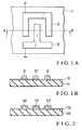
- Fig. 1A shows a surface acoustic wave (SAW) device according to the first embodiment of the present invention
- Fig. 1B shows the surface acoustic wave device of Fig. 1A along the line A - A'.
- SAW surface acoustic wave
- a resistor thin film 13 having a low resistance is formed on the entire surface of a piezoelectric substrate 11, and a pattern of IDTs 12 and 12' made of a conductive film, e.g., aluminum, is formed on the resistor thin film 13 to have a predetermined shape. Discharge can be facilitated when the resistance of the resistor thin film is minimized within the range which does not adversely affect the electrical performance of the SAW filter.
- the material of the piezoelectric substrate 11 e.g., lithium tantalate (LiTaO 3 ) or lithium niobate (LiNbO 3 ) is used.
- the resistor thin film 13 e.g., a silicon (Si) thin film formed by sputtering or vapor deposition is used.
- the SAW device When the SAW device functions as an input transducer, upon application of an RF electrical signal across the IDTs 12 and 12', an RF electric field is generated, and an SAW is excited by the piezoelectric effect of the piezoelectric substrate 11.
- the SAW device When the SAW device functions as an output transducer, upon reception of an SAW, an RF electric field is generated by the piezoelectric reaction to output an electrical signal between the IDTs 12 and 12'.
- the high-resistance resistor thin film 13 interposed between the IDTs 12 and 12' and the piezoelectric substrate 11 constitutes a discharge line for the charges of the piezoelectric substrate 11. Therefore, the charges generated on the surface of the piezoelectric substrate 11 upon a change in ambient temperature due to the pyroelectric effect of the piezoelectric substrate 11 are removed to the IDTs 12 and 12' through the resistor thin film 13 as soon as they are generated. In other words, the charges are not accumulated on the surface of the piezoelectric substrate 11.
- the charges generated on the surface of the piezoelectric substrate 11 are removed to the IDTs 12 and 12' as soon as they are generated, the amount of removed charges is very small. As a result, the level of noise appearing at the input/output terminals of the SAW device can be minimized.
- Fig. 2 shows the arrangement of the second embodiment of the present invention.
- the pattern of IDTs 112 and 112' made of a conductive thin film is directly formed on the surface of a piezoelectric substrate 111, and a resistor thin film 113 is formed to cover the pattern of the IDTs 112 and 112' and the surface of the piezoelectric substrate 111.
- the contact area of the resistor thin film 113 that constitutes the discharge line and the IDTs 112 and 112' can be increased.
- the first and second embodiments may be combined. More specifically, another resistor thin film may be formed on the pattern of the IDTs 12 and 12' and the resistor thin film 13 of Fig. 1B.
- the piezoelectric substrate and the IDTs made of the conductive thin film are electrically connected to each other through the resistor thin film to constitute a discharge line for the charges from the piezoelectric substrate to the IDTs, so that the level of noise caused by the pyroelectric effect of the piezoelectric substrate and appearing at the input/output terminals of the SAW device can be suppressed and decreased.
Landscapes
- Physics & Mathematics (AREA)
- Acoustics & Sound (AREA)
- Surface Acoustic Wave Elements And Circuit Networks Thereof (AREA)
Abstract
Description
- The present invention relates to a surface acoustic wave (SAW) device and, more particularly to an SAW device in which noise caused by the pyroelectric effect of the piezoelectric substrate is suppressed.
- In general, an SAW device such as an SAW filter has appropriately weighted interdigital transducers (IDTs) as input/output transducers on the surface of the piezoelectric substrate to perform conversion between an electrical signal and an SAW. In the conventional SAW device, an IDT pattern is merely formed of a conductive thin film on the piezoelectric substrate.
- Fig. 3A shows an example of a conventional SAW device, and Fig. 3B shows the device of Fig. 3A along the line B - B'. As shown in Figs. 3A and 3B, in the conventional SAW device, merely the pattern of
IDTs 22 and 22' is directly formed of a conductive thin film on apiezoelectric substrate 21. - In the conventional SAW device shown in Figs. 3A and 3B, when the ambient temperature changes, the surface of the
piezoelectric substrate 21 is charged due to the pyroelectric effect of thepiezoelectric substrate 21. When an electric field formed by the charges becomes equal to or more than the dielectric breakdown of the surrounding atmosphere of thepiezoelectric substrate 21, the charges on thepiezoelectric substrate 21 are discharged to theIDTs 22 and 22'. - If the charges are discharged to the ground-side IDT 22', the problem of noise does not occur in the SAW device. However, if the charges are discharged to the hot-
side IDT 22, noise occurs in the SAW device. - In the latter case, the charges on the surface of the
piezoelectric substrate 21 are not discharged unless they become equal to or more than the dielectric breakdown of the surrounding atmosphere of thepiezoelectric substrate 21. Thus, the amount of charges removed at once becomes large to increase the noise level. - In particular, in an SAW device that uses lithium tantalate (LiTaO3) or lithium niobate (LiNbO3) as the material of the
piezoelectric substrate 21, thepiezoelectric substrate 21 has a strong pyroelectric effect, and the above drawback is remarkable. - It is an object of the present invention to provide a surface acoustic wave device in which generation of noise due to the pyroelectric effect of the piezoelectric substrate is suppressed.
- In order to achieve the above object, according to the present invention, there is provided a surface acoustic wave device comprising a piezoelectric substrate having a piezoelectric effect, an interdigital electrode pattern made of a conductive thin film and formed on the piezoelectric substrate to perform conversion between an electrical signal and a surface acoustic wave, and a resistor thin film formed on the piezoelectric substrate to electrically connect the piezoelectric substrate to the interdigital electrode pattern, the resistor thin film serving to remove charges from a surface of the piezoelectric substrate due to a pyroelectric effect to the interdigital electrode pattern.
-
- Fig. 1A is a plan view showing a surface acoustic wave device according to the first embodiment of the present invention, and Fig. 1B is a sectional view taken along the line A - A' of Fig. 1A;
- Fig. 2 is a sectional view showing a surface acoustic wave device according to the second embodiment of the present invention; and
- Fig. 3A is a plan view of a conventional surface acoustic wave device, and Fig. 3B is a sectional view taken along the line B - B' of Fig. 3B.
- The present invention will be described in detail with reference to the accompanying drawings.
- Fig. 1A shows a surface acoustic wave (SAW) device according to the first embodiment of the present invention, and Fig. 1B shows the surface acoustic wave device of Fig. 1A along the line A - A'.
- In the SAW device shown in Figs. 1A and 1B, a resistor
thin film 13 having a low resistance is formed on the entire surface of apiezoelectric substrate 11, and a pattern ofIDTs 12 and 12' made of a conductive film, e.g., aluminum, is formed on the resistorthin film 13 to have a predetermined shape. Discharge can be facilitated when the resistance of the resistor thin film is minimized within the range which does not adversely affect the electrical performance of the SAW filter. As the material of thepiezoelectric substrate 11, e.g., lithium tantalate (LiTaO3) or lithium niobate (LiNbO3) is used. As the resistorthin film 13, e.g., a silicon (Si) thin film formed by sputtering or vapor deposition is used. - The operation of the SAW device having the above arrangement will be described. When the SAW device functions as an input transducer, upon application of an RF electrical signal across the
IDTs 12 and 12', an RF electric field is generated, and an SAW is excited by the piezoelectric effect of thepiezoelectric substrate 11. When the SAW device functions as an output transducer, upon reception of an SAW, an RF electric field is generated by the piezoelectric reaction to output an electrical signal between theIDTs 12 and 12'. - The high-resistance resistor
thin film 13 interposed between theIDTs 12 and 12' and thepiezoelectric substrate 11 constitutes a discharge line for the charges of thepiezoelectric substrate 11. Therefore, the charges generated on the surface of thepiezoelectric substrate 11 upon a change in ambient temperature due to the pyroelectric effect of thepiezoelectric substrate 11 are removed to theIDTs 12 and 12' through the resistorthin film 13 as soon as they are generated. In other words, the charges are not accumulated on the surface of thepiezoelectric substrate 11. - Even if the charges generated on the surface of the
piezoelectric substrate 11 due to the pyroelectric effect are removed to the ground-side IDT 12', no problem occurs in the SAW device. On the contrary, if the charges are removed to the hot-side IDT 12, they appear as noise at the input/output terminals of the SAW device. - However, since the charges generated on the surface of the
piezoelectric substrate 11 are removed to theIDTs 12 and 12' as soon as they are generated, the amount of removed charges is very small. As a result, the level of noise appearing at the input/output terminals of the SAW device can be minimized. - Fig. 2 shows the arrangement of the second embodiment of the present invention.
- Referring to Fig. 2, the pattern of
IDTs 112 and 112' made of a conductive thin film is directly formed on the surface of apiezoelectric substrate 111, and a resistorthin film 113 is formed to cover the pattern of theIDTs 112 and 112' and the surface of thepiezoelectric substrate 111. In this embodiment, the contact area of the resistorthin film 113 that constitutes the discharge line and theIDTs 112 and 112' can be increased. - The first and second embodiments may be combined. More specifically, another resistor thin film may be formed on the pattern of the
IDTs 12 and 12' and the resistorthin film 13 of Fig. 1B. - As has been described above, according to the present invention, the piezoelectric substrate and the IDTs made of the conductive thin film are electrically connected to each other through the resistor thin film to constitute a discharge line for the charges from the piezoelectric substrate to the IDTs, so that the level of noise caused by the pyroelectric effect of the piezoelectric substrate and appearing at the input/output terminals of the SAW device can be suppressed and decreased.
Claims (5)
- A surface acoustic wave device characterized by comprising:a piezoelectric substrate (11, 111) having a piezoelectric effect;an interdigital electrode pattern (22, 22', 122, 122') made of a conductive thin film and formed on said piezoelectric substrate to perform conversion between an electrical signal and a surface acoustic wave; anda resistor thin film (13, 113) formed on said piezoelectric substrate to electrically connect said piezoelectric substrate to said interdigital electrode pattern, said resistor thin film serving to remove charges from a surface of said piezoelectric substrate due to a pyroelectric effect to said interdigital electrode pattern.
- A device according to claim 1, wherein said resistor thin film is formed on an entire surface of said piezoelectric substrate, and said interdigital electrode pattern is formed on said resistor thin film to have a predetermined shape.
- A device according to claim 1, wherein said interdigital electrode pattern is formed on said piezoelectric substrate to have a predetermined shape, and said resistor thin film is formed on said piezoelectric substrate and said interdigital electrode pattern.
- A device according to claim 1, wherein said resistor thin film comprises a silicon thin film.
- A device according to claim 1, wherein said resistor thin film has a low resistance.
Applications Claiming Priority (2)
| Application Number | Priority Date | Filing Date | Title |
|---|---|---|---|
| JP25777/96 | 1996-01-19 | ||
| JP8025777A JPH09199974A (en) | 1996-01-19 | 1996-01-19 | Surface acoustic wave device |
Publications (2)
| Publication Number | Publication Date |
|---|---|
| EP0785620A2 true EP0785620A2 (en) | 1997-07-23 |
| EP0785620A3 EP0785620A3 (en) | 1998-05-06 |
Family
ID=12175282
Family Applications (1)
| Application Number | Title | Priority Date | Filing Date |
|---|---|---|---|
| EP97100637A Withdrawn EP0785620A3 (en) | 1996-01-19 | 1997-01-16 | Surface acoustic wave device |
Country Status (3)
| Country | Link |
|---|---|
| US (1) | US5889446A (en) |
| EP (1) | EP0785620A3 (en) |
| JP (1) | JPH09199974A (en) |
Cited By (4)
| Publication number | Priority date | Publication date | Assignee | Title |
|---|---|---|---|---|
| WO1999035738A1 (en) * | 1997-12-30 | 1999-07-15 | Epcos Ag | Surface acoustic wave component on a monocrystal substrate which is also pyroelectric |
| WO2001052410A2 (en) * | 2000-01-11 | 2001-07-19 | Epcos Ag | Component with drain for pyroelectrical voltages and a method for production thereof |
| EP1231707A1 (en) * | 2001-02-09 | 2002-08-14 | Nihon Dempa Kogyo Co., Ltd. | High frequency crystal oscillator and high frequency signal generating method |
| EP1544998A2 (en) * | 2003-12-15 | 2005-06-22 | Alps Electric Co., Ltd. | Surface acoustic wave device and manufacturing method thereof |
Families Citing this family (12)
| Publication number | Priority date | Publication date | Assignee | Title |
|---|---|---|---|---|
| JP4203152B2 (en) * | 1998-09-11 | 2008-12-24 | 株式会社日立メディアエレクトロニクス | Surface acoustic wave device |
| EP1089431A3 (en) * | 1999-09-30 | 2003-12-10 | Matsushita Electric Industrial Co., Ltd. | Surface acoustic wave device and method for producing the same |
| EP1158668B1 (en) | 1999-11-30 | 2007-08-15 | TDK Corporation | Production method for a surface acoustic wave device |
| JP2002151999A (en) * | 2000-11-09 | 2002-05-24 | Nec Corp | Surface acoustic wave filter and package containing the surface acoustic wave filter |
| US6580197B2 (en) * | 2001-01-05 | 2003-06-17 | Clarisay, Inc. | System and method for dissipating static charge generated in a surface acoustic wave device |
| US6734599B1 (en) * | 2001-01-05 | 2004-05-11 | Clarisay, Incorporated | System and method for dissipating static charge generated in a surface acoustic wave device |
| JP3414384B2 (en) * | 2001-01-12 | 2003-06-09 | 株式会社村田製作所 | Surface acoustic wave filter and communication device using the same |
| JP2004297619A (en) * | 2003-03-27 | 2004-10-21 | Kyocera Corp | Surface acoustic wave device |
| US7282835B2 (en) * | 2003-06-26 | 2007-10-16 | Murata Manufacturing Co., Ltd. | Surface acoustic wave element |
| US7053523B1 (en) * | 2004-02-02 | 2006-05-30 | The United States Of America As Represented By The Secretary Of The Army | Lateral field excitation of bulk acoustic waves from an IC-compliant low voltage source |
| JP4031764B2 (en) * | 2004-03-09 | 2008-01-09 | Tdk株式会社 | Surface acoustic wave device, surface acoustic wave device, duplexer, and method of manufacturing surface acoustic wave device |
| WO2015098694A1 (en) * | 2013-12-26 | 2015-07-02 | 株式会社村田製作所 | Elastic wave device, and production method therefor |
Citations (4)
| Publication number | Priority date | Publication date | Assignee | Title |
|---|---|---|---|---|
| JPS56138317A (en) * | 1980-03-31 | 1981-10-28 | Nippon Dempa Kogyo Co Ltd | Elastic surface wave element |
| JPH01106611A (en) * | 1987-10-20 | 1989-04-24 | Fujitsu Ltd | Piezoelectric element |
| JPH06164295A (en) * | 1992-11-27 | 1994-06-10 | Nec Corp | Surface acoustic wave filter |
| EP0731558A1 (en) * | 1995-03-06 | 1996-09-11 | Matsushita Electric Industrial Co., Ltd. | Surface acoustic wave module and method of manufacturing the same |
Family Cites Families (10)
| Publication number | Priority date | Publication date | Assignee | Title |
|---|---|---|---|---|
| JPS5451390A (en) * | 1977-09-30 | 1979-04-23 | Fujitsu Ltd | Elastic surface wave filter |
| JPS56149109A (en) * | 1980-04-19 | 1981-11-18 | Fujitsu Ltd | Elastic surface wave device |
| JPS56149110A (en) * | 1980-04-22 | 1981-11-18 | Fujitsu Ltd | Elastic surface wave device |
| JPS56149813A (en) * | 1980-04-23 | 1981-11-19 | Fujitsu Ltd | Elastic surface wave device |
| EP0064506B2 (en) * | 1980-11-17 | 1991-12-27 | National Research Development Corporation | Improvements in or relating to methods of producing devices comprising metallised regions on dielectric substrates |
| JPH01252016A (en) * | 1988-03-31 | 1989-10-06 | Toshiba Corp | Surface acoustic wave device |
| JPH0758876B2 (en) * | 1990-10-12 | 1995-06-21 | 日本無線株式会社 | Surface acoustic wave device |
| JPH04258008A (en) * | 1991-02-12 | 1992-09-14 | Murata Mfg Co Ltd | Surface acoustic wave device |
| JPH05183370A (en) * | 1991-12-27 | 1993-07-23 | Nikko Kyodo Co Ltd | Surface acoustic wave device |
| DE69413280T2 (en) * | 1993-03-15 | 1999-04-22 | Matsushita Electric Ind Co Ltd | Acoustic surface wave arrangement with laminated structure |
-
1996
- 1996-01-19 JP JP8025777A patent/JPH09199974A/en active Pending
-
1997
- 1997-01-14 US US08/782,999 patent/US5889446A/en not_active Expired - Fee Related
- 1997-01-16 EP EP97100637A patent/EP0785620A3/en not_active Withdrawn
Patent Citations (4)
| Publication number | Priority date | Publication date | Assignee | Title |
|---|---|---|---|---|
| JPS56138317A (en) * | 1980-03-31 | 1981-10-28 | Nippon Dempa Kogyo Co Ltd | Elastic surface wave element |
| JPH01106611A (en) * | 1987-10-20 | 1989-04-24 | Fujitsu Ltd | Piezoelectric element |
| JPH06164295A (en) * | 1992-11-27 | 1994-06-10 | Nec Corp | Surface acoustic wave filter |
| EP0731558A1 (en) * | 1995-03-06 | 1996-09-11 | Matsushita Electric Industrial Co., Ltd. | Surface acoustic wave module and method of manufacturing the same |
Non-Patent Citations (3)
| Title |
|---|
| PATENT ABSTRACTS OF JAPAN vol. 006, no. 016 (E-092), 29 January 1982 & JP 56 138317 A (NIPPON DEMPA KOGYO CO LTD;OTHERS: 01), 28 October 1981, * |
| PATENT ABSTRACTS OF JAPAN vol. 013, no. 348 (E-799), 4 August 1989 & JP 01 106611 A (FUJITSU LTD), 24 April 1989, * |
| PATENT ABSTRACTS OF JAPAN vol. 018, no. 486 (E-1604), 9 September 1994 & JP 06 164295 A (NEC CORP), 10 June 1994, * |
Cited By (10)
| Publication number | Priority date | Publication date | Assignee | Title |
|---|---|---|---|---|
| WO1999035738A1 (en) * | 1997-12-30 | 1999-07-15 | Epcos Ag | Surface acoustic wave component on a monocrystal substrate which is also pyroelectric |
| DE19758198A1 (en) * | 1997-12-30 | 1999-08-19 | Siemens Ag | Surface wave (SAW) device on pyroelectric single crystal substrate |
| US6677696B1 (en) | 1997-12-30 | 2004-01-13 | Epcos Ag | Surface acoustic wave component on a monocrystal substrate which is also pyroelectric |
| WO2001052410A2 (en) * | 2000-01-11 | 2001-07-19 | Epcos Ag | Component with drain for pyroelectrical voltages and a method for production thereof |
| WO2001052410A3 (en) * | 2000-01-11 | 2001-12-06 | Epcos Ag | Component with drain for pyroelectrical voltages and a method for production thereof |
| US6931699B2 (en) | 2000-01-11 | 2005-08-23 | Epcos Ag | Method of producing a surface wave component with a drain for pyroelectric voltage |
| EP1231707A1 (en) * | 2001-02-09 | 2002-08-14 | Nihon Dempa Kogyo Co., Ltd. | High frequency crystal oscillator and high frequency signal generating method |
| US6762651B2 (en) | 2001-02-09 | 2004-07-13 | Nihon Dempa Kogyo Co., Ltd. | High frequency crystal oscillator and high frequency signal generating method |
| EP1544998A2 (en) * | 2003-12-15 | 2005-06-22 | Alps Electric Co., Ltd. | Surface acoustic wave device and manufacturing method thereof |
| EP1544998A3 (en) * | 2003-12-15 | 2006-08-16 | Alps Electric Co., Ltd. | Surface acoustic wave device and manufacturing method thereof |
Also Published As
| Publication number | Publication date |
|---|---|
| US5889446A (en) | 1999-03-30 |
| JPH09199974A (en) | 1997-07-31 |
| EP0785620A3 (en) | 1998-05-06 |
Similar Documents
| Publication | Publication Date | Title |
|---|---|---|
| US5889446A (en) | Surface acoustic wave device with a resistor thin film to remove pyroelectric effect charges | |
| EP0633660B1 (en) | Surface acoustic wave filter | |
| US7688161B2 (en) | Acoustic wave device and filter using the same | |
| JP4535067B2 (en) | Boundary wave device manufacturing method and boundary acoustic wave device | |
| US5694096A (en) | Surface acoustic wave filter | |
| US20080067891A1 (en) | Acoustic wave device and filter | |
| US6127769A (en) | Surface acoustic wave device | |
| EP0898363B1 (en) | Surface acoustic wave device | |
| US6051908A (en) | Reduced coupling saw filter | |
| CA1049646A (en) | Acoustic surface wave device with harmonic coupled transducers | |
| EP1206036A2 (en) | Surface acoustic wave filter and surface acoustic wave filter apparatus | |
| US7394336B2 (en) | Elastic boundary wave apparatus | |
| US5818146A (en) | Surface acoustic wave resonator filter apparatus | |
| KR100221230B1 (en) | Free edge reflective surface wave device | |
| WO2005013481A1 (en) | Surface acoustic wave filter | |
| Devries et al. | Case history of a surface-wave TV IF filter for color television receivers | |
| JPH11186867A (en) | Surface acoustic wave device | |
| US6531937B2 (en) | Edge reflection type surface acoustic wave filter | |
| JP3315913B2 (en) | Surface acoustic wave filter | |
| JPH01252016A (en) | Surface acoustic wave device | |
| JPH10163802A (en) | Surface acoustic wave device | |
| JP3117021B2 (en) | Surface acoustic wave filter | |
| KR20040042829A (en) | Surface acoustic wave device preferable for g㎐ band | |
| JP2002151996A (en) | Surface acoustic wave element | |
| JPH0435312A (en) | Surface acoustic wave device |
Legal Events
| Date | Code | Title | Description |
|---|---|---|---|
| PUAI | Public reference made under article 153(3) epc to a published international application that has entered the european phase |
Free format text: ORIGINAL CODE: 0009012 |
|
| AK | Designated contracting states |
Kind code of ref document: A2 Designated state(s): DE FR SE |
|
| PUAL | Search report despatched |
Free format text: ORIGINAL CODE: 0009013 |
|
| AK | Designated contracting states |
Kind code of ref document: A3 Designated state(s): DE FR SE |
|
| 17P | Request for examination filed |
Effective date: 19980408 |
|
| 17Q | First examination report despatched |
Effective date: 20020809 |
|
| RAP1 | Party data changed (applicant data changed or rights of an application transferred) |
Owner name: NRS TECHNOLOGIES INC. |
|
| STAA | Information on the status of an ep patent application or granted ep patent |
Free format text: STATUS: THE APPLICATION IS DEEMED TO BE WITHDRAWN |
|
| 18D | Application deemed to be withdrawn |
Effective date: 20021220 |