EP0793335A2 - Pulse width moldulation control system for electric power converter - Google Patents
Pulse width moldulation control system for electric power converter Download PDFInfo
- Publication number
- EP0793335A2 EP0793335A2 EP97102696A EP97102696A EP0793335A2 EP 0793335 A2 EP0793335 A2 EP 0793335A2 EP 97102696 A EP97102696 A EP 97102696A EP 97102696 A EP97102696 A EP 97102696A EP 0793335 A2 EP0793335 A2 EP 0793335A2
- Authority
- EP
- European Patent Office
- Prior art keywords
- pulse width
- width modulation
- pulse
- command
- command value
- Prior art date
- Legal status (The legal status is an assumption and is not a legal conclusion. Google has not performed a legal analysis and makes no representation as to the accuracy of the status listed.)
- Withdrawn
Links
Images


Classifications
-
- H—ELECTRICITY
- H02—GENERATION; CONVERSION OR DISTRIBUTION OF ELECTRIC POWER
- H02M—APPARATUS FOR CONVERSION BETWEEN AC AND AC, BETWEEN AC AND DC, OR BETWEEN DC AND DC, AND FOR USE WITH MAINS OR SIMILAR POWER SUPPLY SYSTEMS; CONVERSION OF DC OR AC INPUT POWER INTO SURGE OUTPUT POWER; CONTROL OR REGULATION THEREOF
- H02M7/00—Conversion of ac power input into dc power output; Conversion of dc power input into ac power output
- H02M7/42—Conversion of dc power input into ac power output without possibility of reversal
- H02M7/44—Conversion of dc power input into ac power output without possibility of reversal by static converters
- H02M7/48—Conversion of dc power input into ac power output without possibility of reversal by static converters using discharge tubes with control electrode or semiconductor devices with control electrode
- H02M7/505—Conversion of dc power input into ac power output without possibility of reversal by static converters using discharge tubes with control electrode or semiconductor devices with control electrode using devices of a thyratron or thyristor type requiring extinguishing means
- H02M7/515—Conversion of dc power input into ac power output without possibility of reversal by static converters using discharge tubes with control electrode or semiconductor devices with control electrode using devices of a thyratron or thyristor type requiring extinguishing means using semiconductor devices only
- H02M7/525—Conversion of dc power input into ac power output without possibility of reversal by static converters using discharge tubes with control electrode or semiconductor devices with control electrode using devices of a thyratron or thyristor type requiring extinguishing means using semiconductor devices only with automatic control of output waveform or frequency
- H02M7/527—Conversion of dc power input into ac power output without possibility of reversal by static converters using discharge tubes with control electrode or semiconductor devices with control electrode using devices of a thyratron or thyristor type requiring extinguishing means using semiconductor devices only with automatic control of output waveform or frequency by pulse width modulation
-
- H—ELECTRICITY
- H02—GENERATION; CONVERSION OR DISTRIBUTION OF ELECTRIC POWER
- H02M—APPARATUS FOR CONVERSION BETWEEN AC AND AC, BETWEEN AC AND DC, OR BETWEEN DC AND DC, AND FOR USE WITH MAINS OR SIMILAR POWER SUPPLY SYSTEMS; CONVERSION OF DC OR AC INPUT POWER INTO SURGE OUTPUT POWER; CONTROL OR REGULATION THEREOF
- H02M7/00—Conversion of ac power input into dc power output; Conversion of dc power input into ac power output
- H02M7/42—Conversion of dc power input into ac power output without possibility of reversal
- H02M7/44—Conversion of dc power input into ac power output without possibility of reversal by static converters
- H02M7/48—Conversion of dc power input into ac power output without possibility of reversal by static converters using discharge tubes with control electrode or semiconductor devices with control electrode
- H02M7/53—Conversion of dc power input into ac power output without possibility of reversal by static converters using discharge tubes with control electrode or semiconductor devices with control electrode using devices of a triode or transistor type requiring continuous application of a control signal
- H02M7/537—Conversion of dc power input into ac power output without possibility of reversal by static converters using discharge tubes with control electrode or semiconductor devices with control electrode using devices of a triode or transistor type requiring continuous application of a control signal using semiconductor devices only, e.g. single switched pulse inverters
- H02M7/539—Conversion of dc power input into ac power output without possibility of reversal by static converters using discharge tubes with control electrode or semiconductor devices with control electrode using devices of a triode or transistor type requiring continuous application of a control signal using semiconductor devices only, e.g. single switched pulse inverters with automatic control of output wave form or frequency
- H02M7/5395—Conversion of dc power input into ac power output without possibility of reversal by static converters using discharge tubes with control electrode or semiconductor devices with control electrode using devices of a triode or transistor type requiring continuous application of a control signal using semiconductor devices only, e.g. single switched pulse inverters with automatic control of output wave form or frequency by pulse-width modulation
-
- H—ELECTRICITY
- H02—GENERATION; CONVERSION OR DISTRIBUTION OF ELECTRIC POWER
- H02M—APPARATUS FOR CONVERSION BETWEEN AC AND AC, BETWEEN AC AND DC, OR BETWEEN DC AND DC, AND FOR USE WITH MAINS OR SIMILAR POWER SUPPLY SYSTEMS; CONVERSION OF DC OR AC INPUT POWER INTO SURGE OUTPUT POWER; CONTROL OR REGULATION THEREOF
- H02M7/00—Conversion of ac power input into dc power output; Conversion of dc power input into ac power output
- H02M7/42—Conversion of dc power input into ac power output without possibility of reversal
- H02M7/44—Conversion of dc power input into ac power output without possibility of reversal by static converters
- H02M7/48—Conversion of dc power input into ac power output without possibility of reversal by static converters using discharge tubes with control electrode or semiconductor devices with control electrode
- H02M7/505—Conversion of dc power input into ac power output without possibility of reversal by static converters using discharge tubes with control electrode or semiconductor devices with control electrode using devices of a thyratron or thyristor type requiring extinguishing means
- H02M7/515—Conversion of dc power input into ac power output without possibility of reversal by static converters using discharge tubes with control electrode or semiconductor devices with control electrode using devices of a thyratron or thyristor type requiring extinguishing means using semiconductor devices only
Definitions
- the present invention relates to a system for performing pulse width modulation control to an electric power converter such as a traction inverter, a supply converter and the like, and more particularly to a pulse width modulation control system for an electric converter capable of operating an inverter without generating low frequency pulsation in voltage and current when a ratio of switching frequency to inverter operating frequency is low.
- pulse width modulation control methods there is a sub harmonic method in which pulse width modulation pulses for driving an inverter are generated by comparing a carrier signal of continuous triangular-wave with a constant frequency with an inverter output command value. Further, the pulse width modulation method can be roughly classified into an asynchronous pulse width control method and a synchronous pulse width modulation method which will be described below.
- asynchronous pulse width modulation control when a frequency of the triangular-wave carrier (herein after referred to as "carrier frequency”) is high enough compared to a frequency of the command value, the carrier frequency is fixed to a constant value and only the frequency of the command value is varied.
- carrier frequency a frequency of the triangular-wave carrier
- the carrier frequency when a carrier frequency comparably near a frequency of the command value, the carrier frequency is always set to an integer times of the command value. In that time, the carrier frequency and a ratio of the carrier frequency to the frequency of the command value are varied according to the frequency of the command value.
- the carrier frequency is sufficiently higher then the frequency of the command value, and the ratio of the carrier frequency to the frequency of the command value is generally required to be larger than around fifteen.
- the ratio is smaller than this value, low order harmonics are increased and fractional order harmonics are generated. Therefore, current ripple becomes large, and consequently large capacity switching elements are required.
- pulsation in the torque when a motor is driven, there occurs pulsation in the torque.
- the carrier frequency and number of pulses are required to be switched depending on the frequency of a command value (determined by a ratio of the carrier frequency to the frequency of the command value), there arises a problem in that the control becomes complex and pulsation accompanied by switching of number of pulses (switching shock) occurs.
- An object of the present invention is to provide an asynchronous pulse width modulation control system which can prevent increase of lower order harmonics and occurrence of fractional order harmonics even when the ratio of the switching frequency to the operating frequency of an inverter is small.
- the present invention is characterized by a pulse width modulation control system in which pulse width modulation pulses for driving semiconductor elements composing an electric converter are calculated by comparing a command signal from a command value generating means with a carrier signal of a continuous triangular-wave having a constant period, which comprises a means for separately calculating a command value of the command signal from the command value generating means and a time product of the pulse width modulation pulses and calculating a difference value between the both time products, the pulse width modulation pulse being calculated by the difference value to the command signal from the command value generating means.
- the sum of output pulse widths agrees with the sum of the command value by adding the difference between the time product of the command value and the time product of the pulse width modulation pulse to the command value, occurrence of unbalance between widths of positive pulse and negative pulse can be prevented and generation of lower order harmonics and fractional harmonics can be prevented.
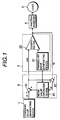
- FIG.1 is a block diagram showing the construction of an embodiment in accordance with the present invention.
- FIG.2 is a chart explaining a cause producing a problem to be solved by the present invention.
- FIG.3 is a chart explaining an operation of the present invention.
- FIG.4 is a chart explaining an operation when the present invention is applied to a discrete time system.
- FIG.5 is charts showing examples of simulation results where an induction motor is driven by pulse width modulation of the prior art and the pulse width modulation according to the present invention.
- an embodiment of the present invention will be described in detail below, referring to an inverter control system of FIG.1.
- a command value generating unit 1 an output voltage command value v r for an inverter 4 is generated.
- a pulse compensation unit 6 a signal V ref is output based on the output v r of the command value generating unit 1.
- a pulse width modulation pulse generating unit 2 receives the output signal V ref of the pulse compensation unit 6, and generates a pulse width modulation pulse v p corresponding to the signal V ref .
- the inverter control system is connected to an inverter 4 which outputs alternating current from direct current by driving switching elements composing the inverter based on the pulse width modulation signal of v p , and a load 5 such as a motor is connected in the alternating current output side of the inverter system.
- the output signal v p of the pulse width modulation pulse generating unit 2 is fed back to the unit 6.
- the unit 2 is a well-known pulse width modulation pulse generating unit which generates a pulse width modulation pulse v p by comparing a carrier signal of continuous triangular-wave having a constant period output from a triangular-wave generating unit with the signal V ref using a comparater 22.
- the present invention is characterized by the pulse compensation unit 6 which is composed of a subtracter 63 for calculating a difference of the signal V ref input to the pulse width modulation pulse generating unit and an output v p of pulse width modulation pulse, an average value calculating unit for calculating an average value v e of the output of the subtracter 63 every one-half period of a triangular wave output from the triangular-wave generating unit, and an adder 62 for adding the output v e of the average value calculating unit to the command value v r to output the signal V ref .
- the pulse compensation unit 6 which is composed of a subtracter 63 for calculating a difference of the signal V ref input to the pulse width modulation pulse generating unit and an output v p of pulse width modulation pulse, an average value calculating unit for calculating an average value v e of the output of the subtracter 63 every one-half period of a triangular wave output from the triangular-wave generating unit, and an adder 62 for adding
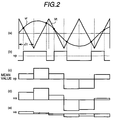
- FIG.2 An inverter command value v r and a triangular wave v t are shown in FIG.2 (a), an output v p of the pulse width modulation pulse generating unit is shown in (b), an average value (time product) of v p over a one-half period of the triangular wave is shown in (c), an average value (time product) of the command vale v r over a one-half period of the triangular wave is shown in (d), and a difference v e between the average value of V r and the average value of V p is shown in (e).
- the pulse compensation unit 6 is introduced.
- a difference between a voltage v p and a command value is calculated, and a time average v e of the difference over a one-half period ⁇ t of the triangular wave is calculated by the average value calculating unit 61, and the result is added to a command value v r .
- numeral 62 is an adder
- 63 a subtractor
- a command value in the next pulse calculation period following to a pulse calculation period where a difference v e is generated is set to v r +v e .
- a pulse reflected v e is generated in the output v p of the pulse calculation unit 2. Therefore, the difference v e in the voltage is certainly output in the next calculation period following to the calculation period where the difference v e is generated.
- shortage in compensation is reflected on the further next pulse. Therefore, even in such a case, v e can be properly compensated.
- the average voltage of command vales and the average value of output pulses agrees and the difference between them becomes zero when they are counted over several number of pulse calculation periods. That is, it is possible to eliminate the component of lower order harmonics and the component of fractional harmonics which have a long period and cause a low frequency pulsating current.
- the pulse width modulation pulse may be calculated by multiplying a gain to the average value v e of the difference between the command value and the pulse width modulation pulse, and adding the calculated result to the command value, if necessary.
- the command signal is a periodic function such as a sinusoidal wave function or a triangular wave function
- an average voltage of the command values may be easily calculated by preparing a function integrating the command signal in advance and by obtaining an average voltage of the command value using the integrated function.
- the triangular wave is a hypothetical wave and a command value is sampled at a timing ⁇ t corresponding to a one-half period of the triangular wave (hollow circles in the figure indicate sampling points).
- a pulse width modulation pulse v p is calculated based on the magnitude of the sampled value.
- the difference v e can be calculated and the pulse can be compensated as the same as in the continuous time system. Thereby, occurrence of the lower order harmonics and the fractional order harmonics can be prevented.
- pulsation in the discrete time system is larger than pulsation in the continuous time system. Therefore, the effect of the present invention appears more clearly in the discrete time system.
- FIG.5 shows simulation results where an electric power converter having an induction motor as the load is driven by an asynchronous pulse width modulation. inverter controlled by the prior art and by the pulse width modulation control according to the present invention.
- a case where the ratio n of the carrier frequency to the frequency of the command is 7.8 smaller than 10.
- FIG.5 (a) shows a case without the pulse compensation. Because there exists a difference between the average value of the command value over the pulse calculation period, pulsation of low frequency (fractional order harmonics) occurs.
- FIG.5 (b) shows the effect of the present invention.
- the pulse compensation has been performed suing the average value of voltage difference as the same as for the continuous time system.
- most method employ a construction where time of changing pulse from ON to OFF or from OFF to ON based on v r is calculated and then the state of pulse is changed based on the time.
- the same effect as in the case of performing pulse compensation using the average value of the voltage difference can be also obtained by determining pulse generating time by adding time which is determined by converting v e to pulse changing time to pulse changing time which is determined from only v r , and then by generating pulse width modulation pulse using the pulse generating time.
- an asynchronous pulse width modulation control system which can prevent generation of lower order harmonics and fractional order harmonics even at a low carrier frequency.
- a switching frequency of an electric power converter can be lowered. Therefore, the efficiency of the electric power converter cane improved and at the same time the system can be made small in size and light in weight.
Abstract
In pulse width modulation control for an electric power converter, occurrence of lower order harmonics, in order to suppress fractional order harmonics and direct current component even in a condition where a carrier frequency is several times as small as a frequency of a command value, pulse width modulation pulses for driving semiconductor elements composing an electric converter are calculated by comparing a command signal from a command value generating means with a carrier signal of a continuous triangular-wave having a constant period, which comprises a means for separately calculating a command value of the command signal from the command value generating means and a time product of the pulse width modulation pulses and calculating a difference value between the both time products, the pulse width modulation pulse being calculated by the difference value to the command signal from the command value generating means.
Description
- The present invention relates to a system for performing pulse width modulation control to an electric power converter such as a traction inverter, a supply converter and the like, and more particularly to a pulse width modulation control system for an electric converter capable of operating an inverter without generating low frequency pulsation in voltage and current when a ratio of switching frequency to inverter operating frequency is low.
- As pulse width modulation control methods having been used, there is a sub harmonic method in which pulse width modulation pulses for driving an inverter are generated by comparing a carrier signal of continuous triangular-wave with a constant frequency with an inverter output command value. Further, the pulse width modulation method can be roughly classified into an asynchronous pulse width control method and a synchronous pulse width modulation method which will be described below.
- In the asynchronous pulse width modulation control, when a frequency of the triangular-wave carrier (herein after referred to as "carrier frequency") is high enough compared to a frequency of the command value, the carrier frequency is fixed to a constant value and only the frequency of the command value is varied. For example, such asynchronous pulse width modulation control is disclosed in US Patent 5,467,262.
- In the synchronous pulse width modulation control, when a carrier frequency comparably near a frequency of the command value, the carrier frequency is always set to an integer times of the command value. In that time, the carrier frequency and a ratio of the carrier frequency to the frequency of the command value are varied according to the frequency of the command value.
- In a case of the asynchronous pulse width modulation control, it is required that the carrier frequency is sufficiently higher then the frequency of the command value, and the ratio of the carrier frequency to the frequency of the command value is generally required to be larger than around fifteen. When the ratio is smaller than this value, low order harmonics are increased and fractional order harmonics are generated. Therefore, current ripple becomes large, and consequently large capacity switching elements are required. In addition to this, when a motor is driven, there occurs pulsation in the torque.
- Although such problems can be solved by setting the carrier frequency to a sufficiently high value, there occurs another problem that the switching loss increases and accordingly the efficiency of the inverter is decreased. Further, for a large capacity inverter, there is a limitation in available switching elements, and therefore the carrier frequency cannot physically be set to a high value.
- On the other hand, in a case of the synchronous pulse width modulation control, even when the carrier frequency is low, harmonics can be suppressed to a certain degree and occurrence of the fractional order harmonics can be prevented. However, the carrier frequency and number of pulses are required to be switched depending on the frequency of a command value (determined by a ratio of the carrier frequency to the frequency of the command value), there arises a problem in that the control becomes complex and pulsation accompanied by switching of number of pulses (switching shock) occurs.
- In addition to this, when the synchronous pulse width modulation control is employed for an electric vehicle or an elevator, the passengers feel uncomfortable about sound due to magnetic noise.
- An object of the present invention is to provide an asynchronous pulse width modulation control system which can prevent increase of lower order harmonics and occurrence of fractional order harmonics even when the ratio of the switching frequency to the operating frequency of an inverter is small.
- The present invention is characterized by a pulse width modulation control system in which pulse width modulation pulses for driving semiconductor elements composing an electric converter are calculated by comparing a command signal from a command value generating means with a carrier signal of a continuous triangular-wave having a constant period, which comprises a means for separately calculating a command value of the command signal from the command value generating means and a time product of the pulse width modulation pulses and calculating a difference value between the both time products, the pulse width modulation pulse being calculated by the difference value to the command signal from the command value generating means.
- According to the present invention, since the sum of output pulse widths agrees with the sum of the command value by adding the difference between the time product of the command value and the time product of the pulse width modulation pulse to the command value, occurrence of unbalance between widths of positive pulse and negative pulse can be prevented and generation of lower order harmonics and fractional harmonics can be prevented.
- FIG.1 is a block diagram showing the construction of an embodiment in accordance with the present invention.
- FIG.2 is a chart explaining a cause producing a problem to be solved by the present invention.
- FIG.3 is a chart explaining an operation of the present invention.
- FIG.4 is a chart explaining an operation when the present invention is applied to a discrete time system.
- FIG.5 is charts showing examples of simulation results where an induction motor is driven by pulse width modulation of the prior art and the pulse width modulation according to the present invention.
- An embodiment of the present invention will be described in detail below, referring to an inverter control system of FIG.1. In a command value generating unit 1, an output voltage command value vr for an inverter 4 is generated. In a
pulse compensation unit 6, a signal Vref is output based on the output vr of the command value generating unit 1. A pulse width modulationpulse generating unit 2 receives the output signal Vref of thepulse compensation unit 6, and generates a pulse width modulation pulse vp corresponding to the signal Vref. Further, the inverter control system is connected to an inverter 4 which outputs alternating current from direct current by driving switching elements composing the inverter based on the pulse width modulation signal of vp, and aload 5 such as a motor is connected in the alternating current output side of the inverter system. - The output signal vp of the pulse width modulation
pulse generating unit 2 is fed back to theunit 6. Theunit 2 is a well-known pulse width modulation pulse generating unit which generates a pulse width modulation pulse vp by comparing a carrier signal of continuous triangular-wave having a constant period output from a triangular-wave generating unit with the signal Vref using acomparater 22. - The present invention is characterized by the
pulse compensation unit 6 which is composed of asubtracter 63 for calculating a difference of the signal Vref input to the pulse width modulation pulse generating unit and an output vp of pulse width modulation pulse, an average value calculating unit for calculating an average value ve of the output of thesubtracter 63 every one-half period of a triangular wave output from the triangular-wave generating unit, and anadder 62 for adding the output ve of the average value calculating unit to the command value vr to output the signal Vref. - Operation of the pulse compensation method according to the present invention will be described below, referring to FIG.2 and FIG.3. In order to make it easy to understand, description will be made by employing the conventional triangular-wave comparing method as an example. An inverter command value vr and a triangular wave vt are shown in FIG.2 (a), an output vp of the pulse width modulation pulse generating unit is shown in (b), an average value (time product) of vp over a one-half period of the triangular wave is shown in (c), an average value (time product) of the command vale vr over a one-half period of the triangular wave is shown in (d), and a difference ve between the average value of Vr and the average value of Vp is shown in (e). The character Δt is a one-half period of the triangular wave, and

- Description will be made below on the principle of generating lower order harmonics and fractional order harmonics in the asynchronous pulse width modulation and on the pulse compensation method for suppressing the lower order harmonics and the fractional order harmonics, referring to FIG.2.
- If an average value va of a modulated wave in Δt is accurately reflected on an output pulse vp of the pulse width modulation, lower order harmonics and fractional order harmonics cannot be generated. However, as shown in FIG.2 the average value of the modulated wave and the voltage vp reflected on the pulse width modulation pulse do not always agree. As a result, a difference ve between the average value of the modulated wave and the voltage reflected on the pulse width modulation pulse is generated, which causes lower order harmonics and fractional order harmonics and low frequency pulsation current flows.
- In the present invention, in order to suppress occurrence of the lower order harmonics and the fractional order harmonics, the
pulse compensation unit 6 is introduced. In thepulse comensation unit 6, a difference between a voltage vp and a command value is calculated, and a time average ve of the difference over a one-half period Δt of the triangular wave is calculated by the averagevalue calculating unit 61, and the result is added to a command value vr. - Here,
numeral 62 is an adder, 63 a subtractor. - Therefore, as shown in FIG.3, a command value in the next pulse calculation period following to a pulse calculation period where a difference ve is generated is set to vr+ve. As the result, a pulse reflected ve is generated in the output vp of the
pulse calculation unit 2. Therefore, the difference ve in the voltage is certainly output in the next calculation period following to the calculation period where the difference ve is generated. In a case where a pulse to be generated cannot be obtained because the pulse to be generated based on vr+ve is larger than the maximum generable pulse or smaller than the minimum generable pulse, shortage in compensation is reflected on the further next pulse. Therefore, even in such a case, ve can be properly compensated. - As described above, by repeating of calculating an average value of difference between a command value and an output pulse and adding the average value of difference to a command value vr in the next pulse calculation period, the average voltage of command vales and the average value of output pulses agrees and the difference between them becomes zero when they are counted over several number of pulse calculation periods. That is, it is possible to eliminate the component of lower order harmonics and the component of fractional harmonics which have a long period and cause a low frequency pulsating current.
- Thereby, occurrence of low frequency pulsation can be suppressed. Further, the pulse width modulation pulse may be calculated by multiplying a gain to the average value ve of the difference between the command value and the pulse width modulation pulse, and adding the calculated result to the command value, if necessary. Furthermore, when the command signal is a periodic function such as a sinusoidal wave function or a triangular wave function, an average voltage of the command values may be easily calculated by preparing a function integrating the command signal in advance and by obtaining an average voltage of the command value using the integrated function.
- Description will be made below on operation of a system in which the embodiment of FIG.1 is operated using a discrete time system such as software or a digital circuit. The signals and the marks of FIG.4 corresponding to those of FIG.2 are indicated by the same reference characters. In a case of a discrete time system, it is impossible to continuously monitor the command vale, and when a pulse width modulation pulse vp is calculated with software, the pulse width modulation pulse is not calculated by directly comparing the command vale and the triangular wave as shown in FIG.2. Although both of the command value vr and the triangular wave are drawn together in FIG.4, the triangular wave is a hypothetical wave and a command value is sampled at a timing Δt corresponding to a one-half period of the triangular wave (hollow circles in the figure indicate sampling points). A pulse width modulation pulse vp is calculated based on the magnitude of the sampled value.
- In this method, when number of samplings becomes small compared to the frequency of the command value (when the frequency of the command value becomes large),the difference ve between the command value vr and the average value of vp becomes larger comparing to the case of continuous time system. Therefore, in the discrete time system, larger lower order harmonics and larger fractional order harmonics are produced and pulsation in current also becomes larger. When the command value vr is a periodical function such as a sinusoidal wave function, the average value of the command value vr can be easily and accurately obtained by preparing an integrated function of the command value in advance as described above even in the discrete time system. By subtracting an average of vp from an average of a command value vr, the difference ve can be calculated and the pulse can be compensated as the same as in the continuous time system. Thereby, occurrence of the lower order harmonics and the fractional order harmonics can be prevented. As described above, pulsation in the discrete time system is larger than pulsation in the continuous time system. Therefore, the effect of the present invention appears more clearly in the discrete time system.
- FIG.5 shows simulation results where an electric power converter having an induction motor as the load is driven by an asynchronous pulse width modulation. inverter controlled by the prior art and by the pulse width modulation control according to the present invention. In order to clearly show the effect of the present invention against the prior art, a case where the ratio n of the carrier frequency to the frequency of the command is 7.8 smaller than 10. FIG.5 (a) shows a case without the pulse compensation. Because there exists a difference between the average value of the command value over the pulse calculation period, pulsation of low frequency (fractional order harmonics) occurs. On the other hand, in a case of according to the present invention, there is no low frequency pulsation in current as shown in FIG.5 (b), which shows the effect of the present invention.
- For a discrete time system, the pulse compensation has been performed suing the average value of voltage difference as the same as for the continuous time system. In a case of the discrete system, particularly in a case of generating pulse width modulation pulses using software, most method employ a construction where time of changing pulse from ON to OFF or from OFF to ON based on vr is calculated and then the state of pulse is changed based on the time. In this case, the same effect as in the case of performing pulse compensation using the average value of the voltage difference can be also obtained by determining pulse generating time by adding time which is determined by converting ve to pulse changing time to pulse changing time which is determined from only vr, and then by generating pulse width modulation pulse using the pulse generating time.
- Although the above embodiments have been described by taking an inverter as an example, it is needless to say that the present invention can be applied to a converter which converts alternating current to direct current.
- According to the present invention, it is possible to provide an asynchronous pulse width modulation control system which can prevent generation of lower order harmonics and fractional order harmonics even at a low carrier frequency.
- Further, by employing the present invention, a switching frequency of an electric power converter can be lowered. Therefore, the efficiency of the electric power converter cane improved and at the same time the system can be made small in size and light in weight.
Claims (6)
- A pulse width modulation control system for a electric power converter in which pulse width modulation pulses for driving semiconductor elements composing an electric converter are calculated by comparing a command signal from a command value generating means with a carrier signal of a continuous triangular-wave having a constant period, which comprises:means for separately calculating a command value of said command signal from said command value generating means and a time product of said pulse width modulation pulses and calculating a difference value between the both time products, said pulse width modulation pulse being calculated by said difference value to said command signal from said command value generating means.
- A pulse width modulation control system for a electric power converter in which pulse width modulation pulses for driving semiconductor elements composing an electric converter are calculated by capturing a command signal from a command value generating means every predetermined time period and calculating a pulse (pulse width modulation pulse) having a width corresponding to a magnitude of said command signal, which comprises:means for separately calculating a command value of said command signal from said command value generating means and a time product of said pulse width modulation pulses and calculating a difference value between the both time products, said pulse width modulation pulse being calculated by said difference value to said command signal from said command value generating means.
- A pulse width modulation control system according to claim 1, wherein said pulse width modulation pulse is calculated by setting a calculation period for calculating said pulse width modulation pulse to a one-half period of said triangular-wave carrier signal, calculating a difference between an average value of said command values and an average value of said pulse width modulation pulses for every said calculation period, and adding said difference to said command value for the next pulse calculation period.
- A pulse width modulation control system according to claim 2, wherein said pulse width modulation pulse is calculated by calculating a difference between an average value of said command values and an average value of said pulse width modulation pulses every said calculation period for calculating said pulse width modulation pulse, and adding said difference to said command value for the next pulse calculation period.
- A pulse width modulation control system according to any one of claim 3 and claim 4, wherein when said command value is a periodic function, an average value of said command values is calculated using a function obtained in advance by integrating said periodic function.
- A pulse width modulation control system according to any one of claim 1 to claim 5, wherein said pulse width modulation pulse is calculated by multiplying a gain to the difference between said average value of the command values and said average value of the pulse width modulation pulses, and adding the calculated result to said command value.
Applications Claiming Priority (2)
| Application Number | Priority Date | Filing Date | Title |
|---|---|---|---|
| JP04446096A JP3233005B2 (en) | 1996-03-01 | 1996-03-01 | PWM controller |
| JP44460/96 | 1996-03-01 |
Publications (2)
| Publication Number | Publication Date |
|---|---|
| EP0793335A2 true EP0793335A2 (en) | 1997-09-03 |
| EP0793335A3 EP0793335A3 (en) | 1998-12-16 |
Family
ID=12692113
Family Applications (1)
| Application Number | Title | Priority Date | Filing Date |
|---|---|---|---|
| EP97102696A Withdrawn EP0793335A3 (en) | 1996-03-01 | 1997-02-19 | Pulse width moldulation control system for electric power converter |
Country Status (9)
| Country | Link |
|---|---|
| US (1) | US5781423A (en) |
| EP (1) | EP0793335A3 (en) |
| JP (1) | JP3233005B2 (en) |
| KR (1) | KR970068111A (en) |
| CN (1) | CN1057879C (en) |
| AU (1) | AU689737B2 (en) |
| BR (1) | BR9701135B1 (en) |
| IN (1) | IN192459B (en) |
| ZA (1) | ZA971125B (en) |
Cited By (1)
| Publication number | Priority date | Publication date | Assignee | Title |
|---|---|---|---|---|
| CN108681327A (en) * | 2018-04-24 | 2018-10-19 | 电子科技大学 | Quadrotor flight control method based on fractional order saturation function switching law |
Families Citing this family (13)
| Publication number | Priority date | Publication date | Assignee | Title |
|---|---|---|---|---|
| US5903449A (en) * | 1998-06-09 | 1999-05-11 | General Electric Company | Bi-directional power control system for voltage converter |
| JP4655400B2 (en) * | 2000-05-30 | 2011-03-23 | アイシン精機株式会社 | Motor rotation pulse generation circuit for DC motor |
| US6940926B1 (en) * | 2001-03-05 | 2005-09-06 | Skyworks Solutions, Inc. | Digital phase/frequency detector |
| TWI312223B (en) * | 2003-11-14 | 2009-07-11 | Beyond Innovation Tech Co Ltd | A pulse width modulation control circuit and the loading system of its application |
| JP4085976B2 (en) * | 2003-12-25 | 2008-05-14 | 日産自動車株式会社 | Inverter control device and control method |
| JP4742230B2 (en) * | 2004-12-07 | 2011-08-10 | 富士電機株式会社 | PWM pulse generation method |
| DE112006003912B4 (en) | 2006-06-16 | 2014-05-22 | Mitsubishi Electric Corp. | Control device for energy converters |
| US7782005B2 (en) * | 2006-11-07 | 2010-08-24 | Nissan Motor Co., Ltd. | Power converter control |
| KR101300380B1 (en) * | 2012-03-02 | 2013-08-29 | 엘에스산전 주식회사 | Method for stabilizing inverter output current |
| JP6581373B2 (en) * | 2015-03-24 | 2019-09-25 | 株式会社日立産機システム | Motor control device |
| JP6414513B2 (en) * | 2015-06-05 | 2018-10-31 | アイシン・エィ・ダブリュ株式会社 | Rotating electrical machine control device |
| CN114992768B (en) * | 2022-05-20 | 2023-08-04 | 宁波奥克斯电气股份有限公司 | PWM modulation method and device, air conditioner and readable storage medium |
| JP2023177398A (en) * | 2022-06-02 | 2023-12-14 | 三菱電機株式会社 | Controller for ac rotary electric machine |
Citations (1)
| Publication number | Priority date | Publication date | Assignee | Title |
|---|---|---|---|---|
| US5467262A (en) * | 1992-06-04 | 1995-11-14 | Hitachi, Ltd. | Electric power converting apparatus |
Family Cites Families (10)
| Publication number | Priority date | Publication date | Assignee | Title |
|---|---|---|---|---|
| US515386A (en) * | 1894-02-27 | Jonas weiststrom | ||
| EP0105215B1 (en) * | 1982-09-07 | 1987-03-04 | Hitachi, Ltd. | Control apparatus for ac motors |
| JPH0667205B2 (en) * | 1983-02-04 | 1994-08-24 | 株式会社日立製作所 | PWM pulse generator |
| EP0243840B1 (en) * | 1986-04-22 | 1992-12-02 | Mitsubishi Denki Kabushiki Kaisha | Control circuit used for a power conversion apparatus |
| US4891744A (en) * | 1987-11-20 | 1990-01-02 | Mitsubishi Denki Kaubshiki Kaisha | Power converter control circuit |
| CA1313219C (en) * | 1988-10-07 | 1993-01-26 | Boon-Teck Ooi | Pulse width modulation high voltage direct current transmission system and converter |
| US5481451A (en) * | 1992-10-30 | 1996-01-02 | Arex Electronics Corporation | AC-to-AC power inverter apparatus functioning without smoothing capacitor, and control method thereof |
| US5377092A (en) * | 1992-11-16 | 1994-12-27 | International Power Machines | Method and apparatus for harmonic distortion correction |
| CA2114679C (en) * | 1993-02-04 | 1997-07-01 | Shigeru Tanaka | Power converter control system |
| US5657215A (en) * | 1995-08-29 | 1997-08-12 | Compaq Computer Corporation | Controlling switch-Mode power conversion |
-
1996
- 1996-03-01 JP JP04446096A patent/JP3233005B2/en not_active Expired - Fee Related
-
1997
- 1997-02-05 IN IN209CA1997 patent/IN192459B/en unknown
- 1997-02-07 US US08/797,621 patent/US5781423A/en not_active Expired - Lifetime
- 1997-02-11 ZA ZA9701125A patent/ZA971125B/en unknown
- 1997-02-14 AU AU12680/97A patent/AU689737B2/en not_active Ceased
- 1997-02-19 KR KR1019970004956A patent/KR970068111A/en not_active Application Discontinuation
- 1997-02-19 EP EP97102696A patent/EP0793335A3/en not_active Withdrawn
- 1997-02-28 BR BRPI9701135-5A patent/BR9701135B1/en not_active IP Right Cessation
- 1997-02-28 CN CN97103001A patent/CN1057879C/en not_active Expired - Fee Related
Patent Citations (1)
| Publication number | Priority date | Publication date | Assignee | Title |
|---|---|---|---|---|
| US5467262A (en) * | 1992-06-04 | 1995-11-14 | Hitachi, Ltd. | Electric power converting apparatus |
Non-Patent Citations (1)
| Title |
|---|
| GEZA JOOS ET AL: "A MODEL REFERENCE ADAPTIVE PWM TECHNIQUE" IEEE TRANSACTIONS ON POWER ELECTRONICS, vol. 5, no. 4, 1 October 1990, pages 485-494, XP000204296 * |
Cited By (2)
| Publication number | Priority date | Publication date | Assignee | Title |
|---|---|---|---|---|
| CN108681327A (en) * | 2018-04-24 | 2018-10-19 | 电子科技大学 | Quadrotor flight control method based on fractional order saturation function switching law |
| CN108681327B (en) * | 2018-04-24 | 2020-05-08 | 电子科技大学 | Four-rotor flight control method based on fractional order saturation function switching control law |
Also Published As
| Publication number | Publication date |
|---|---|
| BR9701135B1 (en) | 2009-01-13 |
| CN1162216A (en) | 1997-10-15 |
| IN192459B (en) | 2004-04-24 |
| US5781423A (en) | 1998-07-14 |
| ZA971125B (en) | 1997-08-25 |
| CN1057879C (en) | 2000-10-25 |
| EP0793335A3 (en) | 1998-12-16 |
| AU689737B2 (en) | 1998-04-02 |
| AU1268097A (en) | 1997-09-25 |
| BR9701135A (en) | 1998-12-15 |
| JPH09238472A (en) | 1997-09-09 |
| KR970068111A (en) | 1997-10-13 |
| JP3233005B2 (en) | 2001-11-26 |
Similar Documents
| Publication | Publication Date | Title |
|---|---|---|
| EP0793335A2 (en) | Pulse width moldulation control system for electric power converter | |
| AU598379B2 (en) | Inverter control apparatus | |
| EP0417805B1 (en) | Control method and device for AC motor | |
| US5686807A (en) | Torque control system for AC motor | |
| EP0658969A2 (en) | Electric power conversion equipment | |
| US4924168A (en) | Control apparatus for PWM-controlled, variable voltage/variable frequency inverters | |
| EP0808016A1 (en) | PWM inverter apparatus | |
| US4516038A (en) | Triangle wave generator | |
| US5959855A (en) | Voltage control with feedback utilizing analog and digital control signals | |
| JP2933846B2 (en) | PWM inverter with dead time correction function | |
| JP3265397B2 (en) | Power converter control method and power converter using the method | |
| JPS61262006A (en) | Controller of induction motor for vehicle | |
| EP0293844A2 (en) | A control apparatus for PWM-controlled, variable voltage/variable frequency inverters | |
| JP3116698B2 (en) | Inverter voltage detector | |
| JPH08172722A (en) | Overcurrent-takeout preventive apparatus | |
| JP2735238B2 (en) | Uninterruptible power supply control method | |
| JPH06178550A (en) | Current control device of vvvf inverter | |
| JP3188097B2 (en) | Inverter control device | |
| RU2214618C2 (en) | Control method using pulse-width modulation | |
| JP3252598B2 (en) | converter | |
| US20030086281A1 (en) | Converter circuit arrangement, as well as a method for matching a variable DC voltage | |
| RU2046528C1 (en) | Method for controlling follow-up pulsed converter | |
| JP2644255B2 (en) | Inverter control method | |
| JP2779743B2 (en) | Power conversion controller filter | |
| RU2039955C1 (en) | Method of measurement of electromagnetic moment of induction motor |
Legal Events
| Date | Code | Title | Description |
|---|---|---|---|
| PUAI | Public reference made under article 153(3) epc to a published international application that has entered the european phase |
Free format text: ORIGINAL CODE: 0009012 |
|
| AK | Designated contracting states |
Kind code of ref document: A2 Designated state(s): CH DE FR LI |
|
| PUAL | Search report despatched |
Free format text: ORIGINAL CODE: 0009013 |
|
| AK | Designated contracting states |
Kind code of ref document: A3 Designated state(s): CH DE FR LI |
|
| 17P | Request for examination filed |
Effective date: 19981221 |
|
| STAA | Information on the status of an ep patent application or granted ep patent |
Free format text: STATUS: THE APPLICATION IS DEEMED TO BE WITHDRAWN |
|
| 18D | Application deemed to be withdrawn |
Effective date: 20000901 |