EP0794560A2 - Production method for insulated semiconductor device - Google Patents
Production method for insulated semiconductor device Download PDFInfo
- Publication number
- EP0794560A2 EP0794560A2 EP97103714A EP97103714A EP0794560A2 EP 0794560 A2 EP0794560 A2 EP 0794560A2 EP 97103714 A EP97103714 A EP 97103714A EP 97103714 A EP97103714 A EP 97103714A EP 0794560 A2 EP0794560 A2 EP 0794560A2
- Authority
- EP
- European Patent Office
- Prior art keywords
- leads
- lead portions
- resin
- semiconductor device
- hoop frame
- Prior art date
- Legal status (The legal status is an assumption and is not a legal conclusion. Google has not performed a legal analysis and makes no representation as to the accuracy of the status listed.)
- Withdrawn
Links
Images


Classifications
-
- H—ELECTRICITY
- H01—ELECTRIC ELEMENTS
- H01L—SEMICONDUCTOR DEVICES NOT COVERED BY CLASS H10
- H01L21/00—Processes or apparatus adapted for the manufacture or treatment of semiconductor or solid state devices or of parts thereof
- H01L21/02—Manufacture or treatment of semiconductor devices or of parts thereof
- H01L21/04—Manufacture or treatment of semiconductor devices or of parts thereof the devices having at least one potential-jump barrier or surface barrier, e.g. PN junction, depletion layer or carrier concentration layer
- H01L21/50—Assembly of semiconductor devices using processes or apparatus not provided for in a single one of the subgroups H01L21/06 - H01L21/326, e.g. sealing of a cap to a base of a container
- H01L21/56—Encapsulations, e.g. encapsulation layers, coatings
- H01L21/565—Moulds
-
- H—ELECTRICITY
- H01—ELECTRIC ELEMENTS
- H01L—SEMICONDUCTOR DEVICES NOT COVERED BY CLASS H10
- H01L23/00—Details of semiconductor or other solid state devices
- H01L23/48—Arrangements for conducting electric current to or from the solid state body in operation, e.g. leads, terminal arrangements ; Selection of materials therefor
- H01L23/488—Arrangements for conducting electric current to or from the solid state body in operation, e.g. leads, terminal arrangements ; Selection of materials therefor consisting of soldered or bonded constructions
- H01L23/495—Lead-frames or other flat leads
- H01L23/49541—Geometry of the lead-frame
- H01L23/49562—Geometry of the lead-frame for devices being provided for in H01L29/00
-
- H—ELECTRICITY
- H01—ELECTRIC ELEMENTS
- H01L—SEMICONDUCTOR DEVICES NOT COVERED BY CLASS H10
- H01L24/00—Arrangements for connecting or disconnecting semiconductor or solid-state bodies; Methods or apparatus related thereto
- H01L24/93—Batch processes
- H01L24/95—Batch processes at chip-level, i.e. with connecting carried out on a plurality of singulated devices, i.e. on diced chips
- H01L24/97—Batch processes at chip-level, i.e. with connecting carried out on a plurality of singulated devices, i.e. on diced chips the devices being connected to a common substrate, e.g. interposer, said common substrate being separable into individual assemblies after connecting
-
- H—ELECTRICITY
- H01—ELECTRIC ELEMENTS
- H01L—SEMICONDUCTOR DEVICES NOT COVERED BY CLASS H10
- H01L2224/00—Indexing scheme for arrangements for connecting or disconnecting semiconductor or solid-state bodies and methods related thereto as covered by H01L24/00
- H01L2224/01—Means for bonding being attached to, or being formed on, the surface to be connected, e.g. chip-to-package, die-attach, "first-level" interconnects; Manufacturing methods related thereto
- H01L2224/42—Wire connectors; Manufacturing methods related thereto
- H01L2224/47—Structure, shape, material or disposition of the wire connectors after the connecting process
- H01L2224/48—Structure, shape, material or disposition of the wire connectors after the connecting process of an individual wire connector
- H01L2224/4805—Shape
- H01L2224/4809—Loop shape
- H01L2224/48091—Arched
-
- H—ELECTRICITY
- H01—ELECTRIC ELEMENTS
- H01L—SEMICONDUCTOR DEVICES NOT COVERED BY CLASS H10
- H01L2224/00—Indexing scheme for arrangements for connecting or disconnecting semiconductor or solid-state bodies and methods related thereto as covered by H01L24/00
- H01L2224/01—Means for bonding being attached to, or being formed on, the surface to be connected, e.g. chip-to-package, die-attach, "first-level" interconnects; Manufacturing methods related thereto
- H01L2224/42—Wire connectors; Manufacturing methods related thereto
- H01L2224/47—Structure, shape, material or disposition of the wire connectors after the connecting process
- H01L2224/48—Structure, shape, material or disposition of the wire connectors after the connecting process of an individual wire connector
- H01L2224/481—Disposition
- H01L2224/48151—Connecting between a semiconductor or solid-state body and an item not being a semiconductor or solid-state body, e.g. chip-to-substrate, chip-to-passive
- H01L2224/48221—Connecting between a semiconductor or solid-state body and an item not being a semiconductor or solid-state body, e.g. chip-to-substrate, chip-to-passive the body and the item being stacked
- H01L2224/48245—Connecting between a semiconductor or solid-state body and an item not being a semiconductor or solid-state body, e.g. chip-to-substrate, chip-to-passive the body and the item being stacked the item being metallic
- H01L2224/48247—Connecting between a semiconductor or solid-state body and an item not being a semiconductor or solid-state body, e.g. chip-to-substrate, chip-to-passive the body and the item being stacked the item being metallic connecting the wire to a bond pad of the item
-
- H—ELECTRICITY
- H01—ELECTRIC ELEMENTS
- H01L—SEMICONDUCTOR DEVICES NOT COVERED BY CLASS H10
- H01L2224/00—Indexing scheme for arrangements for connecting or disconnecting semiconductor or solid-state bodies and methods related thereto as covered by H01L24/00
- H01L2224/01—Means for bonding being attached to, or being formed on, the surface to be connected, e.g. chip-to-package, die-attach, "first-level" interconnects; Manufacturing methods related thereto
- H01L2224/42—Wire connectors; Manufacturing methods related thereto
- H01L2224/47—Structure, shape, material or disposition of the wire connectors after the connecting process
- H01L2224/48—Structure, shape, material or disposition of the wire connectors after the connecting process of an individual wire connector
- H01L2224/484—Connecting portions
- H01L2224/48463—Connecting portions the connecting portion on the bonding area of the semiconductor or solid-state body being a ball bond
- H01L2224/48465—Connecting portions the connecting portion on the bonding area of the semiconductor or solid-state body being a ball bond the other connecting portion not on the bonding area being a wedge bond, i.e. ball-to-wedge, regular stitch
-
- H—ELECTRICITY
- H01—ELECTRIC ELEMENTS
- H01L—SEMICONDUCTOR DEVICES NOT COVERED BY CLASS H10
- H01L2224/00—Indexing scheme for arrangements for connecting or disconnecting semiconductor or solid-state bodies and methods related thereto as covered by H01L24/00
- H01L2224/01—Means for bonding being attached to, or being formed on, the surface to be connected, e.g. chip-to-package, die-attach, "first-level" interconnects; Manufacturing methods related thereto
- H01L2224/42—Wire connectors; Manufacturing methods related thereto
- H01L2224/47—Structure, shape, material or disposition of the wire connectors after the connecting process
- H01L2224/49—Structure, shape, material or disposition of the wire connectors after the connecting process of a plurality of wire connectors
- H01L2224/491—Disposition
- H01L2224/4912—Layout
- H01L2224/49171—Fan-out arrangements
-
- H—ELECTRICITY
- H01—ELECTRIC ELEMENTS
- H01L—SEMICONDUCTOR DEVICES NOT COVERED BY CLASS H10
- H01L2224/00—Indexing scheme for arrangements for connecting or disconnecting semiconductor or solid-state bodies and methods related thereto as covered by H01L24/00
- H01L2224/01—Means for bonding being attached to, or being formed on, the surface to be connected, e.g. chip-to-package, die-attach, "first-level" interconnects; Manufacturing methods related thereto
- H01L2224/42—Wire connectors; Manufacturing methods related thereto
- H01L2224/47—Structure, shape, material or disposition of the wire connectors after the connecting process
- H01L2224/49—Structure, shape, material or disposition of the wire connectors after the connecting process of a plurality of wire connectors
- H01L2224/491—Disposition
- H01L2224/4912—Layout
- H01L2224/49175—Parallel arrangements
-
- H—ELECTRICITY
- H01—ELECTRIC ELEMENTS
- H01L—SEMICONDUCTOR DEVICES NOT COVERED BY CLASS H10
- H01L24/00—Arrangements for connecting or disconnecting semiconductor or solid-state bodies; Methods or apparatus related thereto
- H01L24/01—Means for bonding being attached to, or being formed on, the surface to be connected, e.g. chip-to-package, die-attach, "first-level" interconnects; Manufacturing methods related thereto
- H01L24/42—Wire connectors; Manufacturing methods related thereto
- H01L24/47—Structure, shape, material or disposition of the wire connectors after the connecting process
- H01L24/48—Structure, shape, material or disposition of the wire connectors after the connecting process of an individual wire connector
-
- H—ELECTRICITY
- H01—ELECTRIC ELEMENTS
- H01L—SEMICONDUCTOR DEVICES NOT COVERED BY CLASS H10
- H01L24/00—Arrangements for connecting or disconnecting semiconductor or solid-state bodies; Methods or apparatus related thereto
- H01L24/01—Means for bonding being attached to, or being formed on, the surface to be connected, e.g. chip-to-package, die-attach, "first-level" interconnects; Manufacturing methods related thereto
- H01L24/42—Wire connectors; Manufacturing methods related thereto
- H01L24/47—Structure, shape, material or disposition of the wire connectors after the connecting process
- H01L24/49—Structure, shape, material or disposition of the wire connectors after the connecting process of a plurality of wire connectors
-
- H—ELECTRICITY
- H01—ELECTRIC ELEMENTS
- H01L—SEMICONDUCTOR DEVICES NOT COVERED BY CLASS H10
- H01L2924/00—Indexing scheme for arrangements or methods for connecting or disconnecting semiconductor or solid-state bodies as covered by H01L24/00
- H01L2924/0001—Technical content checked by a classifier
- H01L2924/00014—Technical content checked by a classifier the subject-matter covered by the group, the symbol of which is combined with the symbol of this group, being disclosed without further technical details
-
- H—ELECTRICITY
- H01—ELECTRIC ELEMENTS
- H01L—SEMICONDUCTOR DEVICES NOT COVERED BY CLASS H10
- H01L2924/00—Indexing scheme for arrangements or methods for connecting or disconnecting semiconductor or solid-state bodies as covered by H01L24/00
- H01L2924/01—Chemical elements
- H01L2924/01078—Platinum [Pt]
-
- H—ELECTRICITY
- H01—ELECTRIC ELEMENTS
- H01L—SEMICONDUCTOR DEVICES NOT COVERED BY CLASS H10
- H01L2924/00—Indexing scheme for arrangements or methods for connecting or disconnecting semiconductor or solid-state bodies as covered by H01L24/00
- H01L2924/15—Details of package parts other than the semiconductor or other solid state devices to be connected
- H01L2924/181—Encapsulation
Definitions
- This invention relates to a production method for an insulated semiconductor device.
- FIG. 12 illustrates a manner in which it is produced in six different steps A to F.
- a flat hoop frame having sets of lead portions having inner lead portions 3 is successively supplied from a frame supply apparatus to a die bonding apparatus (step A), and die bonding of a semiconductor pellet 11 on an island 10 of one of the inner lead portions 3 of each set of lead portions is performed (step B). Then, the flat hoop frame is supplied to a wire bonding apparatus via a buffer.
- the wire bonding apparatus performs wire bonding for a pad (not shown) of the semiconductor pellet 11 and the other inner lead portion 3 of the set of lead portions using wires 18 (step C). Then, the flat hoop frame is supplied to a resin filling apparatus via another buffer.
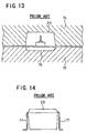
- the resin filling apparatus holds and pressurises the flat hoop frame between an upper metallic mold 14 and a lower metallic mold 15 as seen in FIG. 13, fills a resin into an upper metallic mold cavity 24 and a lower metallic mold cavity 16 above and below the flat hoop frame to embed the inner lead portions 3 of each set of lead portions in the resin (step D of FIG. 12), and then accommodates the flat hoop frame with the inner lead portions 3 embedded in the resin into a frame take-up apparatus.
- the flat hoop frame taken up by the frame take-up apparatus is then solder plated by a solder plating machine, whereafter it is supplied to and worked by, in the following steps E and F illustrated in FIG. 12, a composite apparatus (including a lead cutting apparatus, a lead shaping apparatus, a selection apparatus, a printing apparatus and a taping apparatus), by which it is taken up by a predetermined amount onto a shipment reel.
- such a semiconductor device 20 as shown in FIG. 14 is produced by the steps that, for a flat hoop frame supplied from a frame supply apparatus, a semiconductor pellet is die bonded to an island of a flat inner lead portion by a die bonding apparatus and then a pad of the semiconductor pellet and the other inner lead portions are wire bonded by a wire bonding apparatus, whereafter a resin is filled into upper and lower metallic mold cavities (24 and 16 in FIG. 13) by a resin filling apparatus and then solder plating is performed by a solder plating apparatus, and then the flat hoop frame is supplied to a composite apparatus.
- outer leads 17 are cut such that they have different lengths on the left side and the right side of the semiconductor device. Consequently, upon shaping of the outer leads 17 (refer to FIG. 14), they are not shaped in specified dimensions in terms of the vertical or height position, the lead width and the length of a flat face.
- the conventional method is disadvantageous also in that waste solder produced upon soldering sticks to and disturbs accurate positioning by a positioning stage or a positioning clamper.
- the conventional method is further disadvantageous in that, in the selection step, accurate measurement is disturbed by a dispersion in length of a flat face or inaccurate positioning.
- the conventional method is disadvantageous also in that, when the winding diameter on a reel increases, the operability is deteriorated, and the operation cannot be performed.
- leads of a flat hoop frame are shaped so that outer lead portions may be positioned at predetermined positions with respect to an outer profile of a semiconductor device after a resin is filled.
- a production method for an insulated semiconductor device comprising the steps of forming a flat hoop frame having a plurality of rows of sets of leads such that inner lead portions of the leads extend farther than corresponding resin filling centers so that outer lead portions of the leads may be positioned at predetermined positions with respect to outer profiles of semiconductor devices after resin is filled and supplying the flat hoop frame from a frame supply apparatus, shaping the inner lead portions of the leads of the flat hoop frame simultaneously for the plurality of rows and for a plurality of pitches by a lead shaping apparatus, performing die bonding of semiconductor pellets and wire bonding for the flat hoop frame, and filling, for each set of leads, resin into one of two cavities by a resin filling apparatus so that the outer lead portions of the leads of the flat hoop frame may be positioned at the predetermined positions with respect to the outer profiles of the semiconductor devices after the resin is filled.
- the production method for an insulated semiconductor device eliminates lead shaping processing by a composite apparatus. Consequently, various problems which otherwise originate from lead shaping by a composite apparatus including failure in shaping of outer lead portions with accurate dimensions, production of a gap between an outer lead portion and a portion of a resin block at which the outer lead portion is attached upon lead shaping, production of waster solder, inaccurate measurement of an outer lead foot portion by elongation upon selection and so forth are eliminated, and augmentation in quality, productivity and maintenance feasibility can be achieved.
- the inner lead portions of the leads of the flat hoop frame extend by a predetermined additional length farther than the positions of the individual resin filling centers.
- FIG. 2 illustrates different steps of a production process for an insulated semiconductor device to which the present invention is applied
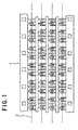
- FIG. 1 shows a flat hoop frame used for the production method illustrated in FIG. 2.
- the flat hoop frame is generally denoted at 1 and includes a large number of sets of leads having inner and outer lead portions arranged in a plurality of (four in FIG. 1) rows.
- the flat hoop frame 1 is formed such that, in each set of leads, inner lead portions extend farther than the position of a corresponding one of resin filling centers 2 for the individual rows with a lead shaping amount determined taking a semiconductor pellet thickness and a bonding wire height into consideration so that the outer lead portions may be positioned at predetermined positions with respect to the semiconductor device of the set.
- the flat hoop frame 1 supplied from a frame supply apparatus (refer to step A of FIG. 2) is successively subject, prior to the step of die bonding a semiconductor pellet to it, to simultaneous shaping of the inner lead portions 3 thereof for the plurality of rows (in the lateral direction) at a plurality of pitches (in the longitudinal direction) by a lead shaping apparatus mounted on the frame supply apparatus or on a die bonding apparatus (refer to step B of FIG. 2).
- the lead shaping apparatus may naturally be provided as a single machine.
- step C of FIG. 2 die bonding of a semiconductor pellet to each island 10
- wire bonding wire bonding
- step D of FIG. 2 resin is filled into only one of upper and lower metallic mold cavities by a resin filling apparatus so that the outer lead portions of the flat hoop frame may be positioned at predetermined positions with respect to the outer profiles of the semiconductor devices after the resin is filled (refer to step E of FIG. 2).
- the outer leads 17 are cut by a lead cutting apparatus (refer to step F of FIG. 2).
- the flat hoop frame 1 is formed such that the inner lead portions 3 in each set of leads extend farther than the position of the corresponding resin filling center 2 taking a lead shaping amount into consideration.
- the inner lead portions 3 in each set of leads and the island 10 extend farther than the resin filling center 2 by an amount corresponding to the lead shaping amount which is determined taking a semiconductor pellet thickness and a bonding wire height upon lead formation into consideration.
- FIG. 6 illustrates details of the steps performed by the frame supply apparatus, lead shaping apparatus and die bonding apparatus.
- the flat hoop frame 1 is fed from the frame supply apparatus 4 to the lead shaping apparatus 6 mounted at a location of the die bonding apparatus 5.
- the inner lead portions 3 of the flat hoop frame 1 are shaped downwardly into an L-shape simultaneously for the plurality of rows and the plurality of pitches by lead shaping punches 7 and a die 8 as seen in FIGS. 7(A) and 7(B) which illustrate a manner of lead shaping.
- the flat hoop frame 1 is supplied via a buffer 9 to the die bonding apparatus 5.
- FIG. 4(B) illustrates a manner in which the inner lead portions 3 are shaped downwardly into an L-shape by the lead shaping apparatus 6.
- step C of FIG. 2 die bonding of semiconductor pellets 11 on the islands 10 of the inner lead portions 3 of the flat hoop frame 1 supplied thereto is performed (refer to step C of FIG. 2).
- the flat hoop frame 1 is supplied to a wire bonding apparatus via another buffer.
- the flat hoop frame 1 supplied to the wire bonding apparatus pads of the semiconductor pellets 11 and the inner lead portions 3 are bonded using wires 18 by the wire bonding apparatus (refer to step E of FIG. 2 and also to FIG. 8(A)). After completion of the wire bonding, the flat hoop frame 1 is supplied to a resin filling apparatus via a further buffer.
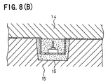
- the flat hoop frame 1 supplied to the resin filling apparatus is held between and pressurized by an upper metallic mold 14 and a lower metallic mold 15 as seen in FIG. 8(B), and then resin is filled only into lower metallic mold cavities 16. Thereafter, the flat hoop frame 1 is accommodated into a frame take-up machine.
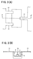
- a manner of a semiconductor device and outer leads of it after the resin is filled is shown in plan view in FIG. 3(A) and in sectional view taken along line A-A' of FIG. 3(A) in FIG. 3(B).
- the outer leads 17 of the semiconductor device filled with the resin are bent at an end face of the semiconductor device and then extend in the outward directions (leftward and rightward directions in FIGS. 3(A) and 3(B)) along the end face.
- the flat hoop frame 1 After taken up onto the frame take-up machine, the flat hoop frame 1 is solder plated by a solder plating apparatus. After the solder plating, the flat hoop frame 1 is supplied to and worked by a composite apparatus (refer to step F of FIG. 2) which includes a lead cutting apparatus, a selection apparatus, a printing apparatus and a taping apparatus, by which it is finally taken up by a predetermined amount onto a shipment reel. It is to be noted that the outer leads 17 are cut by the composite apparatus so that the outer leads 17 (foot portions) extends along the lower face of the semiconductor device 20 and project by a predetermined amount outwardly from the lower face as seen in FIG. 5.
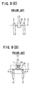
- FIG. 9(A) shows details of lead portions of a flat hoop frame which is employed for a production method for an insulated semiconductor device according to another embodiment of the present invention
- FIG. 9(B) shows details of the lead portions after inner lead shaping is performed using the production method for an insulated semiconductor device of the second embodiment
- FIG. 9(C) shows details of lead portions of a conventional flat hop frame
- FIG. 9(D) shows details of the lead portions of the flat hop frame of FIG. 9(C) after inner lead shaping is performed using a conventional method.
- FIGS. 10(A) and 10(B) show details of a resin filling metallic mold employed in the production method of the present embodiment.
- inner lead portions 3 are formed, taking a lead shaping amount into consideration, such that they are elongated farther than the position of a corresponding resin filling center 2.
- the inner lead portions 3 are shaped upwardly into an L-shape simultaneously for a plurality of rows and a plurality of pitches by a lead shaping apparatus (refer to FIG. 9(B)).
- the production method of the present embodiment is advantageous in that, by boding wires 18 obliquely in the wire bonding step, lead shaping (refer to FIG. 9(D) can be performed for the conventional flat hoop frame 1 (refer to FIG. 9(C)).
Abstract
Description
- This invention relates to a production method for an insulated semiconductor device.
- An exemplary one of conventional production methods for an insulated semiconductor device is first described with reference to FIG. 12 which illustrates a manner in which it is produced in six different steps A to F. A flat hoop frame having sets of lead portions having
inner lead portions 3 is successively supplied from a frame supply apparatus to a die bonding apparatus (step A), and die bonding of asemiconductor pellet 11 on anisland 10 of one of theinner lead portions 3 of each set of lead portions is performed (step B). Then, the flat hoop frame is supplied to a wire bonding apparatus via a buffer. - The wire bonding apparatus performs wire bonding for a pad (not shown) of the
semiconductor pellet 11 and the otherinner lead portion 3 of the set of lead portions using wires 18 (step C). Then, the flat hoop frame is supplied to a resin filling apparatus via another buffer. - The resin filling apparatus holds and pressurises the flat hoop frame between an upper
metallic mold 14 and a lowermetallic mold 15 as seen in FIG. 13, fills a resin into an uppermetallic mold cavity 24 and a lowermetallic mold cavity 16 above and below the flat hoop frame to embed theinner lead portions 3 of each set of lead portions in the resin (step D of FIG. 12), and then accommodates the flat hoop frame with theinner lead portions 3 embedded in the resin into a frame take-up apparatus. The flat hoop frame taken up by the frame take-up apparatus is then solder plated by a solder plating machine, whereafter it is supplied to and worked by, in the following steps E and F illustrated in FIG. 12, a composite apparatus (including a lead cutting apparatus, a lead shaping apparatus, a selection apparatus, a printing apparatus and a taping apparatus), by which it is taken up by a predetermined amount onto a shipment reel. - According to the conventional production method for a semiconductor device, such a
semiconductor device 20 as shown in FIG. 14 is produced by the steps that, for a flat hoop frame supplied from a frame supply apparatus, a semiconductor pellet is die bonded to an island of a flat inner lead portion by a die bonding apparatus and then a pad of the semiconductor pellet and the other inner lead portions are wire bonded by a wire bonding apparatus, whereafter a resin is filled into upper and lower metallic mold cavities (24 and 16 in FIG. 13) by a resin filling apparatus and then solder plating is performed by a solder plating apparatus, and then the flat hoop frame is supplied to a composite apparatus. Consequently, if the positions of the upper and lower metallic mold cavities (upper and lower caps) are displaced from each other when a resin is to be filled, then when the flat hoop frame is worked by the composite apparatus, since such working by the composite apparatus is performed with the flat hoop frame positioned with reference to the outer profile of the semiconductor device,outer leads 17 are cut such that they have different lengths on the left side and the right side of the semiconductor device. Consequently, upon shaping of the outer leads 17 (refer to FIG. 14), they are not shaped in specified dimensions in terms of the vertical or height position, the lead width and the length of a flat face. - The conventional method is disadvantageous also in that waste solder produced upon soldering sticks to and disturbs accurate positioning by a positioning stage or a positioning clamper.
- The conventional method is further disadvantageous in that, in the selection step, accurate measurement is disturbed by a dispersion in length of a flat face or inaccurate positioning.
- Further, while a flat hoop frame is produced by stamping, if inner lead portions are shaped upon the stamping, then when the flat hoop frame is taken up onto a supply reel, the leads are liable to be deformed.
- The conventional method is disadvantageous also in that, when the winding diameter on a reel increases, the operability is deteriorated, and the operation cannot be performed.
- It is an object of the present invention to provide a production method for an insulated semiconductor device which eliminates displacement between positions of upper and lower metallic mold cavities (between upper and lower caps) when a resin is filled to achieve improvement in quality and productivity.
- In order to attain the object described above, according to the present invention, before die bonding, leads of a flat hoop frame are shaped so that outer lead portions may be positioned at predetermined positions with respect to an outer profile of a semiconductor device after a resin is filled.
- More particularly, according to the present invention, there is provided a production method for an insulated semiconductor device, comprising the steps of forming a flat hoop frame having a plurality of rows of sets of leads such that inner lead portions of the leads extend farther than corresponding resin filling centers so that outer lead portions of the leads may be positioned at predetermined positions with respect to outer profiles of semiconductor devices after resin is filled and supplying the flat hoop frame from a frame supply apparatus, shaping the inner lead portions of the leads of the flat hoop frame simultaneously for the plurality of rows and for a plurality of pitches by a lead shaping apparatus, performing die bonding of semiconductor pellets and wire bonding for the flat hoop frame, and filling, for each set of leads, resin into one of two cavities by a resin filling apparatus so that the outer lead portions of the leads of the flat hoop frame may be positioned at the predetermined positions with respect to the outer profiles of the semiconductor devices after the resin is filled. Thus, since only one of upper and lower metallic mold cavities is required for resin filling, otherwise possible displacement between the positions of upper and lower metallic mold cavities (displacement between upper and lower caps) can be prevented.
- Further, the production method for an insulated semiconductor device eliminates lead shaping processing by a composite apparatus. Consequently, various problems which otherwise originate from lead shaping by a composite apparatus including failure in shaping of outer lead portions with accurate dimensions, production of a gap between an outer lead portion and a portion of a resin block at which the outer lead portion is attached upon lead shaping, production of waster solder, inaccurate measurement of an outer lead foot portion by elongation upon selection and so forth are eliminated, and augmentation in quality, productivity and maintenance feasibility can be achieved.
- Furthermore, since only one metallic mold cavity is required for the resin filling apparatus and a lead shaping apparatus of a composite apparatus is eliminated, reduction in cost for the metallic mold and the composite apparatus can be achieved.
- Preferably, the inner lead portions of the leads of the flat hoop frame extend by a predetermined additional length farther than the positions of the individual resin filling centers.
- The above and other objects, features and advantages of the present invention will become apparent from the following description and the appended claims, taken in conjunction with the accompanying drawings in which like parts or elements are denoted by like reference characters.
-
- FIG. 1 is a plan view of a flat hoop frame to which a production method for an insulated semiconductor device according to the present invention is applied;
- FIG. 2 is a schematic views illustrating different steps of a production method for an insulated semiconductor device according to a preferred embodiment of the present invention;
- FIG. 3(A) is a detailed plan view of a semiconductor device after a resin is filled in the production method illustrated in FIG. 2;
- FIG. 3(B) is a sectional view taken along line A-A' of FIG. 3(A);
- FIG. 4(A) is a detailed perspective view of frame lead portions of the flat hoop frame of FIG. 1 before they are shaped;
- FIG. 4(B) is a detailed perspective view of the frame lead portions of FIG. 4(A) after they are shaped in the production method illustrated in FIG. 2;
- FIG. 5 is a side elevational view of an insulated semiconductor device produced by the production method illustrated in FIG. 2;
- FIG. 6 is a schematic view illustrating detailed steps performed by a frame supply apparatus, a lead shaping apparatus and a die bonding apparatus in the production method illustrated in FIG. 2;
- FIG. 7(A) is a detailed plan view of an inner lead shaping section of the lead shaping apparatus shown in FIG. 6;
- FIG. 7(B) is a sectional view taken along line B-B' of FIG. 7(A);
- FIG. 8(A) is a detailed plan view of a portion of a resin filling metallic mold employed in the production method illustrated in FIG. 2;
- FIG. 8(B) is a sectional view taken along line B-B' of FIG. 8(A);
- FIG. 9(A) is a detailed perspective view of lead portions of a flat hoop frame employed for a production method for an insulated semiconductor device according to another embodiment of the present invention;
- FIG. 9(B) is a detailed perspective view of the lead portions after inner lead shaping is performed by the production method for an insulated semiconductor device of the second embodiment;
- FIG. 9(C) is a detailed plan view of lead portions of a conventional flat hop frame;
- FIG. 9(D) is a detailed plan view of the lead portions of the flat hop frame of FIG. 9(C) after inner lead shaping is performed using a conventional method;
- FIG. 10(A) is a detailed plan view of a portion of a resin filling metallic mold employed in the production method of the second embodiment;
- FIG. 10(B) is a sectional view taken along line B-B' of FIG. 10(A);
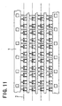
- FIG. 11 is a plan view of a conventional flat hoop frame;
- FIG. 12 is a schematic view illustrating different steps of a conventional production method for a semiconductor device;
- FIG. 13 is a detailed view of a resin filling metallic mold used in the production method illustrated in FIG. 12; and
- FIG. 14 is a side elevational view of an insulated semiconductor device produced by the production method illustrated in FIG. 12.
- FIG. 2 illustrates different steps of a production process for an insulated semiconductor device to which the present invention is applied, and FIG. 1 shows a flat hoop frame used for the production method illustrated in FIG. 2.
- Referring first to FIG. 1, the flat hoop frame is generally denoted at 1 and includes a large number of sets of leads having inner and outer lead portions arranged in a plurality of (four in FIG. 1) rows. The flat hoop frame 1 is formed such that, in each set of leads, inner lead portions extend farther than the position of a corresponding one of
resin filling centers 2 for the individual rows with a lead shaping amount determined taking a semiconductor pellet thickness and a bonding wire height into consideration so that the outer lead portions may be positioned at predetermined positions with respect to the semiconductor device of the set. - The flat hoop frame 1 supplied from a frame supply apparatus (refer to step A of FIG. 2) is successively subject, prior to the step of die bonding a semiconductor pellet to it, to simultaneous shaping of the
inner lead portions 3 thereof for the plurality of rows (in the lateral direction) at a plurality of pitches (in the longitudinal direction) by a lead shaping apparatus mounted on the frame supply apparatus or on a die bonding apparatus (refer to step B of FIG. 2). It is to be noted that, where the lead shaping step is performed prior to the die bonding step, the lead shaping apparatus may naturally be provided as a single machine. - Then, after die bonding of a semiconductor pellet to each island 10 (refer to step C of FIG. 2) and wire bonding (refer to step D of FIG. 2) are performed, resin is filled into only one of upper and lower metallic mold cavities by a resin filling apparatus so that the outer lead portions of the flat hoop frame may be positioned at predetermined positions with respect to the outer profiles of the semiconductor devices after the resin is filled (refer to step E of FIG. 2). Then, after the resin is filled, the
outer leads 17 are cut by a lead cutting apparatus (refer to step F of FIG. 2). - In the following, the production method for an insulated semiconductor device according to the embodiment of the present invention will be described in more detail.
- As seen in FIG. 1, the flat hoop frame 1 is formed such that the
inner lead portions 3 in each set of leads extend farther than the position of the correspondingresin filling center 2 taking a lead shaping amount into consideration. In particular, as seen from FIG. 4(A) which shows details of lead portions of the flat hoop frame 1, theinner lead portions 3 in each set of leads and theisland 10 extend farther than theresin filling center 2 by an amount corresponding to the lead shaping amount which is determined taking a semiconductor pellet thickness and a bonding wire height upon lead formation into consideration. - FIG. 6 illustrates details of the steps performed by the frame supply apparatus, lead shaping apparatus and die bonding apparatus. Referring to FIG. 6, the flat hoop frame 1 is fed from the
frame supply apparatus 4 to the lead shaping apparatus 6 mounted at a location of thedie bonding apparatus 5. - By the lead shaping apparatus 6 to which the flat hoop frame 1 is supplied, the
inner lead portions 3 of the flat hoop frame 1 are shaped downwardly into an L-shape simultaneously for the plurality of rows and the plurality of pitches by lead shapingpunches 7 and a die 8 as seen in FIGS. 7(A) and 7(B) which illustrate a manner of lead shaping. Thereafter, the flat hoop frame 1 is supplied via a buffer 9 to the diebonding apparatus 5. It is to be noted that FIG. 4(B) illustrates a manner in which theinner lead portions 3 are shaped downwardly into an L-shape by the lead shaping apparatus 6. - By the
die bonding apparatus 5, die bonding ofsemiconductor pellets 11 on theislands 10 of theinner lead portions 3 of the flat hoop frame 1 supplied thereto is performed (refer to step C of FIG. 2). After completion of the die bonding, the flat hoop frame 1 is supplied to a wire bonding apparatus via another buffer. - For the flat hoop frame 1 supplied to the wire bonding apparatus, pads of the
semiconductor pellets 11 and theinner lead portions 3 are bonded usingwires 18 by the wire bonding apparatus (refer to step E of FIG. 2 and also to FIG. 8(A)). After completion of the wire bonding, the flat hoop frame 1 is supplied to a resin filling apparatus via a further buffer. - The flat hoop frame 1 supplied to the resin filling apparatus is held between and pressurized by an upper
metallic mold 14 and a lowermetallic mold 15 as seen in FIG. 8(B), and then resin is filled only into lowermetallic mold cavities 16. Thereafter, the flat hoop frame 1 is accommodated into a frame take-up machine. A manner of a semiconductor device and outer leads of it after the resin is filled is shown in plan view in FIG. 3(A) and in sectional view taken along line A-A' of FIG. 3(A) in FIG. 3(B). As seen from FIGS. 3(A) and 3(B), the outer leads 17 of the semiconductor device filled with the resin are bent at an end face of the semiconductor device and then extend in the outward directions (leftward and rightward directions in FIGS. 3(A) and 3(B)) along the end face. - After taken up onto the frame take-up machine, the flat hoop frame 1 is solder plated by a solder plating apparatus. After the solder plating, the flat hoop frame 1 is supplied to and worked by a composite apparatus (refer to step F of FIG. 2) which includes a lead cutting apparatus, a selection apparatus, a printing apparatus and a taping apparatus, by which it is finally taken up by a predetermined amount onto a shipment reel. It is to be noted that the outer leads 17 are cut by the composite apparatus so that the outer leads 17 (foot portions) extends along the lower face of the
semiconductor device 20 and project by a predetermined amount outwardly from the lower face as seen in FIG. 5. - FIG. 9(A) shows details of lead portions of a flat hoop frame which is employed for a production method for an insulated semiconductor device according to another embodiment of the present invention, and FIG. 9(B) shows details of the lead portions after inner lead shaping is performed using the production method for an insulated semiconductor device of the second embodiment. Meanwhile, FIG. 9(C) shows details of lead portions of a conventional flat hop frame, and FIG. 9(D) shows details of the lead portions of the flat hop frame of FIG. 9(C) after inner lead shaping is performed using a conventional method. Further, FIGS. 10(A) and 10(B) show details of a resin filling metallic mold employed in the production method of the present embodiment.
- Referring to FIG. 9(A), in the flat hoop frame 1 which is used for the production method of the present embodiment,
inner lead portions 3 are formed, taking a lead shaping amount into consideration, such that they are elongated farther than the position of a correspondingresin filling center 2. - For the flat hoop frame 1, the
inner lead portions 3 are shaped upwardly into an L-shape simultaneously for a plurality of rows and a plurality of pitches by a lead shaping apparatus (refer to FIG. 9(B)). - In the present embodiment, in the resin filling step following the die bonding and wire bonding steps, resin is filled only into an upper
metallic mold cavity 24 of a resin filling metallic mold as seen in FIG. 10(B). Consequently, the lead shaping amount and length can be minimized. - Further, the production method of the present embodiment is advantageous in that, by boding
wires 18 obliquely in the wire bonding step, lead shaping (refer to FIG. 9(D) can be performed for the conventional flat hoop frame 1 (refer to FIG. 9(C)). - Having now fully described the invention, it will be apparent to one of ordinary skill in the art that many changes and modifications can be made thereto without departing from the spirit and scope of the invention as set forth herein.
Claims (6)
- A production method for an insulated semiconductor device, characterized in that it comprises the steps of:forming a flat hoop frame (1) having a plurality of rows of sets of leads such that inner lead portions (3) of the leads extend farther than corresponding resin filling centers (2) so that outer lead portions (17) of the leads may be positioned at predetermined positions with respect to outer profiles of semiconductor devices (20) after resin is filled and supplying the flat hoop frame (1) from a frame supply apparatus (4);shaping the inner lead portions (3) of the leads of the flat hoop frame (1) simultaneously for the plurality of rows and for a plurality of pitches by a lead shaping apparatus (6);performing die bonding of semiconductor pellets (11) and wire bonding for the flat hoop frame (1); andfilling, for each set of leads, resin into one of two cavities (16; 24) by a resin filling apparatus (13) so that the outer lead portions (17) of the leads of the flat hoop frame (1) may be positioned at the predetermined positions with respect to the outer profiles of the semiconductor devices (20) after the resin is filled.
- A production method for an insulated semiconductor device as set forth in claim 1, characterized in that the inner lead portions (3) of the leads of the flat hoop frame (1) are elongated farther than the positions of the resin filling centers (2) in accordance with the lead shaping amount determined taking a semiconductor pellet thickness and a bonding wire height into consideration.
- A production method for an insulated semiconductor device as set forth in claim 1, characterized in that shaping of the inner lead portions (3) of the leads of the flat hoop frame (1) supplied from said frame supply apparatus (4) is performed prior to the step of die bonding semiconductor pellets (11), and in the resin filling step following the die bonding step and the wire bonding step, the resin is filled into one of an upper metallic mold cavity (24) and a lower metallic mold cavity (16) for each set of leads.
- A production method for an insulated semiconductor device as set forth in claim 3, characterized in that the inner lead portions (3) of the leads of the flat hoop frame (1) extend by a predetermined additional length farther than the positions of the individual resin filling centers (2).
- A production method for an insulated semiconductor device as set forth in claim 3, characterized in that the inner lead portions (3) of the leads of the flat hoop frame (1) are worked into an L-shape at predetermined positions in the individual longitudinal directions in such a manner as to be positioned on the upper side or the lower side with respect to the outer lead portions (17) of the leads.
- A production method for an insulated semiconductor device as set forth in claim 3, characterized in that, in each of the semiconductor devices (20) filled with the resin, the outer lead portions (17) of the leads extend along an end face of the semiconductor device (20) and outwardly from the end face.
Applications Claiming Priority (2)
| Application Number | Priority Date | Filing Date | Title |
|---|---|---|---|
| JP8080777A JP2828016B2 (en) | 1996-03-08 | 1996-03-08 | Manufacturing method of insulated semiconductor device |
| JP80777/96 | 1996-03-08 |
Publications (2)
| Publication Number | Publication Date |
|---|---|
| EP0794560A2 true EP0794560A2 (en) | 1997-09-10 |
| EP0794560A3 EP0794560A3 (en) | 1998-03-18 |
Family
ID=13727878
Family Applications (1)
| Application Number | Title | Priority Date | Filing Date |
|---|---|---|---|
| EP97103714A Withdrawn EP0794560A3 (en) | 1996-03-08 | 1997-03-06 | Production method for insulated semiconductor device |
Country Status (4)
| Country | Link |
|---|---|
| US (1) | US5705431A (en) |
| EP (1) | EP0794560A3 (en) |
| JP (1) | JP2828016B2 (en) |
| KR (1) | KR100246694B1 (en) |
Families Citing this family (4)
| Publication number | Priority date | Publication date | Assignee | Title |
|---|---|---|---|---|
| JP2781783B2 (en) * | 1996-07-30 | 1998-07-30 | 山形日本電気株式会社 | Package for semiconductor device |
| JP3012816B2 (en) * | 1996-10-22 | 2000-02-28 | 松下電子工業株式会社 | Resin-sealed semiconductor device and method of manufacturing the same |
| EP1324386B1 (en) * | 2001-12-24 | 2011-06-15 | ABB Research Ltd. | Semiconductor module and method of manufacturing a semiconductor module |
| JP5771480B2 (en) * | 2011-08-31 | 2015-09-02 | 新電元工業株式会社 | Lead frame and method for manufacturing semiconductor device |
Citations (3)
| Publication number | Priority date | Publication date | Assignee | Title |
|---|---|---|---|---|
| FR1471243A (en) * | 1966-01-19 | 1967-03-03 | Radiotechnique | Enhancements to semiconductor devices embedded in a molded insulating protective coating |
| DE3421539A1 (en) * | 1984-06-08 | 1985-12-19 | Siemens AG, 1000 Berlin und 8000 München | Semiconductor component for SMD technology |
| US5508557A (en) * | 1992-10-09 | 1996-04-16 | Rohm Co., Ltd. | Surface mounting type diode |
Family Cites Families (8)
| Publication number | Priority date | Publication date | Assignee | Title |
|---|---|---|---|---|
| JPS5550648A (en) * | 1978-10-06 | 1980-04-12 | Mitsubishi Electric Corp | Resin sealing type semiconductor device |
| JPS6175553A (en) * | 1984-09-21 | 1986-04-17 | Hitachi Tobu Semiconductor Ltd | Electronic part |
| JPS62298146A (en) * | 1986-06-18 | 1987-12-25 | Hitachi Micro Comput Eng Ltd | Electronic device |
| US5202288A (en) * | 1990-06-01 | 1993-04-13 | Robert Bosch Gmbh | Method of manufacturing an electronic circuit component incorporating a heat sink |
| US5172214A (en) * | 1991-02-06 | 1992-12-15 | Motorola, Inc. | Leadless semiconductor device and method for making the same |
| EP0550013B1 (en) * | 1991-12-27 | 2000-07-26 | Fujitsu Limited | Semiconductor device and method of producing the same |
| US5436492A (en) * | 1992-06-23 | 1995-07-25 | Sony Corporation | Charge-coupled device image sensor |
| US5327008A (en) * | 1993-03-22 | 1994-07-05 | Motorola Inc. | Semiconductor device having universal low-stress die support and method for making the same |
-
1996
- 1996-03-08 JP JP8080777A patent/JP2828016B2/en not_active Expired - Fee Related
-
1997
- 1997-03-04 US US08/808,036 patent/US5705431A/en not_active Expired - Fee Related
- 1997-03-06 EP EP97103714A patent/EP0794560A3/en not_active Withdrawn
- 1997-03-08 KR KR1019970007861A patent/KR100246694B1/en not_active IP Right Cessation
Patent Citations (3)
| Publication number | Priority date | Publication date | Assignee | Title |
|---|---|---|---|---|
| FR1471243A (en) * | 1966-01-19 | 1967-03-03 | Radiotechnique | Enhancements to semiconductor devices embedded in a molded insulating protective coating |
| DE3421539A1 (en) * | 1984-06-08 | 1985-12-19 | Siemens AG, 1000 Berlin und 8000 München | Semiconductor component for SMD technology |
| US5508557A (en) * | 1992-10-09 | 1996-04-16 | Rohm Co., Ltd. | Surface mounting type diode |
Non-Patent Citations (3)
| Title |
|---|
| PATENT ABSTRACTS OF JAPAN vol. 004, no. 083 (E-015), 14 June 1980 & JP 55 050648 A (MITSUBISHI ELECTRIC CORP), 12 April 1980, * |
| PATENT ABSTRACTS OF JAPAN vol. 010, no. 244 (E-430), 22 August 1986 & JP 61 075553 A (HITACHI TOBU SEMICONDUCTOR LTD;OTHERS: 01), 17 April 1986, * |
| PATENT ABSTRACTS OF JAPAN vol. 012, no. 196 (E-618), 7 June 1988 -& JP 62 298146 A (HITACHI MICRO COMPUT ENG LTD;OTHERS: 01), 25 December 1987, * |
Also Published As
| Publication number | Publication date |
|---|---|
| JPH09246305A (en) | 1997-09-19 |
| JP2828016B2 (en) | 1998-11-25 |
| KR100246694B1 (en) | 2000-03-15 |
| EP0794560A3 (en) | 1998-03-18 |
| KR970067813A (en) | 1997-10-13 |
| US5705431A (en) | 1998-01-06 |
Similar Documents
| Publication | Publication Date | Title |
|---|---|---|
| EP0397320A2 (en) | Encapsulated integrated circuit with lead frame | |
| JP2003209216A (en) | Lead frame, resin sealed die and method for manufacturing semiconductor device using them | |
| US6271586B1 (en) | Integrated circuit chip and method for fabricating the same | |
| US5384286A (en) | Process for encapsulating a semiconductor chip, leadframe and heatsink | |
| JP5448727B2 (en) | Semiconductor device and manufacturing method thereof | |
| US5705431A (en) | Production method for insulated semiconductor device | |
| US6946729B2 (en) | Wafer level package structure with a heat slug | |
| JPH06291234A (en) | Semiconductor device lead frame and semiconductor device provided therewith | |
| US6303983B1 (en) | Apparatus for manufacturing resin-encapsulated semiconductor devices | |
| KR100334699B1 (en) | Wire bonding method | |
| US10937728B2 (en) | Preformed lead frame and lead frame package made from the same | |
| JPS63187657A (en) | Manufacture of semiconductor device | |
| JP3028167B2 (en) | Lead frame manufacturing method and lead frame manufacturing apparatus | |
| US6512286B1 (en) | Semiconductor package with no void in encapsulant and method for fabricating the same | |
| JPH08172153A (en) | Method of lead forming for semiconductor device and metal mold therefor | |
| JPH0653399A (en) | Resin-sealed semiconductor device | |
| KR100571558B1 (en) | How to prevent burrs of window slit during punching process of printed circuit board | |
| JPH0738036A (en) | Manufacture of semiconductor device | |
| JP2743876B2 (en) | Method for manufacturing semiconductor device | |
| JPH1126669A (en) | Tie bar cutting die | |
| JPH0828449B2 (en) | Lead frame manufacturing method | |
| KR100285917B1 (en) | semiconductor package strip and forming method thereof | |
| KR950008850B1 (en) | Semiconductor device and manufacture method | |
| JPH07321135A (en) | Tie bar cut-off device | |
| JPH0864737A (en) | Resin-sealed semiconductor device and lead frame |
Legal Events
| Date | Code | Title | Description |
|---|---|---|---|
| PUAI | Public reference made under article 153(3) epc to a published international application that has entered the european phase |
Free format text: ORIGINAL CODE: 0009012 |
|
| AK | Designated contracting states |
Kind code of ref document: A2 Designated state(s): DE FR GB |
|
| PUAL | Search report despatched |
Free format text: ORIGINAL CODE: 0009013 |
|
| AK | Designated contracting states |
Kind code of ref document: A3 Designated state(s): DE FR GB |
|
| 17P | Request for examination filed |
Effective date: 19980629 |
|
| RAP1 | Party data changed (applicant data changed or rights of an application transferred) |
Owner name: NEC ELECTRONICS CORPORATION |
|
| 17Q | First examination report despatched |
Effective date: 20030417 |
|
| STAA | Information on the status of an ep patent application or granted ep patent |
Free format text: STATUS: THE APPLICATION IS DEEMED TO BE WITHDRAWN |
|
| 18D | Application deemed to be withdrawn |
Effective date: 20051220 |