EP0800308B1 - Solid state color imaging device - Google Patents
Solid state color imaging device Download PDFInfo
- Publication number
- EP0800308B1 EP0800308B1 EP97109659A EP97109659A EP0800308B1 EP 0800308 B1 EP0800308 B1 EP 0800308B1 EP 97109659 A EP97109659 A EP 97109659A EP 97109659 A EP97109659 A EP 97109659A EP 0800308 B1 EP0800308 B1 EP 0800308B1
- Authority
- EP
- European Patent Office
- Prior art keywords
- color
- sensor
- sensors
- signal
- signal charges
- Prior art date
- Legal status (The legal status is an assumption and is not a legal conclusion. Google has not performed a legal analysis and makes no representation as to the accuracy of the status listed.)
- Expired - Lifetime
Links
Images


Classifications
-
- H—ELECTRICITY
- H04—ELECTRIC COMMUNICATION TECHNIQUE
- H04N—PICTORIAL COMMUNICATION, e.g. TELEVISION
- H04N25/00—Circuitry of solid-state image sensors [SSIS]; Control thereof
- H04N25/60—Noise processing, e.g. detecting, correcting, reducing or removing noise
- H04N25/63—Noise processing, e.g. detecting, correcting, reducing or removing noise applied to dark current
-
- H—ELECTRICITY
- H04—ELECTRIC COMMUNICATION TECHNIQUE
- H04N—PICTORIAL COMMUNICATION, e.g. TELEVISION
- H04N1/00—Scanning, transmission or reproduction of documents or the like, e.g. facsimile transmission; Details thereof
- H04N1/46—Colour picture communication systems
- H04N1/48—Picture signal generators
- H04N1/486—Picture signal generators with separate detectors, each detector being used for one specific colour component
-
- H—ELECTRICITY
- H04—ELECTRIC COMMUNICATION TECHNIQUE
- H04N—PICTORIAL COMMUNICATION, e.g. TELEVISION
- H04N23/00—Cameras or camera modules comprising electronic image sensors; Control thereof
- H04N23/80—Camera processing pipelines; Components thereof
- H04N23/84—Camera processing pipelines; Components thereof for processing colour signals
-
- H—ELECTRICITY
- H04—ELECTRIC COMMUNICATION TECHNIQUE
- H04N—PICTORIAL COMMUNICATION, e.g. TELEVISION
- H04N25/00—Circuitry of solid-state image sensors [SSIS]; Control thereof
- H04N25/60—Noise processing, e.g. detecting, correcting, reducing or removing noise
- H04N25/62—Detection or reduction of noise due to excess charges produced by the exposure, e.g. smear, blooming, ghost image, crosstalk or leakage between pixels
- H04N25/621—Detection or reduction of noise due to excess charges produced by the exposure, e.g. smear, blooming, ghost image, crosstalk or leakage between pixels for the control of blooming
-
- H—ELECTRICITY
- H04—ELECTRIC COMMUNICATION TECHNIQUE
- H04N—PICTORIAL COMMUNICATION, e.g. TELEVISION
- H04N25/00—Circuitry of solid-state image sensors [SSIS]; Control thereof
- H04N25/70—SSIS architectures; Circuits associated therewith
-
- H—ELECTRICITY
- H04—ELECTRIC COMMUNICATION TECHNIQUE
- H04N—PICTORIAL COMMUNICATION, e.g. TELEVISION
- H04N25/00—Circuitry of solid-state image sensors [SSIS]; Control thereof
- H04N25/70—SSIS architectures; Circuits associated therewith
- H04N25/701—Line sensors
-
- H—ELECTRICITY
- H04—ELECTRIC COMMUNICATION TECHNIQUE
- H04N—PICTORIAL COMMUNICATION, e.g. TELEVISION
- H04N25/00—Circuitry of solid-state image sensors [SSIS]; Control thereof
- H04N25/70—SSIS architectures; Circuits associated therewith
- H04N25/71—Charge-coupled device [CCD] sensors; Charge-transfer registers specially adapted for CCD sensors
- H04N25/713—Transfer or readout registers; Split readout registers or multiple readout registers
-
- H—ELECTRICITY
- H04—ELECTRIC COMMUNICATION TECHNIQUE
- H04N—PICTORIAL COMMUNICATION, e.g. TELEVISION
- H04N25/00—Circuitry of solid-state image sensors [SSIS]; Control thereof
- H04N25/70—SSIS architectures; Circuits associated therewith
- H04N25/71—Charge-coupled device [CCD] sensors; Charge-transfer registers specially adapted for CCD sensors
- H04N25/75—Circuitry for providing, modifying or processing image signals from the pixel array
-
- H—ELECTRICITY
- H04—ELECTRIC COMMUNICATION TECHNIQUE
- H04N—PICTORIAL COMMUNICATION, e.g. TELEVISION
- H04N2209/00—Details of colour television systems
- H04N2209/04—Picture signal generators
- H04N2209/041—Picture signal generators using solid-state devices
- H04N2209/048—Picture signal generators using solid-state devices having several pick-up sensors
- H04N2209/049—Picture signal generators using solid-state devices having several pick-up sensors having three pick-up sensors
Definitions
- the present invention generally relates to a solid state color imaging device, color linear sensors and, more particularly, to a color linear sensor having a dot-sequential sensor array in which photo sensors of three colors such as R (red), G (green), B (blue) or the like are sequentially arranged at the unit of pixels in a one-dimensional fashion.
- Linear image sensors (hereinafter simply referred to as “linear sensors”) have advantages such that they are small in size and low in electric power consumption. Hence, the linear image sensors are utilized in a wide variety of fields such as copy, facsimile image transmission, optical character recognition (OCR), pattern recognition, measurement and so on. As color copies are popularizing recently, color linear sensors are often utilized.
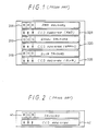
- Fig. 1 of the accompanying drawings shows a structure of a conventional color linear sensor of R, G, B line-sequential output type having three sensor arrays.
- this type of color linear sensor comprises three sensor arrays 31R, 31G, 31B for three colors and transfer registers 32R, 32G, 32B disposed relative to the above sensor arrays 31R, 31G, 31B to thereby output signal charges of one line for every color in a line-sequential fashion.
- Fig. 2 of the accompanying drawings shows a structure of another example of a conventional color linear sensor.
- this conventional color linear sensor is what might be called an R, G, B dot-sequential output type and includes a single sensor array 41 composed of R, G, B sensors arranged sequentially at the unit of pixels in a one-dimensional fashion and a single transfer register 42 opposed to the sensor array 41, thereby to output signal charges of respective pixels of one line simultaneously in a dot-sequential manner.
- the above color linear sensor of line-sequential output type includes the three sensor arrays 31R, 31G, 31B so that, when these sensor arrays 31R, 31G, 31B scan an object upon copying or the like, they are displaced from each other in position, which needs many memories for correcting such displacement. Furthermore, the above color linear sensor of line-sequential type needs three output pins (terminals) corresponding to three colors, R, G, B, which needs extra circuits such as an analog-to-digital (A/D) converter or the like to effect the signal processing in the outside. There is then the disadvantage such that an external circuit becomes complicated in configuration.
- the color linear sensor of dot-sequential output type having the single sensor array needs only a single output pin, which needs a single signal processing system.
- the prior-art color linear sensor is of the dot-sequential output type, sensors of different colors are repeatedly arranged, i.e., a green signal component is output after a red signal component is output, a blue signal component is output after the green signal component is output and the next red signal component is output after the blue signal component is output, etc.
- the signal component of the adjacent sensor section is mixed into the signal component of the adjacent sensor section. This phenomenon will hereinafter be referred to as "color mixture”.
- this mixed signal component appears as a color mixture on a picture after signal charges are transferred and deteriorated by the transfer register 42.
- the color mixture in the sensor section is eliminated as much as possible. Therefore, in the manufacturing process of color linear sensors, a degree with which the color mixture occurred in the sensor section must be measured and respective sections of the color linear sensor must be adjusted in accordance with the measured degree of the color mixture.
- color imaging devices comprising a linear sensor array are disclosed in IEEE 1991 International Conference on Consumer Electronics, 5 June 1991, Rosemont, Illinois, pages 150-151.
- Another object of the present invention is to provide a color linear sensor in which sensor sections can be prevented from being displaced in position.
- Still another object of the present invention is to provide a color linear sensor in which an external circuit can be simplified in configuration.
- a further object of the present invention is to provide a color linear sensor in which a color mixture due to a deterioration of signal charges after the signal charges are transferred by a transfer register can be avoided.
- the present invention provides a solid state color imaging device as specified in claim 1.
- a solid state color imaging device comprises a sensor array constituted by a linear array of first color sensors, second color sensors and third color sensors, the first, second and third color sensors being adopted for converting the light received by way of different color transmitting filters into signal charges, an optical black area including a plurality of light shielded sensors, a standard sensor formed in the optical black area, the standard sensor being adopted for converting the light received by way of a color transmitting filter which has a specific color selected among the different colors into standard signal charges with no other color mixed, and horizontal shift register for transferring the signal charges generated in the first, second and third color sensors and the standard signal charges generated in the standard sensor.
- FIG. 3 of the accompanying drawings shows a structure of a color linear sensor according to an embodiment of the present invention.
- a dot-sequential sensor array 1 comprises photo sensors 1R, 1G, 1B of three colors R, G, B each having a corresponding color filter (not shown) sequentially and repeatedly arranged at the unit of pixels in a one-dimensional fashion.
- the dot-sequential sensor array 1 is divided to provide an effective pixel region 2 which photoelectrically converts an incident light from the outside by the respective photo sensors 1R, 1G, 1B to obtain an image information and a reference pixel region 3 known as an optical black (OPB) region for detecting a reference level, e.g., black level (0 level) of an image information.
- OOB optical black
- the reference pixel region 3 can receive a light of only one pixel e.g., red pixel (R).
- Signal charges stored in the respective photo sensors of the dot-sequential sensor array 1 are simultaneously read out to a CCD (charge coupled device) register 5 as information of one line by a read-out gate (ROG) 4 composed of gate group disposed at every sensor.
- the CCD register 5 operates to sequentially transfer signal charges, read-out from the dot-sequential sensor array 1 by the read-out gate 4, in response to two-phase pulses ⁇ 1 , ⁇ 2 to an output terminal (left-hand side of FIG. 3).
- a charge detecting section 6 which detects and converts a transferred signal charge into an electrical signal. This electrical signal is developed at the output terminal 7 as an image signal.
- the image signal developed at the output terminal 7 is supplied to sample and hold circuits 8 and 9.
- the sample and hold circuits 8 and 9 operate to hold the signal level of the image signal in synchronism with sampling pulses SP1, SP2 that are generated from a timing generator 10 at different timings.
- Hold outputs from the sample and hold circuits 8, 9 are supplied to a differential amplifier 11, in which they are processed to provide a level difference therebetween.
- a voltmeter 13, for example, is connected between an output terminal 12 of the differential amplifier 11 and the ground.
- the timing generator 10 operates to generate the sampling pulse SP1 at timing at which a signal charge of a certain R sensor 1 ⁇ in the effective pixel region 2 of the sensor array 1 is output and the sampling pulse SP2 at timing at which a signal charge of a certain operative R sensor 2 ⁇ in the reference pixel region 3 is output. Further, the timing generator 10 generates a variety of timing signals, such as a gate pulse ⁇ GP used to open and/or close the read-out gate 4, the two-phase transfer clocks ⁇ 1 , ⁇ 2 or the like.
- the timing generator 10 At timings 1 ⁇ and 2 ⁇ , the timing generator 10 generates the sampling pulses SP1 and SP2, whereby the voltage levels of the waveforms 1 ⁇ and 2 ⁇ are sampled and held by the sample and hold circuits 8 and 9. Then, the differential amplifier 11 calculates a level difference ⁇ V between the waveforms 1 ⁇ and 2 ⁇ and this level difference ⁇ V is indicated by the voltmeter 13.
- the operative R (red) sensor 2 ⁇ in the reference pixel region 3 can be protected from being affected by the color mixture because the adjacent B (blue) and G (green) sensors are light-shielded sensors. Consequently, the difference ⁇ V of the voltage level of the waveform 1 ⁇ relative to the voltage level of the waveform 2 ⁇ shows a degree of the color mixture of the R sensor in the effective pixel region 2 ⁇ and a degree of the color mixture of the respective sensors.
- Color mixture may occur due to the following two cases (1) and (2): In any cases, the color mixture does not occur in the operative R sensor in the reference pixel region 3, while the color mixture occurs only in the R sensor 1 ⁇ in the effective pixel region 2.
- the degree of color mixture occurred due to the above causes can be measured as the level difference ⁇ V by the color linear sensor of this embodiment. Accordingly, if the position of color filters is adjusted and the pattern of the sensor section is optimized such that the level difference ⁇ V, i.e., the color mixture is minimized in the manufacturing process of the color linear sensor, then it becomes possible to provide a color linear sensor which has little color mixture.
- the operative sensor is not limited to the R sensor and might be sensors of other colors, i.e., G and B sensors. In short, it is sufficient that a level difference between the signal output of the sensor operative in the reference pixel region 3 and the signal output of the sensor of the same color as that of the R sensor in the effective pixel region 2 can be measured.
- the circuit configuration is not limited thereto and any circuit configuration becomes possible insofar as it can detect the level difference ⁇ V.
- the color linear sensor having the dot-sequential sensor array is arranged such that only one pixel of a predetermined color in the reference pixel region is allowed to receive an incident light and that a level difference between the signal output of this pixel and the signal output of the pixel of the same color as that of this pixel in the effective pixel region is calculated, the color mixture can be prevented from occurring in the operative pixel in the reference pixel region. Therefore, a degree with which the color mixture occurs in the sensor section in the effective pixel region can be accurately measured by the simple arrangement.
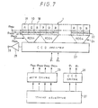
- FIG. 7 of the accompanying drawings shows a structure of a further color linear sensor.
- the three photo sensors 1R, 1G, 1B having color filters corresponding to R (red), G (green) and B (blue), for example, are sequentially arranged at the unit of pixels in a one-dimensional manner to construct the sensor array 1.
- Signal charges stored in the respective photo sensors forming the sensor array 1 are read out at the unit of pixels by a first read-out gate 22 which is composed of gate groups (ROG1, ROG2 and ROG3) disposed at every sensor.
- a single CCD register 23 is disposed as a transfer register for transferring signal charges read out from the sensor array 1.
- the CCD register 23 has a bit number of 1/3 of pixel number of the sensor array 1.
- a second read-out gate (ROG4) 24 for every adjacent photo sensors 1R, 1G, 1B of three colors in the sensor array 1.
- the second read-out gate 24 operates to supply signal charges of three pixel amounts sequentially read-out by the first read-out gate 22 to one bit of the CCD register 23.
- the CCD register 23 sequentially transfers signal charges, sequentially read-out from the sensor array 1 at the unit of pixels by the first and second read-out gates 22, 24, to an output terminal (left-hand side of FIG. 7) in response to the two-phase pulses ⁇ 1 , ⁇ 2 .
- a charge detecting section 25 for detecting and converting a signal charge transferred into an electrical signal is connected to the output terminal of the CCD register 23. Then, this electrical signal is developed at a single output terminal (pin) 26 and then fed to an external circuit (not shown).
- a timing generator 27 is adapted to generate at proper timings the transfer clocks ⁇ 1 , ⁇ 2 that are used to drive the CCD register 23 in a two-phase fashion and gate clocks ⁇ R O G 1 through ⁇ R O G 4 that are used to open and/or close the first and second read-out gates 22, 24.
- the two-phase transfer clocks ⁇ 1 , ⁇ 2 are applied to the CCD register 23 through a CCD driver 28 and the gate clocks ⁇ R O G 1 through ⁇ R O G 4 are applied to the first and second read-out gates 22, 24 through a gate driver 29.
- the gate clocks ⁇ R O G 1 and ⁇ R O G 4 go to high "H” level, thereby tuning on the ROG1 of the first read-out gate 22 and the second read-out gate (ROG4) 24. Also, the gate clocks ⁇ R O G 2 , ⁇ R O G 3 go to low "L” level, thereby turning off the ROG2, ROG3 of the first read-out gate 22. Thus, only the signal charges stored in the R (red) photo sensor 1R are read out to the CCD register 23 and transferred by the CCD register 23. At this timing point, signal charges of one line of R (red) are read out.
- the gate clocks ⁇ R O G 2 , ⁇ R O G 4 go to high "H” level, thereby turning on ROG2, ROG4 of the first read-out gate 22. Also, the gate clocks ⁇ R O G 1 , ⁇ R O G 3 go to low "L” level, thereby turning off the ROG1, ROG3 of the first read-out gate 22.
- the signal charges stored in the G (green) photo sensor 1G are read out to the CCD register 23 and transferred by the CCD register 23. At this timing point, the signal charges of one line of G (green) are read out after one line of R (red).
- the gate clocks ⁇ ROG3 , ⁇ ROG4 go to high "H” level, thereby turning on the ROG3, ROG4 of the first read-out gate 22. Also, the gate clocks ⁇ ROG1 , ⁇ ROG2 go to low "L” level, thereby turning off the ROG1, ROG2 of the first read-out gate 22. Consequently, only the signal charges stored in the B (blue) photo sensor 1B are read out to the CCD register 23 and transferred by the CCD register 23. At that time point, signal charges of each line of R, G, B are read out.
- the color linear sensor of the present invention since the color linear sensor of the present invention has the dot-sequential sensor array, the sensors can be protected from being positionally displaced unlike the color linear sensor of line-sequential output type having three sensor arrays.
- the color linear sensor of the present invention needs only one output pin (terminal), which can simplify the configuration of the external circuit. Further, since signal charges are output in a line-sequential fashion, signal charges deteriorated by the transfer operation by the CCD register 23 can be prevented from appearing on the picture as the color mixture.
- the read-out gate for reading out signal charges from the sensor array 1 is formed as a two-stage configuration composed of the first and second read-out gates 22, 24, the bit number of the CCD register 23 can be reduced to 1/3 of the pixel number of the sensor array 1 and the transfer frequency of the CCD register 23 can be decreased to 1/3, which can reduce an electric power consumption.
- the read-out gate is formed as the two-stage configuration to output signal charge in a line-sequential fashion as described above, even if the second read-out gate 24 is omitted, signal charges can be output in a line-sequential manner by the dot-sequential sensor array by properly controlling the drive timing of the first read-out gate 22.
- the bit number of the CCD register 23 becomes the same as the number of pixels forming the sensor array 1 so that the frequency three times as high as that described above is needed as the transfer frequency of the CCD register 23.
- the color linear sensor having the dot-sequential sensor array is arranged so as to output signal charges of one line at every color in a line-sequential fashion. Because the color linear sensor of the present invention includes the dot-sequential sensor array, the sensors can be prevented from being displaced in position unlike the color linear sensor of the line-sequential output type. Further, the color linear sensor of the present invention needs only one output pin (terminal), which can simplify the configuration of the external circuit. Also, since the color linear sensor of the present invention outputs signal charges in a line-sequential fashion, the color mixture caused by the deterioration of signal charges transferred by the transfer register can be avoided.
- the read-out gate is formed of two-stage read-out gates, the bit number of the transfer register can be reduced to 1/3 of the pixel number of the sensor array. Hence, the transfer frequency of the transfer register can be reduced to 1/3, which can reduce an electric power consumption.
Description
- The present invention generally relates to a solid state color imaging device, color linear sensors and, more particularly, to a color linear sensor having a dot-sequential sensor array in which photo sensors of three colors such as R (red), G (green), B (blue) or the like are sequentially arranged at the unit of pixels in a one-dimensional fashion.
- Linear image sensors (hereinafter simply referred to as "linear sensors") have advantages such that they are small in size and low in electric power consumption. Hence, the linear image sensors are utilized in a wide variety of fields such as copy, facsimile image transmission, optical character recognition (OCR), pattern recognition, measurement and so on. As color copies are popularizing recently, color linear sensors are often utilized.
- Fig. 1 of the accompanying drawings shows a structure of a conventional color linear sensor of R, G, B line-sequential output type having three sensor arrays.
- As shown in Fig. 1, this type of color linear sensor comprises three
sensor arrays transfer registers above sensor arrays - Fig. 2 of the accompanying drawings shows a structure of another example of a conventional color linear sensor.
- As shown in Fig. 2, this conventional color linear sensor is what might be called an R, G, B dot-sequential output type and includes a
single sensor array 41 composed of R, G, B sensors arranged sequentially at the unit of pixels in a one-dimensional fashion and asingle transfer register 42 opposed to thesensor array 41, thereby to output signal charges of respective pixels of one line simultaneously in a dot-sequential manner. - The above color linear sensor of line-sequential output type includes the three
sensor arrays sensor arrays - On the other hand, the color linear sensor of dot-sequential output type having the single sensor array needs only a single output pin, which needs a single signal processing system. However, since the prior-art color linear sensor is of the dot-sequential output type, sensors of different colors are repeatedly arranged, i.e., a green signal component is output after a red signal component is output, a blue signal component is output after the green signal component is output and the next red signal component is output after the blue signal component is output, etc. As a result, the signal component of the adjacent sensor section is mixed into the signal component of the adjacent sensor section. This phenomenon will hereinafter be referred to as "color mixture". That is, this mixed signal component appears as a color mixture on a picture after signal charges are transferred and deteriorated by the
transfer register 42. Thus, it is desirable that the color mixture in the sensor section is eliminated as much as possible. Therefore, in the manufacturing process of color linear sensors, a degree with which the color mixture occurred in the sensor section must be measured and respective sections of the color linear sensor must be adjusted in accordance with the measured degree of the color mixture. - Examples of color imaging devices comprising a linear sensor array are disclosed in IEEE 1991 International Conference on Consumer Electronics, 5 June 1991, Rosemont, Illinois, pages 150-151.
- Accordingly, it is an object of the present invention to provide an improved color linear sensor in which the aforesaid shortcomings and disadvantages encountered with the prior art can be eliminated.
- More specifically, it is an object of the present invention to provide a color linear sensor of simple structure which can accurately measure a degree of color mixture.
- Another object of the present invention is to provide a color linear sensor in which sensor sections can be prevented from being displaced in position.
- Still another object of the present invention is to provide a color linear sensor in which an external circuit can be simplified in configuration.
- A further object of the present invention is to provide a color linear sensor in which a color mixture due to a deterioration of signal charges after the signal charges are transferred by a transfer register can be avoided.
- To solve this object the present invention provides a solid state color imaging device as specified in
claim 1. - Preferred embodiments of the invention are defined by the dependent claim.
- In accordance with an aspect of the present invention, a solid state color imaging device comprises a sensor array constituted by a linear array of first color sensors, second color sensors and third color sensors, the first, second and third color sensors being adopted for converting the light received by way of different color transmitting filters into signal charges, an optical black area including a plurality of light shielded sensors, a standard sensor formed in the optical black area, the standard sensor being adopted for converting the light received by way of a color transmitting filter which has a specific color selected among the different colors into standard signal charges with no other color mixed, and horizontal shift register for transferring the signal charges generated in the first, second and third color sensors and the standard signal charges generated in the standard sensor.
- The above and other objects, features and advantages of the present invention will become apparent from the following detailed description of an illustrative embodiment thereof to be read in conjunction with the accompanying drawings.
-
- FIG. 1 is a diagram of a structure of an example of a color linear sensor of a line-sequential output type that includes three dot-sequential sensor arrays according to the prior art;
- FIG. 2 is a diagram of a structure of another example of a color linear sensor of a dot-sequential output type that includes a single dot-sequential sensor array according to the prior art;
- FIG. 3 is a diagram of a structure of a color linear sensor according to an embodiment of the present invention;
- FIG. 4 is a diagram of a waveform of an image signal of a red (R) component;
- FIG. 5 is a fragmentary cross-sectional view used to explain a cause of the occurrence of a color mixture;
- FIG. 6 is a fragmentary cross-sectional view used to explain another cause of the occurrence of a color mixture;
- FIG. 7 is a diagram of a structure of a color linear sensor ; and
- FIG. 8 is a timing chart used to explain operation of the color linear sensor of Fig. 7.
-
- The present invention will now be described in detail with reference to the drawings.
- FIG. 3 of the accompanying drawings shows a structure of a color linear sensor according to an embodiment of the present invention.
- Referring to FIG. 3, a dot-
sequential sensor array 1 comprisesphoto sensors sequential sensor array 1 is divided to provide aneffective pixel region 2 which photoelectrically converts an incident light from the outside by therespective photo sensors reference pixel region 3 known as an optical black (OPB) region for detecting a reference level, e.g., black level (0 level) of an image information. Then, thereference pixel region 3 can receive a light of only one pixel e.g., red pixel (R). - Signal charges stored in the respective photo sensors of the dot-
sequential sensor array 1 are simultaneously read out to a CCD (charge coupled device)register 5 as information of one line by a read-out gate (ROG) 4 composed of gate group disposed at every sensor. TheCCD register 5 operates to sequentially transfer signal charges, read-out from the dot-sequential sensor array 1 by the read-outgate 4, in response to two-phase pulses 1, 2 to an output terminal (left-hand side of FIG. 3). At the output terminal of theCCD register 5, there is connected acharge detecting section 6 which detects and converts a transferred signal charge into an electrical signal. This electrical signal is developed at theoutput terminal 7 as an image signal. - The image signal developed at the
output terminal 7 is supplied to sample and holdcircuits 8 and 9. The sample and holdcircuits 8 and 9 operate to hold the signal level of the image signal in synchronism with sampling pulses SP1, SP2 that are generated from atiming generator 10 at different timings. Hold outputs from the sample and holdcircuits 8, 9 are supplied to adifferential amplifier 11, in which they are processed to provide a level difference therebetween. Avoltmeter 13, for example, is connected between anoutput terminal 12 of thedifferential amplifier 11 and the ground. - The
timing generator 10 operates to generate the sampling pulse SP1 at timing at which a signal charge of acertain R sensor 1 ○ in theeffective pixel region 2 of thesensor array 1 is output and the sampling pulse SP2 at timing at which a signal charge of a certainoperative R sensor 2 ○ in thereference pixel region 3 is output. Further, thetiming generator 10 generates a variety of timing signals, such as a gate pulse GP used to open and/or close the read-outgate 4, the two-phase transfer clocks 1 , 2 or the like. - Operation of the color linear sensor according to the embodiment of the present invention will be described below.
- Signal charges of the respective sensors in the
sensor array 1 are read-out to theCCD register 5 by the read-outgate 4 and sequentially transferred to the output terminal side by theCCD register 5, thereby the image signal of one line being developed at theoutput terminal 7. Study of only the R (red) signal component of R, G, B signal components reveals that an output waveform of the R signal component is presented as shown in FIG. 4. In the waveform diagram of FIG. 4,waveforms 1 ○ and 2 ○ correspond to the red (R)sensor 1 ○ in theeffective pixel region 2 and the operativered sensor 2 ○ in thereference pixel region 3. - At
timings 1 ○ and 2 ○, thetiming generator 10 generates the sampling pulses SP1 and SP2, whereby the voltage levels of thewaveforms 1 ○ and 2 ○ are sampled and held by the sample and holdcircuits 8 and 9. Then, thedifferential amplifier 11 calculates a level difference ΔV between thewaveforms 1 ○ and 2 ○ and this level difference ΔV is indicated by thevoltmeter 13. - The operative R (red)
sensor 2 ○ in thereference pixel region 3 can be protected from being affected by the color mixture because the adjacent B (blue) and G (green) sensors are light-shielded sensors. Consequently, the difference ΔV of the voltage level of thewaveform 1 ○ relative to the voltage level of thewaveform 2 ○ shows a degree of the color mixture of the R sensor in theeffective pixel region 2 ○ and a degree of the color mixture of the respective sensors. - Color mixture may occur due to the following two cases (1) and (2): In any cases, the color mixture does not occur in the operative R sensor in the
reference pixel region 3, while the color mixture occurs only in theR sensor 1 ○ in theeffective pixel region 2. - The case (1): As shown in FIG. 5, light beams traveling through the color filters (B filter and G filter) on the adjacent B and G sensors are introduced into the R sensor which should be protected from the incident light, thereby causing the color mixture.
- The case (2): As shown in FIG. 6, an electron photoelectrically-converted near an Si interface of sensors by an incident light beam from the adjacent B and G sensors enters the
R sensor 1 ○, thereby causing the color mixture. - The degree of color mixture occurred due to the above causes can be measured as the level difference ΔV by the color linear sensor of this embodiment. Accordingly, if the position of color filters is adjusted and the pattern of the sensor section is optimized such that the level difference ΔV, i.e., the color mixture is minimized in the manufacturing process of the color linear sensor, then it becomes possible to provide a color linear sensor which has little color mixture.
- While only the R sensor in the
reference pixel region 3 is designed so as to receive an incident light as described above, the operative sensor is not limited to the R sensor and might be sensors of other colors, i.e., G and B sensors. In short, it is sufficient that a level difference between the signal output of the sensor operative in thereference pixel region 3 and the signal output of the sensor of the same color as that of the R sensor in theeffective pixel region 2 can be measured. - While the level difference ΔV of the voltage level of the
waveform 1 ○ relative to the voltage level of thewaveform 2 ○ is detected by the circuit configuration composed of the sample and holdcircuits 8, 9 and thedifferential amplifier 11, the circuit configuration is not limited thereto and any circuit configuration becomes possible insofar as it can detect the level difference ΔV. - As described above, according to the present invention, since the color linear sensor having the dot-sequential sensor array is arranged such that only one pixel of a predetermined color in the reference pixel region is allowed to receive an incident light and that a level difference between the signal output of this pixel and the signal output of the pixel of the same color as that of this pixel in the effective pixel region is calculated, the color mixture can be prevented from occurring in the operative pixel in the reference pixel region. Therefore, a degree with which the color mixture occurs in the sensor section in the effective pixel region can be accurately measured by the simple arrangement.
- FIG. 7 of the accompanying drawings shows a structure of a further color linear sensor.
- As shown in FIG. 7, the three
photo sensors sensor array 1. Signal charges stored in the respective photo sensors forming thesensor array 1 are read out at the unit of pixels by a first read-out gate 22 which is composed of gate groups (ROG1, ROG2 and ROG3) disposed at every sensor. - A
single CCD register 23 is disposed as a transfer register for transferring signal charges read out from thesensor array 1. TheCCD register 23 has a bit number of 1/3 of pixel number of thesensor array 1. Between the first read-out gate 22 and theCCD register 23, there is disposed a second read-out gate (ROG4) 24 for everyadjacent photo sensors sensor array 1. The second read-out gate 24 operates to supply signal charges of three pixel amounts sequentially read-out by the first read-out gate 22 to one bit of theCCD register 23. - Then, the CCD register 23 sequentially transfers signal charges, sequentially read-out from the
sensor array 1 at the unit of pixels by the first and second read-outgates charge detecting section 25 for detecting and converting a signal charge transferred into an electrical signal is connected to the output terminal of theCCD register 23. Then, this electrical signal is developed at a single output terminal (pin) 26 and then fed to an external circuit (not shown). - A
timing generator 27 is adapted to generate at proper timings the transfer clocks 1, 2 that are used to drive theCCD register 23 in a two-phase fashion and gate clocks R O G 1 through R O G 4 that are used to open and/or close the first and second read-outgates CCD register 23 through aCCD driver 28 and the gate clocks R O G 1 through R O G 4 are applied to the first and second read-outgates gate driver 29. - Operation of the color linear sensor arranged as described above will be described with reference to a timing chart forming FIG. 8.
- Initially, at timing point t = t0, the gate clocks R O G 1 and R O G 4 go to high "H" level, thereby tuning on the ROG1 of the first read-
out gate 22 and the second read-out gate (ROG4) 24. Also, the gate clocks R O G 2 , R O G 3 go to low "L" level, thereby turning off the ROG2, ROG3 of the first read-out gate 22. Thus, only the signal charges stored in the R (red)photo sensor 1R are read out to theCCD register 23 and transferred by theCCD register 23. At this timing point, signal charges of one line of R (red) are read out. - At the next timing point t = t1, the gate clocks R O G 2, R O G 4 go to high "H" level, thereby turning on ROG2, ROG4 of the first read-
out gate 22. Also, the gate clocks R O G 1, R O G 3 go to low "L" level, thereby turning off the ROG1, ROG3 of the first read-out gate 22. Thus, only the signal charges stored in the G (green)photo sensor 1G are read out to theCCD register 23 and transferred by theCCD register 23. At this timing point, the signal charges of one line of G (green) are read out after one line of R (red). - At the next timing point t = t2, the gate clocks ROG3, ROG4, go to high "H" level, thereby turning on the ROG3, ROG4 of the first read-
out gate 22. Also, the gate clocks ROG1, ROG2 go to low "L" level, thereby turning off the ROG1, ROG2 of the first read-out gate 22. Consequently, only the signal charges stored in the B (blue)photo sensor 1B are read out to theCCD register 23 and transferred by theCCD register 23. At that time point, signal charges of each line of R, G, B are read out. - As described above, since the color linear sensor of the present invention has the dot-sequential sensor array, the sensors can be protected from being positionally displaced unlike the color linear sensor of line-sequential output type having three sensor arrays. In addition, the color linear sensor of the present invention needs only one output pin (terminal), which can simplify the configuration of the external circuit. Further, since signal charges are output in a line-sequential fashion, signal charges deteriorated by the transfer operation by the
CCD register 23 can be prevented from appearing on the picture as the color mixture. - Further, since the read-out gate for reading out signal charges from the
sensor array 1 is formed as a two-stage configuration composed of the first and second read-outgates CCD register 23 can be reduced to 1/3 of the pixel number of thesensor array 1 and the transfer frequency of theCCD register 23 can be decreased to 1/3, which can reduce an electric power consumption. - While the read-out gate is formed as the two-stage configuration to output signal charge in a line-sequential fashion as described above, even if the second read-
out gate 24 is omitted, signal charges can be output in a line-sequential manner by the dot-sequential sensor array by properly controlling the drive timing of the first read-out gate 22. In this case, however, the bit number of theCCD register 23 becomes the same as the number of pixels forming thesensor array 1 so that the frequency three times as high as that described above is needed as the transfer frequency of theCCD register 23. - As described above, according to the present invention, the color linear sensor having the dot-sequential sensor array is arranged so as to output signal charges of one line at every color in a line-sequential fashion. Because the color linear sensor of the present invention includes the dot-sequential sensor array, the sensors can be prevented from being displaced in position unlike the color linear sensor of the line-sequential output type. Further, the color linear sensor of the present invention needs only one output pin (terminal), which can simplify the configuration of the external circuit. Also, since the color linear sensor of the present invention outputs signal charges in a line-sequential fashion, the color mixture caused by the deterioration of signal charges transferred by the transfer register can be avoided.
- Furthermore, since the read-out gate is formed of two-stage read-out gates, the bit number of the transfer register can be reduced to 1/3 of the pixel number of the sensor array. Hence, the transfer frequency of the transfer register can be reduced to 1/3, which can reduce an electric power consumption.
- Having described a preferred embodiment of the invention with reference to the accompanying drawings, it is to be understood that the invention is not limited to those precise embodiments and that various changes and modifications could be effected therein by one skilled in the art without departing from the scope of the invention as defined in the appended claims.
Claims (2)
- A solid state color imaging device comprising:a sensor array (1) constituted by a linear array of first color sensors (1R), second color sensors (1G) and third color sensors (1B), said first, second and third color sensors (1R, 1G, 1B) being adapted for converting the light received by way of different color transmitting filters into signal charges;an optical black area (3) including a plurality of light shielded sensors;a standard sensor formed in said optical black area, said standard sensor being adapted for converting the light received by way of a color transmitting filter which has a specific color selected among said different colors into standard signal charges with no other color mixed; andhorizontal shift register means (5) for transferring said signal charges generated in said first, second and third color sensors (1R, 1G, 1B) and said standard signal charges generated in said standard sensor.
- The solid state color imaging device according to claim 1, further comprising detecting means (6) for detecting a voltage difference between a signal from said standard sensor and a signal from said color sensor corresponding to the same color as said specific color.
Applications Claiming Priority (7)
| Application Number | Priority Date | Filing Date | Title |
|---|---|---|---|
| JP197242/91 | 1991-07-10 | ||
| JP197243/91 | 1991-07-10 | ||
| JP19724391 | 1991-07-10 | ||
| JP3197243A JPH0522514A (en) | 1991-07-10 | 1991-07-10 | Color linear sensor |
| JP3197242A JPH0522513A (en) | 1991-07-10 | 1991-07-10 | Mixing color measurement device for color linear sensor |
| JP19724291 | 1991-07-10 | ||
| EP92111578A EP0522526B1 (en) | 1991-07-10 | 1992-07-08 | Color linear sensor |
Related Parent Applications (2)
| Application Number | Title | Priority Date | Filing Date |
|---|---|---|---|
| EP92111578A Division EP0522526B1 (en) | 1991-07-10 | 1992-07-08 | Color linear sensor |
| EP92111578.8 Division | 1992-07-08 |
Publications (3)
| Publication Number | Publication Date |
|---|---|
| EP0800308A2 EP0800308A2 (en) | 1997-10-08 |
| EP0800308A3 EP0800308A3 (en) | 1998-01-07 |
| EP0800308B1 true EP0800308B1 (en) | 1999-09-15 |
Family
ID=26510254
Family Applications (2)
| Application Number | Title | Priority Date | Filing Date |
|---|---|---|---|
| EP92111578A Expired - Lifetime EP0522526B1 (en) | 1991-07-10 | 1992-07-08 | Color linear sensor |
| EP97109659A Expired - Lifetime EP0800308B1 (en) | 1991-07-10 | 1992-07-08 | Solid state color imaging device |
Family Applications Before (1)
| Application Number | Title | Priority Date | Filing Date |
|---|---|---|---|
| EP92111578A Expired - Lifetime EP0522526B1 (en) | 1991-07-10 | 1992-07-08 | Color linear sensor |
Country Status (3)
| Country | Link |
|---|---|
| US (1) | US5973736A (en) |
| EP (2) | EP0522526B1 (en) |
| DE (2) | DE69230010T2 (en) |
Families Citing this family (6)
| Publication number | Priority date | Publication date | Assignee | Title |
|---|---|---|---|---|
| US6078685A (en) * | 1994-08-22 | 2000-06-20 | Canon Kabushiki Kaisha | Image reading apparatus for reading a color image by irradiating light onto an object and photoelectrically converting light from the object |
| JP3141940B2 (en) * | 1998-05-08 | 2001-03-07 | 日本電気株式会社 | Color linear image sensor |
| JPH11331484A (en) * | 1998-05-12 | 1999-11-30 | Sony Corp | Solid-state image pickup device |
| DE19834597A1 (en) * | 1998-07-31 | 2000-02-10 | Gerhard Bonnet | Device and method for color recording an image |
| JP4388909B2 (en) * | 2005-04-25 | 2009-12-24 | イーストマン コダック カンパニー | Pixel defect correction device |
| WO2016103430A1 (en) * | 2014-12-25 | 2016-06-30 | キヤノン株式会社 | Line sensor, image reading device, image formation device |
Family Cites Families (17)
| Publication number | Priority date | Publication date | Assignee | Title |
|---|---|---|---|---|
| JPS57104377A (en) * | 1980-12-19 | 1982-06-29 | Matsushita Electric Ind Co Ltd | Solid-state image pickup device |
| JPS57188183A (en) * | 1981-05-15 | 1982-11-19 | Canon Inc | Solid-state image pickup device |
| JPS58156272A (en) * | 1982-03-12 | 1983-09-17 | Sony Corp | Smear compensating circuit |
| JPS5942511B2 (en) * | 1982-04-13 | 1984-10-15 | 株式会社東芝 | Contact sensor |
| JPS59154880A (en) * | 1983-02-24 | 1984-09-03 | Asahi Optical Co Ltd | Dark current compensating circuit of photoelectric output |
| JPS6028384A (en) * | 1983-07-26 | 1985-02-13 | Mitsubishi Electric Corp | Solid-state image pickup element |
| GB2150390B (en) * | 1983-10-18 | 1987-04-29 | Hitachi Ltd | Reducing vertical smears generated in solid state image sensors |
| FR2553661B1 (en) * | 1983-10-19 | 1985-12-20 | Rhone Poulenc Sante | NEW PHARMACEUTICALLY ACCEPTABLE MICROEMULSIONS |
| JPS6115475A (en) * | 1984-07-01 | 1986-01-23 | Canon Inc | Image pickup element and image pickup device |
| FR2570913B1 (en) * | 1984-09-24 | 1988-06-10 | Aerospatiale | METHOD AND DEVICE FOR AIDING THE POSITIONING OF WORKPIECES BY SUPERIMPOSING IMAGES |
| JPH07120772B2 (en) * | 1986-01-10 | 1995-12-20 | 富士写真フイルム株式会社 | Solid-state image sensor |
| US4761683A (en) * | 1986-12-18 | 1988-08-02 | Xerox Corporation | Charge transfer in multiple sensor row arrays |
| US4878121A (en) * | 1987-07-09 | 1989-10-31 | Texas Instruments Incorporated | Image sensor array for still camera imaging with multiplexer for separating interlaced fields |
| JPH01101061A (en) * | 1987-10-14 | 1989-04-19 | Canon Inc | Picture reader |
| JP2565260B2 (en) * | 1987-10-17 | 1996-12-18 | ソニー株式会社 | Image defect correction device for solid-state imaging device |
| JP2723890B2 (en) * | 1987-11-06 | 1998-03-09 | 株式会社日立製作所 | Color line sensor |
| US5105276A (en) * | 1990-11-15 | 1992-04-14 | Eastman Kodak Company | DC restoration of sampled imagery signals |
-
1992
- 1992-07-08 EP EP92111578A patent/EP0522526B1/en not_active Expired - Lifetime
- 1992-07-08 DE DE69230010T patent/DE69230010T2/en not_active Expired - Fee Related
- 1992-07-08 EP EP97109659A patent/EP0800308B1/en not_active Expired - Lifetime
- 1992-07-08 DE DE69229022T patent/DE69229022T2/en not_active Expired - Fee Related
-
1996
- 1996-05-01 US US08/640,677 patent/US5973736A/en not_active Expired - Fee Related
Also Published As
| Publication number | Publication date |
|---|---|
| EP0800308A2 (en) | 1997-10-08 |
| DE69230010D1 (en) | 1999-10-21 |
| US5973736A (en) | 1999-10-26 |
| DE69229022T2 (en) | 1999-11-11 |
| EP0522526A3 (en) | 1994-08-24 |
| DE69230010T2 (en) | 2000-02-24 |
| EP0522526B1 (en) | 1999-04-28 |
| EP0522526A2 (en) | 1993-01-13 |
| EP0800308A3 (en) | 1998-01-07 |
| DE69229022D1 (en) | 1999-06-02 |
Similar Documents
| Publication | Publication Date | Title |
|---|---|---|
| US5148268A (en) | Multiplexing arrangement for controlling data produced by a color images sensor array | |
| US5153421A (en) | Architecture for analog and digital image sensor arrays | |
| US4891690A (en) | Color image reading apparatus with plural linear sensors which can read different lines of the image | |
| JP4041695B2 (en) | Image apparatus comprising a plurality of linear photosensor arrays having different spatial resolutions | |
| US4972255A (en) | Color line sensor having photodiode arrays which are respectively formed in different well regions of a substrate | |
| EP0800308B1 (en) | Solid state color imaging device | |
| US6002497A (en) | Three-line linear sensor | |
| US5382975A (en) | Image reading apparatus | |
| US20060279748A1 (en) | Apparatus and method for compensating for resolution differences of color and monochrome sensors | |
| US4641184A (en) | Electronic image scanner and copier system with color matrix image enhancement | |
| US5841554A (en) | Image pickup apparatus | |
| US6646682B1 (en) | Linear tri-color image sensors | |
| US6473125B1 (en) | Solid-state imaging device with shutter operation in sync with signal charge reset and method of driving same | |
| US5969830A (en) | Color linear image sensor and driving method therefor | |
| EP1471726B1 (en) | Image sensor array | |
| JP2856940B2 (en) | Image reading device | |
| US20040036089A1 (en) | Multi-resolution charge-coupled device sensing device | |
| EP0776123B1 (en) | Three-line linear sensor | |
| US20080174840A1 (en) | Methods and apparatuses for changing driving sequence to output charge coupled device signal | |
| KR100246599B1 (en) | Color linear sensor and method for transmitting signal charge | |
| JP3155877B2 (en) | Solid-state imaging device and charge transfer method thereof | |
| JPH09205520A (en) | Three-line linear sensor | |
| JPS62198257A (en) | Color linear image sensor | |
| US5150388A (en) | Solid state image sensing device output | |
| JP2799096B2 (en) | Solid-state imaging device |
Legal Events
| Date | Code | Title | Description |
|---|---|---|---|
| PUAI | Public reference made under article 153(3) epc to a published international application that has entered the european phase |
Free format text: ORIGINAL CODE: 0009012 |
|
| 17P | Request for examination filed |
Effective date: 19970710 |
|
| AC | Divisional application: reference to earlier application |
Ref document number: 522526 Country of ref document: EP |
|
| AK | Designated contracting states |
Kind code of ref document: A2 Designated state(s): DE FR GB |
|
| PUAL | Search report despatched |
Free format text: ORIGINAL CODE: 0009013 |
|
| RHK1 | Main classification (correction) |
Ipc: H04N 3/15 |
|
| AK | Designated contracting states |
Kind code of ref document: A3 Designated state(s): DE FR GB |
|
| GRAG | Despatch of communication of intention to grant |
Free format text: ORIGINAL CODE: EPIDOS AGRA |
|
| 17Q | First examination report despatched |
Effective date: 19981029 |
|
| GRAG | Despatch of communication of intention to grant |
Free format text: ORIGINAL CODE: EPIDOS AGRA |
|
| GRAH | Despatch of communication of intention to grant a patent |
Free format text: ORIGINAL CODE: EPIDOS IGRA |
|
| GRAH | Despatch of communication of intention to grant a patent |
Free format text: ORIGINAL CODE: EPIDOS IGRA |
|
| GRAA | (expected) grant |
Free format text: ORIGINAL CODE: 0009210 |
|
| AC | Divisional application: reference to earlier application |
Ref document number: 522526 Country of ref document: EP |
|
| AK | Designated contracting states |
Kind code of ref document: B1 Designated state(s): DE FR GB |
|
| REF | Corresponds to: |
Ref document number: 69230010 Country of ref document: DE Date of ref document: 19991021 |
|
| ET | Fr: translation filed | ||
| PLBE | No opposition filed within time limit |
Free format text: ORIGINAL CODE: 0009261 |
|
| STAA | Information on the status of an ep patent application or granted ep patent |
Free format text: STATUS: NO OPPOSITION FILED WITHIN TIME LIMIT |
|
| 26N | No opposition filed | ||
| PGFP | Annual fee paid to national office [announced via postgrant information from national office to epo] |
Ref country code: DE Payment date: 20010702 Year of fee payment: 10 |
|
| PGFP | Annual fee paid to national office [announced via postgrant information from national office to epo] |
Ref country code: GB Payment date: 20010704 Year of fee payment: 10 |
|
| PGFP | Annual fee paid to national office [announced via postgrant information from national office to epo] |
Ref country code: FR Payment date: 20010712 Year of fee payment: 10 |
|
| REG | Reference to a national code |
Ref country code: GB Ref legal event code: IF02 |
|
| PG25 | Lapsed in a contracting state [announced via postgrant information from national office to epo] |
Ref country code: GB Free format text: LAPSE BECAUSE OF NON-PAYMENT OF DUE FEES Effective date: 20020708 |
|
| PG25 | Lapsed in a contracting state [announced via postgrant information from national office to epo] |
Ref country code: DE Free format text: LAPSE BECAUSE OF NON-PAYMENT OF DUE FEES Effective date: 20030201 |
|
| GBPC | Gb: european patent ceased through non-payment of renewal fee |
Effective date: 20020708 |
|
| PG25 | Lapsed in a contracting state [announced via postgrant information from national office to epo] |
Ref country code: FR Free format text: LAPSE BECAUSE OF NON-PAYMENT OF DUE FEES Effective date: 20030331 |
|
| REG | Reference to a national code |
Ref country code: FR Ref legal event code: ST |