EP0800754B1 - Compliant interface for a semiconductor chip - Google Patents
Compliant interface for a semiconductor chip Download PDFInfo
- Publication number
- EP0800754B1 EP0800754B1 EP95933164A EP95933164A EP0800754B1 EP 0800754 B1 EP0800754 B1 EP 0800754B1 EP 95933164 A EP95933164 A EP 95933164A EP 95933164 A EP95933164 A EP 95933164A EP 0800754 B1 EP0800754 B1 EP 0800754B1
- Authority
- EP
- European Patent Office
- Prior art keywords
- support structure
- compliant
- pads
- chip
- further characterized
- Prior art date
- Legal status (The legal status is an assumption and is not a legal conclusion. Google has not performed a legal analysis and makes no representation as to the accuracy of the status listed.)
- Expired - Lifetime
Links
Images


Classifications
-
- H—ELECTRICITY
- H01—ELECTRIC ELEMENTS
- H01L—SEMICONDUCTOR DEVICES NOT COVERED BY CLASS H10
- H01L24/00—Arrangements for connecting or disconnecting semiconductor or solid-state bodies; Methods or apparatus related thereto
- H01L24/80—Methods for connecting semiconductor or other solid state bodies using means for bonding being attached to, or being formed on, the surface to be connected
- H01L24/81—Methods for connecting semiconductor or other solid state bodies using means for bonding being attached to, or being formed on, the surface to be connected using a bump connector
-
- H—ELECTRICITY
- H05—ELECTRIC TECHNIQUES NOT OTHERWISE PROVIDED FOR
- H05K—PRINTED CIRCUITS; CASINGS OR CONSTRUCTIONAL DETAILS OF ELECTRIC APPARATUS; MANUFACTURE OF ASSEMBLAGES OF ELECTRICAL COMPONENTS
- H05K1/00—Printed circuits
- H05K1/02—Details
-
- H—ELECTRICITY
- H01—ELECTRIC ELEMENTS
- H01L—SEMICONDUCTOR DEVICES NOT COVERED BY CLASS H10
- H01L21/00—Processes or apparatus adapted for the manufacture or treatment of semiconductor or solid state devices or of parts thereof
- H01L21/02—Manufacture or treatment of semiconductor devices or of parts thereof
- H01L21/04—Manufacture or treatment of semiconductor devices or of parts thereof the devices having at least one potential-jump barrier or surface barrier, e.g. PN junction, depletion layer or carrier concentration layer
- H01L21/50—Assembly of semiconductor devices using processes or apparatus not provided for in a single one of the subgroups H01L21/06 - H01L21/326, e.g. sealing of a cap to a base of a container
- H01L21/56—Encapsulations, e.g. encapsulation layers, coatings
- H01L21/563—Encapsulation of active face of flip-chip device, e.g. underfilling or underencapsulation of flip-chip, encapsulation preform on chip or mounting substrate
-
- H—ELECTRICITY
- H01—ELECTRIC ELEMENTS
- H01L—SEMICONDUCTOR DEVICES NOT COVERED BY CLASS H10
- H01L21/00—Processes or apparatus adapted for the manufacture or treatment of semiconductor or solid state devices or of parts thereof
- H01L21/02—Manufacture or treatment of semiconductor devices or of parts thereof
- H01L21/04—Manufacture or treatment of semiconductor devices or of parts thereof the devices having at least one potential-jump barrier or surface barrier, e.g. PN junction, depletion layer or carrier concentration layer
- H01L21/50—Assembly of semiconductor devices using processes or apparatus not provided for in a single one of the subgroups H01L21/06 - H01L21/326, e.g. sealing of a cap to a base of a container
- H01L21/60—Attaching or detaching leads or other conductive members, to be used for carrying current to or from the device in operation
-
- H—ELECTRICITY
- H01—ELECTRIC ELEMENTS
- H01L—SEMICONDUCTOR DEVICES NOT COVERED BY CLASS H10
- H01L23/00—Details of semiconductor or other solid state devices
- H01L23/48—Arrangements for conducting electric current to or from the solid state body in operation, e.g. leads, terminal arrangements ; Selection of materials therefor
- H01L23/488—Arrangements for conducting electric current to or from the solid state body in operation, e.g. leads, terminal arrangements ; Selection of materials therefor consisting of soldered or bonded constructions
- H01L23/498—Leads, i.e. metallisations or lead-frames on insulating substrates, e.g. chip carriers
- H01L23/49811—Additional leads joined to the metallisation on the insulating substrate, e.g. pins, bumps, wires, flat leads
-
- H—ELECTRICITY
- H01—ELECTRIC ELEMENTS
- H01L—SEMICONDUCTOR DEVICES NOT COVERED BY CLASS H10
- H01L23/00—Details of semiconductor or other solid state devices
- H01L23/48—Arrangements for conducting electric current to or from the solid state body in operation, e.g. leads, terminal arrangements ; Selection of materials therefor
- H01L23/488—Arrangements for conducting electric current to or from the solid state body in operation, e.g. leads, terminal arrangements ; Selection of materials therefor consisting of soldered or bonded constructions
- H01L23/498—Leads, i.e. metallisations or lead-frames on insulating substrates, e.g. chip carriers
- H01L23/49827—Via connections through the substrates, e.g. pins going through the substrate, coaxial cables
-
- H—ELECTRICITY
- H01—ELECTRIC ELEMENTS
- H01L—SEMICONDUCTOR DEVICES NOT COVERED BY CLASS H10
- H01L23/00—Details of semiconductor or other solid state devices
- H01L23/48—Arrangements for conducting electric current to or from the solid state body in operation, e.g. leads, terminal arrangements ; Selection of materials therefor
- H01L23/488—Arrangements for conducting electric current to or from the solid state body in operation, e.g. leads, terminal arrangements ; Selection of materials therefor consisting of soldered or bonded constructions
- H01L23/498—Leads, i.e. metallisations or lead-frames on insulating substrates, e.g. chip carriers
- H01L23/4985—Flexible insulating substrates
-
- H—ELECTRICITY
- H01—ELECTRIC ELEMENTS
- H01L—SEMICONDUCTOR DEVICES NOT COVERED BY CLASS H10
- H01L24/00—Arrangements for connecting or disconnecting semiconductor or solid-state bodies; Methods or apparatus related thereto
- H01L24/71—Means for bonding not being attached to, or not being formed on, the surface to be connected
- H01L24/72—Detachable connecting means consisting of mechanical auxiliary parts connecting the device, e.g. pressure contacts using springs or clips
-
- H—ELECTRICITY
- H01—ELECTRIC ELEMENTS
- H01L—SEMICONDUCTOR DEVICES NOT COVERED BY CLASS H10
- H01L24/00—Arrangements for connecting or disconnecting semiconductor or solid-state bodies; Methods or apparatus related thereto
- H01L24/74—Apparatus for manufacturing arrangements for connecting or disconnecting semiconductor or solid-state bodies
- H01L24/75—Apparatus for connecting with bump connectors or layer connectors
-
- H—ELECTRICITY
- H05—ELECTRIC TECHNIQUES NOT OTHERWISE PROVIDED FOR
- H05K—PRINTED CIRCUITS; CASINGS OR CONSTRUCTIONAL DETAILS OF ELECTRIC APPARATUS; MANUFACTURE OF ASSEMBLAGES OF ELECTRICAL COMPONENTS
- H05K1/00—Printed circuits
- H05K1/02—Details
- H05K1/11—Printed elements for providing electric connections to or between printed circuits
-
- H—ELECTRICITY
- H05—ELECTRIC TECHNIQUES NOT OTHERWISE PROVIDED FOR
- H05K—PRINTED CIRCUITS; CASINGS OR CONSTRUCTIONAL DETAILS OF ELECTRIC APPARATUS; MANUFACTURE OF ASSEMBLAGES OF ELECTRICAL COMPONENTS
- H05K3/00—Apparatus or processes for manufacturing printed circuits
- H05K3/40—Forming printed elements for providing electric connections to or between printed circuits
- H05K3/4038—Through-connections; Vertical interconnect access [VIA] connections
- H05K3/4084—Through-connections; Vertical interconnect access [VIA] connections by deforming at least one of the conductive layers
-
- H—ELECTRICITY
- H01—ELECTRIC ELEMENTS
- H01L—SEMICONDUCTOR DEVICES NOT COVERED BY CLASS H10
- H01L2224/00—Indexing scheme for arrangements for connecting or disconnecting semiconductor or solid-state bodies and methods related thereto as covered by H01L24/00
- H01L2224/01—Means for bonding being attached to, or being formed on, the surface to be connected, e.g. chip-to-package, die-attach, "first-level" interconnects; Manufacturing methods related thereto
- H01L2224/10—Bump connectors; Manufacturing methods related thereto
- H01L2224/15—Structure, shape, material or disposition of the bump connectors after the connecting process
- H01L2224/16—Structure, shape, material or disposition of the bump connectors after the connecting process of an individual bump connector
-
- H—ELECTRICITY
- H01—ELECTRIC ELEMENTS
- H01L—SEMICONDUCTOR DEVICES NOT COVERED BY CLASS H10
- H01L2224/00—Indexing scheme for arrangements for connecting or disconnecting semiconductor or solid-state bodies and methods related thereto as covered by H01L24/00
- H01L2224/73—Means for bonding being of different types provided for in two or more of groups H01L2224/10, H01L2224/18, H01L2224/26, H01L2224/34, H01L2224/42, H01L2224/50, H01L2224/63, H01L2224/71
- H01L2224/732—Location after the connecting process
- H01L2224/73201—Location after the connecting process on the same surface
- H01L2224/73203—Bump and layer connectors
- H01L2224/73204—Bump and layer connectors the bump connector being embedded into the layer connector
-
- H—ELECTRICITY
- H01—ELECTRIC ELEMENTS
- H01L—SEMICONDUCTOR DEVICES NOT COVERED BY CLASS H10
- H01L2224/00—Indexing scheme for arrangements for connecting or disconnecting semiconductor or solid-state bodies and methods related thereto as covered by H01L24/00
- H01L2224/74—Apparatus for manufacturing arrangements for connecting or disconnecting semiconductor or solid-state bodies and for methods related thereto
- H01L2224/75—Apparatus for connecting with bump connectors or layer connectors
- H01L2224/7525—Means for applying energy, e.g. heating means
- H01L2224/753—Means for applying energy, e.g. heating means by means of pressure
- H01L2224/75301—Bonding head
-
- H—ELECTRICITY
- H01—ELECTRIC ELEMENTS
- H01L—SEMICONDUCTOR DEVICES NOT COVERED BY CLASS H10
- H01L2224/00—Indexing scheme for arrangements for connecting or disconnecting semiconductor or solid-state bodies and methods related thereto as covered by H01L24/00
- H01L2224/80—Methods for connecting semiconductor or other solid state bodies using means for bonding being attached to, or being formed on, the surface to be connected
- H01L2224/81—Methods for connecting semiconductor or other solid state bodies using means for bonding being attached to, or being formed on, the surface to be connected using a bump connector
- H01L2224/818—Bonding techniques
- H01L2224/81801—Soldering or alloying
-
- H—ELECTRICITY
- H01—ELECTRIC ELEMENTS
- H01L—SEMICONDUCTOR DEVICES NOT COVERED BY CLASS H10
- H01L2224/00—Indexing scheme for arrangements for connecting or disconnecting semiconductor or solid-state bodies and methods related thereto as covered by H01L24/00
- H01L2224/80—Methods for connecting semiconductor or other solid state bodies using means for bonding being attached to, or being formed on, the surface to be connected
- H01L2224/83—Methods for connecting semiconductor or other solid state bodies using means for bonding being attached to, or being formed on, the surface to be connected using a layer connector
- H01L2224/8312—Aligning
- H01L2224/83136—Aligning involving guiding structures, e.g. spacers or supporting members
-
- H—ELECTRICITY
- H01—ELECTRIC ELEMENTS
- H01L—SEMICONDUCTOR DEVICES NOT COVERED BY CLASS H10
- H01L2924/00—Indexing scheme for arrangements or methods for connecting or disconnecting semiconductor or solid-state bodies as covered by H01L24/00
- H01L2924/01—Chemical elements
- H01L2924/01004—Beryllium [Be]
-
- H—ELECTRICITY
- H01—ELECTRIC ELEMENTS
- H01L—SEMICONDUCTOR DEVICES NOT COVERED BY CLASS H10
- H01L2924/00—Indexing scheme for arrangements or methods for connecting or disconnecting semiconductor or solid-state bodies as covered by H01L24/00
- H01L2924/01—Chemical elements
- H01L2924/01006—Carbon [C]
-
- H—ELECTRICITY
- H01—ELECTRIC ELEMENTS
- H01L—SEMICONDUCTOR DEVICES NOT COVERED BY CLASS H10
- H01L2924/00—Indexing scheme for arrangements or methods for connecting or disconnecting semiconductor or solid-state bodies as covered by H01L24/00
- H01L2924/01—Chemical elements
- H01L2924/01013—Aluminum [Al]
-
- H—ELECTRICITY
- H01—ELECTRIC ELEMENTS
- H01L—SEMICONDUCTOR DEVICES NOT COVERED BY CLASS H10
- H01L2924/00—Indexing scheme for arrangements or methods for connecting or disconnecting semiconductor or solid-state bodies as covered by H01L24/00
- H01L2924/01—Chemical elements
- H01L2924/01027—Cobalt [Co]
-
- H—ELECTRICITY
- H01—ELECTRIC ELEMENTS
- H01L—SEMICONDUCTOR DEVICES NOT COVERED BY CLASS H10
- H01L2924/00—Indexing scheme for arrangements or methods for connecting or disconnecting semiconductor or solid-state bodies as covered by H01L24/00
- H01L2924/01—Chemical elements
- H01L2924/01033—Arsenic [As]
-
- H—ELECTRICITY
- H01—ELECTRIC ELEMENTS
- H01L—SEMICONDUCTOR DEVICES NOT COVERED BY CLASS H10
- H01L2924/00—Indexing scheme for arrangements or methods for connecting or disconnecting semiconductor or solid-state bodies as covered by H01L24/00
- H01L2924/01—Chemical elements
- H01L2924/01082—Lead [Pb]
-
- H—ELECTRICITY
- H01—ELECTRIC ELEMENTS
- H01L—SEMICONDUCTOR DEVICES NOT COVERED BY CLASS H10
- H01L2924/00—Indexing scheme for arrangements or methods for connecting or disconnecting semiconductor or solid-state bodies as covered by H01L24/00
- H01L2924/013—Alloys
- H01L2924/0132—Binary Alloys
- H01L2924/01322—Eutectic Alloys, i.e. obtained by a liquid transforming into two solid phases
-
- H—ELECTRICITY
- H01—ELECTRIC ELEMENTS
- H01L—SEMICONDUCTOR DEVICES NOT COVERED BY CLASS H10
- H01L2924/00—Indexing scheme for arrangements or methods for connecting or disconnecting semiconductor or solid-state bodies as covered by H01L24/00
- H01L2924/013—Alloys
- H01L2924/014—Solder alloys
-
- H—ELECTRICITY
- H01—ELECTRIC ELEMENTS
- H01L—SEMICONDUCTOR DEVICES NOT COVERED BY CLASS H10
- H01L2924/00—Indexing scheme for arrangements or methods for connecting or disconnecting semiconductor or solid-state bodies as covered by H01L24/00
- H01L2924/15—Details of package parts other than the semiconductor or other solid state devices to be connected
- H01L2924/151—Die mounting substrate
- H01L2924/153—Connection portion
- H01L2924/1531—Connection portion the connection portion being formed only on the surface of the substrate opposite to the die mounting surface
- H01L2924/15311—Connection portion the connection portion being formed only on the surface of the substrate opposite to the die mounting surface being a ball array, e.g. BGA
-
- H—ELECTRICITY
- H01—ELECTRIC ELEMENTS
- H01L—SEMICONDUCTOR DEVICES NOT COVERED BY CLASS H10
- H01L2924/00—Indexing scheme for arrangements or methods for connecting or disconnecting semiconductor or solid-state bodies as covered by H01L24/00
- H01L2924/15—Details of package parts other than the semiconductor or other solid state devices to be connected
- H01L2924/151—Die mounting substrate
- H01L2924/153—Connection portion
- H01L2924/1532—Connection portion the connection portion being formed on the die mounting surface of the substrate
-
- H—ELECTRICITY
- H01—ELECTRIC ELEMENTS
- H01L—SEMICONDUCTOR DEVICES NOT COVERED BY CLASS H10
- H01L2924/00—Indexing scheme for arrangements or methods for connecting or disconnecting semiconductor or solid-state bodies as covered by H01L24/00
- H01L2924/15—Details of package parts other than the semiconductor or other solid state devices to be connected
- H01L2924/161—Cap
- H01L2924/1615—Shape
- H01L2924/16152—Cap comprising a cavity for hosting the device, e.g. U-shaped cap
-
- H—ELECTRICITY
- H01—ELECTRIC ELEMENTS
- H01L—SEMICONDUCTOR DEVICES NOT COVERED BY CLASS H10
- H01L2924/00—Indexing scheme for arrangements or methods for connecting or disconnecting semiconductor or solid-state bodies as covered by H01L24/00
- H01L2924/19—Details of hybrid assemblies other than the semiconductor or other solid state devices to be connected
- H01L2924/1901—Structure
- H01L2924/1904—Component type
- H01L2924/19041—Component type being a capacitor
-
- H—ELECTRICITY
- H01—ELECTRIC ELEMENTS
- H01L—SEMICONDUCTOR DEVICES NOT COVERED BY CLASS H10
- H01L2924/00—Indexing scheme for arrangements or methods for connecting or disconnecting semiconductor or solid-state bodies as covered by H01L24/00
- H01L2924/19—Details of hybrid assemblies other than the semiconductor or other solid state devices to be connected
- H01L2924/1901—Structure
- H01L2924/1904—Component type
- H01L2924/19043—Component type being a resistor
-
- H—ELECTRICITY
- H05—ELECTRIC TECHNIQUES NOT OTHERWISE PROVIDED FOR
- H05K—PRINTED CIRCUITS; CASINGS OR CONSTRUCTIONAL DETAILS OF ELECTRIC APPARATUS; MANUFACTURE OF ASSEMBLAGES OF ELECTRICAL COMPONENTS
- H05K1/00—Printed circuits
- H05K1/02—Details
- H05K1/11—Printed elements for providing electric connections to or between printed circuits
- H05K1/118—Printed elements for providing electric connections to or between printed circuits specially for flexible printed circuits, e.g. using folded portions
-
- H—ELECTRICITY
- H05—ELECTRIC TECHNIQUES NOT OTHERWISE PROVIDED FOR
- H05K—PRINTED CIRCUITS; CASINGS OR CONSTRUCTIONAL DETAILS OF ELECTRIC APPARATUS; MANUFACTURE OF ASSEMBLAGES OF ELECTRICAL COMPONENTS
- H05K2201/00—Indexing scheme relating to printed circuits covered by H05K1/00
- H05K2201/01—Dielectrics
- H05K2201/0104—Properties and characteristics in general
- H05K2201/0133—Elastomeric or compliant polymer
-
- H—ELECTRICITY
- H05—ELECTRIC TECHNIQUES NOT OTHERWISE PROVIDED FOR
- H05K—PRINTED CIRCUITS; CASINGS OR CONSTRUCTIONAL DETAILS OF ELECTRIC APPARATUS; MANUFACTURE OF ASSEMBLAGES OF ELECTRICAL COMPONENTS
- H05K2201/00—Indexing scheme relating to printed circuits covered by H05K1/00
- H05K2201/03—Conductive materials
- H05K2201/0332—Structure of the conductor
- H05K2201/0388—Other aspects of conductors
- H05K2201/0394—Conductor crossing over a hole in the substrate or a gap between two separate substrate parts
-
- H—ELECTRICITY
- H05—ELECTRIC TECHNIQUES NOT OTHERWISE PROVIDED FOR
- H05K—PRINTED CIRCUITS; CASINGS OR CONSTRUCTIONAL DETAILS OF ELECTRIC APPARATUS; MANUFACTURE OF ASSEMBLAGES OF ELECTRICAL COMPONENTS
- H05K2201/00—Indexing scheme relating to printed circuits covered by H05K1/00
- H05K2201/03—Conductive materials
- H05K2201/0332—Structure of the conductor
- H05K2201/0388—Other aspects of conductors
- H05K2201/0397—Tab
-
- H—ELECTRICITY
- H05—ELECTRIC TECHNIQUES NOT OTHERWISE PROVIDED FOR
- H05K—PRINTED CIRCUITS; CASINGS OR CONSTRUCTIONAL DETAILS OF ELECTRIC APPARATUS; MANUFACTURE OF ASSEMBLAGES OF ELECTRICAL COMPONENTS
- H05K2201/00—Indexing scheme relating to printed circuits covered by H05K1/00
- H05K2201/09—Shape and layout
- H05K2201/09009—Substrate related
- H05K2201/09081—Tongue or tail integrated in planar structure, e.g. obtained by cutting from the planar structure
-
- H—ELECTRICITY
- H05—ELECTRIC TECHNIQUES NOT OTHERWISE PROVIDED FOR
- H05K—PRINTED CIRCUITS; CASINGS OR CONSTRUCTIONAL DETAILS OF ELECTRIC APPARATUS; MANUFACTURE OF ASSEMBLAGES OF ELECTRICAL COMPONENTS
- H05K2201/00—Indexing scheme relating to printed circuits covered by H05K1/00
- H05K2201/09—Shape and layout
- H05K2201/09009—Substrate related
- H05K2201/091—Locally and permanently deformed areas including dielectric material
-
- H—ELECTRICITY
- H05—ELECTRIC TECHNIQUES NOT OTHERWISE PROVIDED FOR
- H05K—PRINTED CIRCUITS; CASINGS OR CONSTRUCTIONAL DETAILS OF ELECTRIC APPARATUS; MANUFACTURE OF ASSEMBLAGES OF ELECTRICAL COMPONENTS
- H05K2203/00—Indexing scheme relating to apparatus or processes for manufacturing printed circuits covered by H05K3/00
- H05K2203/06—Lamination
- H05K2203/063—Lamination of preperforated insulating layer
-
- H—ELECTRICITY
- H05—ELECTRIC TECHNIQUES NOT OTHERWISE PROVIDED FOR
- H05K—PRINTED CIRCUITS; CASINGS OR CONSTRUCTIONAL DETAILS OF ELECTRIC APPARATUS; MANUFACTURE OF ASSEMBLAGES OF ELECTRICAL COMPONENTS
- H05K3/00—Apparatus or processes for manufacturing printed circuits
- H05K3/36—Assembling printed circuits with other printed circuits
- H05K3/361—Assembling flexible printed circuits with other printed circuits
-
- Y—GENERAL TAGGING OF NEW TECHNOLOGICAL DEVELOPMENTS; GENERAL TAGGING OF CROSS-SECTIONAL TECHNOLOGIES SPANNING OVER SEVERAL SECTIONS OF THE IPC; TECHNICAL SUBJECTS COVERED BY FORMER USPC CROSS-REFERENCE ART COLLECTIONS [XRACs] AND DIGESTS
- Y10—TECHNICAL SUBJECTS COVERED BY FORMER USPC
- Y10T—TECHNICAL SUBJECTS COVERED BY FORMER US CLASSIFICATION
- Y10T29/00—Metal working
- Y10T29/49—Method of mechanical manufacture
- Y10T29/49002—Electrical device making
- Y10T29/49117—Conductor or circuit manufacturing
- Y10T29/49124—On flat or curved insulated base, e.g., printed circuit, etc.
- Y10T29/4913—Assembling to base an electrical component, e.g., capacitor, etc.
- Y10T29/49144—Assembling to base an electrical component, e.g., capacitor, etc. by metal fusion
-
- Y—GENERAL TAGGING OF NEW TECHNOLOGICAL DEVELOPMENTS; GENERAL TAGGING OF CROSS-SECTIONAL TECHNOLOGIES SPANNING OVER SEVERAL SECTIONS OF THE IPC; TECHNICAL SUBJECTS COVERED BY FORMER USPC CROSS-REFERENCE ART COLLECTIONS [XRACs] AND DIGESTS
- Y10—TECHNICAL SUBJECTS COVERED BY FORMER USPC
- Y10T—TECHNICAL SUBJECTS COVERED BY FORMER US CLASSIFICATION
- Y10T29/00—Metal working
- Y10T29/49—Method of mechanical manufacture
- Y10T29/49002—Electrical device making
- Y10T29/49117—Conductor or circuit manufacturing
- Y10T29/49174—Assembling terminal to elongated conductor
Definitions
- the present invention relates, generally to providing a compliant interface for a semiconductor chip, and more particularly relates to a method and apparatus for providing a compliant interface to accommodate for differences in the thermal coefficient of expansion mismatch between a semiconductor chip and a support structure, such as a printed wiring board.
- solder cracking problem is exacerbated when more than one semiconductor chip is mounted in a package, such as in a multichip module.
- Multi-chip modules continue to grow in popularity; however, as more chips are packaged together, more heat will be dissipated by each package which, in turn, means the interconnections between a package and its supporting substrate will encounter greater mechanical stress due to thermal cycling. Further, as more chips are integrated into multichip modules, each package requires additional interconnections thereby increasing the overall rigidity of the connection between the module and its supporting substrate.
- U.S. Patent No. 5,148,266 discloses improvements in semiconductor chip assemblies and methods of making the same.
- a semiconductor chip can be connected to a substrate using a sheet-like, and preferably flexible, interposer.
- the interposer overlies the top, contact-bearing surface of the chip.
- a first surface of the interposer faces towards the chip whereas a second surface faces away from the chip.
- Electrical terminals are provided on the second surface of the interposer, and the interposer is provided with apertures extending through it.
- the terminals can be bonded to a substrate. Because the terminals are movable relative to the contacts on the chip, the arrangements described in the '266 patent provide excellent resistance to differential expansion of the chip relative to the substrate caused by thermal cycling.
- the interposer disclosed in the '266 patent may also include a compliant layer disposed between the terminals and the chip.
- Copending, commonly assigned United States Patent Application No. 08/123,882, filed September 20, 1993, discloses a method for creating an interface between a chip and chip carrier including spacing the chip a given distance above the chip carrier, and introducing a liquid in the gap between the chip and carrier.
- the liquid is an elastomer which is cured into a resilient layer after its introduction into the gap.
- the terminals on a chip carrier are planarized or otherwise vertically positioned by deforming the terminals into set vertical locations with a plate, and a liquid is then cured between the chip carrier and chip.
- the present invention as defined in claims 1 and 33 provides a method and apparatus for providing a compliant interface for semiconductor chips to accommodate for the typically large thermal expansion mismatch between a chip and its support structure.
- one aspect of the present invention provides a method of fabricating a compliant interface for a semiconductor chip, typically comprised of a compliant encapsulation layer having a controlled thickness.
- a first support structure such as a flexible, substantially inextensible dielectric film, having a surface is provided.
- a plurality of compliant pads are attached to the first surface of the first support structure, any two adjacent compliant pads defining a channel therebetween. Attaching the compliant pads to the first support structure may be accomplished a number of different ways.
- a stencil mask having a plurality of holes extending therethrough is placed on top of the first surface of the support structure. The holes in the mask are then filled with a curable liquid elastomer.
- liquid elastomer has a thick enough consistency so that the mask may then be removed before curing the elastomer.
- the elastomer is at least partially cured, such as by heating or exposing to ultra-violet light.
- the filling step may be accomplished by screening the liquid elastomer across an exposed surface of the mask such that the elastomer is deposited into the holes of the mask.
- Other methods are also suitable, such as dispensing the elastomer into each of the holes individually.
- the vertical height of the pads need not be extremely uniform.
- the assembly including the array of pads is used with a second support structure.
- the second support structure is a semiconductor chip having a plurality of contacts on a first surface.
- the first surface of the chip is abutted against the array of compliant pads and the contacts are electrically connected to a corresponding plurality of terminals on a second side of the support structure.
- the first surface of the chip is pressed against the pads to compress them, thus ensuring the chip is uniformly supported across its first surface and further ensuring the planarity of the first support structure, or flexible dielectric film, with respect to the first surface of the chip.
- the terminals desirably are held coplanar with one another during this step.
- the dielectric film and the chip may be held between a pair of opposed platens, so that the terminals bear on one platen and are brought into a substantially coplanar condition.
- a compliant filler such as a curable liquid elastomer, is then injected into the channels between the chip and the support structure and around the compliant pads while the chip and support structure are held in place.
- the elastomer may then be cured to form a substantially uniform, planar, compliant layer between the chip and the support structure.
- the second support structure includes a plurality of chips.
- the array of compliant pads is large enough to overly several chips simultaneously.
- This method may be used to form a compliant interface for multiple chips which then may either be cut into individual chips or may be used as a multi-chip module.
- the above method may also be used to form a compliant interface for a semiconductor wafer before the individual chips are separated. After the compliant interface is formed, the wafer may be cut into individual chips or into multi-chip modules.
- a further embodiment provides for an array of compliant pads held in place using a holding element.
- the pads are then fixably placed to either a surface of the chip or the supporting substrate.
- the holding element is then removed and the pads are compressed between the chip and the supporting substrate.
- Liquid elastomer is injected into the channels between the adjacent pads, as described in the above embodiments.
- the pads or the pad/injected elastomer combination provide a compliant, planar interface which effectively accommodates for the thermal coefficient of expansion mismatch between the chip and a supporting substrate thereby alleviating much of the stress on the connections therebetween. Further, the combination provides an effective encapsulation barrier against moisture and contaminants.
- Figures 1 and 2 show a side view of a chip size package embodiment, according to the present invention.
- a support structure 100 is provided having a first and a second surface.
- the support structure 100 may be substantially rigid, semi-rigid or flexible.
- the support structure 100 is comprised of a flexible, but substantially inextensible, dielectric film, preferably formed from a polymeric material, such as KaptonTM "E” available from DuPont Chemical Corp., of an approximate thickness between 25 microns and 75 microns.
- the dielectric film 100 typically has conductive terminals 140 on its second surface.
- a plurality of dielectric compliant pads 110 are attached to the first surface of the film 100.
- the compliant pads 110 are typically made of an curable liquid elastomer material, such as the Dow Corning silicone elastomer 577, known as "SylgardTM", with about 5-10% of fumed silica in order to obtain a stiff, thixotropic consistency.
- the height of the compliant pads 110 is nominally uniform, as defined by the measurement from the base of the pads, at the first surface of the film, to the apexes of the pads. However, exact uniformity in height is not critical, as discussed below.
- the ratio of width to height of each pad 110 is desirably about two to one (2:1) or greater in order to maintain good pad structural integrity.
- Each pad desirably has width or diameter, measured at its juncture with first surface of the film 100, between about 300 ⁇ m to 2000 ⁇ m.
- the pads are arranged in a grid pattern with center-to-center distance or "pitch" greater than the minimum width of each pad and preferably greater than the maximum width of each pad.
- each pair of mutually adjacent pads defines a channel 117 between them, and all of the channels are interconnected with one another to define a substantially continuous grid of channels 117.
- the pad pitch and hence the width of the channels 117 must be large enough to allow a compliant filler material 170 to be injected into the channels 117, as described in greater detail below.
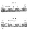
- the compliant pads 110 are typically formed and attached to the dielectric film 100 using a stencil mask 80 having top and bottom surfaces and further having a plurality of holes 90 extending therethrough.
- the bottom surface of the mask 80 is placed atop the first surface of the film 100 and curable liquid elastomer is wiped or screened across the first surface of the mask 80 so that the elastomer is deposited into each of the holes 90.
- the mask is then typically removed and the pads are cured or partially cured by heating or exposing them to ultra-violet light or a combination thereof, such as by exposing the elastomer to ultraviolet light to create a "skin" of cured elastomer and then curing or partially curing the elastomer by a heating step.
- the elastomer is typically heated to approximately 125o C for 40 minutes.
- the mask 80 may also be removed after the curing step. In this case, the elastomer will conform to the shape of the hole 90 in the mask as it begins to cure.
- the pads 110 in Figure 3A will be cylindrical in shape with substantially flat top surfaces. If the mask 80 is left atop the dielectric film 100 during the curing step, the pads may partially adhere to the mask 80 at an exposed top edge of each hole 90 on the first surface of the mask as the elastomer cures. This makes removal of the mask 80 while maintaining the integrity of the pads 110 difficult.
- This problem can be effectively dealt with by using an alternate stencil mask 85, shown in Figure 3B, where each hole in the mask has a smaller top edge circumference on the top surface of the mask 85 than on the bottom surface of the mask 85. The smaller circumference of each hole reduces the strength of the attachment of the compliant pads 110 to the mask 85.
- the liquid elastomer typically must be screened across the first surface of the mask in two directions to ensure the enclosure 95 is completely filled.
- the elastomer will then take on a rounded shape corresponding the shape of the enclosure 95 and will retain its shape after curing.
- the Dow 577 elastomer discussed above, also shrinks by approximately 5% during the curing step thereby facilitating the removal of the mask 85.
- Another solution to this problem would be to coat the mask 80 with a material that will resist the adherence of the elastomer as it cures.
- a semiconductor chip 120 is next abutted to the compliant pads 110.
- the chip 120 has a face surface bearing contacts 130 and a back surface.
- the face surface of the chip is aligned with the compliant pads so that the none of the pads 110 cover the contacts on the chip.
- the dielectric film 100 and the second support structure or chip 120 are squeezed together between a first platen 107 and a second platen 127.
- the platens are urged toward one another by a press (not shown).
- the first platen bears on the terminals 140 of the film 100, and forces these terminals into substantially coplanar alignment, whereas the second platen bears on the back surface of chip 120.
- the pads 110 are compressed.
- the pads 110 are tacky and adhere to the chip 120 when it is compressed thereagainst.
- the chip 120 would be heated to about 100° to 180° C and then compressed against the pads 110 so that the partially cured pads 110 fully cure due to the heat of the chip 120 and in so doing adhere to the face surface of the chip.
- the apex of each pad may be made tacky by providing an adhesive, a silicone gel, or a film of uncured silicone elastomer thereon so that the chip 120 adheres thereto.
- the chip surface may be coated with an adhesive in the regions remote from the contacts 130 so that the tips of the pads 110 engage such adhesive.
- the pads 110 While adherence of the pads 110 to the chip 120 helps maintain the alignment between the chip 120 and the film 100, it is not imperative that the pads 110 are adhered to the chip 120 so long as the chip can be held in place by compressing it against the pads 110.
- the heat and pressure applied during this step of the process permanently deform or "set" the pads to the heights and shapes achieved when the film and chip are squeezed between the platens. Once set in this manner, the pads tend to retain the film and chip in the same relative positions as achieved during the squeezing step, and thereby tend to retain the terminals 140 in coplanar alignment with one another.
- each contact 130 on the chip 120 is then attached to the terminals 140 on the film 100 through any suitable means.
- each contact 130 is electrically connected to one terminal 140 through a flexible lead 150 extending therebetween.
- the terminal 140 is comprised of a conductive blind via (a via extending from the second to the first surface of the film 100 and having a closed bottom surface substantially in a plane with the first surface of the dielectric film 100) and a solder ball (shown in dashed lines), which is typically attached after the package is complete.
- a low viscosity compliant filler 170 is then disposed between the chip 120 and the dielectric film 100 through the channels between the adjacent pads 110.
- An injection nozzle 160 is disposed adjacent an edge of the film 100.
- the filler 170 passes through the nozzle into the channels 117.
- the compliant filler 170 may be comprised of an elastomer, a gel or a compliant thixotropic material so long as the elastomer, gel or material retains its compliancy.
- a filler is Dow Corning elastomer Q1-4939.
- the filler 170 is comprised of a curable liquid elastomer having a viscosity adapted to facilitate flow of the liquid into the channels 117 between the adjacent pads 110.
- An evacuated environment can also be provided during the elastomer flow so that voids in the liquid elastomer caused by trapped air may be eliminated. Capillary action tends to pull the low viscosity liquid elastomer 170 into the channels 117 as the elastomer wets the pads, the chip and the film.
- the liquid elastomer 170 tends to remain between the chip and the substrate because of the surface tension forces. If necessary, however, the edges of the assembly may be closed by any suitable means to trap the liquid 170.
- the liquid elastomer also encapsulates leads 150.
- the liquid 170 is then cured, typically by heating the assembly while it is held between flat opposing surfaces, such as the platens 107, 127 used for the compression step. This results in a planar, compliant interface between the chip 120 and the dielectric film 100. The resulting assembly may then be freed to form an individual semiconductor chip package.
- the function of the compliant pads is to provide a uniformly supported, planar standoff between the chip and the dielectric film, while allowing the compliant filler to be injected between the adjacent pads 110 to create a compliant encapsulation layer having a controlled thickness. So long as there is uniformity of support, it does not matter whether the pads 110 are in direct registration with single or multiple terminals 140, as shown in Figures 4A and 4B, or whether the pads 110 are in random registration with respect to the terminals 140, as shown in Figure 4C. It also does not matter whether all of the pads in a common array are of the same general shape or dimension.
- FIG. 5A shows a top plan of a preferred embodiment of the first support structure and the compliant pads.
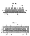
- Tape 200 is a continuous elongated strip of film with handling and locating features such as sprocket holes 210 adapted for engagement by tape-handling equipment of the type commonly employed in tape automated bonding or "TAB" processing in the semiconductor industry.
- Tape 200 includes a plurality of regions 201 spaced apart along its length, each such region constituting a support structure for one chip.
- Each region has pads 220 disposed in a grid on its first surface so that the pads define channels 203 therebetween, and has terminals 207 on its second surface, the terminals being connected to leads 225 extending across an aperture or "bond window" 215 in the tape, the bond window being in the form of a slot extending around a rectangular loop.
- the leads are adapted for bonding to the contacts of the chip.
- each lead may have a detachable section as disclosed in International Patent Publication WO 94/03036, the disclosure of which is hereby incorporated by reference herein.
- the terminals and leads can be arranged in a "fan out” pattern, wherein the terminals are disposed on that portion of the tape outside of the loop defined by the bond window; in a "fan in” pattern wherein the terminals are disposed on that portion of the tape encircled by the bond window; or both.
- a tape can be mass-produced, to include numerous regions.
- a series of chips can be bonded to the various regions of the tape by abutting each chip against the compliant pads of one region and compressing and bonding the chip and pads in the same manner as discussed above.
- Each pad 220 may be only partially cured, or else may have a tacky layer 230 (Fig. 5B) of adhesive, silicone gel or uncured silicone elastomer on its apex, so that the pads will adhere to the chip.
- the chip may have such a tacky layer on its first surface in areas remote from the contacts.
- the tape is juxtaposed with each chip so that one region of the tape overlies the chip, and the contacts of each chip are brought into coarse alignment with the leads of the associated region of the tape, using conventional machine-vision alignment techniques. This alignment is maintained during the compressing and pad bonding steps. After the pads have been bonded to the surfaces of the chip, the bonded pads maintain the alignment of the leads and contacts.
- the terminals of each region are electrically connected to the contacts of the associated chip, as by advancing a bonding tool into the bond window to engage each lead and connect it to the aligned contact of the chip.
- the bonding tool captures the bond region of the lead and brings it into more precise alignment with the chip contact.
- the compliant filler is introduced into the channels 203 between the pads, in substantially the same way as described above.
- the film 200 and the chip are compressed while the liquid material is introduced.
- These operations may be performed at separate stations of a processing line.
- the chip can be transported to the next station of the processing line by moving the tape using the sprocket holes 210.
- Each region of the tape can be severed from the remainder of the tape after all of the process steps have been completed to provide an individual chip and film assembly.
- each region can be severed before the final process step, and a portion of the process can be completed after severance.
- a plurality of individual regions of the tape may remain connected to one another,
- each of these leads 225 will be detached within or near an edge of the bonding window 215 when such lead is connected to a respective chip contact pad. If the leads and the terminals are arranged in a fan-out pattern, this action detaches the tape center portion 205, generally centered within the loop defined as the bonding window 215 from the outer portions of the tape. However, the compliant pads 220 disposed on the tape center portion 205 provides support for the leads 225 during the bonding phase. Conversely, in a fan-in arrangement, the exterior portion of each region may optionally be removed after connecting the leads.
- a plurality of individual regions 201 of the tape remain together and are not severed from one another during the process.
- a short length of tape thus retains a plurality of chips side-by-side, as a multi-chip module.
- the back surfaces of these chips or modules may be mated to heat spreader/sinks 270 before or after the step of cutting the short length of tape bearing the chips free from the remainder of the tape.
- a thermally conductive die attach material may be used between the chips 240 and the heat spreader 270 to aid in the transfer of heat from the chips. Such die attach materials are widely used in the semiconductor industry.
- a plurality of individual regions are formed side-by-side in a two-dimensional array on a unitary film in the shape of a panel.
- Plural chips are attached to these regions in the same manner as discussed above, so as to form a multichip assembly.
- the steps of abutting and compressing the pads and injecting the liquid compliant filler can be performed simultaneously for all of the chips, using platens large enough to accommodate the entire array, or seriatim so that each chip is processed separately.
- Figure 6 shows a side view of a compliant interface, as described in reference to Figures 1 and 2, being formed between a second support structure or semiconductor wafer 350 having contacts (not shown) on a first surface and a first support structure or film 300.
- the wafer 350 includes an integral plurality of individual chips, each defining a portion of the first surface, and each including a plurality of contacts thereon.
- the film 300 has terminals 305 on its second surface, with leads (not shown) connected to the terminals 305.
- the terminals 305 and leads are disposed in a plurality of regions, each corresponding to one chip.
- Each region of the film may include a bond window (not shown), as discussed above.
- compliant pads 320 defining channels 325 therebetween are formed on the first surface of the film.
- each pad 320 may be only partially cured, or may have a curable tacky material on its apex.
- the film 300 is stretched taut and bonded to a rigid ring structure 310.
- the film 300 is then aligned with the wafer so that each region of the film is aligned with one chip of the wafer, and so that the leads are aligned with the contacts.
- the wafer is then abutted against the compliant pads 320.
- a platen 360 is applied on the back surface of the wafer 350.
- Another platen 370 is applied on the second surface of the film so as to engage the terminals 305.
- the platens are forced toward one another, thereby compressing pads 320 and bringing the contacts 303 into substantially coplanar alignment with one another. While the contacts and pads are held in this position, the pads may be fully cured or set by heating the platen 360/wafer 350, thereby securing the film in position on the wafer. Alternately, a tacky adhesive may be applied to the first surface of the wafer around the contacts thereon to ensure the adherence of the pads 320 to the wafer 350. After this operation, the leads are bonded to the wafer contacts, followed by injection of the liquid curable elastomer 340 into the channels 325. While the contacts are again held in position by the platens, the liquid elastomer is cured to form a complete assembly encompassing the entire wafer and all regions of the film.
- Figure 7 shows a further embodiment having an array of compliant pads 410 held in place using a holding element 400.
- the pads 410 are then fixably placed atop either the contact bearing surface of a semiconductor chip (second support structure) or a flexible dielectric film (first support structure) typically by placing a tacky adhesive onto one of those surfaces.
- the holding element 400 is then removed.
- the holding element 400 is made of a material which will break apart or peel off the pads easily so that the adherence of the pads 410 to either the wafer or the film is not comprised.
- the pads 110, as shown in Figure 1, are not typically screened across and cured to the contact bearing surface of the chip for fear that the contacts will be contaminated by stray uncured elastomer.
- the pads are being attached after they have been either fully cured or partially cured to the point that they may retain their individual structural integrity.
- the pads 410 may be accurately placed and typically adhered on the chip's surface without any substantial fear that the chip's contacts will be contaminated.
- the pads are then compressed between the chip and the supporting substrate using platens and liquid elastomer is next injected into the channels between the adjacent pads and cured, as described more fully in relation to the above embodiments.
- FIG. 8 shows a side view of an alternate embodiment in which the pads 510 are compressed between a second support structure which includes a heat spreader 520 having an indentation on its first side and a first support structure 500, which includes a flexible dielectric film.
- a chip 530 is disposed within the indentation of the heat spreader 520 so that the front or contact-bearing surface 580 of the chip faces outwardly at the opening of the indentation, and thus faces outwardly from the first surface 570 of the heat spreader.
- Dielectric film 500 has a bond window 550, terminals 590 on one surface and leads 595 connected to the terminals 590.
- the dielectric film 500 and the heat spreader 520 are aligned so that the outer portions of the dielectric film overly the first surface 570, and so that the bond window 550 is aligned with the contacts on the chip.
- the leads 595 are bonded to the contacts of the chip.
- the bond window is closed by a sheet 540 of a further dielectric material such as a solder mask material which adheres to film 500 and thus forms a continuation of the film 500.
- the pads 510 are compressed against first surface 570 by engaging the heat spreader 520 and the film 500 between a pair of platens (not shown) so that one such platen bears on the rear surface of the heat spreader, opposite from surface 570 and so that the other platen bears on terminals 590.
- This compression brings the terminals into coplanar alignment.
- the liquid compliant filler 560 is injected into the channels between the pads and cured while the platens hold the system in compression.
- the pads are not provided at the interface between sheet 540 and the chip 530.
- a compliant filler material 560 may be injected between the adjacent pads 510 creating a planar, compliant interface while simultaneously encapsulating the chip 530.
- the invention can be employed for mounting semiconductor chips.
Abstract
Description
- The present invention relates, generally to providing a compliant interface for a semiconductor chip, and more particularly relates to a method and apparatus for providing a compliant interface to accommodate for differences in the thermal coefficient of expansion mismatch between a semiconductor chip and a support structure, such as a printed wiring board.
- In attempting to use the area on printed wiring boards more efficiently, semiconductor chip manufacturers have recently been switching from larger, more cumbersome interconnection conventions, such as pin grid arrays ("PGAs") and the perimeter leaded quad flat packs ("QFPs"), to smaller conventions, such as ball grid arrays ("BGAs"). Using BGA technology, semiconductor chips are typically interconnected to their supporting substrates using solder connections, such as with "flip-chip" technology. However, when solder alone is used to interconnect the chip contacts to the substrate, the columns of solder are generally designed to be short to maintain the solder's structural integrity. This results in minimal elastic solder connection properties which further results in increased susceptibility to solder cracking due to the mechanical stress of the differential thermal coefficient of expansion ("TCE") of the chip relative to the supporting substrate thereby reducing the reliability of the solder connection. In other words, when the chip heats up during use, both the chip and the substrate expand; and when the heat is removed, both the chip and the substrate contract. The problem that arises is that the chip and the substrate expand and contract at different rates and at different times, thereby stressing the interconnections between them. As the features of semiconductor chips continue to be reduced in size, the number of chips packed into a given area will be greater and the heat dissipated by the each of these chips will have a greater effect on the thermal mismatch problem.
This further increases the need for a highly compliant interconnection scheme for the chips. - The solder cracking problem is exacerbated when more than one semiconductor chip is mounted in a package, such as in a multichip module. Multi-chip modules continue to grow in popularity; however, as more chips are packaged together, more heat will be dissipated by each package which, in turn, means the interconnections between a package and its supporting substrate will encounter greater mechanical stress due to thermal cycling. Further, as more chips are integrated into multichip modules, each package requires additional interconnections thereby increasing the overall rigidity of the connection between the module and its supporting substrate.
- An interconnection solution put forth in U.S. Patent No. 4,642,889, entitled "Compliant Interconnection and Method Therefor" issued to Grabbe seeks to alleviate the aforementioned solder cracking problem by embedding wires within each solder column to reinforce the solder thereby allowing higher solder pedestals and more elasticity. Another solution includes spirally wrapping wire around the outside of the solder. A further solution put forth includes providing a combination of solder and high lead solder, as found in U.S. Patent No. 5,316,788, entitled "Applying Solder to High Density Substrates" issued to Dibble et al.
- Still other prior art solutions make use of a underfill material disposed between the chip and the supporting substrate in an attempt to reduce the stress caused by TCE mismatch. Without the underfill material, this stress is typically concentrated at the weakest part of the solder balls. The underfill material allows this stress to be more uniformly spread out over the entire surface of the solder balls. Examples of the use of underfill materials may be found in U.S. Patent Nos. 5,194,930, 5,203,076 and 5,249,101. All of these prior art solutions are aimed at reducing the shear stress endured by the interconnections caused by thermal cycling. However, each of these solutions also encounters significant problems such as insufficient compliancy and process cost.
- Several inventions, commonly assigned to the assignee of the present invention, deal effectively, but specifically differently, with the thermal cycling problem. For example, U.S. Patent No. 5,148,266 discloses improvements in semiconductor chip assemblies and methods of making the same. As set forth in the '266 patent, a semiconductor chip can be connected to a substrate using a sheet-like, and preferably flexible, interposer. The interposer overlies the top, contact-bearing surface of the chip. A first surface of the interposer faces towards the chip whereas a second surface faces away from the chip. Electrical terminals are provided on the second surface of the interposer, and the interposer is provided with apertures extending through it. Flexible leads extend through these apertures between contacts on the chip and the terminals on the second surface of the interposer. The terminals can be bonded to a substrate. Because the terminals are movable relative to the contacts on the chip, the arrangements described in the '266 patent provide excellent resistance to differential expansion of the chip relative to the substrate caused by thermal cycling. The interposer disclosed in the '266 patent may also include a compliant layer disposed between the terminals and the chip.
- Copending, commonly assigned United States Patent Application No. 08/123,882, filed September 20, 1993, discloses a method for creating an interface between a chip and chip carrier including spacing the chip a given distance above the chip carrier, and introducing a liquid in the gap between the chip and carrier. Preferably, the liquid is an elastomer which is cured into a resilient layer after its introduction into the gap. In another preferred embodiment, the terminals on a chip carrier are planarized or otherwise vertically positioned by deforming the terminals into set vertical locations with a plate, and a liquid is then cured between the chip carrier and chip.
- Document "Area Array Chip Carrier : SMT Package for Known Good Die", ISHM '93 Producings, P. 318-333, discloses a compliant filler interface, wherein an elastomeric pad occupies the space between chip and carrier.
- Despite the positive results of the aforementioned commonly owned inventions, still further improvements would be desirable.
- The present invention as defined in claims 1 and 33 provides a method and apparatus for providing a compliant interface for semiconductor chips to accommodate for the typically large thermal expansion mismatch between a chip and its support structure.
- More specifically, one aspect of the present invention provides a method of fabricating a compliant interface for a semiconductor chip, typically comprised of a compliant encapsulation layer having a controlled thickness. A first support structure, such as a flexible, substantially inextensible dielectric film, having a surface is provided. A plurality of compliant pads are attached to the first surface of the first support structure, any two adjacent compliant pads defining a channel therebetween. Attaching the compliant pads to the first support structure may be accomplished a number of different ways. In one embodiment, a stencil mask having a plurality of holes extending therethrough is placed on top of the first surface of the support structure. The holes in the mask are then filled with a curable liquid elastomer. Desirably, liquid elastomer has a thick enough consistency so that the mask may then be removed before curing the elastomer. After the mask has been removed, the elastomer is at least partially cured, such as by heating or exposing to ultra-violet light. The filling step may be accomplished by screening the liquid elastomer across an exposed surface of the mask such that the elastomer is deposited into the holes of the mask. Other methods are also suitable, such as dispensing the elastomer into each of the holes individually. Thus, there is provided an assembly which includes an array of compliant pads further having channels between substantially all of the adjacent pads.
- At this stage of the process, the vertical height of the pads need not be extremely uniform.
- In a further stage, the assembly including the array of pads is used with a second support structure. In one embodiment, the second support structure is a semiconductor chip having a plurality of contacts on a first surface. The first surface of the chip is abutted against the array of compliant pads and the contacts are electrically connected to a corresponding plurality of terminals on a second side of the support structure. Typically, the first surface of the chip is pressed against the pads to compress them, thus ensuring the chip is uniformly supported across its first surface and further ensuring the planarity of the first support structure, or flexible dielectric film, with respect to the first surface of the chip. Where the dielectric film has terminals thereon, the terminals desirably are held coplanar with one another during this step. For example, the dielectric film and the chip may be held between a pair of opposed platens, so that the terminals bear on one platen and are brought into a substantially coplanar condition. A compliant filler, such as a curable liquid elastomer, is then injected into the channels between the chip and the support structure and around the compliant pads while the chip and support structure are held in place. The elastomer may then be cured to form a substantially uniform, planar, compliant layer between the chip and the support structure.
- In a further embodiment, the second support structure includes a plurality of chips. The array of compliant pads is large enough to overly several chips simultaneously. This method may be used to form a compliant interface for multiple chips which then may either be cut into individual chips or may be used as a multi-chip module. The above method may also be used to form a compliant interface for a semiconductor wafer before the individual chips are separated. After the compliant interface is formed, the wafer may be cut into individual chips or into multi-chip modules.
- A further embodiment provides for an array of compliant pads held in place using a holding element. The pads are then fixably placed to either a surface of the chip or the supporting substrate. The holding element is then removed and the pads are compressed between the chip and the supporting substrate. Liquid elastomer is injected into the channels between the adjacent pads, as described in the above embodiments.
- The pads or the pad/injected elastomer combination provide a compliant, planar interface which effectively accommodates for the thermal coefficient of expansion mismatch between the chip and a supporting substrate thereby alleviating much of the stress on the connections therebetween. Further, the combination provides an effective encapsulation barrier against moisture and contaminants.
- The foregoing and other objects and advantages of the present invention will be better understood from the following Detailed Description of a Preferred Embodiment, taken together with the attached Figures.
-
- Figure 1 shows a side view of one embodiment of a compliant semiconductor chip interface having a plurality of compliant pads, according to the present invention.
- Figure 2 shows a side view of the embodiment shown in Figure 1, wherein the channels between the compliant pads are filled with a curable liquid, according to the present invention.
- Figures 3A and 3B show a side view of the mask and elastomer used to form the compliant pads, according to further embodiments of the invention.
- Figures 4A-C show a top plan view of several different pad shapes and registrations in relation to the terminal's positions, according to further embodiments of the invention.
- Figures 5A and 5B show a perspective and a side view of the support structure and compliant pads, according to a further embodiment of the present invention.
- Figure 5C shows a side view of the embodiment shown in Figures 5A and 5B, wherein multiple encapsulated chips have been abutted against the compliant pads.
- Figure 6 shows a side view of a compliant interface being formed between a wafer and the support structure, according to a further embodiment of the present invention.
- Figure 7 shows a side view of a plurality of compliant pads disposed within holes in a holding element, according to a further embodiment of the present invention.
- Figure 8 shows a side view of a further embodiment of the invention having a compliant interface between a heat spreader and a support structure.
-
- Figures 1 and 2 show a side view of a chip size package embodiment, according to the present invention. A
support structure 100 is provided having a first and a second surface. Thesupport structure 100 may be substantially rigid, semi-rigid or flexible. However typically, thesupport structure 100 is comprised of a flexible, but substantially inextensible, dielectric film, preferably formed from a polymeric material, such as Kapton™ "E" available from DuPont Chemical Corp., of an approximate thickness between 25 microns and 75 microns. Further, thedielectric film 100 typically hasconductive terminals 140 on its second surface. - A plurality of dielectric
compliant pads 110 are attached to the first surface of thefilm 100. Thecompliant pads 110 are typically made of an curable liquid elastomer material, such as the Dow Corning silicone elastomer 577, known as "Sylgard™", with about 5-10% of fumed silica in order to obtain a stiff, thixotropic consistency. The height of thecompliant pads 110 is nominally uniform, as defined by the measurement from the base of the pads, at the first surface of the film, to the apexes of the pads.
However, exact uniformity in height is not critical, as discussed below. The ratio of width to height of eachpad 110 is desirably about two to one (2:1) or greater in order to maintain good pad structural integrity. Each pad desirably has width or diameter, measured at its juncture with first surface of thefilm 100, between about 300 µm to 2000 µm. The pads are arranged in a grid pattern with center-to-center distance or "pitch" greater than the minimum width of each pad and preferably greater than the maximum width of each pad. Thus, each pair of mutually adjacent pads defines achannel 117 between them, and all of the channels are interconnected with one another to define a substantially continuous grid ofchannels 117. The pad pitch and hence the width of thechannels 117 must be large enough to allow acompliant filler material 170 to be injected into thechannels 117, as described in greater detail below. - As shown in Figure 3A and 3B, the
compliant pads 110 are typically formed and attached to thedielectric film 100 using astencil mask 80 having top and bottom surfaces and further having a plurality of holes 90 extending therethrough. In a preferred embodiment, the bottom surface of themask 80 is placed atop the first surface of thefilm 100 and curable liquid elastomer is wiped or screened across the first surface of themask 80 so that the elastomer is deposited into each of the holes 90. If the elastomer is viscous or thixotropic enough, the mask is then typically removed and the pads are cured or partially cured by heating or exposing them to ultra-violet light or a combination thereof, such as by exposing the elastomer to ultraviolet light to create a "skin" of cured elastomer and then curing or partially curing the elastomer by a heating step. In the case of Dow 577 elastomer, the elastomer is typically heated to approximately 125º C for 40 minutes. Themask 80 may also be removed after the curing step. In this case, the elastomer will conform to the shape of the hole 90 in the mask as it begins to cure. Thus, thepads 110 in Figure 3A will be cylindrical in shape with substantially flat top surfaces. If themask 80 is left atop thedielectric film 100 during the curing step, the pads may partially adhere to themask 80 at an exposed top edge of each hole 90 on the first surface of the mask as the elastomer cures. This makes removal of themask 80 while maintaining the integrity of thepads 110 difficult. This problem can be effectively dealt with by using analternate stencil mask 85, shown in Figure 3B, where each hole in the mask has a smaller top edge circumference on the top surface of themask 85 than on the bottom surface of themask 85. The smaller circumference of each hole reduces the strength of the attachment of thecompliant pads 110 to themask 85. However, because of the shape ofenclosure 95 of the embodiment shown in Figure 3B, the liquid elastomer typically must be screened across the first surface of the mask in two directions to ensure theenclosure 95 is completely filled. The elastomer will then take on a rounded shape corresponding the shape of theenclosure 95 and will retain its shape after curing. The Dow 577 elastomer, discussed above, also shrinks by approximately 5% during the curing step thereby facilitating the removal of themask 85. Another solution to this problem would be to coat themask 80 with a material that will resist the adherence of the elastomer as it cures. - Returning to Figure 1, a
semiconductor chip 120 is next abutted to thecompliant pads 110. Thechip 120 has a facesurface bearing contacts 130 and a back surface. The face surface of the chip is aligned with the compliant pads so that the none of thepads 110 cover the contacts on the chip. In the next step of the operation, thedielectric film 100 and the second support structure orchip 120 are squeezed together between afirst platen 107 and asecond platen 127. The platens are urged toward one another by a press (not shown). The first platen bears on theterminals 140 of thefilm 100, and forces these terminals into substantially coplanar alignment, whereas the second platen bears on the back surface ofchip 120. During this process, thepads 110 are compressed. The extent of such compression varies from pad to pad, depending upon the original height of each pad, the heights of thevarious terminals 140 and other tolerances. Because the pads can accommodate variations in this manner, the heights of the pads prior to compression need not be precisely uniform. Some particularly short pads, such aspad 115, may not contact the chip surface even after compression. This situation is acceptable provided that the remaining pads substantially support theterminals 140 against the first platen. - Where the
pads 110 are only partially cured during the pad forming process, described above, they are tacky and adhere to thechip 120 when it is compressed thereagainst. In a preferred embodiment, thechip 120 would be heated to about 100° to 180° C and then compressed against thepads 110 so that the partially curedpads 110 fully cure due to the heat of thechip 120 and in so doing adhere to the face surface of the chip. Alternately, the apex of each pad may be made tacky by providing an adhesive, a silicone gel, or a film of uncured silicone elastomer thereon so that thechip 120 adheres thereto. Similarly, the chip surface may be coated with an adhesive in the regions remote from thecontacts 130 so that the tips of thepads 110 engage such adhesive. While adherence of thepads 110 to thechip 120 helps maintain the alignment between thechip 120 and thefilm 100, it is not imperative that thepads 110 are adhered to thechip 120 so long as the chip can be held in place by compressing it against thepads 110. The heat and pressure applied during this step of the process permanently deform or "set" the pads to the heights and shapes achieved when the film and chip are squeezed between the platens. Once set in this manner, the pads tend to retain the film and chip in the same relative positions as achieved during the squeezing step, and thereby tend to retain theterminals 140 in coplanar alignment with one another. - The
contacts 130 on thechip 120 are then attached to theterminals 140 on thefilm 100 through any suitable means. In this embodiment, eachcontact 130 is electrically connected to oneterminal 140 through aflexible lead 150 extending therebetween. The terminal 140 is comprised of a conductive blind via (a via extending from the second to the first surface of thefilm 100 and having a closed bottom surface substantially in a plane with the first surface of the dielectric film 100) and a solder ball (shown in dashed lines), which is typically attached after the package is complete. - As shown in Figure 2, a low viscosity
compliant filler 170 is then disposed between thechip 120 and thedielectric film 100 through the channels between theadjacent pads 110. Aninjection nozzle 160 is disposed adjacent an edge of thefilm 100. Thefiller 170 passes through the nozzle into thechannels 117. Thecompliant filler 170 may be comprised of an elastomer, a gel or a compliant thixotropic material so long as the elastomer, gel or material retains its compliancy. One example of such a filler is Dow Corning elastomer Q1-4939. In a preferred embodiment, thefiller 170 is comprised of a curable liquid elastomer having a viscosity adapted to facilitate flow of the liquid into thechannels 117 between theadjacent pads 110. An evacuated environment can also be provided during the elastomer flow so that voids in the liquid elastomer caused by trapped air may be eliminated. Capillary action tends to pull the lowviscosity liquid elastomer 170 into thechannels 117 as the elastomer wets the pads, the chip and the film. Theliquid elastomer 170 tends to remain between the chip and the substrate because of the surface tension forces. If necessary, however, the edges of the assembly may be closed by any suitable means to trap the liquid 170. During this process, the liquid elastomer also encapsulates leads 150. The liquid 170 is then cured, typically by heating the assembly while it is held between flat opposing surfaces, such as theplatens chip 120 and thedielectric film 100. The resulting assembly may then be freed to form an individual semiconductor chip package. - It is important to understand that the function of the compliant pads is to provide a uniformly supported, planar standoff between the chip and the dielectric film, while allowing the compliant filler to be injected between the
adjacent pads 110 to create a compliant encapsulation layer having a controlled thickness. So long as there is uniformity of support, it does not matter whether thepads 110 are in direct registration with single ormultiple terminals 140, as shown in Figures 4A and 4B, or whether thepads 110 are in random registration with respect to theterminals 140, as shown in Figure 4C. It also does not matter whether all of the pads in a common array are of the same general shape or dimension. - Figure 5A shows a top plan of a preferred embodiment of the first support structure and the compliant pads.
Tape 200 is a continuous elongated strip of film with handling and locating features such as sprocket holes 210 adapted for engagement by tape-handling equipment of the type commonly employed in tape automated bonding or "TAB" processing in the semiconductor industry.Tape 200 includes a plurality ofregions 201 spaced apart along its length, each such region constituting a support structure for one chip. Each region haspads 220 disposed in a grid on its first surface so that the pads definechannels 203 therebetween, and hasterminals 207 on its second surface, the terminals being connected toleads 225 extending across an aperture or "bond window" 215 in the tape, the bond window being in the form of a slot extending around a rectangular loop. The leads are adapted for bonding to the contacts of the chip. For example, each lead may have a detachable section as disclosed in International Patent Publication WO 94/03036, the disclosure of which is hereby incorporated by reference herein. The terminals and leads can be arranged in a "fan out" pattern, wherein the terminals are disposed on that portion of the tape outside of the loop defined by the bond window; in a "fan in" pattern wherein the terminals are disposed on that portion of the tape encircled by the bond window; or both. Such a tape can be mass-produced, to include numerous regions. - In use, a series of chips can be bonded to the various regions of the tape by abutting each chip against the compliant pads of one region and compressing and bonding the chip and pads in the same manner as discussed above. Each
pad 220 may be only partially cured, or else may have a tacky layer 230 (Fig. 5B) of adhesive, silicone gel or uncured silicone elastomer on its apex, so that the pads will adhere to the chip. Alternatively or additionally, the chip may have such a tacky layer on its first surface in areas remote from the contacts. During the abutting step, the tape is juxtaposed with each chip so that one region of the tape overlies the chip, and the contacts of each chip are brought into coarse alignment with the leads of the associated region of the tape, using conventional machine-vision alignment techniques. This alignment is maintained during the compressing and pad bonding steps. After the pads have been bonded to the surfaces of the chip, the bonded pads maintain the alignment of the leads and contacts. The terminals of each region are electrically connected to the contacts of the associated chip, as by advancing a bonding tool into the bond window to engage each lead and connect it to the aligned contact of the chip. - Preferably, the bonding tool captures the bond region of the lead and brings it into more precise alignment with the chip contact. After bonding the leads, the compliant filler is introduced into the
channels 203 between the pads, in substantially the same way as described above. Typically, thefilm 200 and the chip are compressed while the liquid material is introduced. These operations may be performed at separate stations of a processing line. At any time after the pads of a region have been bonded to a chip, the chip can be transported to the next station of the processing line by moving the tape using the sprocket holes 210. Each region of the tape can be severed from the remainder of the tape after all of the process steps have been completed to provide an individual chip and film assembly. Alternatively, each region can be severed before the final process step, and a portion of the process can be completed after severance. In a further embodiment of the invention, a plurality of individual regions of the tape may remain connected to one another, - Typically, each of these
leads 225 will be detached within or near an edge of thebonding window 215 when such lead is connected to a respective chip contact pad. If the leads and the terminals are arranged in a fan-out pattern, this action detaches thetape center portion 205, generally centered within the loop defined as thebonding window 215 from the outer portions of the tape. However, thecompliant pads 220 disposed on thetape center portion 205 provides support for theleads 225 during the bonding phase. Conversely, in a fan-in arrangement, the exterior portion of each region may optionally be removed after connecting the leads. - In the alternative embodiment shown in Figure 5C, a plurality of
individual regions 201 of the tape remain together and are not severed from one another during the process. A short length of tape thus retains a plurality of chips side-by-side, as a multi-chip module. Thus, as illustrated in Fig. 5C, the back surfaces of these chips or modules may be mated to heat spreader/sinks 270 before or after the step of cutting the short length of tape bearing the chips free from the remainder of the tape. Further, a thermally conductive die attach material may be used between thechips 240 and theheat spreader 270 to aid in the transfer of heat from the chips. Such die attach materials are widely used in the semiconductor industry. - In a further alternative arrangement, a plurality of individual regions, each adapted to form a support structure for an individual chip, are formed side-by-side in a two-dimensional array on a unitary film in the shape of a panel. Plural chips are attached to these regions in the same manner as discussed above, so as to form a multichip assembly. In either arrangement where plural chips are employed, the steps of abutting and compressing the pads and injecting the liquid compliant filler can be performed simultaneously for all of the chips, using platens large enough to accommodate the entire array, or seriatim so that each chip is processed separately.
- Figure 6 shows a side view of a compliant interface, as described in reference to Figures 1 and 2, being formed between a second support structure or
semiconductor wafer 350 having contacts (not shown) on a first surface and a first support structure orfilm 300. - The
wafer 350 includes an integral plurality of individual chips, each defining a portion of the first surface, and each including a plurality of contacts thereon. Thefilm 300 hasterminals 305 on its second surface, with leads (not shown) connected to theterminals 305. Theterminals 305 and leads are disposed in a plurality of regions, each corresponding to one chip. Each region of the film may include a bond window (not shown), as discussed above. - Before engagement with the
wafer 350,compliant pads 320 definingchannels 325 therebetween are formed on the first surface of the film. Here again, eachpad 320 may be only partially cured, or may have a curable tacky material on its apex. Thefilm 300 is stretched taut and bonded to arigid ring structure 310. Thefilm 300 is then aligned with the wafer so that each region of the film is aligned with one chip of the wafer, and so that the leads are aligned with the contacts. The wafer is then abutted against thecompliant pads 320. Aplaten 360 is applied on the back surface of thewafer 350. Anotherplaten 370 is applied on the second surface of the film so as to engage theterminals 305. In the same manner as described above, the platens are forced toward one another, thereby compressingpads 320 and bringing the contacts 303 into substantially coplanar alignment with one another. While the contacts and pads are held in this position, the pads may be fully cured or set by heating theplaten 360/wafer 350, thereby securing the film in position on the wafer. Alternately, a tacky adhesive may be applied to the first surface of the wafer around the contacts thereon to ensure the adherence of thepads 320 to thewafer 350. After this operation, the leads are bonded to the wafer contacts, followed by injection of the liquidcurable elastomer 340 into thechannels 325. While the contacts are again held in position by the platens, the liquid elastomer is cured to form a complete assembly encompassing the entire wafer and all regions of the film. - Individual, fully encapsulated parts may then be cut from the wafer. These separated parts will have a compliant interface to accommodate for the thermal coefficient of expansion mismatch between the parts and their eventual supporting substrates, such as printed wiring boards. Further, the encapsulant protects the individual parts from moisture and contaminants.
- Figure 7 shows a further embodiment having an array of
compliant pads 410 held in place using a holdingelement 400. Thepads 410 are then fixably placed atop either the contact bearing surface of a semiconductor chip (second support structure) or a flexible dielectric film (first support structure) typically by placing a tacky adhesive onto one of those surfaces. The holdingelement 400 is then removed. Desirably, the holdingelement 400 is made of a material which will break apart or peel off the pads easily so that the adherence of thepads 410 to either the wafer or the film is not comprised. Thepads 110, as shown in Figure 1, are not typically screened across and cured to the contact bearing surface of the chip for fear that the contacts will be contaminated by stray uncured elastomer. In the embodiment shown in Figure 7, however, the pads are being attached after they have been either fully cured or partially cured to the point that they may retain their individual structural integrity. Thus, thepads 410 may be accurately placed and typically adhered on the chip's surface without any substantial fear that the chip's contacts will be contaminated. The pads are then compressed between the chip and the supporting substrate using platens and liquid elastomer is next injected into the channels between the adjacent pads and cured, as described more fully in relation to the above embodiments. - The embodiment shown in Figure 8 shows a side view of an alternate embodiment in which the
pads 510 are compressed between a second support structure which includes aheat spreader 520 having an indentation on its first side and afirst support structure 500, which includes a flexible dielectric film. Achip 530 is disposed within the indentation of theheat spreader 520 so that the front or contact-bearingsurface 580 of the chip faces outwardly at the opening of the indentation, and thus faces outwardly from thefirst surface 570 of the heat spreader.Dielectric film 500 has abond window 550,terminals 590 on one surface and leads 595 connected to theterminals 590. Afterpads 510 are provided on thedielectric film 570 or the heat spreader by any of the techniques discussed above, thedielectric film 500 and theheat spreader 520 are aligned so that the outer portions of the dielectric film overly thefirst surface 570, and so that thebond window 550 is aligned with the contacts on the chip. The leads 595 are bonded to the contacts of the chip. After bonding the leads, the bond window is closed by asheet 540 of a further dielectric material such as a solder mask material which adheres to film 500 and thus forms a continuation of thefilm 500. Typically before bonding the leads, thepads 510 are compressed againstfirst surface 570 by engaging theheat spreader 520 and thefilm 500 between a pair of platens (not shown) so that one such platen bears on the rear surface of the heat spreader, opposite fromsurface 570 and so that the other platen bears onterminals 590. This compression brings the terminals into coplanar alignment. As described above, the liquidcompliant filler 560 is injected into the channels between the pads and cured while the platens hold the system in compression. In this embodiment, the pads are not provided at the interface betweensheet 540 and thechip 530. If asolder mask 540, or other suitable containing means, is placed over thebonding window 550, acompliant filler material 560 may be injected between theadjacent pads 510 creating a planar, compliant interface while simultaneously encapsulating thechip 530. - Having fully described several embodiments of the present invention, it will be apparent to those of ordinary skill in the art that numerous alternatives and equivalents exist which do not depart from the invention set forth above. It is therefore to be understood that the present invention is not to be limited by the foregoing description, but only by the appended claims.
- The invention can be employed for mounting semiconductor chips.
Claims (40)
- A method of fabricating a compliant interface for a semiconductor chip, comprising the steps of:providing a first support structure (100) having a first surface and a plurality of compliant dielectric pads on the first surface of the first support structure;abutting a first surface of a second support structure (120) against the compliant pads; characterized by the step ofdisposing a first curable liquid (170) in the channels between the plurality of compliant pads after the abutting step for forming a compliant filler constituted by dielectric material.
- The method as claimed in claim 1, wherein the first liquid is a curable elastomer or a curable gel encapsulant.
- The method as claimed in claim 1, further comprising the step of providing an evacuated environment prior to the disposing step.
- The method as claimed in claim 1 or 2, further characterized by the step of at least partially curing the first liquid after the first liquid has been introduced between the channels whereby a compliant layer is formed between the support structures.
- The method as claimed in claim 4, further characterized by the step of compressing the compliant pads (110) between the first and second support structures (100, 120) prior to the disposing step.
- The method as claimed in claim 5, wherein the compressing step includes the step of engaging the first and second support structure between a pair of opposed platens (107, 127) and urging the platens together.
- The method as claimed in claim 6, further characterized in that the first support structure has a plurality of terminals (140) on a second surface remote from the second support structure and one of the platens (107) bears on the terminals (140) so as to bring the terminals into substantially coplanar alignment with one another before the disposing step.
- The method as claimed in claim 7, wherein the compressing step includes the step of setting the compliant pads so that the pads tend to retain the terminals in said substantially coplanar alignment.
- The method as claimed in claim 8, further characterized in that the first support structure is a flexible dielectric sheet.
- The method as claimed in claim 1, further characterized in that the step of providing said first support structure includes the steps of:providing a mask (80) having a plurality of holes therethrough atop the first surface of the support structure (100) ;filling the holes in the mask with a second curable liquid;removing the mask; andat least partially curing the second liquid, whereby the compliant pads (110) are produced.
- The method as claimed in claim 10, wherein the step of curing the second liquid includes the step of heating the second liquid to between 100° to 180° C.
- The method as claimed in claim 10, wherein the step of curing the second liquid includes the step of exposing the second liquid to ultraviolet light.
- The method as claimed in claim 10, wherein the step of curing the second liquid includes the steps of at least partially curing the second liquid using a combination of ultraviolet light and heat.
- The method as claimed in claim 10, further characterized in that the filling step includes applying the second liquid across an exposed surface of the mask so that the second liquid fills the holes in the mask, and in that the holes (95) in the mask (85) have a smaller diameter at an exposed surface and a larger diameter at a surface adjacent the first surface of the dielectric sheet.
- The method as claimed in claim 9, further characterized in that the second support structure (120) is a semiconductor chip having a plurality of contacts (130) on the first surface thereof.
- The method as claimed in claim 15, further comprising the step of electrically connecting each contact (130) to one terminal (140) before the disposing step.
- The method as claimed in claim 16, further characterized in that the abutting step further includes aligning the chip so that no compliant pad covers a contact.
- The method as claimed in claim 17, further characterized by the step of heating the chip prior to compressing it against the compliant pads causing any partially cured pad to more fully cure and adhere to the chip.
- The method as claimed in claim 9, further characterized in that the second support structure includes a heat spreader (520) having an indentation on a first side, the method further comprising disposing a semiconductor chip (530) having contacts on a first surface within the indentation such that the contacts face outwardly toward the first surface of the first support structure (540).
- The method as claimed in claim 19, further characterized by the step of heating the heat spreader prior to compressing it against the compliant pads causing any partially cured pad to more fully cure and adhere to the heat spreader.
- The method as claimed in claim 19, further comprising the step of electrically connecting each contact to one terminal (540) prior to the disposing step.
- The method as claimed in claim 9, further characterized by the step of adhering a second surface of the second support structure to a contact bearing surface of a semiconductor chip having contacts thereon.
- The method as claimed in claim 22, further characterized in that the second support structure is a flexible dielectric sheet.
- The method as claimed in claim 1, wherein the step of providing further includes the steps of:providing a holding element (400) having a plurality of holes therethrough;filling the holes in the holding element with a curable liquid elastomer;curing the elastomer; andadhering the elastomer to the first surface of the dielectric sheet after the curing step.
- A method as claimed in claim 1 for fabricating a compliant interface for a plurality of semiconductor chips:further characterized in that said first support structure has said first surface and a second surface, the second surface having a plurality of terminals (260) thereon, said providing step includes the step of attaching a plurality of compliant pads (220) to the first surface of the support structure, the pads defining channels therebetween, said second support structure including a plurality of separate semiconductor chips (240) each having a contact bearing surface and contacts on such surface, the chips being disposed in an array so that the contact bearing surfaces face in a common direction and define a first chip surface, said abutting step including the step of abutting the first chip surface against the compliant pads, said disposing step including the step of disposing a liquid between the channels after the abutting step, whereby the semiconductor chips and the support structure define a single assembly, the method further including the step of electrically connecting each terminal to one contact.
- The method as claimed in claim 25, further characterized by the step of curing the liquid after the liquid has been introduced between the channels whereby a compliant layer between the first chip surface and the support structure is formed.
- The method as claimed in claim 26, further characterized by the step of subdividing the single assembly into individual parts each including at least one chip after the curing step.
- The method as claimed in claim 27, further characterized in that the first support structure is a flexible dielectric sheet, and the abutting step includes compressing the compliant pads with the first chip surface.
- A method as claimed in claim 1 further characterized in that said first support structure (300) has said first surface and a second surface, the second surface having a plurality of terminals (305) thereon;
said providing step includes the step of attaching a plurality of compliant pads (320) to the first surface of the support structure, the pads defining channels therebetween;
said second support structure is a wafer (350) having a plurality of integral semiconductor chips each having a plurality of contacts thereon, said abutting step including the step of abutting said wafer against the compliant pads;
the method further comprising the step of electrically connecting each contact to one terminal; and
said disposing step including the step of disposing said liquid between the channels after the electrically connecting step. - The method as claimed in claim 29, further characterized by the step of curing the liquid after the liquid has been introduced between the channels, whereby a compliant layer between the wafer and the support structure is formed.
- The method as claimed in claim 30, further characterized by the step of subdividing the wafer into individual chips after the curing step.
- The method as claimed in claim 30, further characterized in that the support structure is a flexible dielectric sheet, and wherein the abutting step includes compressing the compliant pads between the first surface of the wafer and the dielectric sheet prior to the disposing step.
- A compliant interface for a semiconductor chip, comprising:a first support structure (100) having a first surface;a plurality of compliant dielectric pads (110) attached to the first surface of the support structure, the pads defining channels (117) therebetween;a first surface of a second support structure (120) abutted against the compliant pads; anda compliant filler constituted by dielectric material and disposed within the channels.
- The interface as claimed in claim 33, further characterized in that the filler is a fully or partially curved elastomer or a gel encapsulant.
- The interface as claimed in claim 33, further characterized in that the first support structure is a flexible dielectric sheet (100, 200) having a plurality of terminals (140, 207) on a second surface.
- The interface as claimed in claim 35, further characterized in that the second support structure is a semiconductor chip having a plurality of contacts on the first surface thereof.
- The interface as claimed in claim 36, further comprising means for electrically connecting each contact on the chip to one terminal.
- The interface as claimed in claim 35, further characterized in that the second support structure is a heat spreader (520) having a indentation on the first side, the heat spreader further including a semiconductor chip having contacts on a first surface disposed within the indentation such that the contacts face opposite the first surface of the first support structure.
- The interface as claimed in claim 34, further characterized in that the second support structure is a flexible dielectric sheet (540) , a second surface of the second support structure being adhered to a contact bearing surface of a semiconductor chip having contacts thereon.
- The interface as claimed in claim 34, further characterized in that the second support structure includes a plurality of separate semiconductor chips (240) each having a plurality of contacts on a contact bearing surface thereof, the chips being disposed in an array so that the contact bearing surfaces face in a common direction and define the first surface of the second support structure.
Applications Claiming Priority (5)
| Application Number | Priority Date | Filing Date | Title |
|---|---|---|---|
| US30943394A | 1994-09-20 | 1994-09-20 | |
| US309433 | 1994-09-20 | ||
| US08/365,699 US5659952A (en) | 1994-09-20 | 1994-12-29 | Method of fabricating compliant interface for semiconductor chip |
| US365699 | 1994-12-29 | ||
| PCT/US1995/011933 WO1996009746A1 (en) | 1994-09-20 | 1995-09-20 | Compliant interface for a semiconductor chip |
Publications (3)
| Publication Number | Publication Date |
|---|---|
| EP0800754A1 EP0800754A1 (en) | 1997-10-15 |
| EP0800754A4 EP0800754A4 (en) | 1999-06-09 |
| EP0800754B1 true EP0800754B1 (en) | 2004-03-10 |
Family
ID=26976814
Family Applications (1)
| Application Number | Title | Priority Date | Filing Date |
|---|---|---|---|
| EP95933164A Expired - Lifetime EP0800754B1 (en) | 1994-09-20 | 1995-09-20 | Compliant interface for a semiconductor chip |
Country Status (8)
| Country | Link |
|---|---|
| US (4) | US5659952A (en) |
| EP (1) | EP0800754B1 (en) |
| JP (3) | JPH10506236A (en) |
| KR (1) | KR100384255B1 (en) |
| AT (1) | ATE261649T1 (en) |
| AU (1) | AU3592895A (en) |
| DE (1) | DE69532682T2 (en) |
| WO (1) | WO1996009746A1 (en) |
Families Citing this family (227)
| Publication number | Priority date | Publication date | Assignee | Title |
|---|---|---|---|---|
| US6359335B1 (en) | 1994-05-19 | 2002-03-19 | Tessera, Inc. | Method of manufacturing a plurality of semiconductor packages and the resulting semiconductor package structures |
| US5834339A (en) * | 1996-03-07 | 1998-11-10 | Tessera, Inc. | Methods for providing void-free layers for semiconductor assemblies |
| US6232152B1 (en) | 1994-05-19 | 2001-05-15 | Tessera, Inc. | Method of manufacturing a plurality of semiconductor packages and the resulting semiconductor package structures |
| US6486003B1 (en) | 1996-12-13 | 2002-11-26 | Tessera, Inc. | Expandable interposer for a microelectronic package and method therefor |
| US5706174A (en) * | 1994-07-07 | 1998-01-06 | Tessera, Inc. | Compliant microelectrionic mounting device |
| US6848173B2 (en) * | 1994-07-07 | 2005-02-01 | Tessera, Inc. | Microelectric packages having deformed bonded leads and methods therefor |
| US5590460A (en) | 1994-07-19 | 1997-01-07 | Tessera, Inc. | Method of making multilayer circuit |
| US5915170A (en) * | 1994-09-20 | 1999-06-22 | Tessera, Inc. | Multiple part compliant interface for packaging of a semiconductor chip and method therefor |
| US5659952A (en) * | 1994-09-20 | 1997-08-26 | Tessera, Inc. | Method of fabricating compliant interface for semiconductor chip |
| US6870272B2 (en) * | 1994-09-20 | 2005-03-22 | Tessera, Inc. | Methods of making microelectronic assemblies including compliant interfaces |
| US6826827B1 (en) * | 1994-12-29 | 2004-12-07 | Tessera, Inc. | Forming conductive posts by selective removal of conductive material |
| US6046076A (en) * | 1994-12-29 | 2000-04-04 | Tessera, Inc. | Vacuum dispense method for dispensing an encapsulant and machine therefor |
| JPH08288424A (en) * | 1995-04-18 | 1996-11-01 | Nec Corp | Semiconductor device |
| US6097099A (en) * | 1995-10-20 | 2000-08-01 | Texas Instruments Incorporated | Electro-thermal nested die-attach design |
| US6211572B1 (en) * | 1995-10-31 | 2001-04-03 | Tessera, Inc. | Semiconductor chip package with fan-in leads |
| US6284563B1 (en) * | 1995-10-31 | 2001-09-04 | Tessera, Inc. | Method of making compliant microelectronic assemblies |
| US6460245B1 (en) | 1996-03-07 | 2002-10-08 | Tessera, Inc. | Method of fabricating semiconductor chip assemblies |
| JP2891665B2 (en) * | 1996-03-22 | 1999-05-17 | 株式会社日立製作所 | Semiconductor integrated circuit device and method of manufacturing the same |
| US20040061220A1 (en) * | 1996-03-22 | 2004-04-01 | Chuichi Miyazaki | Semiconductor device and manufacturing method thereof |
| JP2843315B1 (en) | 1997-07-11 | 1999-01-06 | 株式会社日立製作所 | Semiconductor device and manufacturing method thereof |
| US6000126A (en) * | 1996-03-29 | 1999-12-14 | General Dynamics Information Systems, Inc. | Method and apparatus for connecting area grid arrays to printed wire board |
| US5866953A (en) * | 1996-05-24 | 1999-02-02 | Micron Technology, Inc. | Packaged die on PCB with heat sink encapsulant |
| US6030856A (en) * | 1996-06-10 | 2000-02-29 | Tessera, Inc. | Bondable compliant pads for packaging of a semiconductor chip and method therefor |
| US5994222A (en) * | 1996-06-24 | 1999-11-30 | Tessera, Inc | Method of making chip mountings and assemblies |
| US6127724A (en) | 1996-10-31 | 2000-10-03 | Tessera, Inc. | Packaged microelectronic elements with enhanced thermal conduction |
| EP0886313A4 (en) | 1996-12-04 | 2001-02-28 | Shinko Electric Ind Co | Semiconductor device sealed with resin, and its manufacture |
| TW480636B (en) * | 1996-12-04 | 2002-03-21 | Seiko Epson Corp | Electronic component and semiconductor device, method for manufacturing and mounting thereof, and circuit board and electronic equipment |
| US6635514B1 (en) | 1996-12-12 | 2003-10-21 | Tessera, Inc. | Compliant package with conductive elastomeric posts |
| US6266872B1 (en) | 1996-12-12 | 2001-07-31 | Tessera, Inc. | Method for making a connection component for a semiconductor chip package |
| US6417029B1 (en) * | 1996-12-12 | 2002-07-09 | Tessera, Inc. | Compliant package with conductive elastomeric posts |
| US7149095B2 (en) * | 1996-12-13 | 2006-12-12 | Tessera, Inc. | Stacked microelectronic assemblies |
| US6686015B2 (en) | 1996-12-13 | 2004-02-03 | Tessera, Inc. | Transferable resilient element for packaging of a semiconductor chip and method therefor |
| US6054337A (en) * | 1996-12-13 | 2000-04-25 | Tessera, Inc. | Method of making a compliant multichip package |
| US6121676A (en) * | 1996-12-13 | 2000-09-19 | Tessera, Inc. | Stacked microelectronic assembly and method therefor |
| US5937276A (en) | 1996-12-13 | 1999-08-10 | Tessera, Inc. | Bonding lead structure with enhanced encapsulation |
| US6130116A (en) * | 1996-12-13 | 2000-10-10 | Tessera, Inc. | Method of encapsulating a microelectronic assembly utilizing a barrier |
| US6225688B1 (en) | 1997-12-11 | 2001-05-01 | Tessera, Inc. | Stacked microelectronic assembly and method therefor |
| JP3593833B2 (en) * | 1997-02-10 | 2004-11-24 | 富士通株式会社 | Semiconductor device |
| US6687980B1 (en) * | 1997-03-04 | 2004-02-10 | Tessera, Inc. | Apparatus for processing flexible tape for microelectronic assemblies |
| US6182546B1 (en) | 1997-03-04 | 2001-02-06 | Tessera, Inc. | Apparatus and methods for separating microelectronic packages from a common substrate |
| US6049972A (en) * | 1997-03-04 | 2000-04-18 | Tessera, Inc. | Universal unit strip/carrier frame assembly and methods |
| FR2765399B1 (en) * | 1997-06-27 | 2001-12-07 | Sgs Thomson Microelectronics | SEMICONDUCTOR DEVICE WITH REMOTE EXCHANGES |
| US6441473B1 (en) * | 1997-09-12 | 2002-08-27 | Agere Systems Guardian Corp. | Flip chip semiconductor device |
| JP2954108B2 (en) * | 1997-09-22 | 1999-09-27 | 九州日本電気株式会社 | Semiconductor device and manufacturing method thereof |
| US6080605A (en) | 1998-10-06 | 2000-06-27 | Tessera, Inc. | Methods of encapsulating a semiconductor chip using a settable encapsulant |
| JP2978861B2 (en) * | 1997-10-28 | 1999-11-15 | 九州日本電気株式会社 | Molded BGA type semiconductor device and manufacturing method thereof |
| WO1999023696A1 (en) * | 1997-10-30 | 1999-05-14 | Hitachi, Ltd. | Semiconductor device and method for manufacturing the same______ |
| US6573609B2 (en) | 1997-11-25 | 2003-06-03 | Tessera, Inc. | Microelectronic component with rigid interposer |
| US6002168A (en) | 1997-11-25 | 1999-12-14 | Tessera, Inc. | Microelectronic component with rigid interposer |
| KR100247463B1 (en) * | 1998-01-08 | 2000-03-15 | 윤종용 | Method for manufacturing semiconductor integrated circuit device having elastomer |
| US6309915B1 (en) | 1998-02-05 | 2001-10-30 | Tessera, Inc. | Semiconductor chip package with expander ring and method of making same |
| US6333565B1 (en) * | 1998-03-23 | 2001-12-25 | Seiko Epson Corporation | Semiconductor device and method of manufacturing the same, circuit board, and electronic instrument |
| US6300254B1 (en) | 1998-04-17 | 2001-10-09 | Tessera, Inc. | Methods of making compliant interfaces and microelectronic packages using same |
| US6329224B1 (en) | 1998-04-28 | 2001-12-11 | Tessera, Inc. | Encapsulation of microelectronic assemblies |
| US6300231B1 (en) | 1998-05-29 | 2001-10-09 | Tessera Inc. | Method for creating a die shrink insensitive semiconductor package and component therefor |
| US6297548B1 (en) | 1998-06-30 | 2001-10-02 | Micron Technology, Inc. | Stackable ceramic FBGA for high thermal applications |
| US6297960B1 (en) | 1998-06-30 | 2001-10-02 | Micron Technology, Inc. | Heat sink with alignment and retaining features |
| US6492201B1 (en) | 1998-07-10 | 2002-12-10 | Tessera, Inc. | Forming microelectronic connection components by electrophoretic deposition |
| US6189772B1 (en) | 1998-08-31 | 2001-02-20 | Micron Technology, Inc. | Method of forming a solder ball |
| US6326687B1 (en) | 1998-09-01 | 2001-12-04 | Micron Technology, Inc. | IC package with dual heat spreaders |
| US6674158B2 (en) * | 1998-09-03 | 2004-01-06 | Micron Technology, Inc. | Semiconductor die package having a UV cured polymeric die coating |
| US6117797A (en) * | 1998-09-03 | 2000-09-12 | Micron Technology, Inc. | Attachment method for heat sinks and devices involving removal of misplaced encapsulant |
| KR100510316B1 (en) * | 1998-09-30 | 2005-08-25 | 세이코 엡슨 가부시키가이샤 | Semiconductor device and manufacturing method thereof, circuit board and electronic equipment |
| US6284173B1 (en) | 1998-11-06 | 2001-09-04 | Nordson Corporation | Method for vacuum encapsulation of semiconductor chip packages |
| US5999415A (en) * | 1998-11-18 | 1999-12-07 | Vlsi Technology, Inc. | BGA package using PCB and tape in a die-down configuration |
| US6069407A (en) * | 1998-11-18 | 2000-05-30 | Vlsi Technology, Inc. | BGA package using PCB and tape in a die-up configuration |
| US8021976B2 (en) | 2002-10-15 | 2011-09-20 | Megica Corporation | Method of wire bonding over active area of a semiconductor circuit |
| US6455354B1 (en) | 1998-12-30 | 2002-09-24 | Micron Technology, Inc. | Method of fabricating tape attachment chip-on-board assemblies |
| EP1018760A1 (en) * | 1999-01-07 | 2000-07-12 | Alphasem AG | Method and apparatus for encapsulating an electronic device, especially a semiconductor chip |
| EP1030349B2 (en) | 1999-01-07 | 2013-12-11 | Kulicke & Soffa Die Bonding GmbH | Method and apparatus for treating electronic components mounted on a substrate, in particular semiconductor chips |
| US6214640B1 (en) | 1999-02-10 | 2001-04-10 | Tessera, Inc. | Method of manufacturing a plurality of semiconductor packages |
| AU3623000A (en) | 1999-03-10 | 2000-09-28 | Tessera, Inc. | Microelectronic joining processes |
| US6255142B1 (en) * | 1999-10-29 | 2001-07-03 | Nordson Corporation | Method for underfilling semiconductor devices |
| US6373142B1 (en) * | 1999-11-15 | 2002-04-16 | Lsi Logic Corporation | Method of adding filler into a non-filled underfill system by using a highly filled fillet |
| US6507113B1 (en) * | 1999-11-19 | 2003-01-14 | General Electric Company | Electronic interface structures and methods of fabrication |
| US6602740B1 (en) | 1999-11-24 | 2003-08-05 | Tessera, Inc. | Encapsulation of microelectronic assemblies |
| US7019410B1 (en) | 1999-12-21 | 2006-03-28 | Micron Technology, Inc. | Die attach material for TBGA or flexible circuitry |
| US6560108B2 (en) * | 2000-02-16 | 2003-05-06 | Hughes Electronics Corporation | Chip scale packaging on CTE matched printed wiring boards |
| US6710454B1 (en) | 2000-02-16 | 2004-03-23 | Micron Technology, Inc. | Adhesive layer for an electronic apparatus having multiple semiconductor devices |
| US6794202B2 (en) | 2000-03-15 | 2004-09-21 | Tessera, Inc. | Assemblies for temporarily connecting microelectronic elements for testing and methods therefor |
| US6716671B2 (en) | 2000-03-17 | 2004-04-06 | Tessera, Inc. | Methods of making microelectronic assemblies using compressed resilient layer |
| US6529027B1 (en) * | 2000-03-23 | 2003-03-04 | Micron Technology, Inc. | Interposer and methods for fabricating same |
| US7247932B1 (en) | 2000-05-19 | 2007-07-24 | Megica Corporation | Chip package with capacitor |
| US6903617B2 (en) | 2000-05-25 | 2005-06-07 | Silicon Laboratories Inc. | Method and apparatus for synthesizing high-frequency signals for wireless communications |
| US6710456B1 (en) | 2000-08-31 | 2004-03-23 | Micron Technology, Inc. | Composite interposer for BGA packages |
| US6707149B2 (en) * | 2000-09-29 | 2004-03-16 | Tessera, Inc. | Low cost and compliant microelectronic packages for high i/o and fine pitch |
| US6959489B2 (en) * | 2000-09-29 | 2005-11-01 | Tessera, Inc. | Methods of making microelectronic packages |
| US6709898B1 (en) * | 2000-10-04 | 2004-03-23 | Intel Corporation | Die-in-heat spreader microelectronic package |
| DE10163799B4 (en) * | 2000-12-28 | 2006-11-23 | Matsushita Electric Works, Ltd., Kadoma | Semiconductor chip mounting substrate and method of manufacturing such a mounting substrate |
| US6885106B1 (en) | 2001-01-11 | 2005-04-26 | Tessera, Inc. | Stacked microelectronic assemblies and methods of making same |
| US7498196B2 (en) | 2001-03-30 | 2009-03-03 | Megica Corporation | Structure and manufacturing method of chip scale package |
| JP4248761B2 (en) * | 2001-04-27 | 2009-04-02 | 新光電気工業株式会社 | Semiconductor package, manufacturing method thereof, and semiconductor device |
| DE10121970B4 (en) * | 2001-05-05 | 2004-05-27 | Semikron Elektronik Gmbh | Power semiconductor module in pressure contact |
| US6800947B2 (en) * | 2001-06-27 | 2004-10-05 | Intel Corporation | Flexible tape electronics packaging |
| US20040241262A1 (en) * | 2001-07-09 | 2004-12-02 | Brett Huey | Method and apparatus for underfilling electronic components using vacuum assist |
| FR2828334A1 (en) * | 2001-08-03 | 2003-02-07 | Schlumberger Systems & Service | Restoration of electrical and mechanical connectability to an electrical device with a face equipped with contact studs using an fixing layer crossed by conducting tracks |
| US20030048624A1 (en) * | 2001-08-22 | 2003-03-13 | Tessera, Inc. | Low-height multi-component assemblies |
| WO2003019654A1 (en) * | 2001-08-22 | 2003-03-06 | Tessera, Inc. | Stacked chip assembly with stiffening layer |
| US20030038356A1 (en) * | 2001-08-24 | 2003-02-27 | Derderian James M | Semiconductor devices including stacking spacers thereon, assemblies including the semiconductor devices, and methods |
| US6856007B2 (en) * | 2001-08-28 | 2005-02-15 | Tessera, Inc. | High-frequency chip packages |
| US7176506B2 (en) * | 2001-08-28 | 2007-02-13 | Tessera, Inc. | High frequency chip packages with connecting elements |
| US6534392B1 (en) | 2001-09-14 | 2003-03-18 | Tessera, Inc. | Methods of making microelectronic assemblies using bonding stage and bonding stage therefor |
| US6613606B1 (en) | 2001-09-17 | 2003-09-02 | Magic Corporation | Structure of high performance combo chip and processing method |
| US7335995B2 (en) * | 2001-10-09 | 2008-02-26 | Tessera, Inc. | Microelectronic assembly having array including passive elements and interconnects |
| US6977440B2 (en) * | 2001-10-09 | 2005-12-20 | Tessera, Inc. | Stacked packages |
| US6897565B2 (en) * | 2001-10-09 | 2005-05-24 | Tessera, Inc. | Stacked packages |
| TW504824B (en) * | 2001-11-21 | 2002-10-01 | Siliconware Precision Industries Co Ltd | Semiconductor package having chip cracking prevention member |
| JP3727587B2 (en) * | 2001-12-28 | 2005-12-14 | シャープ株式会社 | Mounting method of semiconductor device |
| DE10201204A1 (en) * | 2002-01-14 | 2003-07-31 | Infineon Technologies Ag | Method for producing protection for chip edges and arrangement for protecting chip edges |
| DE10202881B4 (en) * | 2002-01-25 | 2007-09-20 | Infineon Technologies Ag | Method for producing semiconductor chips with a chip edge protection layer, in particular for wafer level packaging chips |
| US6861278B2 (en) * | 2002-04-11 | 2005-03-01 | Nordson Corporation | Method and apparatus for underfilling semiconductor devices |
| US6952047B2 (en) * | 2002-07-01 | 2005-10-04 | Tessera, Inc. | Assemblies having stacked semiconductor chips and methods of making same |
| US6867065B2 (en) * | 2002-07-03 | 2005-03-15 | Tessera, Inc. | Method of making a microelectronic assembly |
| TW554500B (en) * | 2002-07-09 | 2003-09-21 | Via Tech Inc | Flip-chip package structure and the processing method thereof |
| US6765288B2 (en) * | 2002-08-05 | 2004-07-20 | Tessera, Inc. | Microelectronic adaptors, assemblies and methods |
| WO2004017399A1 (en) * | 2002-08-16 | 2004-02-26 | Tessera, Inc. | Microelectronic packages with self-aligning features |
| US7294928B2 (en) * | 2002-09-06 | 2007-11-13 | Tessera, Inc. | Components, methods and assemblies for stacked packages |
| US7071547B2 (en) * | 2002-09-11 | 2006-07-04 | Tessera, Inc. | Assemblies having stacked semiconductor chips and methods of making same |
| US6677522B1 (en) * | 2002-09-26 | 2004-01-13 | International Business Machines Corporation | Package for electronic component |
| JP2006502587A (en) * | 2002-10-11 | 2006-01-19 | テッセラ,インコーポレイテッド | Components, methods and assemblies for multichip packages |
| US20040222518A1 (en) * | 2003-02-25 | 2004-11-11 | Tessera, Inc. | Ball grid array with bumps |
| US7754537B2 (en) * | 2003-02-25 | 2010-07-13 | Tessera, Inc. | Manufacture of mountable capped chips |
| US6821816B1 (en) * | 2003-06-13 | 2004-11-23 | Delphi Technologies, Inc. | Relaxed tolerance flip chip assembly |
| US6972480B2 (en) | 2003-06-16 | 2005-12-06 | Shellcase Ltd. | Methods and apparatus for packaging integrated circuit devices |
| JP2007528120A (en) | 2003-07-03 | 2007-10-04 | テッセラ テクノロジーズ ハンガリー コルラートルト フェレロェセーギュー タールシャシャーグ | Method and apparatus for packaging integrated circuit devices |
| WO2005031861A1 (en) | 2003-09-26 | 2005-04-07 | Tessera, Inc. | Structure and method of making capped chips including a flowable conductive medium |
| US8641913B2 (en) * | 2003-10-06 | 2014-02-04 | Tessera, Inc. | Fine pitch microcontacts and method for forming thereof |
| US7462936B2 (en) | 2003-10-06 | 2008-12-09 | Tessera, Inc. | Formation of circuitry with modification of feature height |
| US7495179B2 (en) * | 2003-10-06 | 2009-02-24 | Tessera, Inc. | Components with posts and pads |
| US7061121B2 (en) | 2003-11-12 | 2006-06-13 | Tessera, Inc. | Stacked microelectronic assemblies with central contacts |
| US7176043B2 (en) * | 2003-12-30 | 2007-02-13 | Tessera, Inc. | Microelectronic packages and methods therefor |
| US7709968B2 (en) * | 2003-12-30 | 2010-05-04 | Tessera, Inc. | Micro pin grid array with pin motion isolation |
| US8207604B2 (en) * | 2003-12-30 | 2012-06-26 | Tessera, Inc. | Microelectronic package comprising offset conductive posts on compliant layer |
| US7201583B2 (en) * | 2003-12-31 | 2007-04-10 | Intel Corporation | Three-dimensional flexible interposer |
| US6981880B1 (en) * | 2004-06-22 | 2006-01-03 | International Business Machines Corporation | Non-oriented wire in elastomer electrical contact |
| US7453157B2 (en) * | 2004-06-25 | 2008-11-18 | Tessera, Inc. | Microelectronic packages and methods therefor |
| KR101313391B1 (en) | 2004-11-03 | 2013-10-01 | 테세라, 인코포레이티드 | Stacked packaging improvements |
| US20060138643A1 (en) * | 2004-12-28 | 2006-06-29 | Daoqiang Lu | One step capillary underfill integration for semiconductor packages |
| EP1851798B1 (en) * | 2005-02-25 | 2016-08-03 | Tessera, Inc. | Microelectronic assemblies having compliancy |
| US7939934B2 (en) * | 2005-03-16 | 2011-05-10 | Tessera, Inc. | Microelectronic packages and methods therefor |
| US8143095B2 (en) | 2005-03-22 | 2012-03-27 | Tessera, Inc. | Sequential fabrication of vertical conductive interconnects in capped chips |
| US7196427B2 (en) * | 2005-04-18 | 2007-03-27 | Freescale Semiconductor, Inc. | Structure having an integrated circuit on another integrated circuit with an intervening bent adhesive element |
| US7098073B1 (en) | 2005-04-18 | 2006-08-29 | Freescale Semiconductor, Inc. | Method for stacking an integrated circuit on another integrated circuit |
| US20060286717A1 (en) * | 2005-05-06 | 2006-12-21 | Tessera, Inc. | Stacked microelectronic assemblies having basal compliant layers |
| DE102005026098B3 (en) * | 2005-06-01 | 2007-01-04 | Infineon Technologies Ag | Benefit and semiconductor device made of a composite board with semiconductor chips and plastic housing composition and method for producing the same |
| US7416923B2 (en) * | 2005-12-09 | 2008-08-26 | International Business Machines Corporation | Underfill film having thermally conductive sheet |
| US8058101B2 (en) * | 2005-12-23 | 2011-11-15 | Tessera, Inc. | Microelectronic packages and methods therefor |
| US8067267B2 (en) * | 2005-12-23 | 2011-11-29 | Tessera, Inc. | Microelectronic assemblies having very fine pitch stacking |
| US7936062B2 (en) | 2006-01-23 | 2011-05-03 | Tessera Technologies Ireland Limited | Wafer level chip packaging |
| US7545029B2 (en) * | 2006-08-18 | 2009-06-09 | Tessera, Inc. | Stack microelectronic assemblies |
| US7582966B2 (en) | 2006-09-06 | 2009-09-01 | Megica Corporation | Semiconductor chip and method for fabricating the same |
| DE102006043215A1 (en) * | 2006-09-11 | 2008-03-27 | Qimonda Ag | Chip i.e. semiconductor chip, coplanar installing method, involves connecting adhesive surfaces with each other by chip and support under adjusting of intermediate area between chip and support |
| DE102006053916B3 (en) * | 2006-11-15 | 2008-06-19 | Qimonda Ag | Procedure for producing an adhesive surface on a surface of a die carrier, comprises pressing a self-hardenable adhesion adjusted under thixotropic with increased surface tension by a pattern pressing process on the surface of the carrier |
| US7749886B2 (en) * | 2006-12-20 | 2010-07-06 | Tessera, Inc. | Microelectronic assemblies having compliancy and methods therefor |
| US20080150101A1 (en) * | 2006-12-20 | 2008-06-26 | Tessera, Inc. | Microelectronic packages having improved input/output connections and methods therefor |
| US8604605B2 (en) | 2007-01-05 | 2013-12-10 | Invensas Corp. | Microelectronic assembly with multi-layer support structure |
| US8735183B2 (en) * | 2007-04-12 | 2014-05-27 | Micron Technology, Inc. | System in package (SIP) with dual laminate interposers |
| SG148054A1 (en) * | 2007-05-17 | 2008-12-31 | Micron Technology Inc | Semiconductor packages and method for fabricating semiconductor packages with discrete components |
| US7834447B2 (en) * | 2007-05-22 | 2010-11-16 | Centipede Systems, Inc. | Compliant thermal contactor |
| US7719816B2 (en) | 2007-05-22 | 2010-05-18 | Centipede Systems, Inc. | Compliant thermal contactor |
| EP2206145A4 (en) | 2007-09-28 | 2012-03-28 | Tessera Inc | Flip chip interconnection with double post |
| SG142321A1 (en) | 2008-04-24 | 2009-11-26 | Micron Technology Inc | Pre-encapsulated cavity interposer |
| US20100044860A1 (en) * | 2008-08-21 | 2010-02-25 | Tessera Interconnect Materials, Inc. | Microelectronic substrate or element having conductive pads and metal posts joined thereto using bond layer |
| US8039938B2 (en) | 2009-05-22 | 2011-10-18 | Palo Alto Research Center Incorporated | Airgap micro-spring interconnect with bonded underfill seal |
| US8698322B2 (en) * | 2010-03-24 | 2014-04-15 | Oracle International Corporation | Adhesive-bonded substrates in a multi-chip module |
| US8053283B2 (en) * | 2010-03-25 | 2011-11-08 | International Business Machines Corporation | Die level integrated interconnect decal manufacturing method and apparatus |
| US8860193B2 (en) * | 2010-06-04 | 2014-10-14 | Marvell World Trade Ltd. | Pad configurations for an electronic package assembly |
| US8330272B2 (en) | 2010-07-08 | 2012-12-11 | Tessera, Inc. | Microelectronic packages with dual or multiple-etched flip-chip connectors |
| US9159708B2 (en) | 2010-07-19 | 2015-10-13 | Tessera, Inc. | Stackable molded microelectronic packages with area array unit connectors |
| US8482111B2 (en) | 2010-07-19 | 2013-07-09 | Tessera, Inc. | Stackable molded microelectronic packages |
| US8580607B2 (en) | 2010-07-27 | 2013-11-12 | Tessera, Inc. | Microelectronic packages with nanoparticle joining |
| US8228682B1 (en) * | 2010-08-20 | 2012-07-24 | Xilinx, Inc. | Electronic assembly with trenches for underfill material |
| US8830689B2 (en) | 2010-09-16 | 2014-09-09 | Samsung Electro-Mechanics Co., Ltd. | Interposer-embedded printed circuit board |
| KR101075241B1 (en) | 2010-11-15 | 2011-11-01 | 테세라, 인코포레이티드 | Microelectronic package with terminals on dielectric mass |
| US8877567B2 (en) * | 2010-11-18 | 2014-11-04 | Stats Chippac, Ltd. | Semiconductor device and method of forming uniform height insulating layer over interposer frame as standoff for semiconductor die |
| US8853558B2 (en) | 2010-12-10 | 2014-10-07 | Tessera, Inc. | Interconnect structure |
| US20120146206A1 (en) | 2010-12-13 | 2012-06-14 | Tessera Research Llc | Pin attachment |
| US9137903B2 (en) | 2010-12-21 | 2015-09-15 | Tessera, Inc. | Semiconductor chip assembly and method for making same |
| US8618659B2 (en) | 2011-05-03 | 2013-12-31 | Tessera, Inc. | Package-on-package assembly with wire bonds to encapsulation surface |
| KR101128063B1 (en) | 2011-05-03 | 2012-04-23 | 테세라, 인코포레이티드 | Package-on-package assembly with wire bonds to encapsulation surface |
| US8872318B2 (en) | 2011-08-24 | 2014-10-28 | Tessera, Inc. | Through interposer wire bond using low CTE interposer with coarse slot apertures |
| US8836136B2 (en) | 2011-10-17 | 2014-09-16 | Invensas Corporation | Package-on-package assembly with wire bond vias |
| US8946757B2 (en) | 2012-02-17 | 2015-02-03 | Invensas Corporation | Heat spreading substrate with embedded interconnects |
| US8372741B1 (en) | 2012-02-24 | 2013-02-12 | Invensas Corporation | Method for package-on-package assembly with wire bonds to encapsulation surface |
| US9349706B2 (en) | 2012-02-24 | 2016-05-24 | Invensas Corporation | Method for package-on-package assembly with wire bonds to encapsulation surface |
| US8835228B2 (en) | 2012-05-22 | 2014-09-16 | Invensas Corporation | Substrate-less stackable package with wire-bond interconnect |
| KR101905893B1 (en) * | 2012-06-13 | 2018-10-08 | 에스케이하이닉스 주식회사 | Embedded package including multilayered dielectric and method for manufacturing the same |
| US9391008B2 (en) | 2012-07-31 | 2016-07-12 | Invensas Corporation | Reconstituted wafer-level package DRAM |
| US9502390B2 (en) | 2012-08-03 | 2016-11-22 | Invensas Corporation | BVA interposer |
| US8975738B2 (en) | 2012-11-12 | 2015-03-10 | Invensas Corporation | Structure for microelectronic packaging with terminals on dielectric mass |
| US8878353B2 (en) | 2012-12-20 | 2014-11-04 | Invensas Corporation | Structure for microelectronic packaging with bond elements to encapsulation surface |
| US9136254B2 (en) | 2013-02-01 | 2015-09-15 | Invensas Corporation | Microelectronic package having wire bond vias and stiffening layer |
| US9034696B2 (en) | 2013-07-15 | 2015-05-19 | Invensas Corporation | Microelectronic assemblies having reinforcing collars on connectors extending through encapsulation |
| US9023691B2 (en) | 2013-07-15 | 2015-05-05 | Invensas Corporation | Microelectronic assemblies with stack terminals coupled by connectors extending through encapsulation |
| US8883563B1 (en) | 2013-07-15 | 2014-11-11 | Invensas Corporation | Fabrication of microelectronic assemblies having stack terminals coupled by connectors extending through encapsulation |
| US9167710B2 (en) | 2013-08-07 | 2015-10-20 | Invensas Corporation | Embedded packaging with preformed vias |
| US9685365B2 (en) | 2013-08-08 | 2017-06-20 | Invensas Corporation | Method of forming a wire bond having a free end |
| US20150076714A1 (en) | 2013-09-16 | 2015-03-19 | Invensas Corporation | Microelectronic element with bond elements to encapsulation surface |
| US9087815B2 (en) | 2013-11-12 | 2015-07-21 | Invensas Corporation | Off substrate kinking of bond wire |
| US9082753B2 (en) | 2013-11-12 | 2015-07-14 | Invensas Corporation | Severing bond wire by kinking and twisting |
| US9263394B2 (en) | 2013-11-22 | 2016-02-16 | Invensas Corporation | Multiple bond via arrays of different wire heights on a same substrate |
| US9379074B2 (en) | 2013-11-22 | 2016-06-28 | Invensas Corporation | Die stacks with one or more bond via arrays of wire bond wires and with one or more arrays of bump interconnects |
| US9583456B2 (en) | 2013-11-22 | 2017-02-28 | Invensas Corporation | Multiple bond via arrays of different wire heights on a same substrate |
| US9820384B2 (en) * | 2013-12-11 | 2017-11-14 | Intel Corporation | Flexible electronic assembly method |
| US9583411B2 (en) | 2014-01-17 | 2017-02-28 | Invensas Corporation | Fine pitch BVA using reconstituted wafer with area array accessible for testing |
| US9214454B2 (en) | 2014-03-31 | 2015-12-15 | Invensas Corporation | Batch process fabrication of package-on-package microelectronic assemblies |
| US10381326B2 (en) | 2014-05-28 | 2019-08-13 | Invensas Corporation | Structure and method for integrated circuits packaging with increased density |
| US9646917B2 (en) | 2014-05-29 | 2017-05-09 | Invensas Corporation | Low CTE component with wire bond interconnects |
| US9412714B2 (en) | 2014-05-30 | 2016-08-09 | Invensas Corporation | Wire bond support structure and microelectronic package including wire bonds therefrom |
| US9735084B2 (en) | 2014-12-11 | 2017-08-15 | Invensas Corporation | Bond via array for thermal conductivity |
| US9888579B2 (en) | 2015-03-05 | 2018-02-06 | Invensas Corporation | Pressing of wire bond wire tips to provide bent-over tips |
| US9502372B1 (en) | 2015-04-30 | 2016-11-22 | Invensas Corporation | Wafer-level packaging using wire bond wires in place of a redistribution layer |
| US9761554B2 (en) | 2015-05-07 | 2017-09-12 | Invensas Corporation | Ball bonding metal wire bond wires to metal pads |
| US10886250B2 (en) | 2015-07-10 | 2021-01-05 | Invensas Corporation | Structures and methods for low temperature bonding using nanoparticles |
| US9633971B2 (en) | 2015-07-10 | 2017-04-25 | Invensas Corporation | Structures and methods for low temperature bonding using nanoparticles |
| US9490222B1 (en) | 2015-10-12 | 2016-11-08 | Invensas Corporation | Wire bond wires for interference shielding |
| US10490528B2 (en) | 2015-10-12 | 2019-11-26 | Invensas Corporation | Embedded wire bond wires |
| US10332854B2 (en) | 2015-10-23 | 2019-06-25 | Invensas Corporation | Anchoring structure of fine pitch bva |
| US10181457B2 (en) | 2015-10-26 | 2019-01-15 | Invensas Corporation | Microelectronic package for wafer-level chip scale packaging with fan-out |
| US9911718B2 (en) | 2015-11-17 | 2018-03-06 | Invensas Corporation | ‘RDL-First’ packaged microelectronic device for a package-on-package device |
| US9659848B1 (en) | 2015-11-18 | 2017-05-23 | Invensas Corporation | Stiffened wires for offset BVA |
| US9984992B2 (en) | 2015-12-30 | 2018-05-29 | Invensas Corporation | Embedded wire bond wires for vertical integration with separate surface mount and wire bond mounting surfaces |
| US9935075B2 (en) | 2016-07-29 | 2018-04-03 | Invensas Corporation | Wire bonding method and apparatus for electromagnetic interference shielding |
| US10299368B2 (en) | 2016-12-21 | 2019-05-21 | Invensas Corporation | Surface integrated waveguides and circuit structures therefor |
| US10217649B2 (en) * | 2017-06-09 | 2019-02-26 | Advanced Semiconductor Engineering, Inc. | Semiconductor device package having an underfill barrier |
| US10340212B2 (en) * | 2017-11-28 | 2019-07-02 | Advanced Semiconductor Engineering, Inc. | Semiconductor package structure having a heat dissipation structure |
| US11516926B2 (en) * | 2018-11-30 | 2022-11-29 | Innolux Corporation | Method for manufacturing flexible circuit board |
Family Cites Families (52)
| Publication number | Priority date | Publication date | Assignee | Title |
|---|---|---|---|---|
| JPS5321771A (en) * | 1976-08-11 | 1978-02-28 | Sharp Kk | Electronic parts mounting structure |
| US4300153A (en) * | 1977-09-22 | 1981-11-10 | Sharp Kabushiki Kaisha | Flat shaped semiconductor encapsulation |
| JPS56160048A (en) * | 1980-05-15 | 1981-12-09 | Citizen Watch Co Ltd | Mounting structure of integrated circuit |
| US4396936A (en) * | 1980-12-29 | 1983-08-02 | Honeywell Information Systems, Inc. | Integrated circuit chip package with improved cooling means |
| US4381602A (en) * | 1980-12-29 | 1983-05-03 | Honeywell Information Systems Inc. | Method of mounting an I.C. chip on a substrate |
| US4535350A (en) * | 1981-10-29 | 1985-08-13 | National Semiconductor Corporation | Low-cost semiconductor device package and process |
| US4642889A (en) * | 1985-04-29 | 1987-02-17 | Amp Incorporated | Compliant interconnection and method therefor |
| US4790855A (en) * | 1986-09-03 | 1988-12-13 | Jolly David F | Total elastic support member for use with an orthopedic device |
| JPH01129431A (en) * | 1987-11-16 | 1989-05-22 | Sharp Corp | Mounting system of semiconductor chip |
| JPH01155633A (en) * | 1987-12-14 | 1989-06-19 | Hitachi Ltd | Semiconductor device |
| JPH01164054A (en) * | 1987-12-21 | 1989-06-28 | Hitachi Ltd | Integrated circuit |
| JPH01235261A (en) * | 1988-03-15 | 1989-09-20 | Hitachi Ltd | Semiconductor device and manufacture thereof |
| JPH01253926A (en) * | 1988-04-04 | 1989-10-11 | Mitsui Toatsu Chem Inc | Lead frame of semiconductor device |
| JPH01278755A (en) * | 1988-05-02 | 1989-11-09 | Matsushita Electron Corp | Lead frame and resin-sealed semiconductor device using the same |
| JPH0715087B2 (en) * | 1988-07-21 | 1995-02-22 | リンテック株式会社 | Adhesive tape and method of using the same |
| JPH0256941A (en) * | 1988-08-20 | 1990-02-26 | Matsushita Electric Works Ltd | Sealing of semiconductor device |
| US5001542A (en) * | 1988-12-05 | 1991-03-19 | Hitachi Chemical Company | Composition for circuit connection, method for connection using the same, and connected structure of semiconductor chips |
| JPH02278750A (en) * | 1989-04-19 | 1990-11-15 | Nec Corp | Chip carrier |
| US5082811A (en) * | 1990-02-28 | 1992-01-21 | E. I. Du Pont De Nemours And Company | Ceramic dielectric compositions and method for enhancing dielectric properties |
| JPH0797649B2 (en) * | 1990-03-07 | 1995-10-18 | 三菱電機株式会社 | Semiconductor pressure sensor device and manufacturing method thereof |
| US5656862A (en) * | 1990-03-14 | 1997-08-12 | International Business Machines Corporation | Solder interconnection structure |
| JPH0433348A (en) * | 1990-05-29 | 1992-02-04 | Sharp Corp | Semiconductor device |
| JP2892117B2 (en) * | 1990-08-01 | 1999-05-17 | 株式会社東芝 | Method for manufacturing semiconductor device |
| JP2843658B2 (en) * | 1990-08-02 | 1999-01-06 | 東レ・ダウコーニング・シリコーン株式会社 | Flip chip type semiconductor device |
| US5086558A (en) * | 1990-09-13 | 1992-02-11 | International Business Machines Corporation | Direct attachment of semiconductor chips to a substrate with a substrate with a thermoplastic interposer |
| US5148266A (en) * | 1990-09-24 | 1992-09-15 | Ist Associates, Inc. | Semiconductor chip assemblies having interposer and flexible lead |
| US5148265A (en) * | 1990-09-24 | 1992-09-15 | Ist Associates, Inc. | Semiconductor chip assemblies with fan-in leads |
| US5136365A (en) * | 1990-09-27 | 1992-08-04 | Motorola, Inc. | Anisotropic conductive adhesive and encapsulant material |
| JP2786734B2 (en) * | 1990-09-28 | 1998-08-13 | 株式会社東芝 | Semiconductor device |
| US5140404A (en) * | 1990-10-24 | 1992-08-18 | Micron Technology, Inc. | Semiconductor device manufactured by a method for attaching a semiconductor die to a leadframe using a thermoplastic covered carrier tape |
| US5265329A (en) * | 1991-06-12 | 1993-11-30 | Amp Incorporated | Fiber-filled elastomeric connector attachment method and product |
| US5225966A (en) * | 1991-07-24 | 1993-07-06 | At&T Bell Laboratories | Conductive adhesive film techniques |
| US5316788A (en) * | 1991-07-26 | 1994-05-31 | International Business Machines Corporation | Applying solder to high density substrates |
| US5194930A (en) * | 1991-09-16 | 1993-03-16 | International Business Machines | Dielectric composition and solder interconnection structure for its use |
| JP2927081B2 (en) * | 1991-10-30 | 1999-07-28 | 株式会社デンソー | Resin-sealed semiconductor device |
| JPH05175280A (en) * | 1991-12-20 | 1993-07-13 | Rohm Co Ltd | Packaging structure of semiconductor device and method of packaging |
| US5203076A (en) * | 1991-12-23 | 1993-04-20 | Motorola, Inc. | Vacuum infiltration of underfill material for flip-chip devices |
| US5249101A (en) * | 1992-07-06 | 1993-09-28 | International Business Machines Corporation | Chip carrier with protective coating for circuitized surface |
| JP3339881B2 (en) * | 1992-07-16 | 2002-10-28 | 株式会社日立製作所 | Semiconductor integrated circuit device and method of manufacturing the same |
| US5915752A (en) * | 1992-07-24 | 1999-06-29 | Tessera, Inc. | Method of making connections to a semiconductor chip assembly |
| US5371404A (en) * | 1993-02-04 | 1994-12-06 | Motorola, Inc. | Thermally conductive integrated circuit package with radio frequency shielding |
| JP3269171B2 (en) * | 1993-04-08 | 2002-03-25 | セイコーエプソン株式会社 | Semiconductor device and clock having the same |
| US5355283A (en) * | 1993-04-14 | 1994-10-11 | Amkor Electronics, Inc. | Ball grid array with via interconnection |
| US5385869A (en) * | 1993-07-22 | 1995-01-31 | Motorola, Inc. | Semiconductor chip bonded to a substrate and method of making |
| JP3445641B2 (en) * | 1993-07-30 | 2003-09-08 | 株式会社デンソー | Semiconductor device |
| US5477611A (en) * | 1993-09-20 | 1995-12-26 | Tessera, Inc. | Method of forming interface between die and chip carrier |
| US5431571A (en) * | 1993-11-22 | 1995-07-11 | W. L. Gore & Associates, Inc. | Electrical conductive polymer matrix |
| US5468995A (en) * | 1994-07-05 | 1995-11-21 | Motorola, Inc. | Semiconductor device having compliant columnar electrical connections |
| US5659952A (en) * | 1994-09-20 | 1997-08-26 | Tessera, Inc. | Method of fabricating compliant interface for semiconductor chip |
| US5929517A (en) * | 1994-12-29 | 1999-07-27 | Tessera, Inc. | Compliant integrated circuit package and method of fabricating the same |
| US6030856A (en) * | 1996-06-10 | 2000-02-29 | Tessera, Inc. | Bondable compliant pads for packaging of a semiconductor chip and method therefor |
| US6255738B1 (en) * | 1996-09-30 | 2001-07-03 | Tessera, Inc. | Encapsulant for microelectronic devices |
-
1994
- 1994-12-29 US US08/365,699 patent/US5659952A/en not_active Expired - Lifetime
-
1995
- 1995-09-20 JP JP8511045A patent/JPH10506236A/en active Pending
- 1995-09-20 DE DE69532682T patent/DE69532682T2/en not_active Expired - Lifetime
- 1995-09-20 KR KR1019970701682A patent/KR100384255B1/en not_active IP Right Cessation
- 1995-09-20 WO PCT/US1995/011933 patent/WO1996009746A1/en active IP Right Grant
- 1995-09-20 EP EP95933164A patent/EP0800754B1/en not_active Expired - Lifetime
- 1995-09-20 AT AT95933164T patent/ATE261649T1/en not_active IP Right Cessation
- 1995-09-20 AU AU35928/95A patent/AU3592895A/en not_active Abandoned
-
1997
- 1997-04-24 US US08/842,313 patent/US6133639A/en not_active Expired - Lifetime
-
2000
- 2000-03-02 US US09/517,852 patent/US6525429B1/en not_active Expired - Lifetime
-
2002
- 2002-09-26 US US10/255,297 patent/US6723584B2/en not_active Expired - Fee Related
-
2003
- 2003-11-26 JP JP2003436008A patent/JP4056467B2/en not_active Expired - Lifetime
-
2007
- 2007-09-14 JP JP2007239062A patent/JP4708401B2/en not_active Expired - Lifetime
Also Published As
| Publication number | Publication date |
|---|---|
| JP4056467B2 (en) | 2008-03-05 |
| JP2008060585A (en) | 2008-03-13 |
| US6133639A (en) | 2000-10-17 |
| AU3592895A (en) | 1996-04-09 |
| EP0800754A4 (en) | 1999-06-09 |
| WO1996009746A1 (en) | 1996-03-28 |
| ATE261649T1 (en) | 2004-03-15 |
| JP2004186700A (en) | 2004-07-02 |
| DE69532682T2 (en) | 2005-04-14 |
| US6723584B2 (en) | 2004-04-20 |
| KR970706713A (en) | 1997-11-03 |
| JPH10506236A (en) | 1998-06-16 |
| DE69532682D1 (en) | 2004-04-15 |
| US5659952A (en) | 1997-08-26 |
| US6525429B1 (en) | 2003-02-25 |
| EP0800754A1 (en) | 1997-10-15 |
| KR100384255B1 (en) | 2003-08-19 |
| JP4708401B2 (en) | 2011-06-22 |
| US20030027374A1 (en) | 2003-02-06 |
Similar Documents
| Publication | Publication Date | Title |
|---|---|---|
| EP0800754B1 (en) | Compliant interface for a semiconductor chip | |
| US7368818B2 (en) | Methods of making microelectronic assemblies including compliant interfaces | |
| US6521480B1 (en) | Method for making a semiconductor chip package | |
| US5915170A (en) | Multiple part compliant interface for packaging of a semiconductor chip and method therefor | |
| US6848173B2 (en) | Microelectric packages having deformed bonded leads and methods therefor | |
| US6388340B2 (en) | Compliant semiconductor chip package with fan-out leads and method of making same | |
| US6780747B2 (en) | Methods for providing void-free layers for semiconductor assemblies | |
| US6012224A (en) | Method of forming compliant microelectronic mounting device | |
| EP0692820B1 (en) | Carrier and method of manufacturing one sided resin sealed semiconductor devices using said carrier | |
| US6987058B2 (en) | Methods for underfilling and encapsulating semiconductor device assemblies with a single dielectric material | |
| US5605547A (en) | Method and apparatus for mounting a component to a substrate using an anisotropic adhesive, a compressive cover film, and a conveyor | |
| US20060108698A1 (en) | Microelectronic assemblies and methods of making microelectronic assemblies | |
| US6686015B2 (en) | Transferable resilient element for packaging of a semiconductor chip and method therefor | |
| US6376916B1 (en) | Tape carrier for BGA and semiconductor device using the same | |
| JP4656766B2 (en) | Manufacturing method of semiconductor device |
Legal Events
| Date | Code | Title | Description |
|---|---|---|---|
| PUAI | Public reference made under article 153(3) epc to a published international application that has entered the european phase |
Free format text: ORIGINAL CODE: 0009012 |
|
| 17P | Request for examination filed |
Effective date: 19970407 |
|
| AK | Designated contracting states |
Kind code of ref document: A1 Designated state(s): AT BE CH DE DK ES FR GB GR IE IT LI LU MC NL PT SE |
|
| A4 | Supplementary search report drawn up and despatched |
Effective date: 19990422 |
|
| AK | Designated contracting states |
Kind code of ref document: A4 Designated state(s): AT BE CH DE DK ES FR GB GR IE IT LI LU MC NL PT SE |
|
| 17Q | First examination report despatched |
Effective date: 20011023 |
|
| REG | Reference to a national code |
Ref country code: GB Ref legal event code: FG4D |
|
| GRAP | Despatch of communication of intention to grant a patent |
Free format text: ORIGINAL CODE: EPIDOSNIGR1 |
|
| GRAS | Grant fee paid |
Free format text: ORIGINAL CODE: EPIDOSNIGR3 |
|
| GRAA | (expected) grant |
Free format text: ORIGINAL CODE: 0009210 |
|
| RIC1 | Information provided on ipc code assigned before grant |
Ipc: 7H 01L 21/56 B Ipc: 7H 01R 4/58 B Ipc: 7H 01L 21/60 B Ipc: 7H 05K 3/30 B Ipc: 7H 05K 1/11 B Ipc: 7H 05K 1/02 A |
|
| AK | Designated contracting states |
Kind code of ref document: B1 Designated state(s): AT BE CH DE DK ES FR GB GR IE IT LI LU MC NL PT SE |
|
| PG25 | Lapsed in a contracting state [announced via postgrant information from national office to epo] |
Ref country code: NL Free format text: LAPSE BECAUSE OF FAILURE TO SUBMIT A TRANSLATION OF THE DESCRIPTION OR TO PAY THE FEE WITHIN THE PRESCRIBED TIME-LIMIT Effective date: 20040310 Ref country code: LI Free format text: LAPSE BECAUSE OF FAILURE TO SUBMIT A TRANSLATION OF THE DESCRIPTION OR TO PAY THE FEE WITHIN THE PRESCRIBED TIME-LIMIT Effective date: 20040310 Ref country code: IT Free format text: LAPSE BECAUSE OF FAILURE TO SUBMIT A TRANSLATION OF THE DESCRIPTION OR TO PAY THE FEE WITHIN THE PRESCRIBED TIME-LIMIT;WARNING: LAPSES OF ITALIAN PATENTS WITH EFFECTIVE DATE BEFORE 2007 MAY HAVE OCCURRED AT ANY TIME BEFORE 2007. THE CORRECT EFFECTIVE DATE MAY BE DIFFERENT FROM THE ONE RECORDED. Effective date: 20040310 Ref country code: FR Free format text: LAPSE BECAUSE OF FAILURE TO SUBMIT A TRANSLATION OF THE DESCRIPTION OR TO PAY THE FEE WITHIN THE PRESCRIBED TIME-LIMIT Effective date: 20040310 Ref country code: CH Free format text: LAPSE BECAUSE OF FAILURE TO SUBMIT A TRANSLATION OF THE DESCRIPTION OR TO PAY THE FEE WITHIN THE PRESCRIBED TIME-LIMIT Effective date: 20040310 Ref country code: BE Free format text: LAPSE BECAUSE OF FAILURE TO SUBMIT A TRANSLATION OF THE DESCRIPTION OR TO PAY THE FEE WITHIN THE PRESCRIBED TIME-LIMIT Effective date: 20040310 Ref country code: AT Free format text: LAPSE BECAUSE OF FAILURE TO SUBMIT A TRANSLATION OF THE DESCRIPTION OR TO PAY THE FEE WITHIN THE PRESCRIBED TIME-LIMIT Effective date: 20040310 |
|
| REG | Reference to a national code |
Ref country code: CH Ref legal event code: EP |
|
| REG | Reference to a national code |
Ref country code: IE Ref legal event code: FG4D |
|
| REF | Corresponds to: |
Ref document number: 69532682 Country of ref document: DE Date of ref document: 20040415 Kind code of ref document: P |
|
| PG25 | Lapsed in a contracting state [announced via postgrant information from national office to epo] |
Ref country code: SE Free format text: LAPSE BECAUSE OF FAILURE TO SUBMIT A TRANSLATION OF THE DESCRIPTION OR TO PAY THE FEE WITHIN THE PRESCRIBED TIME-LIMIT Effective date: 20040610 Ref country code: GR Free format text: LAPSE BECAUSE OF FAILURE TO SUBMIT A TRANSLATION OF THE DESCRIPTION OR TO PAY THE FEE WITHIN THE PRESCRIBED TIME-LIMIT Effective date: 20040610 Ref country code: DK Free format text: LAPSE BECAUSE OF FAILURE TO SUBMIT A TRANSLATION OF THE DESCRIPTION OR TO PAY THE FEE WITHIN THE PRESCRIBED TIME-LIMIT Effective date: 20040610 |
|
| PG25 | Lapsed in a contracting state [announced via postgrant information from national office to epo] |
Ref country code: ES Free format text: LAPSE BECAUSE OF FAILURE TO SUBMIT A TRANSLATION OF THE DESCRIPTION OR TO PAY THE FEE WITHIN THE PRESCRIBED TIME-LIMIT Effective date: 20040621 |
|
| NLV1 | Nl: lapsed or annulled due to failure to fulfill the requirements of art. 29p and 29m of the patents act | ||
| REG | Reference to a national code |
Ref country code: CH Ref legal event code: PL |
|
| PG25 | Lapsed in a contracting state [announced via postgrant information from national office to epo] |
Ref country code: LU Free format text: LAPSE BECAUSE OF NON-PAYMENT OF DUE FEES Effective date: 20040920 Ref country code: IE Free format text: LAPSE BECAUSE OF NON-PAYMENT OF DUE FEES Effective date: 20040920 |
|
| PG25 | Lapsed in a contracting state [announced via postgrant information from national office to epo] |
Ref country code: MC Free format text: LAPSE BECAUSE OF NON-PAYMENT OF DUE FEES Effective date: 20040930 |
|
| PLBE | No opposition filed within time limit |
Free format text: ORIGINAL CODE: 0009261 |
|
| STAA | Information on the status of an ep patent application or granted ep patent |
Free format text: STATUS: NO OPPOSITION FILED WITHIN TIME LIMIT |
|
| EN | Fr: translation not filed | ||
| 26N | No opposition filed |
Effective date: 20041213 |
|
| REG | Reference to a national code |
Ref country code: IE Ref legal event code: MM4A |
|
| PG25 | Lapsed in a contracting state [announced via postgrant information from national office to epo] |
Ref country code: PT Free format text: LAPSE BECAUSE OF NON-PAYMENT OF DUE FEES Effective date: 20040810 |
|
| PGFP | Annual fee paid to national office [announced via postgrant information from national office to epo] |
Ref country code: GB Payment date: 20071005 Year of fee payment: 13 |
|
| GBPC | Gb: european patent ceased through non-payment of renewal fee |
Effective date: 20080920 |
|
| PG25 | Lapsed in a contracting state [announced via postgrant information from national office to epo] |
Ref country code: GB Free format text: LAPSE BECAUSE OF NON-PAYMENT OF DUE FEES Effective date: 20080920 |
|
| PGFP | Annual fee paid to national office [announced via postgrant information from national office to epo] |
Ref country code: DE Payment date: 20150128 Year of fee payment: 20 |
|
| REG | Reference to a national code |
Ref country code: DE Ref legal event code: R071 Ref document number: 69532682 Country of ref document: DE |