EP0805400B1 - IEEE488 interface and message handling method - Google Patents
IEEE488 interface and message handling method Download PDFInfo
- Publication number
- EP0805400B1 EP0805400B1 EP97110553A EP97110553A EP0805400B1 EP 0805400 B1 EP0805400 B1 EP 0805400B1 EP 97110553 A EP97110553 A EP 97110553A EP 97110553 A EP97110553 A EP 97110553A EP 0805400 B1 EP0805400 B1 EP 0805400B1
- Authority
- EP
- European Patent Office
- Prior art keywords
- bus
- microprocessor
- ieee
- data
- signal
- Prior art date
- Legal status (The legal status is an assumption and is not a legal conclusion. Google has not performed a legal analysis and makes no representation as to the accuracy of the status listed.)
- Expired - Lifetime
Links
Images


Classifications
-
- G—PHYSICS
- G06—COMPUTING; CALCULATING OR COUNTING
- G06F—ELECTRIC DIGITAL DATA PROCESSING
- G06F13/00—Interconnection of, or transfer of information or other signals between, memories, input/output devices or central processing units
- G06F13/38—Information transfer, e.g. on bus
- G06F13/42—Bus transfer protocol, e.g. handshake; Synchronisation
- G06F13/4204—Bus transfer protocol, e.g. handshake; Synchronisation on a parallel bus
- G06F13/4221—Bus transfer protocol, e.g. handshake; Synchronisation on a parallel bus being an input/output bus, e.g. ISA bus, EISA bus, PCI bus, SCSI bus
- G06F13/4226—Bus transfer protocol, e.g. handshake; Synchronisation on a parallel bus being an input/output bus, e.g. ISA bus, EISA bus, PCI bus, SCSI bus with asynchronous protocol
Landscapes
- Engineering & Computer Science (AREA)
- Theoretical Computer Science (AREA)
- Physics & Mathematics (AREA)
- General Engineering & Computer Science (AREA)
- General Physics & Mathematics (AREA)
- Bus Control (AREA)
- Information Transfer Systems (AREA)
Description
- The invention relates generally to test and measurement systems that use IEEE Standards 488.1 and 488.2 for communication between controllers and instruments. In particular, the invention relates to methods of implementation of some of the functions required to interface a controller or an instrument to the IEEE 488 bus that improve the performance and reliability of the interface.
- Microprocessors are used today for performing the internal operations of modern instruments. Additionally, computers and microprocessors are used to control test and measurement systems. The primary method used for interconnecting and communicating between instruments and control computers (controllers) is the IEEE 488 bus.
- The IEEE 488 bus is essentially an electrical signal transmission bus with a predefined set of lines. A set of predefined protocols govern the methodology for transferring information over the bus from a controller to specified devices, and vice versa. By using an industry standard bus, the manufacturers of a wide variety of instruments can ensure that standard software packages and interface circuits can be used to connect their instruments to microprocessor based controllers. That is, purchasers of these instruments do not need to buy a different customized controller for each instrument, because all such instruments use the same set of signal lines and the same set of communication protocols.
- Integrated circuits (chips) are used to interface the computer or microprocessor to the IEEE 488 bus. The IEEE 488 interface integrated circuits (IEEE 488 chips) that exist today were designed and developed prior to the publication of the latest instrumentation standards: ANSI/IEEE 488.1-1987 and ANSI/IEEE 488.2-1987, both of which are hereby incorporated by reference. These chips, for the most part, conform to an earlier standard: IEEE Std 488-1978, also hereby incorporated by reference.
- Electronic Engineering, Vol. 51, No. 632, (1979), pages 45-55 describes the 96 LS 488 interface and how the device implements the logic necessary to connect instrumentation to an IEEE-488 bus, including the acceptor handshake protocol when the interface is connected to a microprocessor having a DMA controller.
- US-A-4534011 describes a peripheral attachment interface which permits attachment of a data processing system to devices having different handshaking protocols and bit-parallel data exchange capacities. The interface includes path selection lines which allow exchange of data between the peripheral devices and one of two system processors at different speeds depending on the selected mode of operation.
- Data Settling Time. A fundamental characteristic of currently available IEEE 488 chips is slow IEEE 488.1 source handshake performance. IEEE-1978, as well as the newer IEEE 488 1-1987 Standard, defines a data settling time, T1, that is used by all devices (instruments and controllers) that source "multiline" messages (i.e., messages containing multiple bits transmitted parallel) onto the IEEE 488.1 bus.
- The term "settling time" (T1) is the minimum time that an interface must remain in a particular state while performing the "source handshake" protocol. The "settling time" is similar to a data "hold time" for a memory circuit - that is, it is the amount of time that the sending device must continue to assert a data signal, from a defined starting time, to ensure that data signal has sufficient time to settle to be validly received by the listening devices. Thus, the term "settling time" means exactly what it says - it is an amount of time required for a particular signal to settle to a stable value. There is no specific explanation of this in the IEEE 488 Standard, primarily because this is simply so well understood that there is no need to explain it. This parameter of the IEEE 488 interface standard is only relevant to the so-called "source handshake" protocol. The purpose of the "source handshake" protocol is to transmit messages (e.g. data) from one device to another. The purpose of the T1 settling time parameter is to set a minimum amount of time that the data sourcing device must wait in the Source Delay State (SDYS) to receive a data acknowledgment (DAC) message from the listening device or devices.
- IEEE Standards 488-1978 and 488.1-1987 allow different values for T1, depending on the configuration of the system and on the type of data line drivers used by the device performing the source handshake. Existing IEEE 488 interfaces allow some flexibility for altering the T1 delay, but do not provide implementations for optimum high speed performance. This inability to source multiline messages and data at the highest possible speed allowed by the IEEE 488 specifications results in less than desirable performance in modern test and measurement systems. There exists the need for IEEE 488 interface circuitry which implements a flexible, very high speed source handshake function.
- IEEE 488.1 Bus Handshake Synchronization with Microprocessor Application Software. Test and measurement application software for controllers is often written in a fashion such that IEEE 488 bus activity is assumed to be quiescent before additional IEEE 488 communications are attempted. With current IEEE 488 chips, this is not always possible to determine without the software taking steps which affect the state of the IEEE 488 bus, such as taking control synchronously. There is a need for application level software to be able to determine when the last byte of a message has been accepted by all of the devices on the IEEE 488 bus, thereby guaranteeing that the bus is quiescent, before proceeding with further IEEE 488 bus communications.
- Variable Length Messages and the Last Byte. One of the most useful features of the IEEE 488 bus is its ability to easily support variable length messages (i.e., messages and data containing a variable number of bytes). This ability is implemented using the single line END message or using the End Of String (EOS) multiline message. In transferring multiline messages via the IEEE 488.1 bus, intervention is often required at both ends of the communication before the last byte of the message is sent or received. On the sending side of the communication link, the IEEE 488 interface must be instructed to send an END message along with the last byte of the message. On the receiving end, the IEEE 488 interface must be instructed to refuse to accept further message bytes following the next one it receives. In both of these cases, the IEEE 488 device driver software running on the associated microprocessor or computer must provide for the interventions to take place by setting up and completing a transfer one byte less than the intended message length, performing the special IEEE 488 interface instructions, and finally setting up and completing a transfer of the last byte.
- It is generally detrimental to the throughput of the system for the software to involve itself in this sort of an intervention. In addition, these intrusive techniques greatly increase the complexity of the driver software. Worse yet, various asynchronous IEEE 488.1 events (such as received END messages) can occur in various time relationships with the multiple transfers and special interface commands, resulting in race conditions which require substantial software effort to avoid.
- According to the present invention, there is provided a bus interface that couples a microprocessor to an IEEE 488 bus, the interface comprising: a microprocessor port that transmits and receives data to and from the microprocessor; said microprocessor port including microprocessor data bus lines and a write line for receiving write pulses from said microprocessor; each said write pulses having a predefined duration and a trailing edge; an IEEE 488 bus; said IEEE 488 bus including data lines and a data valid (DAV) line; talker circuit means, coupled to said microprocessor port and said IEEE 488 bus, for asserting data received by said microprocessor port onto said IEEE 488 bus; and source handshake means, coupled to said talker circuit means and said IEEE 488 bus, for asserting a signal on said DAV line of said IEEE 488 bus after said talker circuit has asserted data on said IEEE 488 bus for a first predefined minimum settling time; characterized by: said talker circuit means including a transparent latch for asserting and latching data received from said microprocessor port onto said IEEE 488 bus such that data received from said microprocessor port is asserted onto said IEEE 488 bus before the trailing edge of said write pulses; and said source handshake means including speedup means that, when enabled, asserts said signal on said DAV line of said IEEE 488 bus after said talker circuit has asserted data on said IEEE 488 bus for a second predefined settling time that is less than said first predefined minimum settling time; whereby speed of transmission of data by said microprocessor is improved by reducing said settling time.
- The present invention also provides a method of operating a bus interface that couples a microprocessor to an IEEE 488 bus, the steps of the method comprising transmitting and receiving data to and from the microprocessor via a microprocessor port that includes microprocessor data bus lines and a write line for receiving write pulses from the microprocessor; each of the write pulses having a predefined duration and a trailing edge; asserting data received by said microprocessor port onto data lines of an IEEE 488 bus; and asserting a signal on a DAV line of said IEEE 488 bus after data has been asserted on the data lines of said IEEE 488 bus for a first predefined minimum settling time; characterized by: utilizing a transparent latch to assert and latch data received from said microprocessor port onto said IEEE 488 bus such that data received from said microprocessor port is asserted onto said IEEE 488 bus before the trailing edge of said write pulses; and enabling a source handshake speedup mode of operation; when the source handshake speedup mode of operation is enabled, asserting said signal on said DAV line of said IEEE 488 bus after data has been asserted on the data lines of said IEEE 488 bus for a second predefined settling time that is less than said first predefined minimum settling time; whereby speed of transmission of data by said microprocessor is improved by reducing said settling time.
- In one embodiment the DMA controller's terminal count signal is used to prevent the loss of data being sent by a device on the IEEE 488 bus to the microprocessor, which typically happens when the microprocessor has to service another device in the midst of receiving a long message from the first device. The loss of data is prevented by detecting a break point in the message transmission, i.e., when the DMA terminal count signal becomes active, and then holding off the first device from asserting "data valid" while the microprocessor determines whether it needs to respond to any other devices on the IEEE 488 bus.
- In another embodiment, the terminal count signal generated by the microprocessor's direct memory access (DMA) controller is used to detect the end of multiple byte messages sent by the microprocessor to a device on the IEEE 488 bus. In this embodiment, the interface automatically generates an EOI signal on the IEEE 488 bus when the last byte of the message is asserted on the IEEE 488 bus data lines. This greatly simplifies the transmission of multiple byte messages by the microprocessor compared with the protocol used by prior art interfaces.
- Other embodiments of the present invention provide methods for implementing specific IEEE 488 interface functions that further improve the performance and reliability of the IEEE 488 interface of an instrument or controller. For example, in one embodiment, the speed of message transmission is improved by overlapping a portion of the T1 bus settling time with the sending microprocessor's write pulse, when it is known that the data on the microprocessor's data bus is valid for a predefined period time before the trailing edge of that write pulse.
- In another embodiment, the interface provides improved handshake synchronization by providing a special state machine that, if enabled, will notify the microprocessor using an interrupt signal, that the last byte of an IEEE 488 message has been accepted by all listeners on the bus.
- Examples of embodiments of the present invention will now be described with reference to the drawings, in which:
- Figure 1 is a block diagram of a controller coupled to one or more devices via an IEEE 488 interface;
- Figure 2 is a block diagram of the primary components of a controller interface in accordance with an embodiment of the present invention;
- Figure 3 depicts the signal lines of an IEEE 488 bus;
- Figure 4 depicts some of the registers in the microprocessor port of the interface of an embodiment of the present invention;
- Figure 5A is a timing diagram for asserting data sent by a microprocessor onto the IEEE 488 bus, and Figure 5B is a block diagram of the corresponding circuitry;
- Figure 6 shows the state diagram for the Source Handshake function;
- Figure 7 shows the High-Speed T1 state diagram (HSTS), which determines the length of the data setup time on the IEEE 488 bus along with the bits TRI, VSTD, and 200ns T1;
- Figure 8 is a representation of the GPIB synchronization state machine when the interface is in the programmed input/output (I/O) write mode;
- Figure 9 is a representation of the GPIB synchronization state machine when the interface is in the direct memory access (DMA) write mode;
- Figure 10 is a representation of the GPIB synchronization state machine when the interface is in the programmed I/O read mode;
- Figure 11 is a representation of the GPIB synchronization state machine when the interface is in the DMA read mode;
- Figure 12 shows the state diagram for the Acceptor Handshake function. The state of the Acceptor handshake is also effected by the state machines in figures 13-17;
- Figure 13 shows the state diagram which determines the value of the signal ADHS (Acceptor DAC Hold-off State) ;
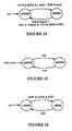
- Figure 14 shows the state diagram which determines the value of the signal ANHS1 (Acceptor NRFD Hold-off State 1);
- Figure 15 shows the state diagram which determines the value of the signal ANHS2 (Acceptor NRFD Hold-off State 2) ;
- Figure 16 shows the state diagram which determines the value of the signal AEHS (Acceptor END Hold-off State);
- Figure 17 shows the state diagram which determines the value of the signal CCHDF (Carry Cycle Holdoff Function). This state machine implements the last byte handling feature during read cycles with terminal count; and
- Figure 18 shows the state diagram which generates the GPIB bus signal EOI (END-OR-IDENTIFY).
-
- In the Figures and in the description below, the symbol "-" means a logical NOT, the symbol "+" means a logical OR, and the symbol "&" means a logical AND.
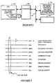
- Referring to Figure 1, there is shown a
controller interface 100 which couples amicroprocessor controller 102 to an IEEE 488bus 104, which in turn is coupled to one ormore devices 106, such as digital voltmeters, spectrum analyzers, oscilloscopes, or any other instrument which is designed to send and receive commands and messages via an IEEE 488 bus. Some aspects of the present invention assume that themicroprocessor 102 includes aDMA controller 108 which controls DMA data transfers and also outputs a "terminal count" signal TC for indicating the end of a particular data transfer sequence. - The IEEE 488
bus 104 is also called the "GPIB" (general purpose interface bus). - Whenever a signal or signal line name begins with the letter "N", it is a negative logic signal or signal line. To clarify the explanations herein, all signals will be described using positive signal logic terminology.
- Referring to Figure 2, the
controller interface 100 in accordance with an embodiment of the present invention includes two "ports": amicroprocessor port 120 and an IEEE 488bus 104. The preferred embodiment of the invention will be described from the viewpoint of having a microprocessor controller coupled toport 120 and a variety ofinstruments 106 coupled to the IEEE 488bus 104. However, it should be understood that thissame circuit 100 can be used to couple the microprocessor inside aninstrument 106 to the IEEE 488bus 104. Thus theinterface 100 is a general purpose circuit for coupling either an instrument or a controller to the IEEE 488bus 104. - The structure of the IEEE 488
bus 104 is shown in Figure 3. As shown, it has the following lines: - 1) an eight bit data bus.
- 2) an NRFD (not ready for data) line which is asserted so
as to temporarily prevent the assertion of new data on
the
bus 104. More specifically, the assertion of the DAV (data valid) signal is prevented. - 3) an DAV (data valid) line, which is asserted when a byte of data has been asserted on the bus.
- 4) an NDAC (not data accepted) line, which becomes logically true when the device receiving a byte of a message accepts the message. When several devices are reading a broadcast message, NDAC becomes true only when the slowest device has accepted delivery of the byte.
- 5) IFC (interface clear) line, which is asserted to reset a number of device interface functions (i.e., state machines in the interface).
- 6) ATN (attention) line, asserted by the controller before "addressing" one or more of the devices on the IEEE 488 bus. When ATN is asserted a device address is asserted on the data bus.
- 7) SRQ (service request) line, asserted by devices when they need to be serviced by the controller.
- 8) REN (remote enable) line, used by the controller to instruct devices on the IEEE 488 bus to begin responding to commands from the controller.
- 9) EOI (end or identify) line: "end" is used to mark the last byte in a multiline message, and "identify" is used by a controller when identifying devices requesting service.
-
-
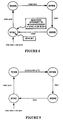
Microprocessor port 120 contains a set of addressable data registers 122-130 for defining the interface's mode of operation, and for storing commands and messages being transmitted to and from the IEEE 488bus 104. Referring to Figure 4, the data registers 122-130 inport 120 include an eight bit Command/Data Out Register (CDOR) 122 which is the general purpose register used for forwarding data, multiline messages, and commands from a controller to the IEEE 488bus 104. Similarly, there is an eight bit Data In Register (DIR) 123, which is used by themicroprocessor 102 to receive data and message bytes from other devices on the IEEE 488bus 104. TheKey Register 124 contains bit flags which specify the mode of communication with a microprocessor. Only the "200ns T1" bit is relevant to this embodiment of the present invention. - The control circuitry for the CDOR 122 a local message, 'nba' (new byte available), which is true whenever a new byte of data is written into the CDOR.
- The Auxiliary Registers B and I 126 and 128 are used for functions not normally required by the IEEE 488 standard, some of which will be described below. Another
register 130 stores SYNC and SYNC IE bits, described in more detail below. Other bits in thisauxiliary register 130 include the END bit, and the DI (data in) bit. The END bit is set whenever theinterface 100 accepts a message byte from a device on theGPIB 104 with the EOI line asserted, indicating that the last byte of a message has been sent. The DI bit is set whenever theinterface 100 accepts a message byte from a device on theGPIB 104. - Referring once again to Figure 2, the
microprocessor port 120 also includes aninstruction decoder 132 which decodes address, data and read/write signals from the microprocessor bus to generate local commands. The local command signals generated by thedecoder 132 which are relevant to this embodiment of the present invention include: cont (continuous mode), rddir (read data in register), wrodor (write to command/data out register), rdhf (release handshake holdoff), hlda (holdoff on all), hide (holdoff on end mode), hldi (holdoff immediate), holdoff (holdoff, i.e., stop transmission of further data), pon (power on reset), clear sync (clear SYNC bit to exit SYNC state), set sync (set SYNC bit), seoi (send EOI), and 'nbaf' (new byte available false) which resets the 'nba' (new byte available) signal generated by theCDOR 122. - There is a
SYNC state machine 140 used for detecting when the IEEE 488 bus handshake is synchronized. The SourceHandshake state machine 142 is used when "sourcing" messages or data to thebus 104. "Sourcing" means that data is being sent from the microprocessor to a device coupled to theGPIB 104. - The Acceptor
Handshake state machine 144 is used when accepting (i.e., receiving) multiline messages from a device on theGPIB 104. TheTalker state machine 146 is used to control the transmission of device specific messages to devices on theGPIB 104. TheListener state machine 148 is used to control the reception of device specific messages from devices on theGPIB 104. - The Service
Request state machine 150 asserts the signal SRQ on the IEEE 488 bus to request services from the active bus controller. - The
Controller state machine 160 determines when the SourceHandshake State Machine 142 is used to send interface messages (e.g., trigger, clear, and addressing messages) to devices on theGPIB 104. TheController state machine 160 also handles service requests by devices on theGPIB 104. - The state machines shown in Figure 2 are interconnected by internal busses and
signal lines 162 so that each state machine can use signals from the others. - Referring to Figures 5A and 5B, in accordance with the IEEE 488 standard, a data settling time of at least 350 nanoseconds (T1) is required before multiline messages or data sent by a controller are valid on the IEEE 488 bus. It should be noted that in some circumstances the T1 data settling time must be 500 nanoseconds or 2 microseconds, depending on the system configuration. Further, the first byte of each message requires additional settling time.
- Prior implementations of IEEE 488 interfaces begin counting this data settling time called T1, at the trailing edge of the controller's write strobe. However, in many circumstances, data is valid on the microprocessor's data bus for at least 150 nanoseconds before the trailing edge of its write strobe signal. Therefore, the speed of data communications can be improved by overlapping the T1 data settling time with the last 150 nanoseconds of the write strobe, at least in those circumstances where it is known that the data on the controller's bus is valid during that 150 nanosecond period.
- The preferred embodiment of the present invention takes advantage of this overlap by setting the 200ns T1 bit, which, when set, instructs the Source Handshake circuit to count only 200 nanoseconds after the trailing edge of the write strobe instead of 350 nanoseconds.
- By implementing the CDOR Register with a transparent latch, we are able to overlap the write of the CDOR with the required data setup on the GPIB (T1 delay). By overlapping, the time required to complete a GPIB transfer is reduced by the width of the overlap. This results in a faster transfer rate across the GPIB.
- Command/Data Out Register (CDOR). As shown in Figure 4, the Command/Data Out Register (CDOR) is an 8-bit write-only register used to move data from the computer to the
GPIB 104 when the interface is the GPIB Talker or the Active Controller. Outgoing data is separately latched by this register and is not destroyed by a read from the DIR (data in register). When a byte is written to the CDOR, the GPIB Source Handshake (SH) function is initiated (i.e., the local message 'nba' - new byte available - is true) and the byte is transferred to the GPIB. This register may also be written by a direct memory access (DMA) controller. The CDOR is a transparent latch, thus changes on the microprocessor's data bus during write cycles to the CDOR are reflected on the GPIB data bus. - Key Register (KEYR). The Key Register is a write-only register. The bit pattern of the KEYR is shown in Figure 4. When the 200ns T1 Delay bit is set by the microprocessor, the
interface circuit 100 generates a very short data settling time (200 nanoseconds) when theinterface 100 is used to source data onto theGPIB 104. - Auxiliary Register B (AUXRB). The TRI bit in AUXRB determines the interface circuit's Source Handshake Timing, T1. TRI can be set by the microprocessor to enable high speed data transfers (T1 >= 500 nsec) when tri-state GPIB drivers are used. Setting TRI enables high-speed timing as T1 of the Source Handshake after transmission of the first data byte. Clearing TRI enables low-speed timing (T1 >= 2 microseconds). The T1 delay can be reduced further by setting the VSTD bit in AUXRI or by setting the 200ns T1 bit in
KEY Register 124. - Setting the VSTD bit in AUXRI sets the value of the T1 delay used by the source handshake function for data setup to 350 nsec for the second and subsequent data bytes sent after ATN unasserts. If this bit is cleared, the value of T1 is determined by the TRI bit in AUXRB.
- Source Handshake (SH). The Source Handshake state machine differs from the state diagram shown in the IEEE 488.1 Specification. States SWNS and SIWS are removed. These states recorded the false transition of the local message new byte available ('nba'). The source handshake state diagram for the preferred embodiment is shown in Figure 6.
- Source Idle State (SIDS): In SIDS the Source Handshake function is disabled. The Source Handshake function powers on in SIDS and goes from SIDS to SGNS whenever the
interface 100 is in a state (Taken Active State(TACS), Serial Port Active State(SPAS), or Controller Active State(CACS)) where it needs to source bytes onto theGPIB 104. The Source Handshake function returns to SIDS within t2 if none of these states is active (t2 is specified and defined in IEEE Std 488.1). - Source Generate State (SGNS): In SGNS the
interface 100 is driving the CDOR onto the DIO lines of theGPIB 104, but is waiting for either a command byte, data byte, or serial port response to become available before issuing a new byte available ('nba') message. The Source Handshake function goes from SGNS to SDYS1 when the local message 'nba' becomes true. - Source Delay State 1 (SDYS1) : In SDYS the Source Handshake function is driving the new byte in the CDOR onto the DIO lines of the
GPIB 104 for a time of at least T1. The SH function leaves SDYS1 and enters SDYS2 after a time of T1 has elapsed. - Source Delay State 2 (SDYS2): In SDYS2 the DIO lines have already been driven with valid data for at least T1, and the SH function is waiting for all listeners to unassert NRFD (not ready for data) before asserting DAV (data valid). The SH function leaves SDYS2 and enters STRS as soon as no listeners are asserting NRFD.
- Source Transfer State (STRS): In STRS the SH function is asserting DAV, indicating that the data on the GPIB DIO lines is valid. The SH function leaves STRS and returns to SGNS once all listeners have unasserted NDAC (not data accepted).
- When 'nba' is true, the source handshake function transitions from SGNS to SDYS1.
- The source handshake function remains in SDYS1 driving the contents of the CDOR on the GPIB DIO lines for the amount of time specified by the T1 time delay. T1 is determined by the value of the TRI, VSTD and 200ns T1 bits and by HSTS (see Figure 7 and the following Table). HSTS is entered after the first data byte after ATN unasserts is sent. This enables a shorter bus settling time for all subsequent bytes until ATN becomes true. HSTS is always FALSE when the interface is the active controller (i.e., when ATN is asserted).
200ns T1 Bit TRI VSTD ∼HSTS T1 Delay for Commands and 1st Data Byte ∼HSTS T1 Delay for Subsequent Data Bytes 0 0 0 2.0 usec. 2.0 usec. 0 0 1 1.1 usec. 1.1 usec. 0 1 0 2.0 usec. 500 ns 0 1 1 1.1 usec. 350 ns 1 X X Same as above 200ns + width of overlap - Note that all the time values in the above chart are delay periods subsequent to the trailing edge of the write pulse. Thus, if TRI and VSTD are set and 200ns T1 is clear, there is still a 150ns overlap, plus 350ns delay after the trailing edge of the write pulse, which together meet the 500ns T1 delay required by the IEEE 488 specification.
- As shown in Figure 5B, this scheme is implemented by using a multiple
output time counter 180 which outputs five potential T1 trigger signals. Thecounter 180 is enabled only when the Source Handshake state machine (see Figure 6) is in the SDYS1 state. Asimple multiplexer 182 selects the proper signal one of these five signals, based on the values of the HSTS, TRI, VSTD and 200ns T1 signals, and outputs it as the T1 signal, which is used to transistion from SDYS1 to SDYS2 in the Source Handshake state machine. - After the amount of time specified by T1 has elapsed, SDYS2 is entered.
- A preferred embodiment of the present invention provides an enhancement to multibyte message processing by an IEEE 488 interface. More specifically, it provides a method of notifying the microprocessor, using an interrupt signal, that the last byte of an IEEE 488 message has been accepted by all listeners on the bus. To activate this enhanced function, the microprocessor writes a "1" into the SYNC IE (synchronization interrupt enable) bit of the
register 130, shown in Figure 4. When the SYNC IE bit is set, and the SYNC state machine (shown in Figure 2) enters the SYNC state, an interrupt signal is sent to the microprocessor, notifying it that the end of the message has been reached. - SYNC Function. The SYNC function is not defined in IEEE Std 488. It controls a special SYNC bit in the interface circuit, which indicates that the GPIB has synchronized at the end of a transfer (the GPIB is said to be synchronized when DAV is unasserted after the last byte transferred). The SYNC bit is set at the completion of a transfer when the GPIB handshaking is complete.
- The SYNC function may actually be implemented as one state machine with very complex terms for its transitions, but since its usage is substantially different for DMA (direct memory access) reads, DMA writes, programmed I/O reads, and programmed I/O writes, four separate state diagrams are presented in the Figures. In all cases, the SYNC bit is set only in the SYNC state. Furthermore, an interrupt is generated (for prompting the microprocessor) only if the SYNC bit is set and the microprocessor has previously set the SYNC IE bit.
- Programmed I/O Write SYNC Function. The state diagram for the programmed I/O write version of the SYNC state machine is shown in Figure 8. For the SYNC state machine to be in this mode the interface circuit must be in TACS (talker active state) or CACS (controller active state), and must not be using DMA for sourcing messages.
- Synchronized State (SYNC): In SYNC, the
interface 100 is done with its current data transfer, the GPIB is synchronized, and the SYNC bit is set. The state machine exits SYNC and goes to WCWS if the SYNC bit is cleared (a 'clear sync' pulse is issued.) The microprocessor's driver software should issue a 'clear sync' command, which causes the interface to generate a 'clear sync' pulse that clears the SYNC bit before writing the last data byte of a programmed I/O transfer to the CDOR. - Write Cycle Wait State (WCWS): In WCWS the 'clear sync' pulse is true, but the state machine is waiting for the 'clear sync' pulse to become false. The state machine goes from WCWS to DVWS as soon as the 'clear sync' pulse becomes false.
- Data Valid Wait State (DVWS): In DVWS the state machine is waiting for the byte to be sourced. The state machine exits DVWS and enters WSNS when DAV (data valid) is asserted (the last byte is being sourced).
- Wait for Synchronization State (WSNS): In WSNS, DAV is asserted for that last byte of the transfer and the state machine is waiting for DAV to unassert before setting the SYNC bit. The state machine returns to the SYNC state when DAV becomes false.
- DMA Writes SYNC Function. The state diagram for the SYNC state machine during DMA writes is shown in Figure 9. For the SYNC state machine to be in this mode the interface must be in TACS or CACS.
- Synchronized State (SYNC): In SYNC, the interface is done with its current data transfer, the GPIB is synchronized, and the SYNC bit is set. The SYNC state machine exits SYNC and goes to TCWS if a 'clear sync' command is issued. The driver software should clear the SYNC bit before beginning a DMA write operation.
- Terminal Count Wait State (TCWS): In the TCWS state, the SYNC state machine is waiting for a DMA write access to the CDOR with TC (terminal count) asserted (when the last byte of the DMA transfer is written to the CDOR). The SYNC state machine goes from TCWS to DVWS as soon as the DMA controller in the microprocessor writes the last byte of the message to the CDOR (as indicated by the TC signal).
- Data Valid Wait State (DVWS): In DVWS the last byte has been written to the CDOR and the SYNC state machine is waiting for the byte to be sourced. The SYNC state machine exits DVWS and enters WSNS when DAV is asserted (the last byte is being sourced).
- Wait for Synchronization State (WSNS): In WSNS, DAV is asserted and the SYNC state machine is waiting for DAV to unassert before setting the SYNC bit. The SYNC state machine returns to the SYNC state when DAV becomes false.
- For the SYNC function to be useful during DMA write operations the DMA controller must be capable of asserting the TC signal during the write cycle of the last byte to the CDOR.
- Programmed I/O Reads SYNC Function. The state diagram for the SYNC state machine during programmed I/O reads is shown in Figure 10. For the SYNC state machine to be in this mode the interface must be in LACS (listener active state).
- Sync State (SYNC): In SYNC, the
interface 100 is done with its current data transfer, the GPIB is synchronized, and the SYNC bit is set. The SYNC state machine exits SYNC and goes to WSNS when DAV is asserted. - Wait for Synchronization State (WSNS): In WSNS, DAV is asserted. The SYNC state machine returns to SYNC if DAV is unasserted. Note that during a programmed I/O read, the SYNC bit is set when DAV is false and cleared when DAV is true.
- The SYNC bit will toggle with every byte during programmed I/O reads, therefore, the SYNC bit should not be polled or enabled for interrupts until after reading the last byte of a transfer from the DIR. The 'clear sync' command should not be issued during programmed I/O reads.
- DMA Reads SYNC Function. The state diagram for the SYNC state machine during DMA reads is shown in Figure 11. For the SYNC state machine to be in this mode the interface must be in LACS.
- Sync State (SYNC): In SYNC, the
interface 100 is done with its current data transfer, the GPIB is synchronized, and the SYNC bit is set. The SYNC state machine exits SYNC and goes to WCWS if the SYNC bit is cleared (the 'clear sync' command is issued). The driver software should clear the SYNC bit before beginning a DMA transfer. - Write Cycle Wait State (WCWS): In WCWS the 'clear sync' pulse is true, but the SYNC state machine is waiting for the 'clear sync' pulse to become false. The SYNC state machine goes from WCWS to WSNS as soon as the 'clear sync' pulse is false.
- Wait for Synchronization State (WSNS): In WSNS, the 'clear sync' pulse has been received and DAV is asserted. The SYNC state machine leaves WSNS and enters SYNS when DAV unasserts.
- Synchronization State (SYNS): In SYNS the GPIB is synchronized (DAV is not asserted). The SYNC state machine exits SYNS and enters WSNS if DAV is asserted. If LBRS is active (which means that the last byte of the DMA transfer has been read by the DMA controller), the SYNC state machine exits SYNS and returns to SYNC.
- Not Last Byte Read State (~LBRS): In ~LBRS the SYNC state machine is waiting for the DMA controller to read the last byte of the DMA transfer. The SYNC state machine exits -LBRS and enters LBRS when the 'set sync' command is issued or the DIR was read via a (DMA Controller). DACK access while TC (terminal count) is true.
- Last Byte Read State (LBRS): In LBRS the last byte of the DMA transfer has been read from the DIR or the set sync command has been issued. The SYNC state machine exits LBRS and returns to ~LBRS when the processor issues a 'clear SYNC' command.
- Once started the SYNC function will toggle between WSNS and SYNS for each byte. While in SYNS the function will transfer to SYNC if LBRS is true. This will happen automatically if terminal count is reached while reading the last byte from the DIR (data input register). However, if this does not happen (i.e. a time-out or early END is detected) then LBRS can be set by issuing the 'set sync' command, which will cause the SYNC bit to set (i.e., the GPIB is synchronized).
- IEEE std 488 defines a local message, rfd (ready for data), which is issued before each byte of data is received by the microprocessor. The 'rfd' message is transmitted on the NRFD line of the bus (see Figure 3). Issuance of this local message affects GPIB signal lines in such a way as to permit the talker to send the next data byte over the GPIB. In order to achieve maximum data transmission rates, this local message is asserted automatically during a data transfer cycle whenever the interface is ready to receive another byte.
- After the last byte of a data transfer, however, it is necessary for the microprocessor to inhibit the local 'rfd' message, thereby preventing the talking device from sending further bytes. For example, if the application running in the microprocessor requested to read 100 bytes from a device, and for some reason the device had more than 100 bytes to send, transmission of the 101st byte must be inhibited until the application specifically requests more bytes. Since at the moment when the 100 bytes have been received it is unknown to the microprocessor whether the application needs or wants further bytes, or whether the application intends to cause subsequent bus activity, the safest course is to inhibit the arrival of further bytes.
- In order to block the arrival of further bytes, prior art devices have required software intervention between the next-to-last and last bytes of a transfer, effectively instructing the interface to fail to issue the 'rfd' local message after the next (i.e., last) byte is received. This software is not only detrimental to system performance, but greatly increases the complexity of the driver software controlling the interface. It requires that all incoming data transfers be broken into two parts: the first n-1 bytes are to be transferred as a group, usually by DMA, followed by a second transfer of one byte. Between the two transfers, the software in the microprocessor instructs the interface to fail to issue the standard 'rfd' message. In addition to the complexity of breaking up a transfer, there are asynchronous GPIB events (such as incoming END messages) which may occur between the two parts, and which cause various race conditions which, using prior art devices alone, can require extremely complex software to avoid.
- This embodiment of the present invention alleviates the need for this software intervention by allowing the last-byte 'rfd' inhibition commands to be pre-programmed before the entire transfer begins. The entire transfer may then occur without the need to break it up, and the interface will correctly program itself before the last byte to inhibit the 'rfd' message. This feature, therefore, increases throughput and greatly decreases software complexity by eliminating the software intervention previously required by prior art devices.
- A similar situation exists for write operations (data being transmitted to a device over the GPIB). Before the last byte is sent, the IEEE 488 interface must be programmed to send the END message along with the last byte by asserting the EOI line of the GPIB. In order to accomplish this programming with prior art interfaces, software intervention was required as described above, and similar decreases in throughput and increases in software complexity are experienced. With this embodiment, however, this last-byte programming can be set up in advance, allowing the entire transfer to occur with no software intervention.
- The direct memory access (DMA) controller in a microprocessor contains a counter that is used to determine when the last word or byte of a DMA transfer has been reached. The DMA controller outputs a signal, herein called TC, which is asserted when the DMA controller's counter reaches the value for the last word or byte to be read or written by the microprocessor. As will be described below, this TC signal is used by the present invention to trigger a handshake holdoff when data is being accepted from the GPIB, and to trigger the generation of an END message when data is being sourced to the GPIB.
- Setting the ACC bit enables automatic carry cycles on GPIB DMA transfers. When the ACC bit is set during GPIB DMA reads, the acceptor handshake function will perform a RFD (ready for data) holdoff on the last byte read by the DMA controller (that is, the byte in which the TC signal is pulsed when read). Issuing the 'Finish Handshake' auxiliary command releases the holdoff.
- Acceptor Handshake. The Acceptor Handshake state diagram for the IEEE 488
interface 100 is shown in Figure 12. The following chart lists the outputs and actions of each of the acceptor handshake states.STATE RFD DAC Other Actions AIDS (T) (T) Acceptor Handshake is idle ANRS F F RFD Holdoff State ACRS (T) F Ready To Accept Data State ADYS F F If ATN is false - latch data into the DIR - set the DI (Data In) bit and END bit if appropriate If ATN is true - commands decoded and appropriate interrupts set - SDHS set if commands require DAC (data accepted) holdoff ACDS F F DAC Holdoff State AWNS F (T) Waiting for DAV to unassert (new cycle to begin) - The implementation of the Acceptor Handshake in the present invention differs from the state diagram shown in the IEEE 488.1 Specification. The IEEE 488.1 state ACDS is divided into two states ADYS and ACDS. ADYS is entered after DAV is asserted and is the state in which data is strobed into the DIR and action is taken on the reception of GPIB commands. All interrupt status bits generated by the acceptor handshake are set by this state. The ACDS state is entered one clock cycle (Tah2) after ADYS is entered and is used as a holding state where the device will remain during DAC (data accepted) holdoffs. ANRS is the RFD holdoff state. To release the RFD holdoff either ATN must be asserted or the local message 'rdy' must be cleared. The 'rdy' local message is defined as:
- If the acceptor handshake function is in ACRS and ATN is false, issuing a 'rhdf' or 'hldi' command or reading the DIR (rddir) causes a transition to ANRS. This transition is NOT permitted by the IEEE 488 specification. Therefore it is the responsibility of the control program not to perform the actions mentioned above while in ACRS.
- The Acceptor Handshake state machine uses five more state diagrams to implement the acceptor handshake function. The ADHS state diagram shown in Figure 13 is used to perform DAC holdoffs. ADHS is set if a command is received that the
interface circuit 100 has been configured to perform a DAC holdoff (represented by SDHS in the state diagram). When ATN is asserted and ADHS is true the acceptor handshake will remain in ACDS until ADHS or ATN go false. The DAC holdoff can be released by issuing the 'valid' or 'nonvalid' commands which clears ADHS. Figure 13 shows the state diagram of the DAC Holdoff function. - Four separate state diagrams (ANHS1&2, AEHS and CCHDF) are implemented to perform RFD holdoffs. ANHS1 (shown in Figure 14) is set in ADYS when ATN is false. ANHS1 indicates that a data byte was received and a RFD holdoff will occur to prevent the next data byte from being sent. The holdoff will be released when the data byte is read from the DIR unless one of several special holdoff conditions are enabled. The special holdoff conditions (represented by holdoff in the state diagram) include holdoff on all (hlda) mode, continuous (cont) mode, holdoff on end (hide) mode and AEHS set, ANHS2, or CCHDF. If one of the special holdoff conditions is set then a release handshake holdoff (rhdf) auxiliary command must be issued to release the RFD holdoff. Where:
- The ANHS2 state diagram shown in Figure 15 is used to holdoff the handshake immediately. ANHS2 is set by issuing the 'holdoff immediately' (hldi) auxiliary command and is cleared by issuing the 'release handshake holdoff' (rhdf) command. ANHS2 is not cleared by a 'pon' (power on reset), therefore it allows the control program to issue a 'holdoff immediately' (hldi) command while 'pon' is set and the interface circuit is being configured.
- The AEHS state diagram (shown in Figure 16) is implemented to record the reception of an END condition and allow a RFD holdoff to be performed afterward. AEHS is set on the reception of an END condition (i.e., when the last byte of the message is received) and is cleared when a 'release handshake holdoff' (rhdf) command is issued.
- The Carry Cycle Holdoff State Diagram (shown in Figure 17) is implemented to record the occurrence of a DMA Read of the DIR (rddir) with TC asserted and allows a RFD holdoff to be performed afterward if the automatic carry cycle bit (ACC) is set. CCHDF is cleared when the ACC bit is cleared or ANHS1 is false.
- EOI Generation Function. The EOI Generation state diagram is shown in Figure 18. The EOI Generation state diagram is used to control the assertion of EOI by the interface while sourcing a data byte. If the 'Send EOI' auxiliary command (seoi) is issued followed by a write of the CDOR (wrcdor) while the interface is in TACS (talker active state), the EOI Generation state machine will enter ERAS and assert the GPIB EOI line. The function will enter ENAS as soon as the source handshake enters SDYS1 + SDYS2. EOI will remain asserted while in (ERAS or ENAS) and in (SYDS or STRS). If it is desired to send EOI with the next byte, then 'seoi' must be issued before the CDOR is written to return the function to ERAS. The next write to the CDOR (wrcdor) will cause the function to enter ENIS.
- The auxiliary command 'nbaf' (new byte available false) and the local message 'pon' always clear the EOI Generation function, forcing it into its idle state, ENIS.
- When the automatic carry cycle feature is enabled (ACC = 1) the EOI generation function will make the transition from ENIS to ENRS or ENAS to ERAS when the CDOR is written (wrcdor) with the TC signal asserted while in TACS. This will cause EOI to assert while sending the GPIB data written to the CDOR.
- Further aspects of the present invention are as follows.
- In one aspect, the present invention provides a bus interface which couples a microprocessor to an IEEE 488 bus, the interface comprising: a microprocessor port which transmits and receives data to and from a microprocessor; said microprocessor port including microprocessor data bus lines and a write line for receiving write pulses from said microprocessor; each said write pulses having a predefined duration and a trailing edge; an IEEE 488 bus; said IEEE 488 bus including data lines and a data valid (DAV) line; talker circuit means, coupled to said microprocessor port and said IEEE 488 bus, for asserting data received by said microprocessor port onto said IEEE 488 bus; and source handshake means, coupled to said talker circuit means and said IEEE 488 bus, for asserting a signal on said DAV line of said IEEE 488 bus after said talker circuit has asserted data on said IEEE 488 bus for a predefined settling period; said source handshake means including overlap means for beginning said predefined settling period a predefined amount of time before said trailing edge of each said write pulse; whereby speed of transmission of data by said microprocessor is improved by overlapping a portion of said write pulse with said predefined settling period.
- In one embodiment, the interface includes an overlap enable switch for enabling said overlap means; said talker circuit beginning said predefined settling period at the trailing edge of each said write pulse when said overlap enable switch is not enabled.
- According to another aspect, the present invention provides a bus interface which couples a microprocessor having a direct memory access controller to an IEEE 488 bus, the interface comprising: a microprocessor port which transmits and receives data to and from a microprocessor having a direct memory access controller which generates a terminal count (TC) signal upon transmission of the last datum in a multiple datum data transfer; said microprocessor port including microprocessor data bus lines and a terminal count line for receiving said TC signals from said direct memory access controller; an IEEE 488 bus; said IEEE 488 bus including data lines and an END-OR-IDENTIFY (EOI) line; talker circuit means, coupled to said microprocessor port and said IEEE 488 bus, for asserting (sourcing) data received by said microprocessor port onto said IEEE 488 bus; and source handshake means, coupled to said talker circuit means and said IEEE 488 bus, for asserting an END signal on said EOI line of said IEEE 488 bus when said microprocessor port receives a TC signal from said direct memory access controller and said talker circuit asserts data on said IEEE 488 bus; whereby an END signal is automatically transmitted with the last byte of each DMA data transfer sourced by said interface onto said IEEE 488 bus.
- In another aspect, the present invention provides a bus interface which couples a microprocessor having a direct memory access controller to an IEEE 488 bus, the interface comprising: a microprocessor port which transmits and receives data to and from a microprocessor; said microprocessor port having an interrupt signal port; said microprocessor port including at least one line for transmitting interrupt signals to said interrupt signal port of said microprocessor; an IEEE 488 bus; said IEEE 488 bus including data lines and an END-OR-IDENTIFY (EOI) line and a NOT READY FOR DATA (NRFD) line; listener circuit means, coupled to said microprocessor port and said IEEE 488 bus, for transmitting data from said IEEE 488 bus to said microprocessor via said microprocessor port; and acceptor handshake means, coupled to said listener circuit means and said IEEE 488 bus, for detecting when an END signal is asserted on said EOI line of said IEEE 488 bus while said listener circuit means is transmitting data to said microprocessor via said microprocessor port and for then transmitting an interrupt signal to said interrupt signal port of said microprocessor via said microprocessor port; whereby said microprocessor is automatically notified by said interrupt signal that the last byte of a data transfer has been transmitted by said interface from said IEEE 488 bus to said microprocessor.
- In one embodiment, the interface includes a synchronization interrupt enable switch for enabling said acceptor handshake means to send interrupt signals to said microprocessor; wherein said acceptor handshake means does not send an interrupt signal at the end of a data transfer to said microprocessor unless said synchronization interrupt enable switch is enabled.
- In another aspect, the present invention provides a bus interface which couples a microprocessor having a direct memory access controller to an IEEE 488 bus, the interface comprising: a microprocessor port which transmits and receives data to and from a microprocessor having a direct memory access controller which generates a terminal count (TC) signal upon transmission of the last datum in a multiple datum data transfer; said microprocessor port including microprocessor data bus lines and a terminal count line for receiving said TC signals from said direct memory access controller; an IEEE bus; said IEEE 488 bus including data lines and a NOT READY FOR DATA (NRFD) line; listener circuit means, coupled to said microprocessor port and said IEEE 488 bus, for transmitting data from said IEEE 488 bus to said microprocessor via said microprocessor port; and acceptor handshake means, coupled to said listener circuit means and said IEEE 488 bus, for asserting a hold off signal on said NRFD line of said IEEE 488 bus when said microprocessor port receives a TC signal from said direct memory access controller while said listener circuit transmits data from said IEEE 488 bus to said microprocessor via said microprocessor port; whereby said acceptor handshake means automatically performs a data hold off upon transmission of the last datum in a multiple datum DMA data transfer from said IEEE 488 bus to said microprocessor.
Claims (7)
- A bus interface that couples a microprocessor to an IEEE 488 bus, the interface comprising:characterized by:a microprocessor port (120) that transmits and receives data to and from the microprocessor; said microprocessor port including microprocessor data bus lines and a write line for receiving write pulses from said microprocessor; each said write pulses having a predefined duration and a trailing edge;an IEEE 488 bus (104); said IEEE 488 bus (104) including data lines and a data valid (DAV) line;talker circuit means, coupled to said microprocessor port (120) and said IEEE 488 bus (104), including a transparent latch for asserting and latching data received by said microprocessor port (120) onto said IEEE 488 bus (104) such that data received from said microprocessor port (120) is asserted onto said IEEE 488 bus (104) before the trailing edge of said write pulses; andsource handshake means, coupled to said talker circuit means and said IEEE 488 bus (104), for asserting a signal on said DAV line of said IEEE 488 bus (104) after said talker circuit has asserted data on said IEEE 488 bus (104) for a first predefined minimum settling time;said source handshake means including speedup means that, when enabled, asserts said signal on said DAV line of said IEEE 488 bus (104) after said talker circuit has asserted data on said IEEE 488 bus (104) for a second predefined settling time that is less than said first predefined minimum settling time;whereby speed of transmission of data by said microprocessor is improved by reducing said settling time.
- The bus interface of claim 1, further characterized by:
a speedup enable switch for enabling said speedup means. - The bus interface of claim 1 or 2, further characterized by:whereby said acceptor handshake means (144) automatically performs a data hold off upon transmission of any specified datum in a multiple datum DMA data transfer from said IEEE 488 bus (104) to said microprocessor (102).said IEEE 488 bus (104) including NOT READY FOR DATA (RFD) line; listener circuit means, coupled to said microprocessor port (120) and said IEEE 488 bus (104), for transmitting data from said IEEE 488 bus (104) to said microprocessor via said microprocessor port (120); andacceptor handshake means (144), coupled to said listener circuit means and said IEEE 488 bus (104);said microprocessor having a direct memory access controller (108) that generates a terminal count (TC) signal upon transmission of any specified datum in a multiple datum data transfer; said microprocessor port (120) including microprocessor data bus lines and a terminal count line for receiving said TC signals from said direct memory access controller (108); andsaid acceptor handshake means (144) including means for asserting a hold off signal on said RFD line of said IEEE 488 bus (104) when said microprocessor port (120) receives a TC signal from said direct memory access controller (108) until a predefined condition is met;
- The bus interface of claim 3, further that said IEEE 488 bus (104) has completed the data transfer.
- A method of operating a bus interface that couples a microprocessor to an IEEE 488 bus, the steps of the method comprising:characterized by:transmitting and receiving data to and from the microprocessor via a microprocessor port that includes microprocessor data bus lines and a write line for receiving write pulses from the microprocessor; each of the write pulses having a predefined duration and a trailing edge;asserting and latching data received by said microprocessor port (120) onto data lines of an IEEE 488 bus (104) utilizing a transparent latch such that data received from said microprocessor port (120) is asserted onto said IEEE 488 bus (104) before the trailing edge of said write pulses; andasserting a signal on a DAV line of said IEEE 488 bus (104) after data has been asserted on the data lines of said IEEE 488 bus (104) for a first predefined minimum settling time;enabling a source handshake speedup mode of operation;when the source handshake speedup mode of operation is enabled, asserting said signal on said DAV line of said IEEE 488 bus (104) after data has been asserted on the data lines of said IEEE 488 bus (104) for a second predefined settling time that is less than said first predefined minimum settling time;whereby speed of transmission of data by said microprocessor is improved by reducing said settling time.
- The method of claim 5, further characterized by:transmitting data from said IEEE 488 bus (104) to said microprocessor via said microprocessor port (120) ;the microprocessor including a direct memory access controller that generates a terminal count (TC) signal upon transmission of any specified datum in a multiple datum data transfer; andasserting a hold off signal on a NRFD (Not Ready For Data) line of said IEEE 488 bus (104) when said microprocessor port (120) receives the TC signal from the direct memory access controller (108) of said microprocessor, and continuing to assert said hold off signal until a predefined condition is met; whereby a data hold off is automatically performed upon transmission of any specified datum in a multiple datum DMA data transfer from said IEEE 488 bus (104) to said microprocessor (102).
- The method of claim 6, further characterized by:detecting when the last byte of a data transfer has been received from said IEEE 488 bus (104) while data is being transmitting to said microprocessor via said microprocessor port (120), and then transmitting a first interrupt signal to said microprocessor via said microprocessor port (120); anddetecting when a data valid signal previously asserted on said DAV line is unasserted, and then transmitting a second interrupt signal to said microprocessor via said microprocessor port (120);whereby said microprocessor is automatically notified by said first interrupt signal that the last byte of a data transfer has been transmitted by said interface from said IEEE 488 bus (104) to said microprocessor and said microprocessor is automatically notified by said second interrupt signal that said IEEE 488 bus (104) has completed the data transfer.
Applications Claiming Priority (3)
| Application Number | Priority Date | Filing Date | Title |
|---|---|---|---|
| US07/548,293 US5287528A (en) | 1990-07-03 | 1990-07-03 | IEEE 488 interface for message handling method |
| US548293 | 1990-07-03 | ||
| EP91305995A EP0465221B1 (en) | 1990-07-03 | 1991-07-02 | IEEE 488 Interface |
Related Parent Applications (2)
| Application Number | Title | Priority Date | Filing Date |
|---|---|---|---|
| EP91305995.2 Division | 1991-07-02 | ||
| EP91305995A Division EP0465221B1 (en) | 1990-07-03 | 1991-07-02 | IEEE 488 Interface |
Publications (2)
| Publication Number | Publication Date |
|---|---|
| EP0805400A1 EP0805400A1 (en) | 1997-11-05 |
| EP0805400B1 true EP0805400B1 (en) | 2001-10-24 |
Family
ID=24188208
Family Applications (2)
| Application Number | Title | Priority Date | Filing Date |
|---|---|---|---|
| EP97110553A Expired - Lifetime EP0805400B1 (en) | 1990-07-03 | 1991-07-02 | IEEE488 interface and message handling method |
| EP91305995A Expired - Lifetime EP0465221B1 (en) | 1990-07-03 | 1991-07-02 | IEEE 488 Interface |
Family Applications After (1)
| Application Number | Title | Priority Date | Filing Date |
|---|---|---|---|
| EP91305995A Expired - Lifetime EP0465221B1 (en) | 1990-07-03 | 1991-07-02 | IEEE 488 Interface |
Country Status (4)
| Country | Link |
|---|---|
| US (2) | US5287528A (en) |
| EP (2) | EP0805400B1 (en) |
| JP (1) | JP3377798B2 (en) |
| DE (2) | DE69132786T2 (en) |
Families Citing this family (17)
| Publication number | Priority date | Publication date | Assignee | Title |
|---|---|---|---|---|
| AU5990194A (en) * | 1993-05-10 | 1994-12-12 | Taligent, Inc. | Audio synchronization system |
| JP3608804B2 (en) * | 1993-05-14 | 2005-01-12 | 株式会社ソニー・コンピュータエンタテインメント | Bus control device |
| US5572525A (en) * | 1995-05-31 | 1996-11-05 | National Instruments Corporation | GPIB extender with find listener protocol capabilities |
| US5649123A (en) * | 1995-06-07 | 1997-07-15 | National Instruments Corporation | GPIB system with improved parallel poll response detection |
| US5649129A (en) * | 1995-06-07 | 1997-07-15 | National Instruments Corporation | GPIB system including controller and analyzer |
| US6256660B1 (en) * | 1997-04-08 | 2001-07-03 | International Business Machines Corporation | Method and program product for allowing application programs to avoid unnecessary packet arrival interrupts |
| US6167480A (en) * | 1997-06-25 | 2000-12-26 | Advanced Micro Devices, Inc. | Information packet reception indicator for reducing the utilization of a host system processor unit |
| US10820949B2 (en) | 1999-04-07 | 2020-11-03 | Intuitive Surgical Operations, Inc. | Medical robotic system with dynamically adjustable slave manipulator characteristics |
| US6594552B1 (en) * | 1999-04-07 | 2003-07-15 | Intuitive Surgical, Inc. | Grip strength with tactile feedback for robotic surgery |
| US6831926B1 (en) | 2000-10-27 | 2004-12-14 | The Boeing Company | Legacy signals databus adapter/coupler |
| US6567966B2 (en) * | 2001-02-14 | 2003-05-20 | Agilent Technologies, Inc. | Interweaved integrated circuit interconnects |
| US7594026B1 (en) * | 2001-04-25 | 2009-09-22 | Zarlink Semiconductor (U.S.) Inc. | Method and apparatus for multi-phy communication without an ATM bus master |
| US6898723B2 (en) * | 2002-04-01 | 2005-05-24 | Mitac International Corp. | Method for verifying clock signal frequency of computer sound interface that involves checking whether count value of counter is within tolerable count range |
| US7005846B2 (en) * | 2002-07-17 | 2006-02-28 | Agilent Technologies, Inc. | System and method for application control in measurement devices |
| EP2341445B1 (en) * | 2009-12-30 | 2017-09-06 | Intel Deutschland GmbH | Method for high speed data transfer |
| EP2434404B1 (en) * | 2010-09-27 | 2017-08-23 | Intel Deutschland GmbH | Method and arrangement for streaming data profiling |
| US11030903B2 (en) * | 2018-05-30 | 2021-06-08 | Ford Global Technologies, Llc | Vehicle-to-infrastructure communication |
Family Cites Families (8)
| Publication number | Priority date | Publication date | Assignee | Title |
|---|---|---|---|---|
| US4319338A (en) * | 1979-12-12 | 1982-03-09 | Allen-Bradley Company | Industrial communications network with mastership determined by need |
| US4402055A (en) * | 1981-01-27 | 1983-08-30 | Westinghouse Electric Corp. | Automatic test system utilizing interchangeable test devices |
| US4396995A (en) * | 1981-02-25 | 1983-08-02 | Ncr Corporation | Adapter for interfacing between two buses |
| US4534011A (en) * | 1982-02-02 | 1985-08-06 | International Business Machines Corporation | Peripheral attachment interface for I/O controller having cycle steal and off-line modes |
| US4523310A (en) * | 1983-01-28 | 1985-06-11 | Gould Computer Systems Inc. | Synchronous communications multiplexer |
| US4680788A (en) * | 1983-08-31 | 1987-07-14 | Data General Corporation | Microprocessor based control and switching device |
| US4727370A (en) * | 1985-12-17 | 1988-02-23 | Ampex Corporation | Method and system for synchronous handshake generation |
| US4982325A (en) * | 1988-03-18 | 1991-01-01 | At&T Bell Laboratories | Applications processor module for interfacing to a database system |
-
1990
- 1990-07-03 US US07/548,293 patent/US5287528A/en not_active Expired - Lifetime
-
1991
- 1991-07-02 EP EP97110553A patent/EP0805400B1/en not_active Expired - Lifetime
- 1991-07-02 DE DE69132786T patent/DE69132786T2/en not_active Expired - Lifetime
- 1991-07-02 DE DE69128985T patent/DE69128985T2/en not_active Expired - Lifetime
- 1991-07-02 EP EP91305995A patent/EP0465221B1/en not_active Expired - Lifetime
- 1991-07-03 JP JP16259991A patent/JP3377798B2/en not_active Expired - Lifetime
-
1993
- 1993-11-18 US US08/154,867 patent/US5572684A/en not_active Expired - Lifetime
Also Published As
| Publication number | Publication date |
|---|---|
| DE69132786D1 (en) | 2001-11-29 |
| JPH05181790A (en) | 1993-07-23 |
| DE69132786T2 (en) | 2002-05-08 |
| EP0465221A2 (en) | 1992-01-08 |
| EP0465221B1 (en) | 1998-03-04 |
| US5287528A (en) | 1994-02-15 |
| EP0805400A1 (en) | 1997-11-05 |
| DE69128985T2 (en) | 1998-09-10 |
| JP3377798B2 (en) | 2003-02-17 |
| EP0465221A3 (en) | 1993-02-24 |
| DE69128985D1 (en) | 1998-04-09 |
| US5572684A (en) | 1996-11-05 |
Similar Documents
| Publication | Publication Date | Title |
|---|---|---|
| EP0805400B1 (en) | IEEE488 interface and message handling method | |
| EP0009678B1 (en) | Computer input/output apparatus | |
| US6823412B2 (en) | System and method for arbitration of a plurality of processing modules | |
| US6173349B1 (en) | Shared bus system with transaction and destination ID | |
| US4631670A (en) | Interrupt level sharing | |
| US5812875A (en) | Apparatus using a state device and a latching circuit to generate an acknowledgement signal in close proximity to the request signal for enhancing input/output controller operations | |
| JPH02227765A (en) | Data transfer apparatus for digital computer | |
| US5159684A (en) | Data communication interface integrated circuit with data-echoing and non-echoing communication modes | |
| US5475846A (en) | Apparatus for processing PCMCIA interrupt requests | |
| EP0030978B1 (en) | Data-transfer controlling system | |
| US4120029A (en) | Method and apparatus for recovering a signal transferred over a common bus in a data processing system | |
| US5315706A (en) | High speed IEEE 488 bus interface system and method | |
| US5608883A (en) | Adapter for interconnecting single-ended and differential SCSI buses to prevent `busy` or `wired-or` glitches from being passed from one bus to the other | |
| JPS58502027A (en) | Peripherals adapted to monitor low data rate serial input/output interfaces | |
| US5694586A (en) | Controller using time-domain filter connected to a signal line to control a time at which signal line is sampled for receipt of information transfer signal | |
| US5964853A (en) | Interface controller including hardware mechanism to handle PS/2 interface | |
| US6026455A (en) | Architecture and method for providing guaranteed access for a retrying bus master to a data transfer bridge connecting two buses in a computer system | |
| WO1988004808A1 (en) | Data transfer circuit | |
| EP0577110A2 (en) | Dual bus local area metwork interfacing system | |
| US6418491B1 (en) | Apparatus and method for controlling timing of transfer requests within a data processing apparatus | |
| US6408353B1 (en) | Microcomputer having sampling function of retry requesting signal in syncronization with strobe signal | |
| US5428797A (en) | Circuitry for eliminating bus contention at high frequencies by driving a bus to an available state prior to its relinquishing control of the bus | |
| RU2018944C1 (en) | Device for interfacing computer with external objects | |
| US20020099890A1 (en) | Apparatus and method for processing interruptions in a data transmission over a bus | |
| JP2842639B2 (en) | Data transfer method |
Legal Events
| Date | Code | Title | Description |
|---|---|---|---|
| PUAI | Public reference made under article 153(3) epc to a published international application that has entered the european phase |
Free format text: ORIGINAL CODE: 0009012 |
|
| AC | Divisional application: reference to earlier application |
Ref document number: 465221 Country of ref document: EP |
|
| AK | Designated contracting states |
Kind code of ref document: A1 Designated state(s): DE FR GB |
|
| 17P | Request for examination filed |
Effective date: 19980306 |
|
| 17Q | First examination report despatched |
Effective date: 20000220 |
|
| GRAG | Despatch of communication of intention to grant |
Free format text: ORIGINAL CODE: EPIDOS AGRA |
|
| GRAG | Despatch of communication of intention to grant |
Free format text: ORIGINAL CODE: EPIDOS AGRA |
|
| GRAH | Despatch of communication of intention to grant a patent |
Free format text: ORIGINAL CODE: EPIDOS IGRA |
|
| GRAH | Despatch of communication of intention to grant a patent |
Free format text: ORIGINAL CODE: EPIDOS IGRA |
|
| GRAA | (expected) grant |
Free format text: ORIGINAL CODE: 0009210 |
|
| AC | Divisional application: reference to earlier application |
Ref document number: 465221 Country of ref document: EP |
|
| AK | Designated contracting states |
Kind code of ref document: B1 Designated state(s): DE FR GB |
|
| REF | Corresponds to: |
Ref document number: 69132786 Country of ref document: DE Date of ref document: 20011129 |
|
| REG | Reference to a national code |
Ref country code: GB Ref legal event code: IF02 |
|
| ET | Fr: translation filed | ||
| PLBE | No opposition filed within time limit |
Free format text: ORIGINAL CODE: 0009261 |
|
| STAA | Information on the status of an ep patent application or granted ep patent |
Free format text: STATUS: NO OPPOSITION FILED WITHIN TIME LIMIT |
|
| 26N | No opposition filed | ||
| PGFP | Annual fee paid to national office [announced via postgrant information from national office to epo] |
Ref country code: GB Payment date: 20100630 Year of fee payment: 20 Ref country code: FR Payment date: 20100805 Year of fee payment: 20 Ref country code: DE Payment date: 20100630 Year of fee payment: 20 |
|
| REG | Reference to a national code |
Ref country code: DE Ref legal event code: R071 Ref document number: 69132786 Country of ref document: DE |
|
| REG | Reference to a national code |
Ref country code: DE Ref legal event code: R071 Ref document number: 69132786 Country of ref document: DE |
|
| REG | Reference to a national code |
Ref country code: GB Ref legal event code: PE20 Expiry date: 20110701 |
|
| PG25 | Lapsed in a contracting state [announced via postgrant information from national office to epo] |
Ref country code: GB Free format text: LAPSE BECAUSE OF EXPIRATION OF PROTECTION Effective date: 20110701 |
|
| PG25 | Lapsed in a contracting state [announced via postgrant information from national office to epo] |
Ref country code: DE Free format text: LAPSE BECAUSE OF EXPIRATION OF PROTECTION Effective date: 20110703 |