EP0808918A2 - Plasma processing apparatus and processing method - Google Patents
Plasma processing apparatus and processing method Download PDFInfo
- Publication number
- EP0808918A2 EP0808918A2 EP97303434A EP97303434A EP0808918A2 EP 0808918 A2 EP0808918 A2 EP 0808918A2 EP 97303434 A EP97303434 A EP 97303434A EP 97303434 A EP97303434 A EP 97303434A EP 0808918 A2 EP0808918 A2 EP 0808918A2
- Authority
- EP
- European Patent Office
- Prior art keywords
- reaction vessel
- plasma processing
- film
- cathode electrode
- plasma
- Prior art date
- Legal status (The legal status is an assumption and is not a legal conclusion. Google has not performed a legal analysis and makes no representation as to the accuracy of the status listed.)
- Granted
Links
- 238000012545 processing Methods 0.000 title claims abstract description 61
- 238000003672 processing method Methods 0.000 title claims description 14
- 238000006243 chemical reaction Methods 0.000 claims abstract description 138
- 239000000758 substrate Substances 0.000 claims abstract description 100
- 238000000034 method Methods 0.000 claims abstract description 46
- 230000008569 process Effects 0.000 claims abstract description 25
- 238000004544 sputter deposition Methods 0.000 claims abstract description 8
- 238000005530 etching Methods 0.000 claims abstract description 6
- 238000004380 ashing Methods 0.000 claims abstract description 4
- 239000003990 capacitor Substances 0.000 claims description 32
- 239000003989 dielectric material Substances 0.000 claims description 16
- PNEYBMLMFCGWSK-UHFFFAOYSA-N Alumina Chemical compound [O-2].[O-2].[O-2].[Al+3].[Al+3] PNEYBMLMFCGWSK-UHFFFAOYSA-N 0.000 claims description 6
- 239000011521 glass Substances 0.000 claims description 6
- 239000004809 Teflon Substances 0.000 claims description 3
- 229920006362 Teflon® Polymers 0.000 claims description 3
- 238000004519 manufacturing process Methods 0.000 claims description 2
- 238000009826 distribution Methods 0.000 abstract description 22
- 229910021417 amorphous silicon Inorganic materials 0.000 description 40
- 239000007789 gas Substances 0.000 description 36
- 230000005540 biological transmission Effects 0.000 description 34
- 238000005268 plasma chemical vapour deposition Methods 0.000 description 18
- 238000000151 deposition Methods 0.000 description 17
- 230000008021 deposition Effects 0.000 description 17
- NMFHJNAPXOMSRX-PUPDPRJKSA-N [(1r)-3-(3,4-dimethoxyphenyl)-1-[3-(2-morpholin-4-ylethoxy)phenyl]propyl] (2s)-1-[(2s)-2-(3,4,5-trimethoxyphenyl)butanoyl]piperidine-2-carboxylate Chemical compound C([C@@H](OC(=O)[C@@H]1CCCCN1C(=O)[C@@H](CC)C=1C=C(OC)C(OC)=C(OC)C=1)C=1C=C(OCCN2CCOCC2)C=CC=1)CC1=CC=C(OC)C(OC)=C1 NMFHJNAPXOMSRX-PUPDPRJKSA-N 0.000 description 15
- 239000000463 material Substances 0.000 description 15
- 230000015572 biosynthetic process Effects 0.000 description 13
- 230000000694 effects Effects 0.000 description 7
- 238000002474 experimental method Methods 0.000 description 7
- 230000007246 mechanism Effects 0.000 description 7
- 230000002093 peripheral effect Effects 0.000 description 7
- BLRPTPMANUNPDV-UHFFFAOYSA-N Silane Chemical compound [SiH4] BLRPTPMANUNPDV-UHFFFAOYSA-N 0.000 description 6
- 238000012986 modification Methods 0.000 description 6
- 230000004048 modification Effects 0.000 description 6
- 239000004065 semiconductor Substances 0.000 description 6
- 239000011810 insulating material Substances 0.000 description 5
- 239000000872 buffer Substances 0.000 description 4
- 230000005684 electric field Effects 0.000 description 4
- VNWKTOKETHGBQD-UHFFFAOYSA-N methane Chemical compound C VNWKTOKETHGBQD-UHFFFAOYSA-N 0.000 description 4
- 238000007599 discharging Methods 0.000 description 3
- OTMSDBZUPAUEDD-UHFFFAOYSA-N Ethane Chemical compound CC OTMSDBZUPAUEDD-UHFFFAOYSA-N 0.000 description 2
- 230000008859 change Effects 0.000 description 2
- 239000000470 constituent Substances 0.000 description 2
- 238000007796 conventional method Methods 0.000 description 2
- 230000003247 decreasing effect Effects 0.000 description 2
- PZPGRFITIJYNEJ-UHFFFAOYSA-N disilane Chemical compound [SiH3][SiH3] PZPGRFITIJYNEJ-UHFFFAOYSA-N 0.000 description 2
- 150000002500 ions Chemical class 0.000 description 2
- 239000002184 metal Substances 0.000 description 2
- 150000004767 nitrides Chemical class 0.000 description 2
- 229910000077 silane Inorganic materials 0.000 description 2
- RZVAJINKPMORJF-UHFFFAOYSA-N Acetaminophen Chemical compound CC(=O)NC1=CC=C(O)C=C1 RZVAJINKPMORJF-UHFFFAOYSA-N 0.000 description 1
- 206010034972 Photosensitivity reaction Diseases 0.000 description 1
- VYPSYNLAJGMNEJ-UHFFFAOYSA-N Silicium dioxide Chemical compound O=[Si]=O VYPSYNLAJGMNEJ-UHFFFAOYSA-N 0.000 description 1
- 230000000052 comparative effect Effects 0.000 description 1
- 230000007423 decrease Effects 0.000 description 1
- 230000000593 degrading effect Effects 0.000 description 1
- 238000013461 design Methods 0.000 description 1
- 238000001312 dry etching Methods 0.000 description 1
- 230000006872 improvement Effects 0.000 description 1
- 230000003287 optical effect Effects 0.000 description 1
- 230000010355 oscillation Effects 0.000 description 1
- 230000036211 photosensitivity Effects 0.000 description 1
- 239000005297 pyrex Substances 0.000 description 1
- 238000003786 synthesis reaction Methods 0.000 description 1
Images


Classifications
-
- H—ELECTRICITY
- H01—ELECTRIC ELEMENTS
- H01J—ELECTRIC DISCHARGE TUBES OR DISCHARGE LAMPS
- H01J37/00—Discharge tubes with provision for introducing objects or material to be exposed to the discharge, e.g. for the purpose of examination or processing thereof
- H01J37/32—Gas-filled discharge tubes
- H01J37/32009—Arrangements for generation of plasma specially adapted for examination or treatment of objects, e.g. plasma sources
- H01J37/32082—Radio frequency generated discharge
- H01J37/32091—Radio frequency generated discharge the radio frequency energy being capacitively coupled to the plasma
-
- C—CHEMISTRY; METALLURGY
- C23—COATING METALLIC MATERIAL; COATING MATERIAL WITH METALLIC MATERIAL; CHEMICAL SURFACE TREATMENT; DIFFUSION TREATMENT OF METALLIC MATERIAL; COATING BY VACUUM EVAPORATION, BY SPUTTERING, BY ION IMPLANTATION OR BY CHEMICAL VAPOUR DEPOSITION, IN GENERAL; INHIBITING CORROSION OF METALLIC MATERIAL OR INCRUSTATION IN GENERAL
- C23C—COATING METALLIC MATERIAL; COATING MATERIAL WITH METALLIC MATERIAL; SURFACE TREATMENT OF METALLIC MATERIAL BY DIFFUSION INTO THE SURFACE, BY CHEMICAL CONVERSION OR SUBSTITUTION; COATING BY VACUUM EVAPORATION, BY SPUTTERING, BY ION IMPLANTATION OR BY CHEMICAL VAPOUR DEPOSITION, IN GENERAL
- C23C14/00—Coating by vacuum evaporation, by sputtering or by ion implantation of the coating forming material
- C23C14/22—Coating by vacuum evaporation, by sputtering or by ion implantation of the coating forming material characterised by the process of coating
- C23C14/34—Sputtering
-
- C—CHEMISTRY; METALLURGY
- C23—COATING METALLIC MATERIAL; COATING MATERIAL WITH METALLIC MATERIAL; CHEMICAL SURFACE TREATMENT; DIFFUSION TREATMENT OF METALLIC MATERIAL; COATING BY VACUUM EVAPORATION, BY SPUTTERING, BY ION IMPLANTATION OR BY CHEMICAL VAPOUR DEPOSITION, IN GENERAL; INHIBITING CORROSION OF METALLIC MATERIAL OR INCRUSTATION IN GENERAL
- C23C—COATING METALLIC MATERIAL; COATING MATERIAL WITH METALLIC MATERIAL; SURFACE TREATMENT OF METALLIC MATERIAL BY DIFFUSION INTO THE SURFACE, BY CHEMICAL CONVERSION OR SUBSTITUTION; COATING BY VACUUM EVAPORATION, BY SPUTTERING, BY ION IMPLANTATION OR BY CHEMICAL VAPOUR DEPOSITION, IN GENERAL
- C23C16/00—Chemical coating by decomposition of gaseous compounds, without leaving reaction products of surface material in the coating, i.e. chemical vapour deposition [CVD] processes
- C23C16/44—Chemical coating by decomposition of gaseous compounds, without leaving reaction products of surface material in the coating, i.e. chemical vapour deposition [CVD] processes characterised by the method of coating
- C23C16/50—Chemical coating by decomposition of gaseous compounds, without leaving reaction products of surface material in the coating, i.e. chemical vapour deposition [CVD] processes characterised by the method of coating using electric discharges
- C23C16/505—Chemical coating by decomposition of gaseous compounds, without leaving reaction products of surface material in the coating, i.e. chemical vapour deposition [CVD] processes characterised by the method of coating using electric discharges using radio frequency discharges
- C23C16/507—Chemical coating by decomposition of gaseous compounds, without leaving reaction products of surface material in the coating, i.e. chemical vapour deposition [CVD] processes characterised by the method of coating using electric discharges using radio frequency discharges using external electrodes, e.g. in tunnel type reactors
-
- H—ELECTRICITY
- H01—ELECTRIC ELEMENTS
- H01J—ELECTRIC DISCHARGE TUBES OR DISCHARGE LAMPS
- H01J37/00—Discharge tubes with provision for introducing objects or material to be exposed to the discharge, e.g. for the purpose of examination or processing thereof
- H01J37/32—Gas-filled discharge tubes
- H01J37/32431—Constructional details of the reactor
- H01J37/32532—Electrodes
-
- H—ELECTRICITY
- H01—ELECTRIC ELEMENTS
- H01J—ELECTRIC DISCHARGE TUBES OR DISCHARGE LAMPS
- H01J37/00—Discharge tubes with provision for introducing objects or material to be exposed to the discharge, e.g. for the purpose of examination or processing thereof
- H01J37/32—Gas-filled discharge tubes
- H01J37/32431—Constructional details of the reactor
- H01J37/32623—Mechanical discharge control means
- H01J37/32651—Shields, e.g. dark space shields, Faraday shields
-
- H—ELECTRICITY
- H01—ELECTRIC ELEMENTS
- H01L—SEMICONDUCTOR DEVICES NOT COVERED BY CLASS H10
- H01L31/00—Semiconductor devices sensitive to infrared radiation, light, electromagnetic radiation of shorter wavelength or corpuscular radiation and specially adapted either for the conversion of the energy of such radiation into electrical energy or for the control of electrical energy by such radiation; Processes or apparatus specially adapted for the manufacture or treatment thereof or of parts thereof; Details thereof
- H01L31/18—Processes or apparatus specially adapted for the manufacture or treatment of these devices or of parts thereof
- H01L31/20—Processes or apparatus specially adapted for the manufacture or treatment of these devices or of parts thereof such devices or parts thereof comprising amorphous semiconductor materials
- H01L31/202—Processes or apparatus specially adapted for the manufacture or treatment of these devices or of parts thereof such devices or parts thereof comprising amorphous semiconductor materials including only elements of Group IV of the Periodic System
-
- Y—GENERAL TAGGING OF NEW TECHNOLOGICAL DEVELOPMENTS; GENERAL TAGGING OF CROSS-SECTIONAL TECHNOLOGIES SPANNING OVER SEVERAL SECTIONS OF THE IPC; TECHNICAL SUBJECTS COVERED BY FORMER USPC CROSS-REFERENCE ART COLLECTIONS [XRACs] AND DIGESTS
- Y02—TECHNOLOGIES OR APPLICATIONS FOR MITIGATION OR ADAPTATION AGAINST CLIMATE CHANGE
- Y02E—REDUCTION OF GREENHOUSE GAS [GHG] EMISSIONS, RELATED TO ENERGY GENERATION, TRANSMISSION OR DISTRIBUTION
- Y02E10/00—Energy generation through renewable energy sources
- Y02E10/50—Photovoltaic [PV] energy
-
- Y—GENERAL TAGGING OF NEW TECHNOLOGICAL DEVELOPMENTS; GENERAL TAGGING OF CROSS-SECTIONAL TECHNOLOGIES SPANNING OVER SEVERAL SECTIONS OF THE IPC; TECHNICAL SUBJECTS COVERED BY FORMER USPC CROSS-REFERENCE ART COLLECTIONS [XRACs] AND DIGESTS
- Y02—TECHNOLOGIES OR APPLICATIONS FOR MITIGATION OR ADAPTATION AGAINST CLIMATE CHANGE
- Y02P—CLIMATE CHANGE MITIGATION TECHNOLOGIES IN THE PRODUCTION OR PROCESSING OF GOODS
- Y02P70/00—Climate change mitigation technologies in the production process for final industrial or consumer products
- Y02P70/50—Manufacturing or production processes characterised by the final manufactured product
Definitions
- the present invention relates to a plasma processing apparatus and a processing method and, more particularly, to a plasma processing apparatus and a processing method such as: a plasma CVD apparatus and a film forming method in which a crystalline or non-monocrystalline functional deposition film effective for an electrophotographic photosensitive device serving as a semiconductor device, an image input line sensor, an image-pickup device, or a photomotive device; a sputtering apparatus and a film forming method which can preferably form a semiconductor device, an insulating film serving as an optical element, or a metal wire; or an etching apparatus and method for a semiconductor device.
- a plasma CVD apparatus and a film forming method in which a crystalline or non-monocrystalline functional deposition film effective for an electrophotographic photosensitive device serving as a semiconductor device, an image input line sensor, an image-pickup device, or a photomotive device
- a sputtering apparatus and a film forming method which can preferably form a semiconductor device, an insul
- a plasma process used in a semiconductor or the like various methods are used depending on applications. For example, an apparatus and a method variably using the characteristics of a plasma, such as film formation for an oxide film, a nitride film, and an amorphous-silicon-based semiconductor film using a plasma CVD method, film formation for a metal wiring film or the like using a sputtering method, or a micropatterning technique or the like using etching.
- a demand for improvement of film quality and processing performance becomes strong, and various devices are examined.
- a plasma process using a high-frequency power has stable discharging and can be applied to an insulating material of an oxide film or a nitride film, the plasma process is widely applied.
- the oscillation frequency of a discharging high-frequency wave power source used in a plasma process such as plasma CVD is generally 13.56 MHz.
- a plasma CVD apparatus generally used in deposition film formation is shown in Fig. 13.
- Fig. 13 shows a film formation apparatus for a cylindrical amorphous-silicon film (to be referred to as an a-Si film hereinafter) for a cylindrical electrophotographic photosensitive material.
- a film forming method for an a-Si film will be described below with reference to Fig. 13.
- the film formation apparatus shown in Fig. 13 is constituted such that, in a reaction vessel 101 which can be reduced in pressure, a cylindrical cathode electrode 102 electrically insulated from the reaction vessel 101 and a cylindrical film-formed substrate 103 serving as a counter electrode are arranged by an insulating material 113.
- the film-formed substrate 103 is heated therefrom to a predetermined temperature by a heater 105 arranged in the film-formed substrate 103, and is held on a substrate holder 104 having a rotating mechanism driven by a motor 112.
- a high-frequency wave power source 106 is connected to the cathode electrode 102 through a matching circuit 107.
- An evacuating means 108 for evacuating the reaction vessel 101 and a gas supply means 109 for supplying a gas into the reaction vessel 101 are attached to the film formation apparatus.
- the reaction vessel 101 is evacuated by the evacuating means 108 to a high degree of vacuum, and the gas supply means 109 feeds a source gas such as a silane gas, disilane gas, a methane gas, or an ethane gas or a doping gas such as a diborane gas to keep the pressure in the reaction vessel 101 in the range of several 10 mTorr to several mTorr.
- the high-frequency wave power source 106 supplies a high-frequency wave power of 13.56 MHz to the cathode electrode 102 to generate a plasma between the cathode electrode 102 and the film-formed substrate 103, thereby decomposing the source gas.
- an a-Si film is deposited on the film-formed substrate 103 heated to about 200°C to 350°C by the heater 105.
- a deposition rate for obtaining an a-Si film which satisfies the performance of an electrophotographic photosensitive material by the film forming method described above is the maximum of about 6 pm/hour. When the deposition rate is higher than 6 ⁇ m/hour, the characteristic feature of the photosensitive material cannot be obtained.
- the a-Si film is generally used as an electrophotographic photosensitive material, the a-Si film requires a thickness of at least 20 pm to 30 pm to obtain charging performance, and a long period of time is required to manufacture an electrophotographic photosensitive material.
- the present inventors made an examination by using the conventional plasma CVD method and apparatus described above and using a high-frequency wave power having a frequency higher than a conventional discharge frequency of 13.56 MHz to increase a deposition rate of a high-quality film.
- a high-quality film could be manufactured at a deposition rate higher than a conventional deposition rate.
- the discharge frequency of 13.56 MHz was used, the following problem is newly posed. More specifically, when the discharge frequency was increased, a plasma is eccentrically located to make the deposition rate nonuniform.
- a film thickness nonuniformity for example, a film thickness nonuniformity of ⁇ 20% or more in an electrophotographic photosensitive material
- Such a film thickness nonuniformity poses a serious problem when not only an electrophotographic photosensitive material but also a crystalline or non-monocrystalline functional deposition film used an image input line sensor, an image-pickup device, a photomotive device, or the like is formed.
- a plasma process such as dry etching or sputtering, when a discharge frequency is increased, similarly, nonuniform processing occurs. For this reason, the high-frequency wave power having a frequency higher than 13.56 MHz cannot be practically used without any problem.
- a plasma process such as CVD, sputtering, etching, or ashing
- a deposition film forming method using plasma CVD which can form a deposition film having an extremely uniform thickness at a high speed, and can efficiently form a semiconductor device.
- a plasma processing apparatus in which a counter electrode opposing a cathode electrode is arranged in a reaction vessel which can be reduced in pressure, a high-frequency wave power is applied to the cathode electrode through a matching circuit to generate a plasma between the cathode electrode and the counter electrode, and a plasma process is performed to a substrate to be processed arranged on the counter electrode, characterized in that a plurality of cathode electrodes are arranged outside the reaction vessel, and the reaction vessel arranged between the cathode electrodes and the counter electrode partially consists of a dielectric material.
- capacitors are preferably arranged on high-frequency wave transmission paths between the matching circuit and the cathode electrodes, or/and an earth shield covering the reaction vessel arranged outside the cathode electrodes except for the high-frequency wave transmission paths between the matching circuit and the cathode electrodes is preferably arranged.
- the above apparatus is especially preferable when the high-frequency wave power is 30 MHz to 600 MHz or less.
- the plasma processing apparatus is preferable in a case wherein a reaction vessel is cylindrical, and the plurality of cathode electrodes are arranged at equal intervals outside the cylindrical reaction vessel; a case wherein the reaction vessel is cylindrical, and the substrate to be processed and the reaction vessel are arranged on a concentric circle; in a case wherein the plurality of substrates to be processed are arranged on a concentric circle; or in a case wherein the substrate to be processed is flat, and the subject to be processed opposes the plurality of cathode electrodes.
- a plasma processing method for performing a plasma process to a substrate to be processed by using the above plasma processing apparatus belongs to the present invention.
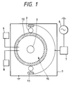
- Fig. 1 is a typical view showing the arrangement of a side cross-section of a plasma processing apparatus, in which a capacitor is arranged between a matching circuit and cathode electrodes, according to the first embodiment of the present invention.
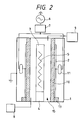
- Fig. 2 is a typical view showing the arrangement of a longitudinal cross-section of the plasma processing apparatus, in which a capacitor is arranged between a matching circuit and cathode electrodes, according to the first embodiment of the present invention.
- Fig. 3 is a typical view showing a longitudinal cross-section of a plasma processing apparatus according to a modification of the first embodiment of the present invention.
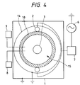
- Fig. 4 is a typical view showing the arrangement of a side cross-section of a plasma processing apparatus, having an earth shield covering a reaction vessel to remove a high-frequency wave power source line extending from a matching circuit to a cathode electrode, according to the second embodiment of the present invention.
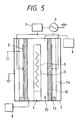
- Fig. 5 is a typical view showing the arrangement of a longitudinal cross-section of a plasma processing apparatus, having an earth shield covering a reaction vessel to remove a high-frequency wave power source line extending from a matching circuit to a cathode electrode, according to the second embodiment of the present invention.
- Fig. 6 is a typical view showing a state in which cathode electrodes shown in Fig. 4 are arranged on a concentric circle.
- Fig. 7 is a typical view showing a longitudinal cross-section of a plasma processing apparatus according to a modification of the second embodiment of the present invention.
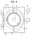
- Fig. 8 is a typical view showing the arrangement of a side cross-section of a plasma processing apparatus, having a capacitor arranged between a matching circuit and a cathode electrode and having an earth shield covering a reaction vessel to remove a high-frequency wave power source line extending from the matching circuit to the cathode electrode, according to the third embodiment of the present invention.
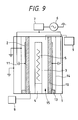
- Fig. 9 is a typical view showing the arrangement of a longitudinal cross-section of the plasma processing apparatus, having a capacitor arranged between a matching circuit and a cathode electrode and having an earth shield covering a reaction vessel to remove a high-frequency wave power source line extending from the matching circuit to the cathode electrode, according to the third embodiment of the present invention.
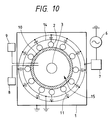
- Fig. 10 is a typical view showing a state wherein a large number of cathode electrodes shown in Fig. 7 are arranged on a concentric circle.
- Fig. 11 is a typical view showing a state wherein substrates to be processed shown in Fig. 10 are arranged on a concentric circle.
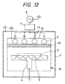
- Fig. 12 is a typical view showing a longitudinal cross-section of a plasma processing apparatus according to a modification of the third embodiment of the present invention.
- Fig. 13 is a typical view showing a cross-section of a conventional plasma processing apparatus.
- the present inventors concentratedly examined the above problems on a conventional method and apparatus.
- a plasma distribution was sensitive with respect to the shape of a cathode electrode in comparison with the plasma distribution of the conventional apparatus, and the size of a discharge apparatus was 1/10 or less the wavelength of a high-frequency wave. For this reason, influence of a stationary wave began to occur. As a result, it was found that nonuniform processing occurred.
- a high-frequency wave power output a high-frequency wave power source 7 is applied onto a cylindrical cathode electrode 102 through a matching circuit 107 and carried to cause a high-frequency wave electric field between the cathode electrode 102 and a substrate to be processed 103 opposing the cathode electrode 102 to generate a plasma, thereby performing a plasma process onto the substrate to be processed 103.
- an electrophotographic photosensitive material serving as a substrate to be process generally has a diameter of about 100 mm. For this reason, the diameter d of the cathode is about 200 mm to 300 mm.
- the transmission distance of the high-frequency wave to the opposite side of the cathode electrode along the peripheral surface is 1.57 d.
- the distance is about 390 mm.
- the frequency of the high-frequency wave is changed from 13.56 MHz (conventional frequency) to 100 MHz, a wavelength ⁇ is about 22 m to 3 m in the air. More specifically, at 100 MHz, a high-frequency wave applied from one point on the periphery of the cathode electrode transmits through the cathode electrode peripheral surface to reach the opposite side.
- an electric field distribution begins to occur on the cathode electrode periphery due to influence of a stationary wave.
- the high-frequency wave electric field also influences the cathode electrode surface, a nonuniform electric field on the inner periphery of the cathode electrode occurs, and nonuniform discharge occurs in the circumference direction.
- the length of an electrophotographic photosensitive material serving as a substrate to be processed is generally about 350 mm, so that a cathode electrode length is about 350 mm to 400 mm. For this reason, as in the peripheral direction described above, nonuniform discharge occurs also in an axial direction.
- the plasma density nonuniformity is defined as a value obtained by dividing the difference between the maximum value and minimum value of the plasma density.
- the plasma density nonuniformity was ⁇ 10% or higher at almost 30 MHz, and it was apparent that nonuniformity of a high-frequency wave voltage on the cathode electrode at the discharge frequency became conspicuous.
- the width of energy of ions incident on a substrate to be processed was measured, the width was about 30 eV at 13.56 MHz, about 15 eV at 30 MHz, and about 10 eV at 100 MHz or higher.
- a small energy width is important because controllability can be improved, and the frequency of 30 MHz or higher is preferably used. Therefore, it is very important in process that a plasma density is free from nonuniformity in this frequency range.
- the high-frequency wave power supplied from a high-frequency wave power source is adjustment in impedance to match the impedance with the impedance of the plasma, and the high-frequency wave power is applied to the rear surface of the cathode electrode.
- the high-frequency wave is transmitted from the rear surface of the cathode electrode to the surface peel of the cathode electrode to reach the front surface of the cathode electrode, so that the high-frequency wave power is supplied to the plasma.
- it is effective that the high-frequency wave distribution transmitted to the rear or front surface of the cathode is adjusted.
- a reaction vessel must not be constituted by a cathode electrode, or a cathode electrode must not be arranged in a reaction vessel. It is best that a cathode electrode is arranged outside the reaction vessel. In order to supply a high-frequency wave power from the cathode electrode outside the reaction vessel to a plasma in the reaction vessel, a portion between the cathode electrode and the plasma must consist of a dielectric material.
- any dielectric material having small loss of a high-frequency wave may be used, e.g., alumina ceramic, quartz glass, pyrex glass, teflon, or the like can be used.
- the reaction vessel When such a dielectric material is used as a part of the reaction vessel which can be reduced in pressure, the reaction vessel must have a thickness which can withstand the atmospheric pressure because the reaction vessel is reduced in pressure. Depending on the shape or size, the thickness must be generally set to at least 5 mm or more, preferably, 10 mm or more.
- a reactance component 1/j ⁇ C of a complex impedance generated by an electrostatic capacitor C of the dielectric material becomes 10 ⁇ to 50 ⁇ which is almost equal to that of the impedance of the plasma, and it is difficult to efficiently supply the high-frequency wave to the plasma.
- the discharge frequency is increased to 30 MHz to 600 MHz, a complex impedance generated by the dielectric material decreases in inverse proportion to the frequency. For this reason, even if the dielectric material having the above thickness is arranged between the cathode electrode and the plasma, the high-frequency wave can be efficiently supplied to the plasma.
- the arrangement in which the cathode electrode is arranged outside the reaction vessel is effective because a high-frequency wave can be efficiently supplied at a discharge frequency of 30 MHz or higher.
- the shape and material of the cathode electrode can be considerably changed, a complex impedance at an arbitrary point on the cathode electrode can be changed, and the above problem can be solved.
- the optimum shape and the optimum constituent material of the cathode electrode change depending on the shape of a substrate to be processed, plasma processing conditions, and a discharge frequency
- the cathode electrode when the cathode electrode is outside the reaction vessel, only the cathode electrode may be exchanged, and the reaction vessel is not temporarily opened in the air.
- the above method can easily cope with changes in various processing conditions.
- the optimum cathode electrode can be determined by try-and-error in the method considerably easier than in a conventional method.
- the above means can be easily executed because the cathode electrode is arranged outside the reaction vessel. However, when the cathode electrode can be arranged outside the reaction vessel as described above, this arrangement can also be easily applied to a parallel-plate-type plasma processing apparatus.
- a cathode electrode is arranged outside a reaction vessel, and a dielectric material serving as a buffer function is arranged between the cathode electrode and a plasma, a high-frequency stationary wave on the cathode electrode causing high-frequency wave voltage nonuniformity at a frequency of 30 MHz to 600 MHz higher than a conventional frequency is prevented from reflecting nonuniformity of the plasma strength.
- a high-frequency stationary wave on the cathode electrode causing high-frequency wave voltage nonuniformity at a frequency of 30 MHz to 600 MHz higher than a conventional frequency is prevented from reflecting nonuniformity of the plasma strength.
- the high-frequency wave power is separately applied to a plurality of cathode electrodes.
- This method is optimum in a case wherein the surface area of each cathode is decreased to prevent a stationary wave from easily occurring, and a plasma having a large area is formed.
- a high-frequency wave power is supplied from the same power source to a plurality of cathode electrodes through a matching circuit
- the distance between the matching circuit and each cathode electrode increases, and L components of the transmission paths between the matching circuit and the cathode electrodes are different from each other.
- a frequency is high, matching cannot be established. Therefore, when capacitors are interposed between the matching circuit and the cathode electrodes to change the capacitances of the respective capacitors, L components are canceled, and matching can be established between the plurality of cathode electrodes.
- the high-frequency wave power While a high-frequency wave power is transmitted from a high-frequency wave power source to the cathode electrodes through the matching circuit, the high-frequency wave power may be transmitted to the interior of the reaction vessel through the atmospheric air and part of the dielectric material. For this reason, the plasma density becomes nonuniform. As a result, a deposition disadvantageously has a film thickness nonuniformity. Therefore, when an earth shield covering a reaction vessel having a plurality of cathode electrodes arranged thereoutside except for high-frequency wave transmission paths extending from a matching circuit to the cathode electrodes is arranged, the high-frequency wave power can be prevented from being transmitted to the interior of the reaction vessel through the atmospheric air. As a result, the uniformity of the film thickness can be advantageously improved.
- Fig. 1 is a typical view showing the arrangement of a side cross-section of a plasma processing apparatus according to the first embodiment of the present invention
- Fig. 2 is a typical view showing the arrangement of the first embodiment of the present invention.
- a plasma processing apparatus comprises, as shown in Figs. 1 and 2, a cylindrical dielectric member 10 constituting the side portion of a reaction vessel 15 which can be reduced in pressure, and an earth shield 1, for preventing high-frequency wave leakage, which forms the upper and bottom portions of the reaction vessel 15 and surrounds the side portion of the reaction vessel 15.
- an earth shield 1 for preventing high-frequency wave leakage, which forms the upper and bottom portions of the reaction vessel 15 and surrounds the side portion of the reaction vessel 15.
- cathode electrodes 2 are arranged to be electrically insulated from the earth shield 1 by an insulating material 13. More specifically, the cathode electrodes 2 are arranged outside the reaction vessel 15.
- a cylindrical film-formed substrate 3 serving as a counter electrode of the cathode electrodes 2 is arranged inside the reaction vessel 15 whose side portion is constituted by the dielectric member 10.
- the film-formed substrate 3 is heated from its inside to a predetermined temperature by a heater 5 arranged in the reaction vessel 15, and is held by a substrate holder 4 having a rotating mechanism driven by a motor 12.
- the film-formed substrate 3 and the substrate holder 4 for holding the film-formed substrate 3 is grounded, and the film-formed substrate 3 is used as the counter electrode of the cathode electrodes 2.
- An evacuation means 8 for evacuating the reaction vessel 15 which is partially constituted by the dielectric member 10 and a gas supply means 9 for supplying a gas into the reaction vessel 15 are attached to the plasma processing apparatus.
- a matching circuit 7 arranged outside the earth shield 1 is connected to the cathode electrodes 2 through capacitors 11, and a high-frequency wave power source 6 is connected to the matching circuit 7.
- the capacitances of the capacitors 11 connected between the matching circuit 7 and the cathode electrodes 2 are changed to values which cancel L components of the transmission paths extending from the matching circuit 7 to the cathode electrodes 2.
- the gas supply means 9 feeds a film-forming source gas such as a silane gas, disilane gas, a methane gas, or an ethane gas and a doping gas such as a diborane gas to keep the pressure in the reaction vessel 15 in the range of several 10 mTorr to several mTorr.
- a film-forming source gas such as a silane gas, disilane gas, a methane gas, or an ethane gas and a doping gas such as a diborane gas
- the high-frequency wave power source 6 supplies a high-frequency wave power of 30 MHz to 600 MHz or less to the cathode electrodes 2 through the matching circuit 7 and the capacitor 11 to generate a plasma between the cathode electrodes 2 and the film-formed substrate 3 arranged inside the dielectric member 10, thereby decomposing the source gas.
- an a-Si film is uniformly deposited on the film-formed substrate 3 heated to about 200°C to 350°C by the heater 5.
- Fig. 3 is a typical view showing a longitudinal cross-section of a plasma processing apparatus according to a modification of the first embodiment of the present invention.
- the parallel-plate-type plasma processing apparatus shown in Fig. 3 comprises a reaction vessel 15 which has an upper portion constituted by a dielectric member 10 and can be reduced in pressure.
- the reaction vessel 15 is surrounded by the earth shield 1.
- a plurality of cathode electrodes 2 are arranged on the outside surface (surface on the atmospheric-air side) of the dielectric member 10. More specifically, the cathode electrodes 2 are arranged outside the reaction vessel 15. Inside the reaction vessel 15 whose upper portion is constituted by the dielectric member 10, a plate-like film-formed substrate 3 serving as a counter electrode of the cathode electrodes 2 is arranged.
- the film-formed substrate 3 is heated from its inside to a predetermined temperature by a heater 5 arranged in the reaction vessel 15, and is held by a substrate holder 4 having a rotating mechanism driven by a motor 12.
- the film-formed substrate 3 and the substrate holder 4 for holding the film-formed substrate 3 is grounded.
- An evacuation means 8 for evacuating the reaction vessel 15 which is partially constituted by the dielectric member 10 and a gas supply means 9 for supplying a gas into the reaction vessel 15 are attached to the plasma processing apparatus.
- a matching circuit 7 arranged outside the earth shield 1 is connected to the cathode electrodes 2 through capacitors 11, and a high-frequency wave power source 6 is connected to the matching circuit 7.
- the capacitances of the capacitors 11 connected between the matching circuit 7 and the cathode electrodes 2 are changed to values which cancel L components of the transmission paths extending from the matching circuit 7 to the cathode electrodes 2.
- Fig. 4 is a typical view showing the arrangement of a side cross-section of a plasma processing apparatus according to the second embodiment of the present invention
- Fig. 5 is a typical view showing the arrangement of a longitudinal cross-section of the second embodiment of the present invention.
- the same reference numerals as in the first embodiment shown in Figs. 1 and 2 denote the same parts in Figs. 4 and 5.
- a plasma processing apparatus comprises, as shown in Figs. 4 and 5, a cylindrical dielectric member 10 constituting the side portion of a reaction vessel 15 which can be reduced in pressure, and a first earth shield 1, for preventing high-frequency wave leakage, which forms the upper and bottom portions of the reaction vessel 15 and surrounds the side portion of the reaction vessel 15.
- a cylindrical dielectric member 10 constituting the side portion of a reaction vessel 15 which can be reduced in pressure
- a first earth shield 1 for preventing high-frequency wave leakage, which forms the upper and bottom portions of the reaction vessel 15 and surrounds the side portion of the reaction vessel 15.
- cathode electrodes 2 are arranged to be electrically insulated from the first earth shield 1 by an insulating material 13. More specifically, the cathode electrodes 2 are arranged outside the reaction vessel 15.
- a cylindrical film-formed substrate 3 serving as a counter electrode of the cathode electrodes 2 is arranged inside the reaction vessel 15 whose side portion is constituted by the dielectric member 10.
- the film-formed substrate 3 is heated from its inside to a predetermined temperature by a heater 5 arranged in the reaction vessel 15, and is held by a substrate holder 4 having a rotating mechanism driven by a motor 12.
- the substrate holder 4 for holding the film-formed substrate 3 is grounded, and the film-formed substrate 3 is used as the counter electrode of the cathode electrodes 2.
- An evacuation means 8 for evacuating the reaction vessel 15 which is partially constituted by the dielectric member 10 and a gas supply means 9 for supplying a gas into the reaction vessel 15 are attached to the plasma processing apparatus.
- a matching circuit 7 arranged outside the first earth shield 1 is connected to the cathode electrodes 2, and a high-frequency wave power source 6 is connected to the matching circuit 7.
- a second earth shield 14 covering the reaction vessel 15 having the plurality of cathode electrodes 2 arranged thereoutside except for high-frequency wave transmission paths extending from the matching circuit 7 to the cathode electrodes 2 is arranged.
- a plurality of openings (not shown) for connecting the high-frequency wave transmission paths from the outside of the second earth shield 14 to the cathode electrodes 2 are formed in the second earth shield 14.
- the reaction vessel having a plurality of cathode electrodes arranged thereoutside is covered with the earth shields outside the high-frequency wave transmission paths extending from the matching circuit to the cathode electrodes, so that the high-frequency wave power can be prevented from being transmitted to the interior of the reaction vessel through the atmospheric air.
- the substrates to be processed are cylindrical each, and the substrates to be processed and the reaction vessel are arranged on a concentric circle, very uniform deposition films can be formed on a plurality of substrates to be processed at a high speed.
- the number of cathode electrodes is not limited to two, and, as shown in Fig. 6, a plurality of cathode electrodes are preferably arranged to prevent a high-frequency stationary wave from easily occurring and to make the plasma distribution more uniform.
- the present invention is not limited to the cylindrical coaxial-type plasma processing apparatus and method, and the present is also preferable for a parallel-plate-type plasma processing apparatus and method.
- FIG. 7 is a typical view showing a longitudinal cross-section of a plasma processing apparatus according to a modification of the second embodiment of the present invention.
- the same reference numerals as in the first embodiment shown in Figs. 1 and 2 denote the same parts in Fig. 7.
- a parallel-plate-type plasma processing apparatus as shown in Fig. 7 comprises a reaction vessel 15 whose upper portion is constituted by a dielectric member 10 and which can be reduced in pressure.
- the reaction vessel 15 is surrounded by an earth shield 1.
- a plurality of cathode electrodes 2 are arranged on the outside surface (surface on the atmospheric-air side) of the dielectric member 10. More specifically, the cathode electrodes 2 are arranged outside the reaction vessel 15.
- a plate-like film-formed substrate 3 serving as a counter electrode of the cathode electrodes 2 is arranged inside the reaction vessel 15 whose upper portion is constituted by the dielectric member 10.
- the film-formed substrate 3 is heated from its inside to a predetermined temperature by a heater 5 arranged in the reaction vessel 15, and is held by a substrate holder 4 having a rotating mechanism driven by a motor 12.
- the film-formed substrate 3 and the substrate holder 4 for holding the film-formed substrate 3 is grounded, and the film-formed substrate 3 is used as the counter electrode of the cathode electrodes 2.
- An evacuation means (not shown) for evacuating the reaction vessel 15 which is partially constituted by the dielectric member 10 and a gas supply means (not shown) for supplying a gas into the reaction vessel 15 are attached to the plasma processing apparatus.
- a matching circuit 7 arranged outside the first earth shield 1 is connected to the cathode electrodes 2, and a high-frequency wave power source 6 is connected to the matching circuit 7.
- a second earth shield 14 covering the reaction vessel 15 having the plurality of cathode electrodes 2 arranged thereoutside except for high-frequency wave transmission paths extending from the matching circuit 7 to the cathode electrodes 2 is arranged.
- a plurality of openings (not shown) for connecting the high-frequency wave transmission paths from the outside of the second earth shield 14 to the cathode electrodes 2 are formed in the second earth shield 14.
- Fig. 8 is a typical view showing the arrangement of a side cross-section of a plasma processing apparatus according to the third embodiment of the present invention
- Fig. 9 is a typical view showing the arrangement of a longitudinal cross-section of the third embodiment of the present invention.
- the same reference numerals as in the first and second embodiment shown in Figs. 1 to 7 denote the same parts in Figs. 8 and 9.
- a plasma processing apparatus comprises, as shown in Figs. 8 and 9, a cylindrical dielectric member 10 constituting the side portion of a reaction vessel 15 which can be reduced in pressure, and a first earth shield 1, for preventing high-frequency wave leakage, which forms the upper and bottom portions of the reaction vessel 15 and surrounds the side portion of the reaction vessel 15.
- a cylindrical dielectric member 10 constituting the side portion of a reaction vessel 15 which can be reduced in pressure
- a first earth shield 1 for preventing high-frequency wave leakage, which forms the upper and bottom portions of the reaction vessel 15 and surrounds the side portion of the reaction vessel 15.
- cathode electrodes 2 are arranged to be electrically insulated from the first earth shield 1 by an insulating material 13. More specifically, the cathode electrodes 2 are arranged outside the reaction vessel 15.
- a cylindrical film-formed substrate 3 serving as a counter electrode of the cathode electrodes 2 is arranged inside the reaction vessel 15 whose side portion is constituted by the dielectric member 10.
- the film-formed substrate 3 is heated from its inside to a predetermined temperature by a heater 5 arranged in the reaction vessel 15, and is held by a substrate holder 4 having a rotating mechanism driven by a motor 12.
- the substrate holder 4 for holding the film-formed substrate 3 is grounded, and the film-formed substrate 3 is used as the counter electrode of the cathode electrodes 2.
- a matching circuit 7 arranged outside the first earth shield 1 is connected to the cathode electrodes 2 through capacitors, and a high-frequency wave power source 6 is connected to the matching circuit 7.
- An evacuation means 8 for evacuating the reaction vessel 15 which is partially constituted by the dielectric member 10 and a gas supply means 9 for supplying a gas into the reaction vessel 15 are attached to the plasma processing apparatus.
- the capacitances of the capacitors 11 connected between the matching circuit 7 and the cathode electrodes 2 are changed to values which cancel L components of the transmission paths extending from the matching circuit 7 to the cathode electrodes 2.
- a second earth shield 14 covering the reaction vessel 15 having the plurality of cathode electrodes 2 arranged thereoutside except for high-frequency wave transmission paths extending from the matching circuit 7 to the cathode electrodes 2 is arranged.
- a plurality of openings (not shown) for connecting the high-frequency wave transmission paths from the outside of the second earth shield 14 to the cathode electrodes 2 are formed in the second earth shield 14.
- the reaction vessel having a plurality of cathode electrodes arranged thereoutside is covered with the earth shields outside the high-frequency wave transmission paths extending from the matching circuit to the cathode electrodes, so that the high-frequency wave power can be prevented from being transmitted to the interior of the reaction vessel through the atmospheric air.
- the substrates to be processed are cylindrical each, and the substrates to be processed and the reaction vessel are arranged on a concentric circle, very uniform deposition films can be formed on the plurality of substrates to be processed at a high speed.
- the number of cathode electrodes is not limited to two, and, as shown in Fig. 10, a plurality of cathode electrodes are preferably arranged to prevent a high-frequency stationary wave from easily occurring and to make the plasma distribution more uniform. Even if the plurality of film-formed substrates 3 are arranged on a concentric circle as shown in Fig. 11, a nonuniform film is rarely formed.
- FIG. 12 is a typical view showing a longitudinal cross-section of a plasma processing apparatus according to a modification of the third embodiment of the present invention.
- the same reference numerals as in the first and second embodiments shown in Figs. 1 to 7 denote the same parts in Fig. 12.
- a parallel-plate-type plasma processing apparatus as shown in Fig. 12 comprises a reaction vessel 15 whose upper portion is constituted by a dielectric member 10 and which can be reduced in pressure.
- the reaction vessel 15 is surrounded by an earth shield 1.
- a plurality of cathode electrodes 2 are arranged on the outside surface (surface on the atmospheric-air side) of the dielectric member 10. More specifically, the cathode electrodes 2 are arranged outside the reaction vessel 15.
- a plate-like film-formed substrate 3 serving as a counter electrode of the cathode electrodes 2 is arranged inside the reaction vessel 15 whose upper portion is constituted by the dielectric member 10.
- the film-formed substrate 3 is heated from its inside to a predetermined temperature by a heater 5 arranged in the reaction vessel 15, and is held by a substrate holder 4 having a rotating mechanism driven by a motor 12.
- the substrate holder 4 for holding the film-formed substrate 3 is grounded, and the film-formed substrate 3 is used as the counter electrode of the cathode electrodes 2.
- An evacuation means (not shown) for evacuating the reaction vessel 15 which is partially constituted by the dielectric member 10 and a gas supply means (not shown) for supplying a gas into the reaction vessel 15 are attached to the plasma processing apparatus.
- a matching circuit 7 arranged outside the first earth shield 1 is connected to the cathode electrodes 2 through capacitors 11, and a high-frequency wave power source 6 is connected to the matching circuit 7.
- the capacitances of the capacitors 11 connected between the matching circuit 7 and the cathode electrodes 2 are changed to values which cancel L components of the transmission paths extending from the matching circuit 7 to the cathode electrodes 2.
- a second earth shield 14 covering the reaction vessel 15 having the plurality of cathode electrodes 2 arranged thereoutside except for high-frequency wave transmission paths extending from the matching circuit 7 to the cathode electrodes 2 is arranged.
- a plurality of openings (not shown) for connecting the high-frequency wave transmission paths from the outside of the second earth shield 14 to the cathode electrodes 2 are formed in the second earth shield 14.
- a cathode electrode As a cathode electrode, a simply circular Al cathode electrode having an inner diameter of 250 mm and a length of 300 mm was used. The cathode electrode was arranged outside an alumina-ceramic dielectric tube which partially constituted a reaction vessel and had a thickness of 10 mm.
- a film thickness nonuniformity obtained when film formation was performed by using the externally arranged cathode electrodes was performed by using the externally arranged cathode electrodes.
- a comparison experiment for a film thickness nonuniformity obtained in a case wherein simply cylindrical Al cathode electrodes having an inner diameter of 250 mm and a length of 300 mm was arranged in a reaction vessel was performed.
- the film thickness nonuniformities were about ⁇ 15% in use of the externally arranged cathode electrodes and about ⁇ 30% in use of the simply circular cathode.
- An effect of improving a film thickness distribution obtained by using the externally arranged cathode electrodes could be confirmed.
- the respective films were considerably influenced by only a plasma distribution.
- the a-Si film could be sufficiently in practical use, e.g., in an electrophotographic photosensitive device, an image input line sensor, or the like.
- the high-frequency wave power source 6 having a frequency of 105 MHz was used, and a discharge experiment was performed under the conditions shown in Table 1 of Example 1.
- a reactance L between a matching circuit and a load was set to 404.5 nH, and a high-power capacitor was arranged as shown in Fig. 1.
- the obtained results are shown in Table 2.
- a rectangular substrate to be processed was used. Capacitors were interposed between a matching circuit and cathode electrodes, and the cathode electrodes were arranged outside an alumina-ceramic dielectric rectangular member which partially constituted a reaction vessel and had a thickness of 20 mm. For comparison, a film thickness nonuniformity obtained when cathode electrodes were arranged inside a reaction vessel to perform film formation under the conditions shown in Table 3 was measured. When the cathode electrodes were arranged outside the reaction vessel, and the capacitors were interposed, a film thickness nonuniformity was about ⁇ 18%; when the cathode electrodes were arranged inside the reaction vessel, a film thickness nonuniformity was about ⁇ 35%.
- the respective films were considerably influenced by only a plasma distribution.
- the a-Si film could be sufficiently in practical use, e.g., in an electrophotographic photosensitive device, an image input line sensor, or the like.
- a film thickness nonuniformity obtained when a film forming apparatus having the second earth shield was measured. As a result, the film thickness nonuniformity was about ⁇ 11%. When the second earth shield was not used, the film thickness nonuniformity was about ⁇ 15%. It was confirmed that an effect of improving a film thickness distribution was obtained by using the second earth shield.
- the respective films were considerably influenced by only a plasma distribution.
- the a-Si film could be sufficiently in practical use, e.g., in an electrophotographic photosensitive device, an image input line sensor, or the like.
- the second earth shield covering a reaction vessel having the plurality of cathode electrodes arranged thereoutside except for high-frequency wave transmission paths extending from the matching circuit to the cathode electrodes, a complex impedance at a high frequency can be increased.
- the arrangement is designed such that only a portion of the high-frequency path free from the earth shield can be controlled, a problem of film thickness nonuniformity caused by a high discharge frequency can be solved.
- a film thickness nonuniformity was measured by using an apparatus in which the second earth shield was arranged. As a result, the film thickness nonuniformity was about ⁇ 13% in comparison with about ⁇ 18% obtained by using a simple plate, and preferable film thickness uniformity was exhibited.
- the respective films were considerably influenced by only a plasma distribution.
- the a-Si film could be sufficiently in practical use, e.g., in an electrophotographic photosensitive device, an image input line sensor, or the like.
- cathode electrodes simply cylindrical Al cathode electrodes each having an inner diameter of 250 mm and a length of 300 mm was used.
- the cathode electrodes were arranged outside an alumina-ceramic dielectric tube which partially constituted a reaction vessel and had a thickness of 10 mm.
- a second earth shield covering the reaction vessel having the plurality of cathode electrodes arranged thereoutside except for high-frequency wave transmission paths extending from the matching circuit to the cathode electrodes was arranged.
- the cathode length was not limited to the value in this example.
- a film thickness nonuniformity obtained when film formation was performed by using the externally arranged cathode electrode was performed by using the externally arranged cathode electrode.
- comparison experiments for film thickness nonuniformities obtained in a case wherein simply cylindrical Al cathode electrodes each having a length of 300 mm was arranged in a reaction vessel was performed; a case wherein externally arranged cathodes shown in Fig. 1 were used, and capacitors were interposed between a matching circuit and the cathodes; and a case wherein a second earth shield covering the reaction vessel having the plurality of cathode electrodes arranged thereoutside except for high-frequency wave transmission paths extending from the matching circuit to the cathode electrodes was arranged was made.
- the film thickness nonuniformity was about ⁇ 15% when cylindrical cathode electrodes was arranged in a reaction vessel; ⁇ 13% when the capacitors were interposed; ⁇ 11% when the second earth shield was interposed; and ⁇ 9% when the apparatus using the capacitors and the second earth shield was used. An effect of improving a film thickness distribution could be confirmed.
- the respective films were considerably influenced by only a plasma distribution.
- the a-Si film could be sufficiently in practical use, e.g., in- an electrophotographic photosensitive device, an image input line sensor, or the like.
- the capacitors are arranged to the cathode electrodes, the second earth shield covering the reaction vessel having the plurality of cathode electrodes arranged thereoutside except for high-frequency wave transmission paths extending from the matching circuit to the cathode electrodes, and a high-frequency wave is supplied to a plasma through the dielectric member partially constituting the reaction chamber which can be reduced in pressure.
- matching can be established, and loss caused by transmission of the high-frequency wave power through the atmospheric air before the high-frequency wave power reaches the cathode electrodes is maximally prevented, so that the plasma is stable.
- a problem of film thickness nonuniformity can be solved.
- cathode electrodes arranged on a concentric circle, and capacitors arranged to the respective cathode electrodes could obtain a high film formation rate of 5 nm/s.
- a parallel-plate-type plasma CVD apparatus having a second earth shield covering a reaction vessel having a plurality of cathode electrodes arranged thereoutside except for high-frequency wave transmission paths extending from a matching circuit to the cathode electrodes and capacitors interposed between a matching circuit and the cathode electrodes, an a-Si film was formed on the film-formed substrate at a discharge frequency of 100 MHz under the film-formation conditions shown in Table 3, and a film thickness nonuniformity was measured.
- the film thickness nonuniformity was about ⁇ 10%, in comparison with about ⁇ 18% obtained by using a simple plate, and preferable film thickness uniformity was exhibited.
- the respective films were considerably influenced by only a plasma distribution.
- the a-Si film could be sufficiently in practical use, e.g., in an electrophotographic photosensitive device, an image input line sensor, or the like.
- Example 7 by using the same apparatus as in Example 7, under the same conditions as in Example 7, a glass substrate was arranged on an Al cylindrical substrate surface in an axial direction, an a-Si film was formed.
- a Cr comb-shaped electrode having a cap of 250 pm for evaluating film quality (electric characteristics) was deposited on the glass substrate subjected to film formation.
- the electric characteristics of this a-Si film were evaluated by measuring a photosensitivity (photoconductivity ⁇ p/dark-conductivity ad).
- the obtained results are shown in Table 4.
- the photoconductivity ⁇ p is evaluated by a conductivity in irradiation of an He-Ne laser (wavelength: 632.8 nm) having a strength of 1 mW/cm 2 .
- ⁇ photoconductivity is 10 4 or more, and preferable film characteristics can be obtained.
- ⁇ photoconductivity is 10 3 or more, and film characteristics is free from a problem in practice.
- ⁇ photoconductivity is 10 3 or less, and film characteristics is slightly preferable in practice.
- An a-Si film formed in this example had film quality higher than that of an a-Si film formed by a conventional apparatus and nonuniformity less than that of the a-Si film formed by the conventional apparatus.
- the a-Si film formed in this example could be sufficiently in practical use, e.g., in an electrophotographic photosensitive device, an image input line sensor, or the like.
- a high-frequency wave power having 30 MHz or higher and 600 MHz or lower is supplied to the cathode electrodes through a matching circuit to generate a plasma between the cathode electrodes and the counter electrode, and a plasma process is performed to a substrate to be processed arranged on the counter electrode, the plurality of cathode electrodes are arranged outside the reaction vessel, and the reaction vessel between the cathode electrodes and the counter electrode is partially constituted by a dielectric member, so that homogeneous high-frequency wave discharge having a large area can be easily achieved, and a plasma process for a large substrate can be uniformly performed at a high speed.
- the dielectric material buffers the non-uniformity of the high-frequency wave voltage on the cathode electrodes to make the plasma distribution uniform. For this reason, a uniform plasma process can be performed to a substrate to be processed.
- the cathode electrodes are arranged outside the reaction vessel, the degree of freedom of the design of the cathode electrodes increases, the optimum shape and optimum constituent material of the cathode electrode can be easily determined.
- a high-frequency wave power is separately supplied to a plurality of cathode electrodes, a high-frequency stationary wave can be prevented from easily occurring by decreasing a surface area per cathode, and the arrangement is optimum to form a large-area plasma.
- the transmission paths between the matching circuit and the cathode electrodes are different from each other in length, and reactances L of the transmission paths are different from each other. For this reason, matching may not be established at a high frequency.
- capacitors are arranged on the high-frequency wave transmission paths between the matching circuit and the cathode electrodes, the L components can be canceled, and the matching can be reliably established.
- the apparatus has an earth shield covering a reaction vessel having the cathode electrodes arranged thereoutside except for high-frequency wave transmission paths extending from the matching circuit to the cathode electrodes, the high-frequency wave power is prevented from being transmitted to the interior of the reaction vessel through the matching circuit and the atmospheric air in the middle of the high-frequency wave transmission paths. For this reason, the plasma distribution can be prevented from being nonuniform.
Abstract
Description
- The present invention relates to a plasma processing apparatus and a processing method and, more particularly, to a plasma processing apparatus and a processing method such as: a plasma CVD apparatus and a film forming method in which a crystalline or non-monocrystalline functional deposition film effective for an electrophotographic photosensitive device serving as a semiconductor device, an image input line sensor, an image-pickup device, or a photomotive device; a sputtering apparatus and a film forming method which can preferably form a semiconductor device, an insulating film serving as an optical element, or a metal wire; or an etching apparatus and method for a semiconductor device.
- As a plasma process used in a semiconductor or the like, various methods are used depending on applications. For example, an apparatus and a method variably using the characteristics of a plasma, such as film formation for an oxide film, a nitride film, and an amorphous-silicon-based semiconductor film using a plasma CVD method, film formation for a metal wiring film or the like using a sputtering method, or a micropatterning technique or the like using etching. In addition, in recent years, a demand for improvement of film quality and processing performance becomes strong, and various devices are examined. In particular, since a plasma process using a high-frequency power has stable discharging and can be applied to an insulating material of an oxide film or a nitride film, the plasma process is widely applied.
- Conventionally, the oscillation frequency of a discharging high-frequency wave power source used in a plasma process such as plasma CVD is generally 13.56 MHz. A plasma CVD apparatus generally used in deposition film formation is shown in Fig. 13. Fig. 13 shows a film formation apparatus for a cylindrical amorphous-silicon film (to be referred to as an a-Si film hereinafter) for a cylindrical electrophotographic photosensitive material. A film forming method for an a-Si film will be described below with reference to Fig. 13.
- The film formation apparatus shown in Fig. 13 is constituted such that, in a reaction vessel 101 which can be reduced in pressure, a
cylindrical cathode electrode 102 electrically insulated from the reaction vessel 101 and a cylindrical film-formedsubstrate 103 serving as a counter electrode are arranged by aninsulating material 113. The film-formedsubstrate 103 is heated therefrom to a predetermined temperature by aheater 105 arranged in the film-formedsubstrate 103, and is held on asubstrate holder 104 having a rotating mechanism driven by amotor 112. A high-frequencywave power source 106 is connected to thecathode electrode 102 through amatching circuit 107. An evacuating means 108 for evacuating the reaction vessel 101 and a gas supply means 109 for supplying a gas into the reaction vessel 101 are attached to the film formation apparatus. - In order to form an a-Si film by the above apparatus, the reaction vessel 101 is evacuated by the evacuating
means 108 to a high degree of vacuum, and the gas supply means 109 feeds a source gas such as a silane gas, disilane gas, a methane gas, or an ethane gas or a doping gas such as a diborane gas to keep the pressure in the reaction vessel 101 in the range of several 10 mTorr to several mTorr. The high-frequencywave power source 106 supplies a high-frequency wave power of 13.56 MHz to thecathode electrode 102 to generate a plasma between thecathode electrode 102 and the film-formedsubstrate 103, thereby decomposing the source gas. At this time, an a-Si film is deposited on the film-formedsubstrate 103 heated to about 200°C to 350°C by theheater 105. - A deposition rate for obtaining an a-Si film which satisfies the performance of an electrophotographic photosensitive material by the film forming method described above is the maximum of about 6 pm/hour. When the deposition rate is higher than 6 µm/hour, the characteristic feature of the photosensitive material cannot be obtained. When the a-Si film is generally used as an electrophotographic photosensitive material, the a-Si film requires a thickness of at least 20 pm to 30 pm to obtain charging performance, and a long period of time is required to manufacture an electrophotographic photosensitive material.
- In recent years, the report (Plasma Chemistry and Plasma Processing,
Vol 7, No. 3, (1987) p.267 - p.273) of a plasma CVD method using a parallel-plate-type plasma CVD apparatus and a high-frequency wave power source of 13.56 MHz or higher is made. This report shows the probability that a deposition rate can be increased without degrading the performance of a deposition film by making a discharge frequency higher than the conventional frequency of 13.56 MHz. The report attracts attention. An attempt to increasing the discharge frequency has been widely examined in sputtering or the like. - The present inventors made an examination by using the conventional plasma CVD method and apparatus described above and using a high-frequency wave power having a frequency higher than a conventional discharge frequency of 13.56 MHz to increase a deposition rate of a high-quality film.
- As a result, when the frequency was increased, as an object, a high-quality film could be manufactured at a deposition rate higher than a conventional deposition rate. However, when the discharge frequency of 13.56 MHz was used, the following problem is newly posed. More specifically, when the discharge frequency was increased, a plasma is eccentrically located to make the deposition rate nonuniform. As a result, in a substrate to be processed such as an electrophotographic photosensitive material having a relatively large area, a film thickness nonuniformity (for example, a film thickness nonuniformity of ±20% or more in an electrophotographic photosensitive material) is generated.
- Such a film thickness nonuniformity poses a serious problem when not only an electrophotographic photosensitive material but also a crystalline or non-monocrystalline functional deposition film used an image input line sensor, an image-pickup device, a photomotive device, or the like is formed. In another plasma process such as dry etching or sputtering, when a discharge frequency is increased, similarly, nonuniform processing occurs. For this reason, the high-frequency wave power having a frequency higher than 13.56 MHz cannot be practically used without any problem.
- It is an object of the present invention to overcome the above conventional problem and to provide a method and apparatus capable of uniformly performing a plasma process such as CVD, sputtering, etching, or ashing to a substrate having a relatively large area at a process rate which cannot be achieved by a conventional plasma process.
- In particular, there is provided a deposition film forming method using plasma CVD which can form a deposition film having an extremely uniform thickness at a high speed, and can efficiently form a semiconductor device.
- In order to achieve the above object, according to the present invention, there is provided a plasma processing apparatus in which a counter electrode opposing a cathode electrode is arranged in a reaction vessel which can be reduced in pressure, a high-frequency wave power is applied to the cathode electrode through a matching circuit to generate a plasma between the cathode electrode and the counter electrode, and a plasma process is performed to a substrate to be processed arranged on the counter electrode, characterized in that a plurality of cathode electrodes are arranged outside the reaction vessel, and the reaction vessel arranged between the cathode electrodes and the counter electrode partially consists of a dielectric material.
- In the plasma processing apparatus, capacitors are preferably arranged on high-frequency wave transmission paths between the matching circuit and the cathode electrodes, or/and an earth shield covering the reaction vessel arranged outside the cathode electrodes except for the high-frequency wave transmission paths between the matching circuit and the cathode electrodes is preferably arranged. The above apparatus is especially preferable when the high-frequency wave power is 30 MHz to 600 MHz or less.
- The plasma processing apparatus is preferable in a case wherein a reaction vessel is cylindrical, and the plurality of cathode electrodes are arranged at equal intervals outside the cylindrical reaction vessel; a case wherein the reaction vessel is cylindrical, and the substrate to be processed and the reaction vessel are arranged on a concentric circle; in a case wherein the plurality of substrates to be processed are arranged on a concentric circle; or in a case wherein the substrate to be processed is flat, and the subject to be processed opposes the plurality of cathode electrodes.
- In addition, a plasma processing method for performing a plasma process to a substrate to be processed by using the above plasma processing apparatus belongs to the present invention.
- Fig. 1 is a typical view showing the arrangement of a side cross-section of a plasma processing apparatus, in which a capacitor is arranged between a matching circuit and cathode electrodes, according to the first embodiment of the present invention.
- Fig. 2 is a typical view showing the arrangement of a longitudinal cross-section of the plasma processing apparatus, in which a capacitor is arranged between a matching circuit and cathode electrodes, according to the first embodiment of the present invention.
- Fig. 3 is a typical view showing a longitudinal cross-section of a plasma processing apparatus according to a modification of the first embodiment of the present invention.
- Fig. 4 is a typical view showing the arrangement of a side cross-section of a plasma processing apparatus, having an earth shield covering a reaction vessel to remove a high-frequency wave power source line extending from a matching circuit to a cathode electrode, according to the second embodiment of the present invention.
- Fig. 5 is a typical view showing the arrangement of a longitudinal cross-section of a plasma processing apparatus, having an earth shield covering a reaction vessel to remove a high-frequency wave power source line extending from a matching circuit to a cathode electrode, according to the second embodiment of the present invention.
- Fig. 6 is a typical view showing a state in which cathode electrodes shown in Fig. 4 are arranged on a concentric circle.
- Fig. 7 is a typical view showing a longitudinal cross-section of a plasma processing apparatus according to a modification of the second embodiment of the present invention.
- Fig. 8 is a typical view showing the arrangement of a side cross-section of a plasma processing apparatus, having a capacitor arranged between a matching circuit and a cathode electrode and having an earth shield covering a reaction vessel to remove a high-frequency wave power source line extending from the matching circuit to the cathode electrode, according to the third embodiment of the present invention.
- Fig. 9 is a typical view showing the arrangement of a longitudinal cross-section of the plasma processing apparatus, having a capacitor arranged between a matching circuit and a cathode electrode and having an earth shield covering a reaction vessel to remove a high-frequency wave power source line extending from the matching circuit to the cathode electrode, according to the third embodiment of the present invention.
- Fig. 10 is a typical view showing a state wherein a large number of cathode electrodes shown in Fig. 7 are arranged on a concentric circle.
- Fig. 11 is a typical view showing a state wherein substrates to be processed shown in Fig. 10 are arranged on a concentric circle.
- Fig. 12 is a typical view showing a longitudinal cross-section of a plasma processing apparatus according to a modification of the third embodiment of the present invention.
- Fig. 13 is a typical view showing a cross-section of a conventional plasma processing apparatus.
- The present inventors concentratedly examined the above problems on a conventional method and apparatus. As a result, at a discharge frequency higher than a conventional discharge frequency, a plasma distribution was sensitive with respect to the shape of a cathode electrode in comparison with the plasma distribution of the conventional apparatus, and the size of a discharge apparatus was 1/10 or less the wavelength of a high-frequency wave. For this reason, influence of a stationary wave began to occur. As a result, it was found that nonuniform processing occurred.
- An experiment performed to solve the above problem and achieve uniformity of a plasma and uniformity of a plasma process based on the plasma, and knowledge obtained by the experiment will be described below.
- By using an apparatus shown in Fig. 13, a high-frequency wave power output a high-frequency
wave power source 7 is applied onto acylindrical cathode electrode 102 through amatching circuit 107 and carried to cause a high-frequency wave electric field between thecathode electrode 102 and a substrate to be processed 103 opposing thecathode electrode 102 to generate a plasma, thereby performing a plasma process onto the substrate to be processed 103. In this case, an electrophotographic photosensitive material serving as a substrate to be process generally has a diameter of about 100 mm. For this reason, the diameter d of the cathode is about 200 mm to 300 mm. When a high-frequency wave is applied from one point of the periphery of the cathode electrode, the transmission distance of the high-frequency wave to the opposite side of the cathode electrode along the peripheral surface is 1.57 d. For example, when d = 250 mm, the distance is about 390 mm. When the frequency of the high-frequency wave is changed from 13.56 MHz (conventional frequency) to 100 MHz, a wavelength λ is about 22 m to 3 m in the air. More specifically, at 100 MHz, a high-frequency wave applied from one point on the periphery of the cathode electrode transmits through the cathode electrode peripheral surface to reach the opposite side. When the transmission distance along the peripheral surface is λ/10 or more, an electric field distribution begins to occur on the cathode electrode periphery due to influence of a stationary wave. The high-frequency wave electric field also influences the cathode electrode surface, a nonuniform electric field on the inner periphery of the cathode electrode occurs, and nonuniform discharge occurs in the circumference direction. - Similarly, the length of an electrophotographic photosensitive material serving as a substrate to be processed is generally about 350 mm, so that a cathode electrode length is about 350 mm to 400 mm. For this reason, as in the peripheral direction described above, nonuniform discharge occurs also in an axial direction.
- As described above, it was found that, although any problem was not posed at 13.56 MHz or a discharge frequency near 13.56 MHz, nonuniform discharge became conspicuous when the discharge frequency was made higher.
- In order to measure a frequency at which these problems are influenced and made conspicuous, discharging was performed at 13.5 MHz to 600 MHz by using the plasma CVD apparatus shown in Fig. 13 to measure plasma density nonuniformity. The plasma density nonuniformity is defined as a value obtained by dividing the difference between the maximum value and minimum value of the plasma density. As a result, the plasma density nonuniformity was ±10% or higher at almost 30 MHz, and it was apparent that nonuniformity of a high-frequency wave voltage on the cathode electrode at the discharge frequency became conspicuous.
- When the discharge frequency exceeded 600 MHz, a high-frequency wave matching circuit could not be easily designed, and transmission loss became large. It was understood that the frequency higher than 600 MHz could not be practical.
- When the width of energy of ions incident on a substrate to be processed was measured, the width was about 30 eV at 13.56 MHz, about 15 eV at 30 MHz, and about 10 eV at 100 MHz or higher. In the process using incident ion energy for the substrate to be processed, a small energy width is important because controllability can be improved, and the frequency of 30 MHz or higher is preferably used. Therefore, it is very important in process that a plasma density is free from nonuniformity in this frequency range.
- As a means for solving nonuniformity caused by nonuniform high-frequency wave voltage on the cathode electrode at 30 MHz to 600 MHz, the present inventors obtained the following knowledge.
- In order to prevent a high-frequency stationary wave causing high-frequency wave voltage nonuniformity on the cathode electrode from reflecting nonuniformity of plasma strength, the followings are required:
- a) to prevent a stationary wave from being generated on the cathode electrode surface
- b) to arrange a buffer function between a stationary wave on the cathode electrode surface and a plasma.
- In the apparatus in Fig. 13, in order to supply a high-frequency wave power to a plasma, the high-frequency wave power supplied from a high-frequency wave power source is adjustment in impedance to match the impedance with the impedance of the plasma, and the high-frequency wave power is applied to the rear surface of the cathode electrode. In addition, the high-frequency wave is transmitted from the rear surface of the cathode electrode to the surface peel of the cathode electrode to reach the front surface of the cathode electrode, so that the high-frequency wave power is supplied to the plasma. Here, in order to prevent the high-frequency wave power from being nonuniform on the cathode electrode surface, it is effective that the high-frequency wave distribution transmitted to the rear or front surface of the cathode is adjusted.
- In order to adjust the high-frequency wave distribution on the cathode electrode in the above-mentioned manner at a frequency 30 MHz to 600 MHz higher than a conventional frequency, it is important that the complex impedance of the cathode electrode can be adjusted in shape, material, and the like. For this purpose, a reaction vessel must not be constituted by a cathode electrode, or a cathode electrode must not be arranged in a reaction vessel. It is best that a cathode electrode is arranged outside the reaction vessel. In order to supply a high-frequency wave power from the cathode electrode outside the reaction vessel to a plasma in the reaction vessel, a portion between the cathode electrode and the plasma must consist of a dielectric material. In this case, any dielectric material having small loss of a high-frequency wave may be used, e.g., alumina ceramic, quartz glass, pyrex glass, teflon, or the like can be used. When such a dielectric material is used as a part of the reaction vessel which can be reduced in pressure, the reaction vessel must have a thickness which can withstand the atmospheric pressure because the reaction vessel is reduced in pressure. Depending on the shape or size, the thickness must be generally set to at least 5 mm or more, preferably, 10 mm or more. When the conventional frequency of 13.56 MHz is used, and a dielectric material having the above thickness is arranged between the cathode electrode and a plasma, a
reactance component 1/jωC of a complex impedance generated by an electrostatic capacitor C of the dielectric material becomes 10 Ω to 50 Ω which is almost equal to that of the impedance of the plasma, and it is difficult to efficiently supply the high-frequency wave to the plasma. However, when the discharge frequency is increased to 30 MHz to 600 MHz, a complex impedance generated by the dielectric material decreases in inverse proportion to the frequency. For this reason, even if the dielectric material having the above thickness is arranged between the cathode electrode and the plasma, the high-frequency wave can be efficiently supplied to the plasma. As described above, in order to obtain large-area uniform discharge which is posed as a problem at a discharge frequency of 30 MHz or higher, the arrangement in which the cathode electrode is arranged outside the reaction vessel is effective because a high-frequency wave can be efficiently supplied at a discharge frequency of 30 MHz or higher. In this manner, the shape and material of the cathode electrode can be considerably changed, a complex impedance at an arbitrary point on the cathode electrode can be changed, and the above problem can be solved. Although the optimum shape and the optimum constituent material of the cathode electrode change depending on the shape of a substrate to be processed, plasma processing conditions, and a discharge frequency, when the cathode electrode is outside the reaction vessel, only the cathode electrode may be exchanged, and the reaction vessel is not temporarily opened in the air. For this reason, the above method can easily cope with changes in various processing conditions. For the same reason, as described above, the optimum cathode electrode can be determined by try-and-error in the method considerably easier than in a conventional method. - Even if a potential distribution is left on the cathode electrode to some extent in the above method, since a dielectric material is arranged between the cathode electrode and a plasma, an effect that the uniformity of the plasma is better than that of the potential distribution on the cathode electrode can be obtained by the buffer function of the dielectric material.
- The above means can be easily executed because the cathode electrode is arranged outside the reaction vessel. However, when the cathode electrode can be arranged outside the reaction vessel as described above, this arrangement can also be easily applied to a parallel-plate-type plasma processing apparatus.
- As described above, according to the present invention, a cathode electrode is arranged outside a reaction vessel, and a dielectric material serving as a buffer function is arranged between the cathode electrode and a plasma, a high-frequency stationary wave on the cathode electrode causing high-frequency wave voltage nonuniformity at a frequency of 30 MHz to 600 MHz higher than a conventional frequency is prevented from reflecting nonuniformity of the plasma strength. In addition, in order to eliminate the influence of the stationary wave, it is effective that the high-frequency wave power is separately applied to a plurality of cathode electrodes. This method is optimum in a case wherein the surface area of each cathode is decreased to prevent a stationary wave from easily occurring, and a plasma having a large area is formed. However, in an apparatus in which a high-frequency wave power is supplied from the same power source to a plurality of cathode electrodes through a matching circuit, the distance between the matching circuit and each cathode electrode increases, and L components of the transmission paths between the matching circuit and the cathode electrodes are different from each other. For this reason, in particular, a frequency is high, matching cannot be established. Therefore, when capacitors are interposed between the matching circuit and the cathode electrodes to change the capacitances of the respective capacitors, L components are canceled, and matching can be established between the plurality of cathode electrodes.
- While a high-frequency wave power is transmitted from a high-frequency wave power source to the cathode electrodes through the matching circuit, the high-frequency wave power may be transmitted to the interior of the reaction vessel through the atmospheric air and part of the dielectric material. For this reason, the plasma density becomes nonuniform. As a result, a deposition disadvantageously has a film thickness nonuniformity. Therefore, when an earth shield covering a reaction vessel having a plurality of cathode electrodes arranged thereoutside except for high-frequency wave transmission paths extending from a matching circuit to the cathode electrodes is arranged, the high-frequency wave power can be prevented from being transmitted to the interior of the reaction vessel through the atmospheric air. As a result, the uniformity of the film thickness can be advantageously improved.
- Embodiments of the present invention will be described below with reference to the accompanying drawings.
- Fig. 1 is a typical view showing the arrangement of a side cross-section of a plasma processing apparatus according to the first embodiment of the present invention, and Fig. 2 is a typical view showing the arrangement of the first embodiment of the present invention.
- A plasma processing apparatus according to this embodiment comprises, as shown in Figs. 1 and 2, a
cylindrical dielectric member 10 constituting the side portion of areaction vessel 15 which can be reduced in pressure, and anearth shield 1, for preventing high-frequency wave leakage, which forms the upper and bottom portions of thereaction vessel 15 and surrounds the side portion of thereaction vessel 15. On the outer peripheral surface (surface on the atmospheric-air side) of thedielectric member 10,cathode electrodes 2 are arranged to be electrically insulated from theearth shield 1 by an insulatingmaterial 13. More specifically, thecathode electrodes 2 are arranged outside thereaction vessel 15. Inside thereaction vessel 15 whose side portion is constituted by thedielectric member 10, a cylindrical film-formedsubstrate 3 serving as a counter electrode of thecathode electrodes 2 is arranged. The film-formedsubstrate 3 is heated from its inside to a predetermined temperature by aheater 5 arranged in thereaction vessel 15, and is held by asubstrate holder 4 having a rotating mechanism driven by a motor 12. The film-formedsubstrate 3 and thesubstrate holder 4 for holding the film-formedsubstrate 3 is grounded, and the film-formedsubstrate 3 is used as the counter electrode of thecathode electrodes 2. An evacuation means 8 for evacuating thereaction vessel 15 which is partially constituted by thedielectric member 10 and a gas supply means 9 for supplying a gas into thereaction vessel 15 are attached to the plasma processing apparatus. - A
matching circuit 7 arranged outside theearth shield 1 is connected to thecathode electrodes 2 throughcapacitors 11, and a high-frequencywave power source 6 is connected to thematching circuit 7. The capacitances of thecapacitors 11 connected between the matchingcircuit 7 and thecathode electrodes 2 are changed to values which cancel L components of the transmission paths extending from thematching circuit 7 to thecathode electrodes 2. - In order to form an a-Si film for, e.g., a cylindrical electrophotographic photosensitive material by using the above apparatus, after the
reaction vessel 15 is evacuated by the evacuation means 8 to a high degree of vacuum, the gas supply means 9 feeds a film-forming source gas such as a silane gas, disilane gas, a methane gas, or an ethane gas and a doping gas such as a diborane gas to keep the pressure in thereaction vessel 15 in the range of several 10 mTorr to several mTorr. The high-frequencywave power source 6 supplies a high-frequency wave power of 30 MHz to 600 MHz or less to thecathode electrodes 2 through thematching circuit 7 and thecapacitor 11 to generate a plasma between thecathode electrodes 2 and the film-formedsubstrate 3 arranged inside thedielectric member 10, thereby decomposing the source gas. At this time, an a-Si film is uniformly deposited on the film-formedsubstrate 3 heated to about 200°C to 350°C by theheater 5. - As in the above embodiment, matching between paths on which the high-frequency wave power is supplied from the same power source to the plurality of cathode electrodes through the matching circuit can be established. For this reason, when the substrates to be processed are cylindrical each, and the substrates to be processed and the reaction vessel are arranged on the concentric circle, very uniform deposition films can be formed on the plurality of substrates to be processed at a high speed.
- Fig. 3 is a typical view showing a longitudinal cross-section of a plasma processing apparatus according to a modification of the first embodiment of the present invention. The parallel-plate-type plasma processing apparatus shown in Fig. 3 comprises a
reaction vessel 15 which has an upper portion constituted by adielectric member 10 and can be reduced in pressure. Thereaction vessel 15 is surrounded by theearth shield 1. A plurality ofcathode electrodes 2 are arranged on the outside surface (surface on the atmospheric-air side) of thedielectric member 10. More specifically, thecathode electrodes 2 are arranged outside thereaction vessel 15. Inside thereaction vessel 15 whose upper portion is constituted by thedielectric member 10, a plate-like film-formedsubstrate 3 serving as a counter electrode of thecathode electrodes 2 is arranged. The film-formedsubstrate 3 is heated from its inside to a predetermined temperature by aheater 5 arranged in thereaction vessel 15, and is held by asubstrate holder 4 having a rotating mechanism driven by a motor 12. The film-formedsubstrate 3 and thesubstrate holder 4 for holding the film-formedsubstrate 3 is grounded. An evacuation means 8 for evacuating thereaction vessel 15 which is partially constituted by thedielectric member 10 and a gas supply means 9 for supplying a gas into thereaction vessel 15 are attached to the plasma processing apparatus. - A
matching circuit 7 arranged outside theearth shield 1 is connected to thecathode electrodes 2 throughcapacitors 11, and a high-frequencywave power source 6 is connected to thematching circuit 7. The capacitances of thecapacitors 11 connected between the matchingcircuit 7 and thecathode electrodes 2 are changed to values which cancel L components of the transmission paths extending from thematching circuit 7 to thecathode electrodes 2. - In such a parallel-plate-type plasma processing apparatus, the same effect as in the above cylindrical coaxial-type plasma processing apparatus and method can be obtained.
- These apparatus can be applied to not only CVD but also sputtering, etching, ashing, or the like.
- Fig. 4 is a typical view showing the arrangement of a side cross-section of a plasma processing apparatus according to the second embodiment of the present invention, and Fig. 5 is a typical view showing the arrangement of a longitudinal cross-section of the second embodiment of the present invention. The same reference numerals as in the first embodiment shown in Figs. 1 and 2 denote the same parts in Figs. 4 and 5.
- A plasma processing apparatus according to this embodiment comprises, as shown in Figs. 4 and 5, a
cylindrical dielectric member 10 constituting the side portion of areaction vessel 15 which can be reduced in pressure, and afirst earth shield 1, for preventing high-frequency wave leakage, which forms the upper and bottom portions of thereaction vessel 15 and surrounds the side portion of thereaction vessel 15. On the outer peripheral surface (surface on the atmospheric-air side) of thedielectric member 10,cathode electrodes 2 are arranged to be electrically insulated from thefirst earth shield 1 by an insulatingmaterial 13. More specifically, thecathode electrodes 2 are arranged outside thereaction vessel 15. Inside thereaction vessel 15 whose side portion is constituted by thedielectric member 10, a cylindrical film-formedsubstrate 3 serving as a counter electrode of thecathode electrodes 2 is arranged. The film-formedsubstrate 3 is heated from its inside to a predetermined temperature by aheater 5 arranged in thereaction vessel 15, and is held by asubstrate holder 4 having a rotating mechanism driven by a motor 12. Thesubstrate holder 4 for holding the film-formedsubstrate 3 is grounded, and the film-formedsubstrate 3 is used as the counter electrode of thecathode electrodes 2. An evacuation means 8 for evacuating thereaction vessel 15 which is partially constituted by thedielectric member 10 and a gas supply means 9 for supplying a gas into thereaction vessel 15 are attached to the plasma processing apparatus. - A
matching circuit 7 arranged outside thefirst earth shield 1 is connected to thecathode electrodes 2, and a high-frequencywave power source 6 is connected to thematching circuit 7. Asecond earth shield 14 covering thereaction vessel 15 having the plurality ofcathode electrodes 2 arranged thereoutside except for high-frequency wave transmission paths extending from thematching circuit 7 to thecathode electrodes 2 is arranged. A plurality of openings (not shown) for connecting the high-frequency wave transmission paths from the outside of thesecond earth shield 14 to thecathode electrodes 2 are formed in thesecond earth shield 14. - As in the above embodiment, the reaction vessel having a plurality of cathode electrodes arranged thereoutside is covered with the earth shields outside the high-frequency wave transmission paths extending from the matching circuit to the cathode electrodes, so that the high-frequency wave power can be prevented from being transmitted to the interior of the reaction vessel through the atmospheric air. For this reason, when the substrates to be processed are cylindrical each, and the substrates to be processed and the reaction vessel are arranged on a concentric circle, very uniform deposition films can be formed on a plurality of substrates to be processed at a high speed.
- As shown in Fig. 4, the number of cathode electrodes is not limited to two, and, as shown in Fig. 6, a plurality of cathode electrodes are preferably arranged to prevent a high-frequency stationary wave from easily occurring and to make the plasma distribution more uniform.
- The present invention is not limited to the cylindrical coaxial-type plasma processing apparatus and method, and the present is also preferable for a parallel-plate-type plasma processing apparatus and method.
- Fig. 7 is a typical view showing a longitudinal cross-section of a plasma processing apparatus according to a modification of the second embodiment of the present invention. The same reference numerals as in the first embodiment shown in Figs. 1 and 2 denote the same parts in Fig. 7. A parallel-plate-type plasma processing apparatus as shown in Fig. 7 comprises a
reaction vessel 15 whose upper portion is constituted by adielectric member 10 and which can be reduced in pressure. Thereaction vessel 15 is surrounded by anearth shield 1. A plurality ofcathode electrodes 2 are arranged on the outside surface (surface on the atmospheric-air side) of thedielectric member 10. More specifically, thecathode electrodes 2 are arranged outside thereaction vessel 15. Inside thereaction vessel 15 whose upper portion is constituted by thedielectric member 10, a plate-like film-formedsubstrate 3 serving as a counter electrode of thecathode electrodes 2 is arranged. The film-formedsubstrate 3 is heated from its inside to a predetermined temperature by aheater 5 arranged in thereaction vessel 15, and is held by asubstrate holder 4 having a rotating mechanism driven by a motor 12. The film-formedsubstrate 3 and thesubstrate holder 4 for holding the film-formedsubstrate 3 is grounded, and the film-formedsubstrate 3 is used as the counter electrode of thecathode electrodes 2. An evacuation means (not shown) for evacuating thereaction vessel 15 which is partially constituted by thedielectric member 10 and a gas supply means (not shown) for supplying a gas into thereaction vessel 15 are attached to the plasma processing apparatus. - A
matching circuit 7 arranged outside thefirst earth shield 1 is connected to thecathode electrodes 2, and a high-frequencywave power source 6 is connected to thematching circuit 7. Asecond earth shield 14 covering thereaction vessel 15 having the plurality ofcathode electrodes 2 arranged thereoutside except for high-frequency wave transmission paths extending from thematching circuit 7 to thecathode electrodes 2 is arranged. A plurality of openings (not shown) for connecting the high-frequency wave transmission paths from the outside of thesecond earth shield 14 to thecathode electrodes 2 are formed in thesecond earth shield 14. - In such a parallel-plate-type plasma processing apparatus, the same effect as in the above cylindrical coaxial-type plasma processing apparatus and method can be obtained.
- Fig. 8 is a typical view showing the arrangement of a side cross-section of a plasma processing apparatus according to the third embodiment of the present invention, and Fig. 9 is a typical view showing the arrangement of a longitudinal cross-section of the third embodiment of the present invention. The same reference numerals as in the first and second embodiment shown in Figs. 1 to 7 denote the same parts in Figs. 8 and 9.
- A plasma processing apparatus according to this embodiment comprises, as shown in Figs. 8 and 9, a
cylindrical dielectric member 10 constituting the side portion of areaction vessel 15 which can be reduced in pressure, and afirst earth shield 1, for preventing high-frequency wave leakage, which forms the upper and bottom portions of thereaction vessel 15 and surrounds the side portion of thereaction vessel 15. On the outer peripheral surface (surface on the atmospheric-air side) of thedielectric member 10,cathode electrodes 2 are arranged to be electrically insulated from thefirst earth shield 1 by an insulatingmaterial 13. More specifically, thecathode electrodes 2 are arranged outside thereaction vessel 15. Inside thereaction vessel 15 whose side portion is constituted by thedielectric member 10, a cylindrical film-formedsubstrate 3 serving as a counter electrode of thecathode electrodes 2 is arranged. The film-formedsubstrate 3 is heated from its inside to a predetermined temperature by aheater 5 arranged in thereaction vessel 15, and is held by asubstrate holder 4 having a rotating mechanism driven by a motor 12. Thesubstrate holder 4 for holding the film-formedsubstrate 3 is grounded, and the film-formedsubstrate 3 is used as the counter electrode of thecathode electrodes 2. Amatching circuit 7 arranged outside thefirst earth shield 1 is connected to thecathode electrodes 2 through capacitors, and a high-frequencywave power source 6 is connected to thematching circuit 7. An evacuation means 8 for evacuating thereaction vessel 15 which is partially constituted by thedielectric member 10 and a gas supply means 9 for supplying a gas into thereaction vessel 15 are attached to the plasma processing apparatus. - The capacitances of the
capacitors 11 connected between the matchingcircuit 7 and thecathode electrodes 2 are changed to values which cancel L components of the transmission paths extending from thematching circuit 7 to thecathode electrodes 2. Asecond earth shield 14 covering thereaction vessel 15 having the plurality ofcathode electrodes 2 arranged thereoutside except for high-frequency wave transmission paths extending from thematching circuit 7 to thecathode electrodes 2 is arranged. A plurality of openings (not shown) for connecting the high-frequency wave transmission paths from the outside of thesecond earth shield 14 to thecathode electrodes 2 are formed in thesecond earth shield 14. - As in the above embodiment, matching between paths on which the high-frequency wave power is supplied from the same power source to the plurality of cathode electrodes through the matching circuit can be established, and the reaction vessel having a plurality of cathode electrodes arranged thereoutside is covered with the earth shields outside the high-frequency wave transmission paths extending from the matching circuit to the cathode electrodes, so that the high-frequency wave power can be prevented from being transmitted to the interior of the reaction vessel through the atmospheric air. For this reason, when the substrates to be processed are cylindrical each, and the substrates to be processed and the reaction vessel are arranged on a concentric circle, very uniform deposition films can be formed on the plurality of substrates to be processed at a high speed.
- As shown in Fig. 8, the number of cathode electrodes is not limited to two, and, as shown in Fig. 10, a plurality of cathode electrodes are preferably arranged to prevent a high-frequency stationary wave from easily occurring and to make the plasma distribution more uniform. Even if the plurality of film-formed
substrates 3 are arranged on a concentric circle as shown in Fig. 11, a nonuniform film is rarely formed. - Fig. 12 is a typical view showing a longitudinal cross-section of a plasma processing apparatus according to a modification of the third embodiment of the present invention. The same reference numerals as in the first and second embodiments shown in Figs. 1 to 7 denote the same parts in Fig. 12. A parallel-plate-type plasma processing apparatus as shown in Fig. 12 comprises a
reaction vessel 15 whose upper portion is constituted by adielectric member 10 and which can be reduced in pressure. Thereaction vessel 15 is surrounded by anearth shield 1. A plurality ofcathode electrodes 2 are arranged on the outside surface (surface on the atmospheric-air side) of thedielectric member 10. More specifically, thecathode electrodes 2 are arranged outside thereaction vessel 15. Inside thereaction vessel 15 whose upper portion is constituted by thedielectric member 10, a plate-like film-formedsubstrate 3 serving as a counter electrode of thecathode electrodes 2 is arranged. The film-formedsubstrate 3 is heated from its inside to a predetermined temperature by aheater 5 arranged in thereaction vessel 15, and is held by asubstrate holder 4 having a rotating mechanism driven by a motor 12. Thesubstrate holder 4 for holding the film-formedsubstrate 3 is grounded, and the film-formedsubstrate 3 is used as the counter electrode of thecathode electrodes 2. An evacuation means (not shown) for evacuating thereaction vessel 15 which is partially constituted by thedielectric member 10 and a gas supply means (not shown) for supplying a gas into thereaction vessel 15 are attached to the plasma processing apparatus. - A
matching circuit 7 arranged outside thefirst earth shield 1 is connected to thecathode electrodes 2 throughcapacitors 11, and a high-frequencywave power source 6 is connected to thematching circuit 7. The capacitances of thecapacitors 11 connected between the matchingcircuit 7 and thecathode electrodes 2 are changed to values which cancel L components of the transmission paths extending from thematching circuit 7 to thecathode electrodes 2. - A
second earth shield 14 covering thereaction vessel 15 having the plurality ofcathode electrodes 2 arranged thereoutside except for high-frequency wave transmission paths extending from thematching circuit 7 to thecathode electrodes 2 is arranged. A plurality of openings (not shown) for connecting the high-frequency wave transmission paths from the outside of thesecond earth shield 14 to thecathode electrodes 2 are formed in thesecond earth shield 14. - In such a parallel-plate-type plasma processing apparatus, the same effect as in the above cylindrical coaxial-type plasma processing apparatus and method can be obtained.
- The above embodiments will be further described below with reference to detailed examples and comparative examples. The present invention is not limited to these examples.
- In this example, by using the cylindrical coaxial-type plasma CVD apparatus shown in Figs. 1 and 2, an a-Si film was formed on a film-formed substrate at a discharge frequency of 100 MHz under the film-formation conditions shown in Table 1.
Table 1 Source gas SiH4 Carrier Gas H2 Gas flow rate SiH4 350 sccm H2 350 sccm Pressure 0.03 torr Substrate temperature 250°C High-frequency wave power 0.5 W/cm2 - As a cathode electrode, a simply circular Al cathode electrode having an inner diameter of 250 mm and a length of 300 mm was used. The cathode electrode was arranged outside an alumina-ceramic dielectric tube which partially constituted a reaction vessel and had a thickness of 10 mm.
- A film thickness nonuniformity obtained when film formation was performed by using the externally arranged cathode electrodes. For comparison, a comparison experiment for a film thickness nonuniformity obtained in a case wherein simply cylindrical Al cathode electrodes having an inner diameter of 250 mm and a length of 300 mm was arranged in a reaction vessel was performed. As a result, the film thickness nonuniformities were about ±15% in use of the externally arranged cathode electrodes and about ±30% in use of the simply circular cathode. An effect of improving a film thickness distribution obtained by using the externally arranged cathode electrodes could be confirmed.
- The respective films were considerably influenced by only a plasma distribution. When the film quality of an a-Si film was partially measured in the same film thickness state, the a-Si film could be sufficiently in practical use, e.g., in an electrophotographic photosensitive device, an image input line sensor, or the like.
- When the cathode electrodes are arranged outside the reaction vessel as described above, a high-frequency wave power is supplied to a plasma through a dielectric member partially constituting the reaction vessel which can be reduced in pressure, the potential distribution of a high-frequency wave on the cathode electrode. As a result, a problem of film thickness nonuniformity caused by a high discharge frequency can be solved.
- In this example, in the plasma processing apparatus shown in Figs. 1 and 2, the high-frequency
wave power source 6 having a frequency of 105 MHz was used, and a discharge experiment was performed under the conditions shown in Table 1 of Example 1. In this example, a reactance L between a matching circuit and a load was set to 404.5 nH, and a high-power capacitor was arranged as shown in Fig. 1. The obtained results are shown in Table 2.Table 2 Capacitance of Capacitor Incident Wave Reflection Wave Synthesis L between Matching Circuit and Cathode Electrode Discharge State 1pF 500 W 300 W 129 Ω discharge may occur 5pF 500 W 80 W 36.4 Ω almost stable 7pF 500 W 5 W 14.1 Ω stable 10pF 500 W 200 W 115.2 Ω slightly stable - In this manner, when capacitors are interposed between the matching circuit and the cathode electrodes, and the capacitances of the capacitors are changed, an L component is canceled. A problem that matching cannot be established can be solved.
- In this example, by using the parallel-plate-type plasma CVD apparatus shown in Fig. 3, an a-Si film was formed on the film-formed substrate at a discharge frequency of 100 MHz under the film-formation conditions shown in Table 3.
Table 3 Source gas SiH4 Carrier Gas H2 Gas flow rate SiH4 450 sccm H2 450 sccm Pressure 0.03 torr Substrate temperature 250°C High-frequency wave power 0.5 W/cm2 - In this example, a rectangular substrate to be processed was used. Capacitors were interposed between a matching circuit and cathode electrodes, and the cathode electrodes were arranged outside an alumina-ceramic dielectric rectangular member which partially constituted a reaction vessel and had a thickness of 20 mm. For comparison, a film thickness nonuniformity obtained when cathode electrodes were arranged inside a reaction vessel to perform film formation under the conditions shown in Table 3 was measured. When the cathode electrodes were arranged outside the reaction vessel, and the capacitors were interposed, a film thickness nonuniformity was about ±18%; when the cathode electrodes were arranged inside the reaction vessel, a film thickness nonuniformity was about ±35%.
- The respective films were considerably influenced by only a plasma distribution. When the film quality of an a-Si film was partially measured in the same film thickness state, the a-Si film could be sufficiently in practical use, e.g., in an electrophotographic photosensitive device, an image input line sensor, or the like.
- In this example, by using a cylindrical coaxial-type plasma CVD apparatus in which a second earth shield covering a reaction vessel having the plurality of
cathode electrodes 2 arranged thereoutside except for high-frequency wave transmission paths extending from a matching circuit to the cathode electrodes as shown in Figs. 4 and 5 was arranged, an a-Si film was formed on the film-formed substrate at a discharge frequency of 100 MHz under the film-formation conditions shown in Table 1. For comparison, by using an apparatus in which the second earth shield was not used, an a-Si film was formed on a film-formed substrate under the film-formation conditions shown in Table 1. - A film thickness nonuniformity obtained when a film forming apparatus having the second earth shield was measured. As a result, the film thickness nonuniformity was about ±11%. When the second earth shield was not used, the film thickness nonuniformity was about ±15%. It was confirmed that an effect of improving a film thickness distribution was obtained by using the second earth shield.
- The respective films were considerably influenced by only a plasma distribution. When the film quality of an a-Si film was partially measured in the same film thickness state, the a-Si film could be sufficiently in practical use, e.g., in an electrophotographic photosensitive device, an image input line sensor, or the like.
- As described above, by arranging the second earth shield covering a reaction vessel having the plurality of cathode electrodes arranged thereoutside except for high-frequency wave transmission paths extending from the matching circuit to the cathode electrodes, a complex impedance at a high frequency can be increased. When the arrangement is designed such that only a portion of the high-frequency path free from the earth shield can be controlled, a problem of film thickness nonuniformity caused by a high discharge frequency can be solved.
- In this example, by using the plasma CVD apparatus in which cathode electrodes were arranged on a concentric circle shown in Fig. 6, an a-Si film was formed on the film-formed substrate at a discharge frequency of 100 MHz under the film-formation conditions shown in Table 1.
- As a result, when the cathodes were arranged on the concentric circle, an apparatus which had the second earth shield according to the present invention and cathode electrodes arranged on a concentric circle could obtain a high film formation rate of 4 nm/s.
- In this example, as shown in Fig. 7, by using a parallel-plate-type plasma CVD apparatus in which a second earth shield covering a reaction vessel having the plurality of cathode electrodes arranged thereoutside except for high-frequency wave transmission paths extending from a matching circuit to the cathode electrodes, an a-Si film was formed on the film-formed substrate at a discharge frequency of 100 MHz under the film-formation conditions shown in Table 3.
- A film thickness nonuniformity was measured by using an apparatus in which the second earth shield was arranged. As a result, the film thickness nonuniformity was about ±13% in comparison with about ±18% obtained by using a simple plate, and preferable film thickness uniformity was exhibited.
- The respective films were considerably influenced by only a plasma distribution. When the film quality of an a-Si film was partially measured in the same film thickness state, the a-Si film could be sufficiently in practical use, e.g., in an electrophotographic photosensitive device, an image input line sensor, or the like.
- In this example 7, by using the cylindrical coaxial-type plasma CVD apparatus shown in Figs. 8 and 9, an a-Si film was formed on a film-formed substrate at a discharge frequency of 100 MHz under the film-formation conditions shown in Table 1.
- As cathode electrodes, simply cylindrical Al cathode electrodes each having an inner diameter of 250 mm and a length of 300 mm was used. The cathode electrodes were arranged outside an alumina-ceramic dielectric tube which partially constituted a reaction vessel and had a thickness of 10 mm. A second earth shield covering the reaction vessel having the plurality of cathode electrodes arranged thereoutside except for high-frequency wave transmission paths extending from the matching circuit to the cathode electrodes was arranged. When film-formation conditions changed, the cathode length had to changed depending on the conditions. The cathode length was not limited to the value in this example.
- A film thickness nonuniformity obtained when film formation was performed by using the externally arranged cathode electrode. For comparison, comparison experiments for film thickness nonuniformities obtained in a case wherein simply cylindrical Al cathode electrodes each having a length of 300 mm was arranged in a reaction vessel was performed; a case wherein externally arranged cathodes shown in Fig. 1 were used, and capacitors were interposed between a matching circuit and the cathodes; and a case wherein a second earth shield covering the reaction vessel having the plurality of cathode electrodes arranged thereoutside except for high-frequency wave transmission paths extending from the matching circuit to the cathode electrodes was arranged was made. As a result, the film thickness nonuniformity was about ±15% when cylindrical cathode electrodes was arranged in a reaction vessel; ±13% when the capacitors were interposed; ±11% when the second earth shield was interposed; and ±9% when the apparatus using the capacitors and the second earth shield was used. An effect of improving a film thickness distribution could be confirmed.
- The respective films were considerably influenced by only a plasma distribution. When the film quality of an a-Si film was partially measured in the same film thickness state, the a-Si film could be sufficiently in practical use, e.g., in- an electrophotographic photosensitive device, an image input line sensor, or the like.
- As described above, the capacitors are arranged to the cathode electrodes, the second earth shield covering the reaction vessel having the plurality of cathode electrodes arranged thereoutside except for high-frequency wave transmission paths extending from the matching circuit to the cathode electrodes, and a high-frequency wave is supplied to a plasma through the dielectric member partially constituting the reaction chamber which can be reduced in pressure. For this reason, matching can be established, and loss caused by transmission of the high-frequency wave power through the atmospheric air before the high-frequency wave power reaches the cathode electrodes is maximally prevented, so that the plasma is stable. As a result, a problem of film thickness nonuniformity can be solved.
- In this example, as shown in Fig. 10, by using a plasma CVD apparatus having a plurality of cathode electrodes arranged on a concentric circle, an a-Si film was formed on the film-formed substrate at a discharge frequency of 100 MHz under the film-formation conditions shown in Table 1.
- As a result, when the cathodes were arranged on the concentric circle, an apparatus which had the second earth shield according to the present invention, cathode electrodes arranged on a concentric circle, and capacitors arranged to the respective cathode electrodes could obtain a high film formation rate of 5 nm/s.
- In this example, as shown in Fig. 11, by using a plasma CVD apparatus having a plurality of cathode electrodes arranged on a concentric circle and a plurality of film-formed substrate arranged on the concentric circle, an a-Si film was formed on the film-formed substrate at a discharge frequency of 100 MHz under the film-formation conditions shown in Table 1.
- As a result, even if the plurality of film-formed substrates were arranged on the concentric circle, an entire film nonuniformity was about 12%, the film quality could be sufficiently in practical use, e.g., in an electrophotographic photosensitive device, an image input line sensor, or the like. Therefore, an apparatus having high productivity can be provided.
- In this example, as shown in Fig. 12, by using a parallel-plate-type plasma CVD apparatus having a second earth shield covering a reaction vessel having a plurality of cathode electrodes arranged thereoutside except for high-frequency wave transmission paths extending from a matching circuit to the cathode electrodes and capacitors interposed between a matching circuit and the cathode electrodes, an a-Si film was formed on the film-formed substrate at a discharge frequency of 100 MHz under the film-formation conditions shown in Table 3, and a film thickness nonuniformity was measured.
- As a result, the film thickness nonuniformity was about ±10%, in comparison with about ±18% obtained by using a simple plate, and preferable film thickness uniformity was exhibited.
- The respective films were considerably influenced by only a plasma distribution. When the film quality of an a-Si film was partially measured in the same film thickness state, the a-Si film could be sufficiently in practical use, e.g., in an electrophotographic photosensitive device, an image input line sensor, or the like.
- In this example, by using the same apparatus as in Example 7, under the same conditions as in Example 7, a glass substrate was arranged on an Al cylindrical substrate surface in an axial direction, an a-Si film was formed. A Cr comb-shaped electrode having a cap of 250 pm for evaluating film quality (electric characteristics) was deposited on the glass substrate subjected to film formation. The electric characteristics of this a-Si film were evaluated by measuring a photosensitivity (photoconductivity σp/dark-conductivity ad). The obtained results are shown in Table 4. Here, the photoconductivity σp is evaluated by a conductivity in irradiation of an He-Ne laser (wavelength: 632.8 nm) having a strength of 1 mW/cm2. For comparison of this experiment, an a-Si film was formed on a #7059 glass substrate by a conventional apparatus (Fig. 13) under the same conditions. In this experiment, the value of photoconductivity was evaluated under the following references.
○ : photoconductivity is 104 or more, and preferable film characteristics can be obtained.
Δ : photoconductivity is 103 or more, and film characteristics is free from a problem in practice.
× : photoconductivity is 103 or less, and film characteristics is slightly preferable in practice.Table 4 upper ←←← axial direction →→→ portion Conventional Apparatus Δ ○ ○ Δ × × Δ Δ ○ Δ Apparatus of the Present Invention ○ Δ ○ ○ Δ Δ ○ ○ ○ ○ - An a-Si film formed in this example had film quality higher than that of an a-Si film formed by a conventional apparatus and nonuniformity less than that of the a-Si film formed by the conventional apparatus. The a-Si film formed in this example could be sufficiently in practical use, e.g., in an electrophotographic photosensitive device, an image input line sensor, or the like.
- According to the present invention described above, in an apparatus in which a counter electrode opposing cathode electrodes is arranged in a reaction vessel which can be reduced in pressure, a high-frequency wave power having 30 MHz or higher and 600 MHz or lower is supplied to the cathode electrodes through a matching circuit to generate a plasma between the cathode electrodes and the counter electrode, and a plasma process is performed to a substrate to be processed arranged on the counter electrode, the plurality of cathode electrodes are arranged outside the reaction vessel, and the reaction vessel between the cathode electrodes and the counter electrode is partially constituted by a dielectric member, so that homogeneous high-frequency wave discharge having a large area can be easily achieved, and a plasma process for a large substrate can be uniformly performed at a high speed. In particular, when a high-frequency wave is supplied from the cathode electrodes to a plasma through the dielectric material, the dielectric material buffers the non-uniformity of the high-frequency wave voltage on the cathode electrodes to make the plasma distribution uniform. For this reason, a uniform plasma process can be performed to a substrate to be processed. In addition, since the cathode electrodes are arranged outside the reaction vessel, the degree of freedom of the design of the cathode electrodes increases, the optimum shape and optimum constituent material of the cathode electrode can be easily determined. Further, since a high-frequency wave power is separately supplied to a plurality of cathode electrodes, a high-frequency stationary wave can be prevented from easily occurring by decreasing a surface area per cathode, and the arrangement is optimum to form a large-area plasma.
- In the apparatus in which a high-frequency wave power is supplied from the same power source to a plurality of cathode electrodes through a matching circuit, the transmission paths between the matching circuit and the cathode electrodes are different from each other in length, and reactances L of the transmission paths are different from each other. For this reason, matching may not be established at a high frequency. However, when capacitors are arranged on the high-frequency wave transmission paths between the matching circuit and the cathode electrodes, the L components can be canceled, and the matching can be reliably established.
- When the apparatus has an earth shield covering a reaction vessel having the cathode electrodes arranged thereoutside except for high-frequency wave transmission paths extending from the matching circuit to the cathode electrodes, the high-frequency wave power is prevented from being transmitted to the interior of the reaction vessel through the matching circuit and the atmospheric air in the middle of the high-frequency wave transmission paths. For this reason, the plasma distribution can be prevented from being nonuniform.
Claims (20)
- A plasma processing apparatus comprising:a substrate holder, arranged in a reaction vessel which can be reduced in pressure, for placing a substrate to be processed thereon;means for feeding a process gas into said reaction vessel; anda cathode electrode for supplying a high-frequency wave power from a high-frequency wave power source to an interior of said reaction vessel through a matching circuit,characterized in that at least a part of said reaction vessel is constituted by a dielectric member, and
said cathode electrode is arranged outside said reaction vessel. - A plasma processing apparatus according to claim 1, wherein a capacitor is arranged between said matching circuit and said cathode electrode.
- A plasma processing apparatus according to claim 1, wherein plurality of said cathode electrodes are provided.
- A plasma processing apparatus according to claim 1, wherein said dielectric material is one selected from the group consisting of alumina ceramic, glass and teflon.
- A plasma processing apparatus according to claim 1, wherein said dielectric member has a cylindrical shape.
- A plasma processing apparatus according to claim 1, wherein said dielectric member has a plate-like shape.
- A plasma processing apparatus according to claim 1, including the high-frequency wave power source, wherein said high-frequency wave power has a frequency of 30 MHz to 600 MHz.
- A plasma processing apparatus according to claim 1, further comprising an earth shield covering said reaction vessel and said cathode electrode.
- A plasma processing apparatus according to claim 1, further comprising a first earth shield covering said reaction vessel and said cathode electrode, and a second earth shield covering a path for connecting said cathode electrode and said matching circuit to each other and covering said first earth shield.
- A plasma processing method characterized by comprising the steps of:feeding a process gas into a reaction vessel which can be reduced in pressure;supplying a high-frequency wave from a cathode electrode arranged outside said reaction vessel to an interior of said reaction vessel to generate a plasma in said reaction vessel; andperforming a plasma process to a substrate to be processed arranged in said reaction vessel.
- A plasma processing method according to claim 10, wherein a capacitor is arranged between said matching circuit and said cathode electrode.
- A plasma processing method according to claim 10, wherein said cathode electrode consists of a plurality of cathode electrodes.
- A plasma processing method according to claim 10, wherein said dielectric material is one selected from the group consisting of alumina ceramic, glass and teflon.
- A plasma processing method according to claim 10, wherein said dielectric member has a cylindrical shape.
- A plasma processing method according to claim 10, wherein said dielectric member has a plate-like shape.
- A plasma processing method according to claim 10, wherein said high-frequency wave power has a frequency of 30 MHz to 600 MHz.
- A plasma processing method according to claim 10, further comprising an earth shield covering said reaction vessel and said cathode electrode.
- A plasma processing method according to claim 10, further comprising a first earth shield covering said reaction vessel and said cathode electrode, and a second earth shield covering a path for connecting said cathode electrode and said matching circuit to each other and covering said first earth shield.
- A plasma processing method according to claim 10, wherein the plasma process is CVD, sputtering, etching or ashing.
- A method of producing an electrophotographic photosensitive device, or of producing an image input line sensor, which includes producing α-Si film on a substrate by the method of any of claims 10 to 19 and then using the deposited α-Si film in the production of the device or sensor.
Applications Claiming Priority (3)
| Application Number | Priority Date | Filing Date | Title |
|---|---|---|---|
| JP125770/96 | 1996-05-21 | ||
| JP12577096A JP3437376B2 (en) | 1996-05-21 | 1996-05-21 | Plasma processing apparatus and processing method |
| JP12577096 | 1996-05-21 |
Publications (3)
| Publication Number | Publication Date |
|---|---|
| EP0808918A2 true EP0808918A2 (en) | 1997-11-26 |
| EP0808918A3 EP0808918A3 (en) | 1998-10-28 |
| EP0808918B1 EP0808918B1 (en) | 2002-10-02 |
Family
ID=14918408
Family Applications (1)
| Application Number | Title | Priority Date | Filing Date |
|---|---|---|---|
| EP97303434A Expired - Lifetime EP0808918B1 (en) | 1996-05-21 | 1997-05-20 | Plasma processing apparatus and processing method |
Country Status (5)
| Country | Link |
|---|---|
| US (2) | US6145469A (en) |
| EP (1) | EP0808918B1 (en) |
| JP (1) | JP3437376B2 (en) |
| KR (1) | KR100276599B1 (en) |
| DE (1) | DE69715962T2 (en) |
Cited By (1)
| Publication number | Priority date | Publication date | Assignee | Title |
|---|---|---|---|---|
| GB2315918B (en) * | 1996-07-30 | 2001-07-18 | Nec Corp | Plasma treatment system |
Families Citing this family (18)
| Publication number | Priority date | Publication date | Assignee | Title |
|---|---|---|---|---|
| JP3437376B2 (en) * | 1996-05-21 | 2003-08-18 | キヤノン株式会社 | Plasma processing apparatus and processing method |
| WO2001052302A1 (en) * | 2000-01-10 | 2001-07-19 | Tokyo Electron Limited | Segmented electrode assembly and method for plasma processing |
| JP2001323379A (en) | 2000-05-15 | 2001-11-22 | Canon Inc | Apparatus and method for forming deposited film |
| JP2002030447A (en) | 2000-07-11 | 2002-01-31 | Canon Inc | Plasma treating method and plasma treating system |
| KR100829327B1 (en) * | 2002-04-05 | 2008-05-13 | 가부시키가이샤 히다치 고쿠사이 덴키 | Substrate processing apparatus and reaction tube |
| WO2004079813A1 (en) * | 2003-03-04 | 2004-09-16 | Hitachi Kokusai Electric Inc. | Substrate processor and method of manufacturing device |
| JP4298401B2 (en) * | 2003-06-27 | 2009-07-22 | キヤノン株式会社 | Deposited film forming apparatus and deposited film forming method |
| DE102004009735A1 (en) * | 2004-02-25 | 2005-09-15 | Endress + Hauser Gmbh + Co. Kg | Process sensor unit, for explosion hazard areas, has adjustable position display using projection screen attached to electronics housing |
| US20070048456A1 (en) * | 2004-09-14 | 2007-03-01 | Keshner Marvin S | Plasma enhanced chemical vapor deposition apparatus and method |
| KR100909750B1 (en) * | 2005-03-01 | 2009-07-29 | 가부시키가이샤 히다치 고쿠사이 덴키 | Substrate processing apparatus and semiconductor device manufacturing method |
| JPWO2007111348A1 (en) * | 2006-03-28 | 2009-08-13 | 株式会社日立国際電気 | Substrate processing equipment |
| US20080139003A1 (en) * | 2006-10-26 | 2008-06-12 | Shahid Pirzada | Barrier coating deposition for thin film devices using plasma enhanced chemical vapor deposition process |
| JP5568212B2 (en) * | 2007-09-19 | 2014-08-06 | 株式会社日立国際電気 | Substrate processing apparatus, coating method therefor, substrate processing method, and semiconductor device manufacturing method |
| TWI477646B (en) * | 2010-08-09 | 2015-03-21 | Hon Hai Prec Ind Co Ltd | Chemical vapor deposition device |
| JP5730521B2 (en) * | 2010-09-08 | 2015-06-10 | 株式会社日立ハイテクノロジーズ | Heat treatment equipment |
| US9932252B2 (en) | 2013-05-01 | 2018-04-03 | Nch Corporation | System and method for treating water systems with high voltage discharge and ozone |
| US9868653B2 (en) | 2013-05-01 | 2018-01-16 | Nch Corporation | System and method for treating water systems with high voltage discharge and ozone |
| US11390950B2 (en) * | 2017-01-10 | 2022-07-19 | Asm Ip Holding B.V. | Reactor system and method to reduce residue buildup during a film deposition process |
Citations (3)
| Publication number | Priority date | Publication date | Assignee | Title |
|---|---|---|---|---|
| US4158717A (en) * | 1977-02-14 | 1979-06-19 | Varian Associates, Inc. | Silicon nitride film and method of deposition |
| US4461819A (en) * | 1978-03-03 | 1984-07-24 | Canon Kabushiki Kaisha | Image-forming member for electrophotography |
| EP0517042A1 (en) * | 1991-06-05 | 1992-12-09 | Mitsubishi Jukogyo Kabushiki Kaisha | Plasma-chemical vapor-phase epitaxy system |
Family Cites Families (11)
| Publication number | Priority date | Publication date | Assignee | Title |
|---|---|---|---|---|
| CA1269950C (en) * | 1984-06-22 | 1990-06-05 | Glow-discharge decomposition apparatus | |
| US5383984A (en) * | 1992-06-17 | 1995-01-24 | Tokyo Electron Limited | Plasma processing apparatus etching tunnel-type |
| US5277751A (en) * | 1992-06-18 | 1994-01-11 | Ogle John S | Method and apparatus for producing low pressure planar plasma using a coil with its axis parallel to the surface of a coupling window |
| TW249313B (en) * | 1993-03-06 | 1995-06-11 | Tokyo Electron Co | |
| WO2004083486A1 (en) * | 1993-03-23 | 2004-09-30 | Atsushi Yamagami | Method and apparatus for plasma cdv by use of ultrashort wave |
| US5531834A (en) * | 1993-07-13 | 1996-07-02 | Tokyo Electron Kabushiki Kaisha | Plasma film forming method and apparatus and plasma processing apparatus |
| KR100276736B1 (en) * | 1993-10-20 | 2001-03-02 | 히가시 데쓰로 | Plasma processing equipment |
| US5653811A (en) * | 1995-07-19 | 1997-08-05 | Chan; Chung | System for the plasma treatment of large area substrates |
| US6065425A (en) | 1996-03-25 | 2000-05-23 | Canon Kabushiki Kaisha | Plasma process apparatus and plasma process method |
| JP3437376B2 (en) * | 1996-05-21 | 2003-08-18 | キヤノン株式会社 | Plasma processing apparatus and processing method |
| US5970907A (en) | 1997-01-27 | 1999-10-26 | Canon Kabushiki Kaisha | Plasma processing apparatus |
-
1996
- 1996-05-21 JP JP12577096A patent/JP3437376B2/en not_active Expired - Fee Related
-
1997
- 1997-05-09 US US08/853,449 patent/US6145469A/en not_active Expired - Lifetime
- 1997-05-20 EP EP97303434A patent/EP0808918B1/en not_active Expired - Lifetime
- 1997-05-20 DE DE69715962T patent/DE69715962T2/en not_active Expired - Lifetime
- 1997-05-21 KR KR1019970019765A patent/KR100276599B1/en not_active IP Right Cessation
-
2000
- 2000-09-18 US US09/664,339 patent/US6558507B1/en not_active Expired - Fee Related
Patent Citations (3)
| Publication number | Priority date | Publication date | Assignee | Title |
|---|---|---|---|---|
| US4158717A (en) * | 1977-02-14 | 1979-06-19 | Varian Associates, Inc. | Silicon nitride film and method of deposition |
| US4461819A (en) * | 1978-03-03 | 1984-07-24 | Canon Kabushiki Kaisha | Image-forming member for electrophotography |
| EP0517042A1 (en) * | 1991-06-05 | 1992-12-09 | Mitsubishi Jukogyo Kabushiki Kaisha | Plasma-chemical vapor-phase epitaxy system |
Non-Patent Citations (2)
| Title |
|---|
| MARTINS R ET AL: "ANALYSIS OF A NEW PRODUCTION TECHNIQUE FOR AMORPHOUS SILICON SOLAR CELLS" PROCEEDINGS OF THE INTERNATIONAL PHOTOVOLTAIC SOLAR ENERGY CONFERENCE, KAVOURI, GREECE, 17 - 21 OCTOBER, 1983, no. CONF. 5, 17 October 1983, PALZ W;FITTIPALDI F, pages 778-782, XP000011403 * |
| PATSCHEIDER J ET AL: "PLASMA-INDUCED DEPOSITION OF THIN FILMS OF ALUMINUM OXIDE" PLASMA CHEMISTRY AND PLASMA PROCESSING, vol. 12, no. 2, 1 June 1992, pages 129-145, XP000266311 * |
Cited By (1)
| Publication number | Priority date | Publication date | Assignee | Title |
|---|---|---|---|---|
| GB2315918B (en) * | 1996-07-30 | 2001-07-18 | Nec Corp | Plasma treatment system |
Also Published As
| Publication number | Publication date |
|---|---|
| JP3437376B2 (en) | 2003-08-18 |
| US6558507B1 (en) | 2003-05-06 |
| JPH09310181A (en) | 1997-12-02 |
| DE69715962T2 (en) | 2003-06-18 |
| EP0808918A3 (en) | 1998-10-28 |
| KR970077336A (en) | 1997-12-12 |
| US6145469A (en) | 2000-11-14 |
| EP0808918B1 (en) | 2002-10-02 |
| KR100276599B1 (en) | 2000-12-15 |
| DE69715962D1 (en) | 2002-11-07 |
Similar Documents
| Publication | Publication Date | Title |
|---|---|---|
| EP0808918B1 (en) | Plasma processing apparatus and processing method | |
| US6065425A (en) | Plasma process apparatus and plasma process method | |
| JPH06287760A (en) | Plasma treating device and treatment | |
| JP3501668B2 (en) | Plasma CVD method and plasma CVD apparatus | |
| US5970907A (en) | Plasma processing apparatus | |
| US5846612A (en) | Process for forming high-quality deposited film utilizing plasma CVD | |
| JP2002025919A (en) | Capacitively coupled plasma device and manufacturing method of electronic device | |
| EP0678894B1 (en) | Plasma processing apparatus | |
| US5718769A (en) | Plasma processing apparatus | |
| EP0678895B1 (en) | Plasma processing apparatus | |
| JP3912868B2 (en) | Plasma chemical vapor deposition equipment | |
| JP3793034B2 (en) | Plasma CVD equipment | |
| US6486045B2 (en) | Apparatus and method for forming deposited film | |
| JP2001335944A (en) | System and method for plasma treatment | |
| JP2626203B2 (en) | Manufacturing method of electrophotographic photoreceptor | |
| JP3610332B2 (en) | Deposited film forming apparatus and deposited film forming method | |
| GB2286200A (en) | Plasma treatment of substrates having non planar surfaces; contoured electrodes | |
| JPH08339963A (en) | Plasma treatment device and treatment method | |
| JP2776087B2 (en) | Electrophotographic photoreceptor manufacturing equipment | |
| JP2004207597A (en) | Deposition film formation apparatus | |
| JPH05291149A (en) | Plasma cvd device | |
| JPH01279757A (en) | Plasma treatment apparatus | |
| JPH05160028A (en) | Surface processor | |
| JPH07245269A (en) | Plasma treatment device and method | |
| JP2003034871A (en) | Vacuum treatment method |
Legal Events
| Date | Code | Title | Description |
|---|---|---|---|
| PUAI | Public reference made under article 153(3) epc to a published international application that has entered the european phase |
Free format text: ORIGINAL CODE: 0009012 |
|
| AK | Designated contracting states |
Kind code of ref document: A2 Designated state(s): DE FR GB IT NL |
|
| PUAL | Search report despatched |
Free format text: ORIGINAL CODE: 0009013 |
|
| AK | Designated contracting states |
Kind code of ref document: A3 Designated state(s): DE FR GB IT NL |
|
| 17P | Request for examination filed |
Effective date: 19990310 |
|
| 17Q | First examination report despatched |
Effective date: 20000426 |
|
| GRAG | Despatch of communication of intention to grant |
Free format text: ORIGINAL CODE: EPIDOS AGRA |
|
| GRAG | Despatch of communication of intention to grant |
Free format text: ORIGINAL CODE: EPIDOS AGRA |
|
| GRAH | Despatch of communication of intention to grant a patent |
Free format text: ORIGINAL CODE: EPIDOS IGRA |
|
| GRAH | Despatch of communication of intention to grant a patent |
Free format text: ORIGINAL CODE: EPIDOS IGRA |
|
| GRAA | (expected) grant |
Free format text: ORIGINAL CODE: 0009210 |
|
| AK | Designated contracting states |
Kind code of ref document: B1 Designated state(s): DE FR GB IT NL |
|
| PG25 | Lapsed in a contracting state [announced via postgrant information from national office to epo] |
Ref country code: NL Free format text: LAPSE BECAUSE OF FAILURE TO SUBMIT A TRANSLATION OF THE DESCRIPTION OR TO PAY THE FEE WITHIN THE PRESCRIBED TIME-LIMIT Effective date: 20021002 Ref country code: IT Free format text: LAPSE BECAUSE OF FAILURE TO SUBMIT A TRANSLATION OF THE DESCRIPTION OR TO PAY THE FEE WITHIN THE PRE;WARNING: LAPSES OF ITALIAN PATENTS WITH EFFECTIVE DATE BEFORE 2007 MAY HAVE OCCURRED AT ANY TIME BEFORE 2007. THE CORRECT EFFECTIVE DATE MAY BE DIFFERENT FROM THE ONE RECORDED.SCRIBED TIME-LIMIT Effective date: 20021002 Ref country code: FR Free format text: LAPSE BECAUSE OF FAILURE TO SUBMIT A TRANSLATION OF THE DESCRIPTION OR TO PAY THE FEE WITHIN THE PRESCRIBED TIME-LIMIT Effective date: 20021002 |
|
| REG | Reference to a national code |
Ref country code: GB Ref legal event code: FG4D |
|
| REF | Corresponds to: |
Ref document number: 69715962 Country of ref document: DE Date of ref document: 20021107 |
|
| NLV1 | Nl: lapsed or annulled due to failure to fulfill the requirements of art. 29p and 29m of the patents act | ||
| PG25 | Lapsed in a contracting state [announced via postgrant information from national office to epo] |
Ref country code: GB Free format text: LAPSE BECAUSE OF NON-PAYMENT OF DUE FEES Effective date: 20030520 |
|
| EN | Fr: translation not filed | ||
| PLBE | No opposition filed within time limit |
Free format text: ORIGINAL CODE: 0009261 |
|
| STAA | Information on the status of an ep patent application or granted ep patent |
Free format text: STATUS: NO OPPOSITION FILED WITHIN TIME LIMIT |
|
| 26N | No opposition filed |
Effective date: 20030703 |
|
| GBPC | Gb: european patent ceased through non-payment of renewal fee |
Effective date: 20030520 |
|
| PGFP | Annual fee paid to national office [announced via postgrant information from national office to epo] |
Ref country code: DE Payment date: 20140531 Year of fee payment: 18 |
|
| REG | Reference to a national code |
Ref country code: DE Ref legal event code: R119 Ref document number: 69715962 Country of ref document: DE |
|
| PG25 | Lapsed in a contracting state [announced via postgrant information from national office to epo] |
Ref country code: DE Free format text: LAPSE BECAUSE OF NON-PAYMENT OF DUE FEES Effective date: 20151201 |