BACKGROUND OF THE INVENTION
1. Field of the Invention
The present invention relates to the field of data transfer. More
particularly, the present invention relates to a circuit and method for
replacing address translations contained in an address translation unit.
2. Description of Art Related to the Invention
For over a decade, a number of system architectures have been
developed with input/output ("I/O") devices accessing main memory
through direct virtual memory accesses using virtual addresses, instead of
direct memory accesses ("DMAs") using physical addresses. One advantage
associated with DVMA systems has been the simplification of data accesses by
the I/O device. For example, I/O devices accessing memory through DMAs
("DMA I/O devices") must be controlled to "scatter" (or allocate) data to a
number of potentially discontiguous physical pages as well as to "gather" data.
Gathering data that exceeds one page in length is normally accomplished by
accessing a group of discontiguous physical pages. In contrast, I/O devices
that access main memory through DVMAs ("DVMA I/O devices") do not
require such control because data accesses are made through contiguous
virtual pages.
Although the DVMA systems have simplified this "scatter-gather"
problem, these systems require the virtual addresses issued by the DVMA I/O
devices to be translated into physical addresses before data can be accessed
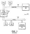
from main memory. As shown in Figure 1, a conventional DVMA system
100 utilizes an I/O Memory Management Unit "I/O MMU" 110, sometimes
referred to as an I/O Translation Lookahead Buffer, to translate virtual
addresses to physical addresses utilized by main memory 120. As shown, the
I/O MMU 110 is implemented within a bridge element 130 that couples an
I/O bus 140 and a system bus 150.
Typically, the I/O MMU 110 is often configured to contain a limited
number "r" of address translations to increase system performance with
minimal additional costs. Thus, a plurality of I/O DVMA devices 1601-160i
("i" being a whole number, i≥2) are restricted to collectively use at most "r"
virtual pages without mitigating system performance. If a requested address
translation is not contained within the I/O MMU 110, resulting in an I/O
MMU "miss", the requested address translation must be fetched from main
memory 120 which contains all potential address translations. Of course,
such fetching reduces system performance.
With the emergence of multi-media communications, networks are
now being required to support multiple data types. As a result, network
manufacturers are tending to concentrate their efforts toward asynchronous
transfer mode ("ATM") networks. In ATM networks, a large number of
virtual channels, perhaps hundreds, can be in operation simultaneously.
Hence, if the DVMA system 100 is configured to support an ATM network
coupled to I/O network interface logic 170, it would experience significant
performance degradation caused by' excessive fetching of address translations
from main memory.
To substantially avoid performance degradation, an address translation
unit ("ATU") may be implemented within a Network Interface Circuit
("NIC"). The ATU would contain a set of virtual-to-physical address
translations, whereby providing an ability to bypass the I/O MMU. These
address translations are modifiable, and thus, would require a "flush"
operation scheme to remove address translations that no longer reflect
current or active translations. This is necessary to maintain coherency.
Although system software normally has the responsibility of issuing
and controlling flush operations, it requires intensive system and code
analysis to remove code related to superfluous flush operations or to add code
to support requisite flush operations that were not previously coded. Such
intensive system and code analysis is prevalent, especially during
development and initial placement in the market when flaws in performance
can have substantial adverse effects on the success of the product.
Hence, it would be advantageous to develop hardware circuitry to at
least assist system software by checking for the existence of a particular virtual
page in the ATU before loading a new address translation for that page. This
circuitry would detect missed software flush operations, which would be
especially useful during system software development.
SUMMARY OF THE INVENTION
The present invention relates to a flush check circuit which is
configured to determine, prior to loading in an address translation into an
address translation unit, whether a virtual page number associated with the
address translation is still contained in memory of an address translation
unit. This flush check circuit assists system software to detect missed software
flush operations. Such operations would be especially useful during system
development.
BRIEF DESCRIPTION OF THE DRAWINGS
The features and advantages of the present invention will become
apparent from the following detailed description of the present invention in
which:
DESCRIPTION OF THE PREFERRED EMBODIMENT
In the following detailed description, the present invention describes
circuitry and a method for maintaining and ensuring coherency of address
translations contained in an address translation unit ("ATU"), preferably
implemented on a Network Interface Card ("NIC"). The NIC is adapted to an
I/O bus of an electronic system to interconnect the electronic system to an
asynchronous transfer mode ("ATM") network supporting a plurality of
virtual channels.
A number of terms are frequently used herein to describe certain
control circuits and binary representations which are defined herein. A
"word" is preferably 4 bytes (32-bits) in length, but may be any "2x" byte in
length (where x ≥ 0). A "packet" is a plurality of words stored, transmitted or
received in succession. An "address translation" is a mapping between a
virtual address and a physical address. A "flush" operation is a removal of an
address translation from one or more storage locations. The term "asserted"
is defined as the activation or setting of a preselected logic value. Moreover, a
"virtual address" may be construed as the entire virtual address or a portion
thereof (e.g., a virtual page number). Likewise, a "physical address" may be
construed as the entire physical address or a portion thereof (e.g., a physical
page number).
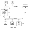
Referring to Figure 2A, an embodiment of an electronic system 200
such as, for example, a workstation manufactured by Sun Microsystems of
Mountain View, California, is illustrated. The electronic system 200 operates
as a DVMA system, although it is contemplated that the present invention
may function in conjunction with a DMA type system.
As shown, the electronic system 200 comprises one or more
multiprocessors 2101-210j ("j" being whole number, j≥1) coupled to main
memory 220 through a memory bus 230 to enable communications
therebetween. The system bus 230 is further coupled to a bridge element 240,
including an I/O MMU 250, to enable communications between components
coupled to the system bus 230 (e.g., main memory 220, microprocessor(s) 2101-210j,
etc.) and a plurality of I/O devices 2601-260k ("k" being whole number,
k≥2) coupled to an I/O bus 270. The I/O bus 270 may include, but is not
limited to, a Peripheral Component Interconnect ("PCI") bus developed by
Intel Corporation of Santa Clara, California. For example, the PCI bus may
support 64-bit address/data propagation at approximately 66 megahertz
("MHz") or 32-bit address/data propagation at approximately 33 MHz.
Although not shown, the main memory 220 includes a plurality of free
memory buffers, a Receive ("RX") descriptor ring and a RX Completion ring
to support RX operations (not shown). Likewise, there are similar elements
to support Transmit ("TX") operations. Normally, the buffers are storage
locations consecutively addressed in virtual memory, but are not necessarily
contiguous in physical memory. The buffers may be of various sizes,
occupying one or more virtual pages. Each descriptor ring includes a plurality
of descriptors, one of these descriptors being shown in Figure 2B.
Referring now to Figure 2B, a sample descriptor format 289, which is a
basic data structure that can be used by a Segment and Reassembly ("SAR")
unit to transport packet data between main memory 220 and the network, is
shown. In one embodiment, descriptors are arranged (64 bytes apart between
each descriptor) in a ring structure (which is not shown). These descriptors
point to a set of data packets to be sent to the network (in the transmit case) or
the descriptors point to a set of free memory buffers to hold incoming packets
(in a receive case). In one embodiment, each descriptor is of a fixed length
and comprises a plurality of words, ranging between three and sixteen
contiguous 32-bit words. The descriptors are placed consecutively in virtual
memory in a ring structure. Each of these descriptors, which are located in
main memory, point to a data buffer (in the transmit ("TX") case) which is
also located in main memory.
As shown in block 271 of the descriptor 289, word 0 contains
application specific control bits. Block 273 illustrates that word 1 contains a
virtual address ("VA") pointer which points to the beginning of a data buffer.
Block 275 shows that word 2 of the descriptor 289 contains application specific
information. The end of the descriptor 277 and 279 contains information on
the physical page location of the physical address ("PA") that maps to the
virtual address contained in block 273 and associated with this descriptor 289.
Block 277 illustrates that word "P" contains a translation entry 1 for the first
physical page. Each physical page of the physical address contains its own
entry. In one embodiment, the last word "P + K", where "P" is a
predetermined number greater than 2, and "K" is equal to the number of
pages the data buffer spans -1 as illustrated by block 279. If a data buffer spans
ten pages, then there will be ten translation entries at the end of descriptor
289. Thus, caching the physical address of objects greater than one page size is
supported by embedding multiple translations within a descriptor.
A sample physical translation format 281 is also shown in Figure 2B.
In one embodiment, this format 281 includes a valid bit 283, protection bits
285 and the actual physical page bits 287. The valid bit 283, in the descriptor,
determines if a specific translation entry will be placed into the ATU (if valid
bit 283 is set) or ignored (if valid bit 283 is cleared). The protection bits 285 are
transferred through control line 560 of Figure 5 in determining whether a
page is accessible using the ATU's physical translation for the virtual address.
For instance, a read-only page can be protected from writes with a read only
page protection bit. The physical page bits 287 provide the virtual to physical
address mapping for the corresponding portion of the data buffer in virtual
address space. The data buffer pointed to by the data buffer pointer 273 can
span one or more virtual pages and are not necessarily contiguously placed in
physical memory.
Referring to Figure 3, one of the plurality of I/O devices, for example
I/O device 260k, includes a Network Interface Circuit ("NIC"). The NIC 260k
includes I/O bus interface logic 300 and an ATM core 310, both of which
collectively operate to transfer data between the electronic system and other
remotely located electronic systems through multiple virtual channels
normally utilizing full duplex media 320. The media 320 may include optical
fiber, twisted pair or any other high speed communication medium normally
supporting a transfer rate of 155 million bits per second ("Mbps"), 622 Mbps,
or even at speeds faster than 622 Mbps.
The ATM core 310 features a segmentation and reassembly ("SAR")
unit 311 which facilitates segmentation and reassembly of data cells (e.g., a
standard ATM cell absent a checksum byte) and utilizes off-chip memory 330
for storage. The ATM core 310 exchanges data cells with an ATM/physical
interface 340 conforming to the well-known Universal Test and Operations
Physical Interface for ATM ("UTOPIA") standard. The ATM/physical
interface 340 is positioned to insert a checksum in a header of an out-going
data cell to produce an ATM cell or to calculate whether the checksum of an
in-coming ATM cell is correct, and if so, removing the checksum before
transferring the data cell into the ATM core 310. A physical layer 350 is
implemented for proper electrical voltage line termination. A description of
the ATM core may be found in a co-pending U.S. patent application entitled
"Method and Apparatus for Coordinating Data Transfer Between Hardware
and Software" (Application No. 08/499,317; filed July 7, 1996) by Rasoul
Oskouy and Denton E. Gentry. That U.S. patent application is owned by
Assignee of the present application.
For ATM cell transmission, the ATM core 310 is initially provided a
starting location of the TX descriptor ring. The ATM core 310 fetches the first
TX descriptor to obtain the virtual address of the data buffer associated with
the first TX descriptor. Next, the data buffer is accessed to propagate data into
the SAR unit 311 for segmentation into one or more ATM cells transmitted
through the physical media 320. After transmission of the ATM cell(s) (or at
least storage of the data in local buffers of SAR unit 311), the SAR unit 311
may acknowledge completion by writing status information to the TX
completion descriptor ring and generating an interrupt to the system to alert
the processor accordingly.
During reception, incoming ATM cells are reassembled into packets of
data which are subsequently stored in free memory buffers indicated by a
virtual address pointer contained in its corresponding RX descriptor.
Referring now to Figure 4, an embodiment of the I/O bus interface
logic 300 coupled to the I/O bus 270 (e.g., PCI bus with a 64-bit address/data
lines operating at approximately 66 MHz for this embodiment) is shown. The
I/O bus interface logic 300 includes I/O registers and transceivers 400 (e.g., PCI
I/0 registers and transceivers) coupled to a slave interface device 410 via an
I/O bus line 415. The slave interface device 410 may include an ATU control
register (not shown) used to control various features of the ATU. Moreover,
the I/O bus interface logic 300 includes one or more read buffers 420 via an
input bus 425, as well as one or more write buffers 430, and a master address
generation unit 440. Although not shown, the input bus 425 is further
coupled to the master address generation unit 440, namely a FIFO storage
element as shown in Figure 5, to receive descriptor related information. The
read buffer(s) 420 is (are) used to temporarily store information from the I/O
bus 270 while the write buffer(s) 430 is (are) used to temporarily store
information via a write data path from the SAR unit.
Implemented within the master address generation unit 440 is an
address translation unit ("ATU") 450 that receives information from the SAR
unit 311 of the ATM Core. This information includes the virtual address to
be translated, the size of the address and the type of access (e.g., access to
descriptor ring or buffer). The presence of the ATU 450 allows the electronic
system to (i) translate the virtual address into a physical address and
subsequently bypass the I/O MMU 250 of Figure 2A, or (ii) transmit the
virtual address to the I/O MMU 250 of Figure 2A.
Referring now to Figure 5, an embodiment of the ATU 450 is shown.
The ATU 450 may be configured to be fully associative. However, it is
contemplated that another memory access scheme, such as direct mapped or
N-way associative, may be utilized in order to meet a desired translation hit
rate.
The ATU 450 includes a content addressable memory ("CAM")
element 500 and random access memory ("RAM") element 502, which
collectively contain "n" address translations ("n" being a whole number,
n≥1). More specifically, the CAM element 500 includes logic that supports
loading of a virtual address and control information in one of "n" entries as
well as performing address lookup searches of the entries. The control
information may include a CAM Valid bit indicating, when set, that the entry
contains a virtual address currently being used for address translations. The
CAM element 500 further includes (i) a plurality of input ports and (ii) a
plurality of output ports.
The plurality of input ports are used to load address and control
information into the entries of the CAM element 500. As shown, there are
five (5) input ports used to load information into the CAM element. The first
input port is a data input ("Din") port used for loading a selected virtual
address provided by a select element (e.g., MUX 505) via address lines 529.
The second input port is an address update ("Aupdate") port for receiving, via
CAM Update address lines 530 an entry number of the entry selected to be
loaded with the virtual address on the data lines 529. The third input port is a
command ("CAM command") port from which the CAM element 500
receives command information to control its operation via command lines
524. Types of commands include, but are not limited to "Translate" or
"Update". In addition, the fourth input port is an entry valid ("Valid") port
through which a control line 528, representative of the CAM Valid bit of an
entry addressed by the Aupdate port, is asserted or de-asserted depending on if
the entry is "valid" (e.g., in a "valid" state or currently being used), or
"invalid" (e.g., in an "invalid" state or stale). The fifth input port is an
address lookup ("Alookup") port from which the CAM element 500 receives a
virtual address (e.g., page number) via lookup address lines 532 to be
compared with the virtual addresses stored in each of its entries. If a match
occurs, an output ("Hit") port and its control line (referred to as "CAM_Hit"
536) is asserted (i.e., an active signal is produced). As a result, a signal out
("Sout") port propagates the entry number of the CAM entry containing the
virtual address through signal lines 534.
Referring still to Figure 5, the RAM element 502 is configured to
contain the corresponding physical address for the virtual address stored in
CAM element 500. Similar to the CAM element 500, the RAM element 502
includes a plurality of input and output ports. More particularly, the RAM
element 502 includes a data input ("Din") port used for loading, via data lines
548, a physical address corresponding to the virtual address loaded into the
CAM element 500. The RAM element 502 further includes an address ("A")
port for entry lookups and entry updates. A write enable ("Wen") port is used
to distinguish between an entry update (e.g., Wen line 550 being asserted) and
entry lookup (e.g., Wen line 550 being de-asserted). In addition, the RAM
element 502 includes a first data out ("Dout1") port to output the physical
address corresponding to the virtual address being translated or searched, via
address lines 562 and a second data out ("Dout2") port to output write
protection information contained in the selected entry via control line 560.
Moreover, the RAM element 502 includes an entry' status ("Estat") port to
provide information indicating which entries of the CAM and RAM
elements has been accessed via Entry status lines 572.
In addition to the CAM and RAM elements 500 and 502, the ATU 450
further includes a first group of control logic that controls the loading and
flushing of the address translations, and a second group of control logic that
controls whether the ATU 400 should output a virtual or physical address via
address lines 516. An indicator used to bypass I/O MMU may include, but is
not limited to, a high order address bit being set or cleared, a specific subset of
the address space being accessed, etc. For example, in one embodiment, the
bridge element 240 such as that shown in Figure 2A provides an address
range within the 64-bit address space which when accessed treats the lower 41
bits of the address as a physical address.
As shown, the first group of control logic includes a plurality of select
elements 504-506 and 508 (e.g., multiple input multiplexers), and a first-in,
first-out ("FIFO") storage element 514. The FIFO storage element 514 is used
to temporarily store virtual/physical address translations as they are read
from the input bus 425 during descriptor fetches.
The plurality of select elements 504-506 and 508 are controlled by ATU
control state machine ("ATUCSM") 580 through control lines 581-584. A first
select element 504 is coupled to the Alookup port of the CAM element 500 via
lookup address lines 532 in order to route the virtual address to be searched
within the CAM element 500. This select element receives as input virtual
addresses (or virtual page numbers) through software flush address lines
("SW Flush address lines") hardware flush lines 518, ("HW Flush address
lines") 520 and address lines 522 for usual translation loading. The second
select element 505 is coupled to the Din port of the CAM element 500 via data
lines 529 to load either a (i) virtual address obtained from a descriptor fetch
via lines 554, or alternatively, (ii) a virtual address of a data buffer specified
manually by software writing the buffer's virtual address into CAM element
500. This is an access of the slave interface device 410 resulting in that virtual
address being placed on lines 558. A third select element 506 is coupled to the
address port via address lines 546 to transmit therein either a RAM Update
address via a RAM Update address line 538 or an entry number output from
the CAM 502 element through the Sout port via signal lines 534. The fourth
select element 508 is coupled to the Din port via address lines 548 to input
physical addresses and control information from lines 540 and 544.
The second group of control logic includes a hit/miss logic circuit 512
and a fifth select element 510. The hit/miss logic circuit 512 is combinatorial
logic configured to control whether the fifth select element 510 outputs onto
the address lines 516 (i) a translated physical address received from lines 562
or (ii) the virtual address for lines 526 to be subsequently translated by the I/O
MMU. Such control is performed by the assertion or de-assertion of an
ATU_Hit control line 564.
The translated physical address is output from the fifth select element
510 under all conditions unless (i) the CAM_Hit line 536 is not asserted
thereby indicating a "lookup miss", (ii) the ATU 450 is disabled by System
software not asserting an ATU enable line 566, (iii) a cycle status line 568 is
not asserted indicating that this particular translation should be avoided, or
(iv) the protection bits 560 signify that the cycle in progress is prohibited due
to reasons including, but not limited to, an attempted write access of a read-only
page.
Since the ATU 450 is implemented with memory supporting a limited
number of address translations which are modifiable, it would be
advantageous to implement circuitry to support a number of functions,
including but not limited to, (i) assisting system software by checking the
existence of a particular virtual page in the ATU before loading a new
translation with that page; (ii) self-verification that it has invalidated an entry
associated with a particular virtual page before loading a new address
translation associated with that particular page; and (iii) reporting missed
flush operations or entry invalidations via interrupt or status register polling.
Referring now to Figure 6, a preferred embodiment of the update
control circuit 600 is shown, wherein the update control circuit 600 comprises
an ATU replacement element 610, a CAM Address Encode circuit 620, a select
element 630, an increment circuit 640 and a CAM Address Decode circuit 650.
The update control circuit 600 is coupled to the CAM Update Address control
lines 530 to select which entry of the CAM element is to be loaded with a
virtual address from either the I/O bus line 415 or the input bus 425 of Figures
4 and 5. It is contemplated, however, that the RAM Update address lines 538
may be coupled to the CAM Update address lines 530 in order to receive the
same entry number selections to maintain operation coherency.
The ATU replacement element 610 is a plurality of storage elements
(e.g., "n" storage elements 6111-611n), each storage element uniquely
corresponding to one CAM entry. As shown in Figure 6, each of the plurality
of storage elements 6111-611n is implemented as a 1-bit register being clocked
at a predetermined frequency "CLK" through clock line 612. It is
contemplated, however, that the storage elements 6111-611n may include
other types of storage devices besides 1-bit registers.
When one of a plurality of clock enable control lines 6141,.., or 614n
(e.g., clock enable control line 6141) is asserted by' the CAM Address Decode
circuit 650, a storage element associated with the clock enable control line
(e.g., storage element 6111) is "set" by loading a CAM Valid bit value therein.
The CAM Valid bit value (e.g., a logic "1") is loaded via a data input line 613
in order to represent that the CAM and RAM entries, corresponding to the
storage element, contain a valid address translation. Thus, the plurality of
storage elements 6111-611n provide an external copy of the state of each CAM
entry.
The CAM Address Encode circuit 620 is combinatorial logic coupled to
the ATU replacement element 610 in order to monitor the contents of each of
the plurality of storage elements 6111-611n. Typically, this monitoring is
performed by reading the contents of the storage elements 6111-611n provided
through data lines 6151-615n and then ascertaining if at least one storage
element 6111,.., or 611n is not set (e.g., determining if at least one CAM entry
is not currently being used for translations). The CAM Address Encode circuit
620 further includes an ATU_Full select line 621 and a number (e.g., log2(n))
of data input lines 631 (referred to as "E_Num" lines 631) of the select
element 630.
Upon detecting at least one storage element that is not set (referred to
as an "empty storage element"), the CAM Address Encode circuit 620
performs three operations. Namely, the CAM Address Encode circuit 620 (i)
selects the empty storage element, (i) outputs an entry number, which
represents the location of the empty storage element in the ATU replacement
element 610, to the select element 630 via the E_Num lines 631, and (iii) de-asserts
the ATU_Full select line 621. Thereafter, the entry number is
transferred through the select element 630 to the CAM Update address lines
530, thereby loading the virtual address of the address translations in an entry
of the CAM element corresponding to the entry number. Moreover, the
physical address of the address translation is preferably loaded in an entry of
the RAM element corresponding to the entry number. However, if there
does not exist any empty storage elements, the CAM Address Encode circuit
620 asserts the ATU_Full select line 621 thereby controlling the select element
630 to output a count value produced by the increment circuit 640 as described
below.
As further shown, the select element 630 is a multi-input multiplexer,
or a group of multi-input multiplexers coupled together to transmit one of a
plurality of data inputs. The data inputs of the select element 630 include the
entry number via the E_Num lines 631, a "flush entry number" (provided by
the flush control circuit 700 of Figure 7) via input lines 632 (i.e., "Flush"
lines), and a count value from the increment circuit 640 via input lines 633
(i.e., "Count" lines). The selection of one of these inputs as the output is
controlled by the assertion or de-assertion of the ATU_Full select line 621 by
the CAM Address Encode circuit 620 and whether or not the ATU control
state machine (not shown) are supporting a flush operation represented by
assertion or de-assertion of a Flush Invalidate Update control line 622.
If all of the address translations are actively being used, as signified by
the all of the CAM Valid bits for the CAM entries and storage elements 6111-611n
of the ATU replacement element 610 being "set", the ATU_Full select
line 621 is asserted. Assertion of the ATU_Full select line 621 causes the
count value, provided by the increment circuit 640, to be output from the
select element 630 through the CAM Update address lines 530. The count
value represents which entries of the CAM and RAM elements are to be
loaded with the new address translation. The increment circuit 640 includes a
"Modulo n" counter 641 which is incremented and enabled when the
ATU_Full select line 621 is asserted and a CAM Update command is
produced by the ATU control state machine 580 of Figure 5.
The CAM Address Decode circuit 650 includes combinatorial logic
coupled to the select element 630 through a feedback loop 651 in order to
update the contents of the ATU replacement element 610 based on a
modification to a CAM entry in a prior cycle. This entry modification is
represented by the entry number, the flush entry number, or the count value
being transmitted through the CAM Update address lines 530. The CAM
Address Decode circuit 650 is further coupled to the ATU control state
machine (not shown) to monitor when a CAM Update command is asserted
via CAM command lines 524, and in response, to assert a clock enable control
line 6141,..., or 614n associated with the storage element 6111,..., or 611n that
corresponds to the CAM entry being updated.
Referring now to Figure 7, an embodiment of the flush control circuit
700 is shown. The flush control circuit 700 comprises a first circuit 710
coupled to the HW Flush address lines 520 of the ATU and a second circuit
740 coupled to the address lines 522 and the Flush lines 632 (see also Figures 5-6).
The first circuit 710 is configured to propagate a virtual page number to
the CAM upon detection of conditions (e.g., page crossings, end-of-packet, etc.)
in which a flush operation by hardware would enhance system performance.
The second circuit 740 is configured to perform two operations;
namely, (i) a flush check when enabled and before loading a new translation
by the update circuit 600, and (ii) a flush operation on a CAM entry. Flush
checking is enabled by setting a flush check bit "FLSH_CHK" in the ATU
control register. As mentioned above, the ATU control register may be one of
the I/O registers implemented in the slave interface device 410 of the I/O bus
interface logic 400 of Figure 4.
As shown in Figure 7, the second circuit 740 includes a flush check
circuit 750 configured to perform a check on the CAM entries before loading a
new address translation. The flush check circuit 750 includes flush
management logic 755 configured to temporarily contain a virtual address
(e.g., a virtual page number) of the address translation to be loaded. During a
flush check operation and if the FLSH_CHK bit is set, the status of which are
indicated by signal lines 756-757, the flush management logic 755 activates the
select line 581 for the first select element 504 in order to allow the virtual page
number from the FIFO storage element 514 to flow therethrough. The virtual
page number is routed from address lines 599 to the address lines 532 under
the control of the ATU control state machine 580.
If the virtual page number is not found in a CAM entry, the new
translation is loaded under the usual translation procedure as discussed
above. However, if the virtual page number is located upon searching the
contents of the CAM entries, the new address translation is not loaded into
the CAM entry. Instead, an error signal is generated by the ATU control state
machine 580 to the processor via an interrupt line (not shown) or to a register
accessible by the processor. The presence of the virtual page number indicates
that it was not flushed out by software after a previous establishment of the
virtual page-to-physical mapping. If hardware is responsible for flushing the
entry by invalidating the entry, the presence of the virtual page number
indicates the hardware did not operate appropriately. This indicates that
invalid translation has been uncovered causing the error signal to be asserted.
It is contemplated that the hardware may include the flush management logic
755 cooperating with a set of storage elements 765 and the update circuit 600 as
described in the concurrently filed U.S. patent application entitled "A Circuit
and Method for Replacement of Address Translations" (Application No.
08/ ; Attorney Docket No. 082225.P1701) incorporated herewith by
reference.
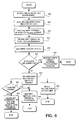
Referring now to Figure 8, an embodiment of the operations of the
flush check is described. The flush check is affiliated with a hardware
translation load since the virtual address of the new address translation
should not be contained in I/O MMU because it is a new virtual-to-physical
mapping. If the address is present, it indicates that the virtual address was not
"flushed" previously. The flush check may be utilized as a debug operation.
As shown in Step 800, a flush check mode is established by setting the
FLSH_CHK bit in the ATU control register. A hardware translation load
trigger, as shown in step 805, takes the ATU control state machine out of its
idle state. In Step 810, the virtual page number from the FIFO storage
element 514 is placed on the Alookup port of the CAM element. In step 815, a
TRANSLATE command is sent to CAM element 500. The next step 820 is the
ATU monitors the CAM_Hit signal. If a CAM_Hit signal is de-asserted,
indicating a "lookup miss", there is no further action required and the
translation is to be loaded as normal (Steps 825 and 830).
However, if the CAM_Hit signal is asserted (e.g., a logic "1"), an
"unflushed" translation was found (Step 835). As a result, the ATU may
generate an interrupt to one or more microprocessor(s) of the electronic
system which are shown in Figure 2A (Step 840). Optionally, as shown in
Steps 845 and 850), the ATU could record the virtual address transferred
issuing on lines 562. Additionally, the ATU may generate the interrupt along
with recordation of the address translation as shown in Step 840. Another
option is to make the translation an "ATU miss" (e.g., cause the ATU_Hit
signal to be de-asserted) so that a virtual address is issued on address lines 516
to the I/O MMU 250. Thus, the I/O MMU 250 is required to handle the error
instead of the ATU (Step 855).
The present invention described herein may be designed in many
different methods and using many different configurations. While the
present invention has been described in terms of various embodiments, other
embodiments may come to mind to those skilled in the art without departing
from the spirit and scope of the present invention. The invention should,
therefore, be measured in terms of the claims which follows.