EP0826237B1 - METHOD OF FORMING A Ta205 DIELECTRIC LAYER - Google Patents
METHOD OF FORMING A Ta205 DIELECTRIC LAYER Download PDFInfo
- Publication number
- EP0826237B1 EP0826237B1 EP96920294A EP96920294A EP0826237B1 EP 0826237 B1 EP0826237 B1 EP 0826237B1 EP 96920294 A EP96920294 A EP 96920294A EP 96920294 A EP96920294 A EP 96920294A EP 0826237 B1 EP0826237 B1 EP 0826237B1
- Authority
- EP
- European Patent Office
- Prior art keywords
- capacitor
- electrically conductive
- diffusion barrier
- dielectric layer
- barrier layer
- Prior art date
- Legal status (The legal status is an assumption and is not a legal conclusion. Google has not performed a legal analysis and makes no representation as to the accuracy of the status listed.)
- Expired - Lifetime
Links
Images
Classifications
-
- H—ELECTRICITY
- H01—ELECTRIC ELEMENTS
- H01L—SEMICONDUCTOR DEVICES NOT COVERED BY CLASS H10
- H01L21/00—Processes or apparatus adapted for the manufacture or treatment of semiconductor or solid state devices or of parts thereof
- H01L21/70—Manufacture or treatment of devices consisting of a plurality of solid state components formed in or on a common substrate or of parts thereof; Manufacture of integrated circuit devices or of parts thereof
-
- H—ELECTRICITY
- H01—ELECTRIC ELEMENTS
- H01L—SEMICONDUCTOR DEVICES NOT COVERED BY CLASS H10
- H01L28/00—Passive two-terminal components without a potential-jump or surface barrier for integrated circuits; Details thereof; Multistep manufacturing processes therefor
- H01L28/40—Capacitors
- H01L28/55—Capacitors with a dielectric comprising a perovskite structure material
- H01L28/56—Capacitors with a dielectric comprising a perovskite structure material the dielectric comprising two or more layers, e.g. comprising buffer layers, seed layers, gradient layers
-
- H—ELECTRICITY
- H01—ELECTRIC ELEMENTS
- H01L—SEMICONDUCTOR DEVICES NOT COVERED BY CLASS H10
- H01L28/00—Passive two-terminal components without a potential-jump or surface barrier for integrated circuits; Details thereof; Multistep manufacturing processes therefor
- H01L28/40—Capacitors
Definitions
- This invention relates to methods of forming a capacitor having a Ta 2 O 5 dielectric layer, to methods of forming a Ta 2 O 5 dielectric layer, and to capacitor constructions.
- DRAMs increase in memory cell density, there is a continuing challenge to maintain sufficiently high storage capacitance despite decreasing cell area. Additionally, there is a continuing goal to further decrease cell area.
- One principal way of increasing cell capacitance is through cell structure techniques. Such techniques include three-dimensional cell capacitors, such as trenched or stacked capacitors. Yet as feature size continues to become smaller and smaller, development of improved materials for cell dielectrics as well as the cell structure are important.
- the feature size of 256 Mb DRAMs will be on the order of 0.25 micron, and conventional dielectrics such as SiO 2 and Si 3 N 4 might not be suitable because of small dielectric constants.
- Ta 2 O 5 films are considered to be very promising cell dielectrics layers, as the dielectric constant of Ta 2 O 5 is approximately three times that of Si 3 N 4 .
- Proposed prior art capacitor constructions include the use of Ta 2 O 5 as a capacitor dielectric layer, in combination with an overlying predominately crystalline TiN electrode or other layer.
- diffusion relative to the tantalum layer is problematic in the resultant capacitor construction.
- tantalum from the Ta 2 O 5 tends to undesirably out-diffuse from the dielectric layer.
- materials from the adjacent conductive capacitor plates can diffuse into the tantalum layer. In either event, the dielectric properties of the Ta 2 O 5 layer are adversely affected in a less than predictable or an uncontrollable manner.
- a method of forming a capacitor is given in claim 2.
- a method of forming a structure comprising a dielectric layer in accordance with the invention is given in claim 1.
- a capacitor in accordance with a further aspect of the invention is given in claim 9.
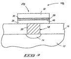
- a semiconductor wafer fragment is indicated generally with reference numeral 10.
- Such comprises a bulk silicon substrate 12 having a conductive diffusion area 14 formed therein.
- An insulating layer 16 typically borophosphosilicate glass (BPSG), is provided over substrate 12, with a contact opening 18 having been previously provided therein to diffusion area 14.
- a conductive material 20 fills contact opening 18, with material 20 and oxide layer 16 having been planarized as shown.
- Material 20 might be any suitable conductive material, such as tungsten or conductively doped polysilicon.
- a capacitor construction 25 is provided atop layer 16 and plug 20, with conductive plug 20 constituting a node to which electrical connection to capacitor 25 is made.
- Capacitor 25 comprises a first electrically conductive capacitor plate 26 which has been provided and patterned over node 20.
- An example and preferred material is conductively doped polysilicon, provided to a thickness of 1000 Angstroms for 256 Mb density.
- a capacitor dielectric layer 28 of Ta 2 O 5 is provided over first electrically conductive capacitor plate 26.
- An example process for depositing layer 28 is by low pressure chemical vapor deposition at 450° C using Ta(OC 2 H 5 ) 5 and oxygen as precursors. Ta(OC 2 H 5 ) 5 can be vaporized at 170° C, and introduced into a reactor chamber using argon or another suitable carrier gas.
- densification by rapid thermal annealing in a dry oxygen atmosphere at a temperature ranging from 700° C to 900° C is utilized.
- the polysilicon surface of lower capacitor plate 26 is cleaned by an in situ HF dip prior to provision of the Ta 2 O 5 .
- Rapid thermal nitrogen treatment can also be carried out immediately prior to Ta 2 O 5 deposition, such as at 900° C for 60 seconds in NH 3 .
- An example and preferred thickness for layer 28 in accordance with 256 Mb integration is 100 Angstroms.
- a predominately amorphous diffusion barrier layer 30 is provided over Ta 2 O 5 dielectric layer 28.
- Such layer is preferably electrically conductive, with an example and preferred thickness for 256 Mb integration being 200 Angstroms.
- the layer 30 is predominately amorphous TiC x N y O z deposited by metal organic chemical vapor deposition (MOCVD), where "x" is in the range of from 0.01 to 0.5, and “y” is in the range of from 0.99 to 0.5, and “z” is in the range of from 0 to 0.3, with the sum of "x", "y” and “z” equalling about 1.0.
- a preferred metal organic precursor for such deposition is Ti(NR 2 ) 4 , where R is selected from the group consisting of H and a carbon containing radical.
- the amorphous diffusion barrier layer comprising TiC x N y O z material is a barrier. to out-diffusion of tantalum from the Ta 2 O 5 layer.
- oxygen can undesirably become incorporated in the deposited film when it is exposed to oxygen, even ambient air. This incorporated oxygen undesirably affects conductivity. Accordingly, exposure to oxygen is preferably minimized until the subject film is covered by subsequent layers which can effectively act as a barrier to oxygen incorporation.
- second electrically conductive capacitor plate 32 is provided outwardly of diffusion barrier layer 30, such that Ta 2 O 5 dielectric layer 28 is positioned between the first and second electrically conductive plates. Accordingly, second electrically conductive capacitor plate 32 constitutes a discrete, second electrically conductive capacitor plate provided over the amorphous diffusion barrier layer 30.
- An example and preferred material for second capacitor plate 32 is polysilicon, with 1000 Angstroms being an example preferred thickness for 256 Mb integration.
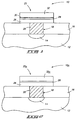
- Fig. 2 illustrates an alternate embodiment capacitor construction and method in accordance with the invention.
- Wafer fragment 10a comprises a capacitor construction 25a differing from the first described embodiment in provision of a predominately amorphous, electrically conductive second capacitor plate 32a which functions as an inherent amorphous diffusion barrier layer.
- the material is the previously described metal organic chemical vapor deposited TiC x N y O z which is provided to a thickness which is effective to form the predominant portion (the entire portion, as shown) of second electrically conductive capacitor plate 32a.
- both of plates 32 and 26 might be provided to constitute a conductive inherently amorphous diffusion barrier layer, such as the MOCVD TiC x N y O z .
- Fig. 3 illustrates yet another alternate embodiment capacitor construction and method. Again, like numerals from the first described embodiment are utilized where appropriate, with differences being indicated by different numerals or with the suffix "b".
- Wafer fragment 10b includes a capacitor construction 25b having the same first and second capacitor plates 26 and 32, respectively, of the first described embodiment. However, a pair of predominately amorphous diffusion barrier layers 30 and 40 are provided to encapsulate Ta 2 O 5 dielectric layer 28 to prevent tantalum out-diffusion.
- the invention was reduced to practice in a study of three types of rapid thermal nitrogen annealed polysilicon films having Ta 2 O 5 films thereatop, with different overlying titanium nitride or titanium carbonitride layers being deposited.
- the inventive constructions were deposited by metal organic chemical vapor deposition of a TiC x N y O z film deposited from tetrakisdimethylamido titanium (TDMAT) at 450° C, and 0.5 Torr in a cold wall chemical vapor deposition reactor. These wafers were compared with two non-inventive deposited titanium nitride layers. These two non-invention layers were deposited by chemical vapor deposition and by sputtering, respectively.
- the CVD TiN films were formed by reacting TiCl 4 and NH 3 at 600° C (i.e., non-MOCVD) in a low pressure chemical vapor deposition reactor.
- the sputtered TiN films were formed by reactive sputtering of Ti in an Ar-N 2 ambient at 0.014 Torr. The substrates were heated to 400° C during deposition.
- an additional capping layer of sputtered TiN was deposited for protection against oxidation during plasma steps used to remove photoresist.
- the sputter deposited and CVD TiN films using TiCl 4 and NH 3 were crystalline, while the MOCVD films of the invention are substantially amorphous.
Abstract
Description
- This invention relates to methods of forming a capacitor having a Ta2O5 dielectric layer, to methods of forming a Ta2O5 dielectric layer, and to capacitor constructions.
- As DRAMs increase in memory cell density, there is a continuing challenge to maintain sufficiently high storage capacitance despite decreasing cell area. Additionally, there is a continuing goal to further decrease cell area. One principal way of increasing cell capacitance is through cell structure techniques. Such techniques include three-dimensional cell capacitors, such as trenched or stacked capacitors. Yet as feature size continues to become smaller and smaller, development of improved materials for cell dielectrics as well as the cell structure are important. The feature size of 256 Mb DRAMs will be on the order of 0.25 micron, and conventional dielectrics such as SiO2 and Si3N4 might not be suitable because of small dielectric constants.
- Chemical vapor deposited (CVD) Ta2O5 films are considered to be very promising cell dielectrics layers, as the dielectric constant of Ta2O5 is approximately three times that of Si3N4. Proposed prior art capacitor constructions include the use of Ta2O5 as a capacitor dielectric layer, in combination with an overlying predominately crystalline TiN electrode or other layer. However, diffusion relative to the tantalum layer is problematic in the resultant capacitor construction. For example, tantalum from the Ta2O5 tends to undesirably out-diffuse from the dielectric layer. Further, materials from the adjacent conductive capacitor plates can diffuse into the tantalum layer. In either event, the dielectric properties of the Ta2O5 layer are adversely affected in a less than predictable or an uncontrollable manner.
- Preferred embodiments of the invention are described below with reference to the following accompanying drawings.
- Fig. 1 is a diagrammatic sectional view of a semiconductor wafer fragment in accordance with the invention.
- Fig. 2 is a diagrammatic sectional view of an alternate embodiment semiconductor wafer fragment in accordance with the invention.
- Fig. 3 is a diagrammatic sectional view of yet another alternate embodiment semiconductor wafer fragment in accordance with the invention.
- A method of forming a capacitor is given in claim 2.
- A method of forming a structure comprising a dielectric layer in accordance with the invention, is given in claim 1.
- A capacitor in accordance with a further aspect of the invention is given in claim 9.
- More particularly and first with reference to Fig. 1, a semiconductor wafer fragment is indicated generally with
reference numeral 10. Such comprises abulk silicon substrate 12 having aconductive diffusion area 14 formed therein. Aninsulating layer 16, typically borophosphosilicate glass (BPSG), is provided oversubstrate 12, with a contact opening 18 having been previously provided therein todiffusion area 14. Aconductive material 20 fills contact opening 18, withmaterial 20 andoxide layer 16 having been planarized as shown.Material 20 might be any suitable conductive material, such as tungsten or conductively doped polysilicon. Acapacitor construction 25 is provided atoplayer 16 andplug 20, withconductive plug 20 constituting a node to which electrical connection tocapacitor 25 is made. -
Capacitor 25 comprises a first electricallyconductive capacitor plate 26 which has been provided and patterned overnode 20. An example and preferred material is conductively doped polysilicon, provided to a thickness of 1000 Angstroms for 256 Mb density. A capacitordielectric layer 28 of Ta2O5 is provided over first electricallyconductive capacitor plate 26. An example process for depositinglayer 28 is by low pressure chemical vapor deposition at 450° C using Ta(OC2H5)5 and oxygen as precursors. Ta(OC2H5)5 can be vaporized at 170° C, and introduced into a reactor chamber using argon or another suitable carrier gas. Subsequently, densification by rapid thermal annealing in a dry oxygen atmosphere at a temperature ranging from 700° C to 900° C is utilized. Preferably, the polysilicon surface oflower capacitor plate 26 is cleaned by an in situ HF dip prior to provision of the Ta2O5. Rapid thermal nitrogen treatment can also be carried out immediately prior to Ta2O5 deposition, such as at 900° C for 60 seconds in NH3. An example and preferred thickness forlayer 28 in accordance with 256 Mb integration is 100 Angstroms. - A predominately amorphous
diffusion barrier layer 30 is provided over Ta2O5dielectric layer 28. Such layer is preferably electrically conductive, with an example and preferred thickness for 256 Mb integration being 200 Angstroms. - The
layer 30 is predominately amorphous TiCxNyOz deposited by metal organic chemical vapor deposition (MOCVD), where "x" is in the range of from 0.01 to 0.5, and "y" is in the range of from 0.99 to 0.5, and "z" is in the range of from 0 to 0.3, with the sum of "x", "y" and "z" equalling about 1.0. A preferred metal organic precursor for such deposition is Ti(NR2)4, where R is selected from the group consisting of H and a carbon containing radical. Deposition conditions for producing such a predominately amorphous layer include from 200° C to 600° C, and from 0.1 to 100 Torr 1 Torr = 133.3 Pa. The amorphous diffusion barrier layer comprising TiCxNyOz material is a barrier. to out-diffusion of tantalum from the Ta2O5 layer. - Also most preferably, "z" will be equal to zero. Unfortunately however, oxygen can undesirably become incorporated in the deposited film when it is exposed to oxygen, even ambient air. This incorporated oxygen undesirably affects conductivity. Accordingly, exposure to oxygen is preferably minimized until the subject film is covered by subsequent layers which can effectively act as a barrier to oxygen incorporation.
- Subsequently, a second electrically
conductive capacitor plate 32 is provided outwardly ofdiffusion barrier layer 30, such that Ta2O5dielectric layer 28 is positioned between the first and second electrically conductive plates. Accordingly, second electricallyconductive capacitor plate 32 constitutes a discrete, second electrically conductive capacitor plate provided over the amorphousdiffusion barrier layer 30. An example and preferred material forsecond capacitor plate 32 is polysilicon, with 1000 Angstroms being an example preferred thickness for 256 Mb integration. - Prior art constructions and proposals for utilizing Ta2O5 as a capacitor dielectric layers suffer from the drawback of undesired out-diffusion of tantalum atoms from such layer, or diffusion of undesired components into such layer. Provision of a thin predominately amorphous diffusion barrier layer as described above facilitates maintaining integrity of the Ta2O5 layer and, accordingly, its associated desired high dielectric constant in such a small application. It has been discovered in the context of the invention that amorphous materials are better diffusion barriers due to absence of crystal grain boundaries which can provide an easy path for diffusion in polycrystalline materials.
- Fig. 2 illustrates an alternate embodiment capacitor construction and method in accordance with the invention. Like numerals from Fig. 1 have been utilized where appropriate, with differences being indicated by either different numerals, or like numerals with the suffix "a". Wafer fragment 10a comprises a capacitor construction 25a differing from the first described embodiment in provision of a predominately amorphous, electrically conductive second capacitor plate 32a which functions as an inherent amorphous diffusion barrier layer. The material is the previously described metal organic chemical vapor deposited TiCxNyOz which is provided to a thickness which is effective to form the predominant portion (the entire portion, as shown) of second electrically conductive capacitor plate 32a. Alternately, both of
plates - Fig. 3 illustrates yet another alternate embodiment capacitor construction and method. Again, like numerals from the first described embodiment are utilized where appropriate, with differences being indicated by different numerals or with the suffix "b". Wafer
fragment 10b includes acapacitor construction 25b having the same first andsecond capacitor plates diffusion barrier layers dielectric layer 28 to prevent tantalum out-diffusion. - The invention was reduced to practice in a study of three types of rapid thermal nitrogen annealed polysilicon films having Ta2O5 films thereatop, with different overlying titanium nitride or titanium carbonitride layers being deposited. The inventive constructions were deposited by metal organic chemical vapor deposition of a TiCxNyOz film deposited from tetrakisdimethylamido titanium (TDMAT) at 450° C, and 0.5 Torr in a cold wall chemical vapor deposition reactor. These wafers were compared with two non-inventive deposited titanium nitride layers. These two non-invention layers were deposited by chemical vapor deposition and by sputtering, respectively. The CVD TiN films were formed by reacting TiCl4 and NH3 at 600° C (i.e., non-MOCVD) in a low pressure chemical vapor deposition reactor. The sputtered TiN films were formed by reactive sputtering of Ti in an Ar-N2 ambient at 0.014 Torr. The substrates were heated to 400° C during deposition. On top of the CVD TiN film, and also on the inventive MOCVD films, an additional capping layer of sputtered TiN was deposited for protection against oxidation during plasma steps used to remove photoresist. The sputter deposited and CVD TiN films using TiCl4 and NH3 were crystalline, while the MOCVD films of the invention are substantially amorphous.
- Four samples of each group were prepared, out of which three were annealed at 700° C, 800° C and 900° C for thirty minutes at 7 x 10⁻⁶ Torr. With respect to the control CVD TiN films, out-diffusion of Ta into this crystalline TiN layer was observed, and to increase with increasing annealing temperature. Also with the crystalline sputtered TiN films, significant out-diffusion of tantalum into the TiN layer was observed after the 900° C anneal.
- With the amorphous MOCVD TiCxNyOz films, no out-diffusion of tantalum was observed. Twenty atomic percent of carbon and oxygen were however detected in the film. Yet, the absence of interaction of the MOCVD TiCxNyOz layers with the dielectric Ta2O5 up to 900° C makes such composite layers attractive candidates for capacitor and other dielectric layers.
Claims (16)
- A method of forming a structure comprising a dielectric layer the method comprising the following steps:forming a dielectric layer of Ta2O5 atop a substrate; andforming over the dielectric layer a predominately amorphous diffusion barrier layer to tantalum diffusion from the Ta2O5 dielectric layer by metal organic chemical vapor depositing a TiCxNyOz layer over the Ta2O5, where x is in the range of from 0.01 to 0.5, and y is in the range of from 0.99 to 0.5, and z is in the range of from 0 to 0.3, with the sum of x, y and z equalling about 1.0.
- A method of forming a capacitor comprising the following steps:forming a first electrically conductive capacitor plate over a substrate;forming a capacitor dielectric layer of Ta2O5 over the first electrically conductive capacitor plate; andforming over the dielectric layer a predominately amorphous diffusion barrier layer to tantalum diffusion from the Ta2O5 dielectric layer by metal organic chemical vapour depositing a TiCxNyOz layer over the Ta2O5, where x is in the range of from 0.01 to 0.5, and y is in the range of from 0.99 to 0.5, and z is in the range of from 0 to 0.3, with the sum of x, y and z equalling about 1.0.
- The method according to claim 1 or claim 2, wherein the diffusion barrier layer comprises predominately amorphous TiCxNyOz wherein z is 0.
- The method according to any preceding claim, wherein the diffusion barrier layer is provided at a thickness of 200 Angstroms.
- The method according to any preceding claim, wherein the diffusion barrier layer is provided to be electrically conductive.
- The method according to any preceding claim, wherein the step of metal organic chemical vapor depositing TiCxNyOz comprises utilizing a gaseous titanium organometallic precursor of the formula Ti(NR2)4, where R is selected from the group consisting of H and a carbon containing radical, and utilizing deposition conditions of from 200° C to 600° C and from 13.32 to 1.33 x 10³Pa (0.1 to 100 Torr).
- The method according to claim 2 or any claim dependent from claim 2, wherein the diffusion barrier layer is provided to be electrically conductive and to a thickness which is effective to form the predominate portion of a second electrically conductive capacitor plate.
- The method according to claim 2 or any claim dependent from claim 2, further comprising providing a discrete, second electrically conductive capacitor plate over the diffusion barrier layer.
- A capacitor comprising:a first electrically conductive capacitor plate;a capacitor dielectric layer adjacent the first electrically conductive capacitor plate, the capacitor dielectric layer comprising Ta2O5;a second electrically conductive capacitor plate, the Ta2O5 dielectric layer being positioned between the first and second electrically conductive plates; andadjacent the dielectric layer, a predominately amorphous diffusion barrier layer to tantalum diffusion from the Ta2O5 dielectric layer, the barrier layer comprising TiCxNyOz, where x is in the range of from 0.01 to 0.5, and y is in the range of from 0.99 to 0.5, and z is in the range of from 0 to 0.3, with the sum of x, y and z equalling about 1.0.
- The capacitor according to claim 9, comprising a pair of predominately amorphous diffusion barrier layers adjacent the Ta2O5 dielectric layer.
- The capacitor according to claim 9 or claim 10, wherein the or each diffusion barrier layer has a thickness of 200 Angstroms
- The capacitor according to any one of claims 9 to 11, wherein the or each amorphous diffusion barrier layer is electrically conductive.
- The capacitor according to claim 9, wherein the amorphous diffusion barrier layer is electrically conductive and constitutes a thickness which is effective to form a predominate portion of the second electrically conductive capacitor plate.
- The capacitor according to claim 10, wherein the amorphous diffusion barrier layers are electrically conductive and constitute respective thickness which are effective to form a predominate portion of the first and the second electrically conductive capacitor plates respectively.
- The capacitor according to claim 9, wherein the said amorphous diffusion barrier layer is electrically conductive, and a predominate portion of the second capacitor plate is discrete from the amorphous diffusion barrier layer.
- The capacitor according to claim 10, wherein the amorphous diffusion barrier layers are electrically conductive, and predominate portions of each of the first and second capacitor plates are discrete from the amorphous diffusion barrier layers.
Applications Claiming Priority (3)
| Application Number | Priority Date | Filing Date | Title |
|---|---|---|---|
| US444853 | 1995-05-19 | ||
| US08/444,853 US5663088A (en) | 1995-05-19 | 1995-05-19 | Method of forming a Ta2 O5 dielectric layer with amorphous diffusion barrier layer and method of forming a capacitor having a Ta2 O5 dielectric layer and amorphous diffusion barrier layer |
| PCT/US1996/007212 WO1996036993A1 (en) | 1995-05-19 | 1996-05-17 | METHOD OF FORMING A Ta2O5 DIELECTRIC LAYER |
Publications (3)
| Publication Number | Publication Date |
|---|---|
| EP0826237A1 EP0826237A1 (en) | 1998-03-04 |
| EP0826237A4 EP0826237A4 (en) | 1998-09-23 |
| EP0826237B1 true EP0826237B1 (en) | 2006-03-22 |
Family
ID=23766625
Family Applications (1)
| Application Number | Title | Priority Date | Filing Date |
|---|---|---|---|
| EP96920294A Expired - Lifetime EP0826237B1 (en) | 1995-05-19 | 1996-05-17 | METHOD OF FORMING A Ta205 DIELECTRIC LAYER |
Country Status (9)
| Country | Link |
|---|---|
| US (4) | US5663088A (en) |
| EP (1) | EP0826237B1 (en) |
| JP (1) | JP4314413B2 (en) |
| KR (1) | KR100419921B1 (en) |
| AT (1) | ATE321359T1 (en) |
| AU (1) | AU5864596A (en) |
| DE (1) | DE69635953T2 (en) |
| TW (1) | TW293161B (en) |
| WO (1) | WO1996036993A1 (en) |
Families Citing this family (87)
| Publication number | Priority date | Publication date | Assignee | Title |
|---|---|---|---|---|
| US5665625A (en) | 1995-05-19 | 1997-09-09 | Micron Technology, Inc. | Method of forming capacitors having an amorphous electrically conductive layer |
| US5786248A (en) * | 1995-10-12 | 1998-07-28 | Micron Technology, Inc. | Semiconductor processing method of forming a tantalum oxide containing capacitor |
| KR100189982B1 (en) * | 1995-11-29 | 1999-06-01 | 윤종용 | High dielectric capacitor fabrication method of semiconductor device |
| US5754390A (en) * | 1996-01-23 | 1998-05-19 | Micron Technology, Inc. | Integrated capacitor bottom electrode for use with conformal dielectric |
| JPH09260600A (en) * | 1996-03-19 | 1997-10-03 | Sharp Corp | Manufacture of semiconductor memory device |
| US6455916B1 (en) * | 1996-04-08 | 2002-09-24 | Micron Technology, Inc. | Integrated circuit devices containing isolated dielectric material |
| US5843830A (en) | 1996-06-26 | 1998-12-01 | Micron Technology, Inc. | Capacitor, and methods for forming a capacitor |
| US6251720B1 (en) | 1996-09-27 | 2001-06-26 | Randhir P. S. Thakur | High pressure reoxidation/anneal of high dielectric constant materials |
| US6548854B1 (en) * | 1997-12-22 | 2003-04-15 | Agere Systems Inc. | Compound, high-K, gate and capacitor insulator layer |
| US6075266A (en) * | 1997-01-09 | 2000-06-13 | Kabushiki Kaisha Toshiba | Semiconductor device having MIS transistors and capacitor |
| JPH10247723A (en) * | 1997-03-04 | 1998-09-14 | Oki Electric Ind Co Ltd | Manufacture of semiconductor device capacitor |
| US5910880A (en) * | 1997-08-20 | 1999-06-08 | Micron Technology, Inc. | Semiconductor circuit components and capacitors |
| JP3445925B2 (en) * | 1997-10-07 | 2003-09-16 | シャープ株式会社 | Method for manufacturing semiconductor storage element |
| US6156647A (en) * | 1997-10-27 | 2000-12-05 | Applied Materials, Inc. | Barrier layer structure which prevents migration of silicon into an adjacent metallic layer and the method of fabrication of the barrier layer |
| US6025228A (en) * | 1997-11-25 | 2000-02-15 | Advanced Micro Devices, Inc. | Method of fabricating an oxynitride-capped high dielectric constant interpolysilicon dielectric structure for a low voltage non-volatile memory |
| KR100285066B1 (en) * | 1997-12-06 | 2001-04-02 | 윤종용 | Method of forming a capacitor having a high dielectric material |
| US6911371B2 (en) | 1997-12-19 | 2005-06-28 | Micron Technology, Inc. | Capacitor forming methods with barrier layers to threshold voltage shift inducing material |
| US6165833A (en) * | 1997-12-19 | 2000-12-26 | Micron Technology, Inc. | Semiconductor processing method of forming a capacitor |
| US6682970B1 (en) | 1998-02-27 | 2004-01-27 | Micron Technology, Inc. | Capacitor/antifuse structure having a barrier-layer electrode and improved barrier layer |
| US6150706A (en) * | 1998-02-27 | 2000-11-21 | Micron Technology, Inc. | Capacitor/antifuse structure having a barrier-layer electrode and improved barrier layer |
| US7034353B2 (en) | 1998-02-27 | 2006-04-25 | Micron Technology, Inc. | Methods for enhancing capacitors having roughened features to increase charge-storage capacity |
| US6191443B1 (en) | 1998-02-28 | 2001-02-20 | Micron Technology, Inc. | Capacitors, methods of forming capacitors, and DRAM memory cells |
| US6162744A (en) * | 1998-02-28 | 2000-12-19 | Micron Technology, Inc. | Method of forming capacitors having high-K oxygen containing capacitor dielectric layers, method of processing high-K oxygen containing dielectric layers, method of forming a DRAM cell having having high-K oxygen containing capacitor dielectric layers |
| US6111285A (en) | 1998-03-17 | 2000-08-29 | Micron Technology, Inc. | Boride electrodes and barriers for cell dielectrics |
| US6730559B2 (en) * | 1998-04-10 | 2004-05-04 | Micron Technology, Inc. | Capacitors and methods of forming capacitors |
| US6156638A (en) * | 1998-04-10 | 2000-12-05 | Micron Technology, Inc. | Integrated circuitry and method of restricting diffusion from one material to another |
| US6165834A (en) * | 1998-05-07 | 2000-12-26 | Micron Technology, Inc. | Method of forming capacitors, method of processing dielectric layers, method of forming a DRAM cell |
| US6255186B1 (en) | 1998-05-21 | 2001-07-03 | Micron Technology, Inc. | Methods of forming integrated circuitry and capacitors having a capacitor electrode having a base and a pair of walls projecting upwardly therefrom |
| US6331811B2 (en) * | 1998-06-12 | 2001-12-18 | Nec Corporation | Thin-film resistor, wiring substrate, and method for manufacturing the same |
| KR100290895B1 (en) * | 1998-06-30 | 2001-07-12 | 김영환 | Capacitor structure of semiconductor device and manufacturing method thereof |
| JP3592535B2 (en) | 1998-07-16 | 2004-11-24 | 株式会社半導体エネルギー研究所 | Method for manufacturing semiconductor device |
| JP4030193B2 (en) | 1998-07-16 | 2008-01-09 | 株式会社半導体エネルギー研究所 | Method for manufacturing semiconductor device |
| US6271131B1 (en) | 1998-08-26 | 2001-08-07 | Micron Technology, Inc. | Methods for forming rhodium-containing layers such as platinum-rhodium barrier layers |
| US6239028B1 (en) * | 1998-09-03 | 2001-05-29 | Micron Technology, Inc. | Methods for forming iridium-containing films on substrates |
| US6323081B1 (en) | 1998-09-03 | 2001-11-27 | Micron Technology, Inc. | Diffusion barrier layers and methods of forming same |
| US6284655B1 (en) | 1998-09-03 | 2001-09-04 | Micron Technology, Inc. | Method for producing low carbon/oxygen conductive layers |
| DE19842704C2 (en) | 1998-09-17 | 2002-03-28 | Infineon Technologies Ag | Manufacturing process for a capacitor with a high epsilon dielectric or a ferroelectric according to the fin stack principle using a negative mold |
| US6204203B1 (en) * | 1998-10-14 | 2001-03-20 | Applied Materials, Inc. | Post deposition treatment of dielectric films for interface control |
| US6177305B1 (en) | 1998-12-17 | 2001-01-23 | Lsi Logic Corporation | Fabrication of metal-insulator-metal capacitive structures |
| KR100293713B1 (en) * | 1998-12-22 | 2001-07-12 | 박종섭 | Method of manufacturing capacitor of memory element |
| US6235594B1 (en) * | 1999-01-13 | 2001-05-22 | Agere Systems Guardian Corp. | Methods of fabricating an integrated circuit device with composite oxide dielectric |
| US6290822B1 (en) | 1999-01-26 | 2001-09-18 | Agere Systems Guardian Corp. | Sputtering method for forming dielectric films |
| US6387748B1 (en) * | 1999-02-16 | 2002-05-14 | Micron Technology, Inc. | Semiconductor circuit constructions, capacitor constructions, and methods of forming semiconductor circuit constructions and capacitor constructions |
| US6445023B1 (en) | 1999-03-16 | 2002-09-03 | Micron Technology, Inc. | Mixed metal nitride and boride barrier layers |
| US6417041B1 (en) * | 1999-03-26 | 2002-07-09 | Advanced Micro Devices, Inc. | Method for fabricating high permitivity dielectric stacks having low buffer oxide |
| JP3473485B2 (en) * | 1999-04-08 | 2003-12-02 | 日本電気株式会社 | Thin film resistor and manufacturing method thereof |
| US7022623B2 (en) | 1999-04-22 | 2006-04-04 | Micron Technology, Inc. | Method of fabricating a semiconductor device with a dielectric film using a wet oxidation with steam process |
| US6329286B1 (en) | 1999-04-27 | 2001-12-11 | Micron Technology, Inc. | Methods for forming conformal iridium layers on substrates |
| US6208009B1 (en) | 1999-04-30 | 2001-03-27 | Digital Devices, Inc. | RC-networks in semiconductor devices and method therefor |
| US6281142B1 (en) | 1999-06-04 | 2001-08-28 | Micron Technology, Inc. | Dielectric cure for reducing oxygen vacancies |
| US6046081A (en) * | 1999-06-10 | 2000-04-04 | United Microelectronics Corp. | Method for forming dielectric layer of capacitor |
| KR100335775B1 (en) * | 1999-06-25 | 2002-05-09 | 박종섭 | Method of manufacturing a capacitor in a semiconductor device |
| US6465828B2 (en) | 1999-07-30 | 2002-10-15 | Micron Technology, Inc. | Semiconductor container structure with diffusion barrier |
| EP1218928A1 (en) * | 1999-09-28 | 2002-07-03 | Symetrix Corporation | Integrated circuits with barrier layers and methods of fabricating same |
| US6475854B2 (en) | 1999-12-30 | 2002-11-05 | Applied Materials, Inc. | Method of forming metal electrodes |
| US6417537B1 (en) | 2000-01-18 | 2002-07-09 | Micron Technology, Inc. | Metal oxynitride capacitor barrier layer |
| US7005695B1 (en) | 2000-02-23 | 2006-02-28 | Micron Technology, Inc. | Integrated circuitry including a capacitor with an amorphous and a crystalline high K capacitor dielectric region |
| JP3437832B2 (en) * | 2000-03-22 | 2003-08-18 | 東京エレクトロン株式会社 | Film forming method and film forming apparatus |
| US6476432B1 (en) | 2000-03-23 | 2002-11-05 | Micron Technology, Inc. | Structures and methods for enhancing capacitors in integrated circuits |
| US6507063B2 (en) | 2000-04-17 | 2003-01-14 | International Business Machines Corporation | Poly-poly/MOS capacitor having a gate encapsulating first electrode layer |
| US6579783B2 (en) | 2000-07-07 | 2003-06-17 | Applied Materials, Inc. | Method for high temperature metal deposition for reducing lateral silicidation |
| US6825522B1 (en) * | 2000-07-13 | 2004-11-30 | Micron Technology, Inc. | Capacitor electrode having an interface layer of different chemical composition formed on a bulk layer |
| US6461931B1 (en) | 2000-08-29 | 2002-10-08 | Micron Technology, Inc. | Thin dielectric films for DRAM storage capacitors |
| US6682969B1 (en) * | 2000-08-31 | 2004-01-27 | Micron Technology, Inc. | Top electrode in a strongly oxidizing environment |
| US6373087B1 (en) * | 2000-08-31 | 2002-04-16 | Agere Systems Guardian Corp. | Methods of fabricating a metal-oxide-metal capacitor and associated apparatuses |
| US6576964B1 (en) | 2000-08-31 | 2003-06-10 | Micron Technology, Inc. | Dielectric layer for a semiconductor device having less current leakage and increased capacitance |
| US6410968B1 (en) * | 2000-08-31 | 2002-06-25 | Micron Technology, Inc. | Semiconductor device with barrier layer |
| US6660631B1 (en) * | 2000-08-31 | 2003-12-09 | Micron Technology, Inc. | Devices containing platinum-iridium films and methods of preparing such films and devices |
| US6521544B1 (en) * | 2000-08-31 | 2003-02-18 | Micron Technology, Inc. | Method of forming an ultra thin dielectric film |
| US7378719B2 (en) * | 2000-12-20 | 2008-05-27 | Micron Technology, Inc. | Low leakage MIM capacitor |
| US7037730B2 (en) | 2001-07-11 | 2006-05-02 | Micron Technology, Inc. | Capacitor with high dielectric constant materials and method of making |
| US6495428B1 (en) | 2001-07-11 | 2002-12-17 | Micron Technology, Inc. | Method of making a capacitor with oxygenated metal electrodes and high dielectric constant materials |
| US6727140B2 (en) | 2001-07-11 | 2004-04-27 | Micron Technology, Inc. | Capacitor with high dielectric constant materials and method of making |
| US20090004850A1 (en) | 2001-07-25 | 2009-01-01 | Seshadri Ganguli | Process for forming cobalt and cobalt silicide materials in tungsten contact applications |
| WO2003030224A2 (en) | 2001-07-25 | 2003-04-10 | Applied Materials, Inc. | Barrier formation using novel sputter-deposition method |
| US9051641B2 (en) | 2001-07-25 | 2015-06-09 | Applied Materials, Inc. | Cobalt deposition on barrier surfaces |
| US20030029715A1 (en) | 2001-07-25 | 2003-02-13 | Applied Materials, Inc. | An Apparatus For Annealing Substrates In Physical Vapor Deposition Systems |
| US8110489B2 (en) | 2001-07-25 | 2012-02-07 | Applied Materials, Inc. | Process for forming cobalt-containing materials |
| US7129128B2 (en) * | 2001-08-29 | 2006-10-31 | Micron Technology, Inc. | Method of improved high K dielectric-polysilicon interface for CMOS devices |
| EP2249413A3 (en) * | 2002-04-01 | 2011-02-02 | Konica Corporation | Support and organic electroluminescence element comprising the support |
| DE10216614B4 (en) * | 2002-04-15 | 2004-06-17 | Infineon Technologies Ag | Method for reinforcing a dielectric layer on a semiconductor substrate at defects and arrangement with a reinforced dielectric layer |
| KR100465631B1 (en) * | 2002-12-11 | 2005-01-13 | 주식회사 하이닉스반도체 | Method for forming capacitor of semiconductor device |
| US7385954B2 (en) * | 2003-07-16 | 2008-06-10 | Lucent Technologies Inc. | Method of transmitting or retransmitting packets in a communication system |
| US7256980B2 (en) * | 2003-12-30 | 2007-08-14 | Du Pont | Thin film capacitors on ceramic |
| DE112005003768A5 (en) * | 2005-12-09 | 2009-02-19 | Fraunhofer-Gesellschaft zur Förderung der angewandten Forschung e.V. | Thin film resistor having a layered structure and method for producing a thin film resistor having a layered structure |
| TWI274379B (en) * | 2005-12-26 | 2007-02-21 | Ind Tech Res Inst | MIM capacitor structure and method of manufacturing the same |
| KR20100084677A (en) * | 2008-01-18 | 2010-07-27 | 도쿄엘렉트론가부시키가이샤 | Capacitor, semiconductor device, method for manufacturing the capacitor, and method for manufacturing the semiconductor device |
Family Cites Families (28)
| Publication number | Priority date | Publication date | Assignee | Title |
|---|---|---|---|---|
| WO1986001640A1 (en) * | 1984-08-27 | 1986-03-13 | American Telephone & Telegraph Company | Diffusion barrier layer for integrated-circuit devices |
| EP0205137A3 (en) * | 1985-06-14 | 1987-11-04 | E.I. Du Pont De Nemours And Company | Dielectric compositions |
| JP2633584B2 (en) * | 1987-10-06 | 1997-07-23 | 株式会社東芝 | Semiconductor device and manufacturing method thereof |
| JPH01222469A (en) * | 1988-03-01 | 1989-09-05 | Fujitsu Ltd | Semiconductor memory device and manufacture thereof |
| JPH03157965A (en) * | 1989-11-15 | 1991-07-05 | Nec Corp | Semiconductor device |
| US5057447A (en) * | 1990-07-09 | 1991-10-15 | Texas Instruments Incorporated | Silicide/metal floating gate process |
| US5082797A (en) * | 1991-01-22 | 1992-01-21 | Micron Technology, Inc. | Method of making stacked textured container capacitor |
| US5234857A (en) * | 1991-03-23 | 1993-08-10 | Samsung Electronics, Co., Ltd. | Method of making semiconductor device having a capacitor of large capacitance |
| KR920018987A (en) * | 1991-03-23 | 1992-10-22 | 김광호 | Manufacturing method of capacitor |
| US5665431A (en) * | 1991-09-03 | 1997-09-09 | Valenite Inc. | Titanium carbonitride coated stratified substrate and cutting inserts made from the same |
| US5192589A (en) * | 1991-09-05 | 1993-03-09 | Micron Technology, Inc. | Low-pressure chemical vapor deposition process for depositing thin titanium nitride films having low and stable resistivity |
| US5571572A (en) * | 1991-09-05 | 1996-11-05 | Micron Technology, Inc. | Method of depositing titanium carbonitride films on semiconductor wafers |
| JP3055242B2 (en) * | 1991-09-19 | 2000-06-26 | 日本電気株式会社 | Semiconductor device and manufacturing method thereof |
| US5142438A (en) * | 1991-11-15 | 1992-08-25 | Micron Technology, Inc. | Dram cell having a stacked capacitor with a tantalum lower plate, a tantalum oxide dielectric layer, and a silicide buried contact |
| KR940009628B1 (en) * | 1991-11-16 | 1994-10-15 | 삼성전자 주식회사 | Capacitor and manufacturing method thereof |
| JP2827661B2 (en) * | 1992-02-19 | 1998-11-25 | 日本電気株式会社 | Capacitive element and method of manufacturing the same |
| KR0126457B1 (en) * | 1992-01-08 | 1997-12-26 | 기타오카 다카시 | Large scale integrated circuit device and thin film forming method and apparatus for the same |
| US5162248A (en) * | 1992-03-13 | 1992-11-10 | Micron Technology, Inc. | Optimized container stacked capacitor DRAM cell utilizing sacrificial oxide deposition and chemical mechanical polishing |
| JPH0685187A (en) * | 1992-09-07 | 1994-03-25 | Nec Corp | Semiconductor storage device |
| US5348894A (en) * | 1993-01-27 | 1994-09-20 | Texas Instruments Incorporated | Method of forming electrical connections to high dielectric constant materials |
| US5340763A (en) * | 1993-02-12 | 1994-08-23 | Micron Semiconductor, Inc. | Multi-pin stacked capacitor utilizing micro villus patterning in a container cell and method to fabricate same |
| US5338700A (en) * | 1993-04-14 | 1994-08-16 | Micron Semiconductor, Inc. | Method of forming a bit line over capacitor array of memory cells |
| US5471364A (en) * | 1993-03-31 | 1995-11-28 | Texas Instruments Incorporated | Electrode interface for high-dielectric-constant materials |
| US5246881A (en) * | 1993-04-14 | 1993-09-21 | Micron Semiconductor, Inc. | Low-pressure chemical vapor deposition process for depositing high-density, highly-conformal, titanium nitride films of low bulk resistivity |
| US5278091A (en) * | 1993-05-04 | 1994-01-11 | Micron Semiconductor, Inc. | Process to manufacture crown stacked capacitor structures with HSG-rugged polysilicon on all sides of the storage node |
| US5340765A (en) * | 1993-08-13 | 1994-08-23 | Micron Semiconductor, Inc. | Method for forming enhanced capacitance stacked capacitor structures using hemi-spherical grain polysilicon |
| US5489548A (en) * | 1994-08-01 | 1996-02-06 | Texas Instruments Incorporated | Method of forming high-dielectric-constant material electrodes comprising sidewall spacers |
| US5504041A (en) * | 1994-08-01 | 1996-04-02 | Texas Instruments Incorporated | Conductive exotic-nitride barrier layer for high-dielectric-constant materials |
-
1995
- 1995-05-19 US US08/444,853 patent/US5663088A/en not_active Expired - Lifetime
-
1996
- 1996-05-17 EP EP96920294A patent/EP0826237B1/en not_active Expired - Lifetime
- 1996-05-17 AT AT96920294T patent/ATE321359T1/en not_active IP Right Cessation
- 1996-05-17 KR KR1019970708189A patent/KR100419921B1/en not_active IP Right Cessation
- 1996-05-17 DE DE69635953T patent/DE69635953T2/en not_active Expired - Lifetime
- 1996-05-17 JP JP53511196A patent/JP4314413B2/en not_active Expired - Fee Related
- 1996-05-17 AU AU58645/96A patent/AU5864596A/en not_active Abandoned
- 1996-05-17 WO PCT/US1996/007212 patent/WO1996036993A1/en active IP Right Grant
- 1996-05-18 TW TW085105915A patent/TW293161B/zh not_active IP Right Cessation
- 1996-06-11 US US08/664,305 patent/US5814852A/en not_active Expired - Lifetime
-
1997
- 1997-06-24 US US08/881,561 patent/US6017789A/en not_active Expired - Fee Related
-
1998
- 1998-05-28 US US09/086,389 patent/US6198124B1/en not_active Expired - Fee Related
Also Published As
| Publication number | Publication date |
|---|---|
| WO1996036993A1 (en) | 1996-11-21 |
| DE69635953D1 (en) | 2006-05-11 |
| EP0826237A1 (en) | 1998-03-04 |
| TW293161B (en) | 1996-12-11 |
| AU5864596A (en) | 1996-11-29 |
| ATE321359T1 (en) | 2006-04-15 |
| KR19990014845A (en) | 1999-02-25 |
| JPH11509684A (en) | 1999-08-24 |
| US6017789A (en) | 2000-01-25 |
| US6198124B1 (en) | 2001-03-06 |
| DE69635953T2 (en) | 2007-02-01 |
| EP0826237A4 (en) | 1998-09-23 |
| US5814852A (en) | 1998-09-29 |
| KR100419921B1 (en) | 2004-05-20 |
| US5663088A (en) | 1997-09-02 |
| JP4314413B2 (en) | 2009-08-19 |
Similar Documents
| Publication | Publication Date | Title |
|---|---|---|
| EP0826237B1 (en) | METHOD OF FORMING A Ta205 DIELECTRIC LAYER | |
| US5383088A (en) | Storage capacitor with a conducting oxide electrode for metal-oxide dielectrics | |
| US6165834A (en) | Method of forming capacitors, method of processing dielectric layers, method of forming a DRAM cell | |
| US5786248A (en) | Semiconductor processing method of forming a tantalum oxide containing capacitor | |
| US6930039B2 (en) | Method of fabricating a contact structure having a composite barrier layer between a platinum layer and a polysilicon plug | |
| US6162744A (en) | Method of forming capacitors having high-K oxygen containing capacitor dielectric layers, method of processing high-K oxygen containing dielectric layers, method of forming a DRAM cell having having high-K oxygen containing capacitor dielectric layers | |
| US5665625A (en) | Method of forming capacitors having an amorphous electrically conductive layer | |
| US5846859A (en) | Method for manufacturing a semiconductor memory device having capacitive storage | |
| McKinley et al. | Tantalum pentoxide for advanced DRAM applications | |
| US6924968B2 (en) | Haze-free BST films | |
| US6191443B1 (en) | Capacitors, methods of forming capacitors, and DRAM memory cells | |
| US5444006A (en) | Method of manufacturing a capacitor in a semiconductor memory device | |
| US20060154382A1 (en) | Capacitor with high dielectric constant materials and method of making | |
| US6376299B1 (en) | Capacitor for semiconductor memory device and method of manufacturing the same | |
| US6777740B2 (en) | Capacitor for semiconductor memory device and method of manufacturing the same | |
| US6780792B2 (en) | Semiconductor circuit constructions, capacitor constructions, and methods of forming semiconductor circuit constructions and capacitor constructions | |
| US6797560B2 (en) | Method of manufacturing a capacitor having tantalum oxide film as an insulating film | |
| US20030230773A1 (en) | Ferroelectric capacitor, process for manufacturing thereof and ferroelectric memory | |
| JP2003163284A (en) | Capacitor of semiconductor device and method of manufacturing same | |
| KR20030042105A (en) | Capacitor in Semiconductor Device and method of fabricating the same | |
| KR20000027837A (en) | Method for forming capacitor of semiconductor devices |
Legal Events
| Date | Code | Title | Description |
|---|---|---|---|
| PUAI | Public reference made under article 153(3) epc to a published international application that has entered the european phase |
Free format text: ORIGINAL CODE: 0009012 |
|
| 17P | Request for examination filed |
Effective date: 19971201 |
|
| AK | Designated contracting states |
Kind code of ref document: A1 Designated state(s): AT BE CH DE DK ES FI FR GB GR IE IT LI LU MC NL PT SE |
|
| RTI1 | Title (correction) | ||
| RHK1 | Main classification (correction) |
Ipc: H01L 21/3205 |
|
| A4 | Supplementary search report drawn up and despatched |
Effective date: 19980805 |
|
| AK | Designated contracting states |
Kind code of ref document: A4 Designated state(s): AT BE CH DE DK ES FI FR GB GR IE IT LI LU MC NL PT SE |
|
| 17Q | First examination report despatched |
Effective date: 20001120 |
|
| GRAP | Despatch of communication of intention to grant a patent |
Free format text: ORIGINAL CODE: EPIDOSNIGR1 |
|
| GRAS | Grant fee paid |
Free format text: ORIGINAL CODE: EPIDOSNIGR3 |
|
| GRAA | (expected) grant |
Free format text: ORIGINAL CODE: 0009210 |
|
| AK | Designated contracting states |
Kind code of ref document: B1 Designated state(s): AT BE CH DE DK ES FI FR GB GR IE IT LI LU MC NL PT SE |
|
| PG25 | Lapsed in a contracting state [announced via postgrant information from national office to epo] |
Ref country code: NL Free format text: LAPSE BECAUSE OF FAILURE TO SUBMIT A TRANSLATION OF THE DESCRIPTION OR TO PAY THE FEE WITHIN THE PRESCRIBED TIME-LIMIT Effective date: 20060322 Ref country code: LI Free format text: LAPSE BECAUSE OF FAILURE TO SUBMIT A TRANSLATION OF THE DESCRIPTION OR TO PAY THE FEE WITHIN THE PRESCRIBED TIME-LIMIT Effective date: 20060322 Ref country code: CH Free format text: LAPSE BECAUSE OF FAILURE TO SUBMIT A TRANSLATION OF THE DESCRIPTION OR TO PAY THE FEE WITHIN THE PRESCRIBED TIME-LIMIT Effective date: 20060322 Ref country code: BE Free format text: LAPSE BECAUSE OF FAILURE TO SUBMIT A TRANSLATION OF THE DESCRIPTION OR TO PAY THE FEE WITHIN THE PRESCRIBED TIME-LIMIT Effective date: 20060322 Ref country code: AT Free format text: LAPSE BECAUSE OF FAILURE TO SUBMIT A TRANSLATION OF THE DESCRIPTION OR TO PAY THE FEE WITHIN THE PRESCRIBED TIME-LIMIT Effective date: 20060322 |
|
| REG | Reference to a national code |
Ref country code: GB Ref legal event code: FG4D |
|
| REG | Reference to a national code |
Ref country code: CH Ref legal event code: EP |
|
| REG | Reference to a national code |
Ref country code: IE Ref legal event code: FG4D |
|
| REF | Corresponds to: |
Ref document number: 69635953 Country of ref document: DE Date of ref document: 20060511 Kind code of ref document: P |
|
| PG25 | Lapsed in a contracting state [announced via postgrant information from national office to epo] |
Ref country code: IE Free format text: LAPSE BECAUSE OF NON-PAYMENT OF DUE FEES Effective date: 20060517 |
|
| PG25 | Lapsed in a contracting state [announced via postgrant information from national office to epo] |
Ref country code: MC Free format text: LAPSE BECAUSE OF NON-PAYMENT OF DUE FEES Effective date: 20060531 |
|
| PG25 | Lapsed in a contracting state [announced via postgrant information from national office to epo] |
Ref country code: SE Free format text: LAPSE BECAUSE OF FAILURE TO SUBMIT A TRANSLATION OF THE DESCRIPTION OR TO PAY THE FEE WITHIN THE PRESCRIBED TIME-LIMIT Effective date: 20060622 Ref country code: DK Free format text: LAPSE BECAUSE OF FAILURE TO SUBMIT A TRANSLATION OF THE DESCRIPTION OR TO PAY THE FEE WITHIN THE PRESCRIBED TIME-LIMIT Effective date: 20060622 |
|
| PG25 | Lapsed in a contracting state [announced via postgrant information from national office to epo] |
Ref country code: ES Free format text: LAPSE BECAUSE OF FAILURE TO SUBMIT A TRANSLATION OF THE DESCRIPTION OR TO PAY THE FEE WITHIN THE PRESCRIBED TIME-LIMIT Effective date: 20060703 |
|
| PG25 | Lapsed in a contracting state [announced via postgrant information from national office to epo] |
Ref country code: PT Free format text: LAPSE BECAUSE OF FAILURE TO SUBMIT A TRANSLATION OF THE DESCRIPTION OR TO PAY THE FEE WITHIN THE PRESCRIBED TIME-LIMIT Effective date: 20060822 |
|
| NLV1 | Nl: lapsed or annulled due to failure to fulfill the requirements of art. 29p and 29m of the patents act | ||
| REG | Reference to a national code |
Ref country code: CH Ref legal event code: PL |
|
| ET | Fr: translation filed | ||
| PLBE | No opposition filed within time limit |
Free format text: ORIGINAL CODE: 0009261 |
|
| STAA | Information on the status of an ep patent application or granted ep patent |
Free format text: STATUS: NO OPPOSITION FILED WITHIN TIME LIMIT |
|
| 26N | No opposition filed |
Effective date: 20061227 |
|
| PG25 | Lapsed in a contracting state [announced via postgrant information from national office to epo] |
Ref country code: GR Free format text: LAPSE BECAUSE OF FAILURE TO SUBMIT A TRANSLATION OF THE DESCRIPTION OR TO PAY THE FEE WITHIN THE PRESCRIBED TIME-LIMIT Effective date: 20060623 |
|
| PG25 | Lapsed in a contracting state [announced via postgrant information from national office to epo] |
Ref country code: FI Free format text: LAPSE BECAUSE OF FAILURE TO SUBMIT A TRANSLATION OF THE DESCRIPTION OR TO PAY THE FEE WITHIN THE PRESCRIBED TIME-LIMIT Effective date: 20060322 |
|
| PG25 | Lapsed in a contracting state [announced via postgrant information from national office to epo] |
Ref country code: LU Free format text: LAPSE BECAUSE OF NON-PAYMENT OF DUE FEES Effective date: 20060517 |
|
| PGFP | Annual fee paid to national office [announced via postgrant information from national office to epo] |
Ref country code: GB Payment date: 20100329 Year of fee payment: 15 |
|
| PGFP | Annual fee paid to national office [announced via postgrant information from national office to epo] |
Ref country code: FR Payment date: 20100525 Year of fee payment: 15 |
|
| PGFP | Annual fee paid to national office [announced via postgrant information from national office to epo] |
Ref country code: IT Payment date: 20100522 Year of fee payment: 15 Ref country code: DE Payment date: 20100512 Year of fee payment: 15 |
|
| GBPC | Gb: european patent ceased through non-payment of renewal fee |
Effective date: 20110517 |
|
| REG | Reference to a national code |
Ref country code: FR Ref legal event code: ST Effective date: 20120131 |
|
| PG25 | Lapsed in a contracting state [announced via postgrant information from national office to epo] |
Ref country code: IT Free format text: LAPSE BECAUSE OF NON-PAYMENT OF DUE FEES Effective date: 20110517 |
|
| REG | Reference to a national code |
Ref country code: DE Ref legal event code: R119 Ref document number: 69635953 Country of ref document: DE Effective date: 20111201 |
|
| PG25 | Lapsed in a contracting state [announced via postgrant information from national office to epo] |
Ref country code: FR Free format text: LAPSE BECAUSE OF NON-PAYMENT OF DUE FEES Effective date: 20110531 |
|
| PG25 | Lapsed in a contracting state [announced via postgrant information from national office to epo] |
Ref country code: GB Free format text: LAPSE BECAUSE OF NON-PAYMENT OF DUE FEES Effective date: 20110517 |
|
| PG25 | Lapsed in a contracting state [announced via postgrant information from national office to epo] |
Ref country code: DE Free format text: LAPSE BECAUSE OF NON-PAYMENT OF DUE FEES Effective date: 20111201 |