EP0831472A1 - Optical pickup and optical recording apparatus - Google Patents
Optical pickup and optical recording apparatus Download PDFInfo
- Publication number
- EP0831472A1 EP0831472A1 EP97905472A EP97905472A EP0831472A1 EP 0831472 A1 EP0831472 A1 EP 0831472A1 EP 97905472 A EP97905472 A EP 97905472A EP 97905472 A EP97905472 A EP 97905472A EP 0831472 A1 EP0831472 A1 EP 0831472A1
- Authority
- EP
- European Patent Office
- Prior art keywords
- laser beam
- optical
- laser
- optical pick
- surface emitting
- Prior art date
- Legal status (The legal status is an assumption and is not a legal conclusion. Google has not performed a legal analysis and makes no representation as to the accuracy of the status listed.)
- Granted
Links
Images


Classifications
-
- G—PHYSICS
- G11—INFORMATION STORAGE
- G11B—INFORMATION STORAGE BASED ON RELATIVE MOVEMENT BETWEEN RECORD CARRIER AND TRANSDUCER
- G11B7/00—Recording or reproducing by optical means, e.g. recording using a thermal beam of optical radiation by modifying optical properties or the physical structure, reproducing using an optical beam at lower power by sensing optical properties; Record carriers therefor
- G11B7/12—Heads, e.g. forming of the optical beam spot or modulation of the optical beam
- G11B7/135—Means for guiding the beam from the source to the record carrier or from the record carrier to the detector
- G11B7/1353—Diffractive elements, e.g. holograms or gratings
-
- G—PHYSICS
- G11—INFORMATION STORAGE
- G11B—INFORMATION STORAGE BASED ON RELATIVE MOVEMENT BETWEEN RECORD CARRIER AND TRANSDUCER
- G11B7/00—Recording or reproducing by optical means, e.g. recording using a thermal beam of optical radiation by modifying optical properties or the physical structure, reproducing using an optical beam at lower power by sensing optical properties; Record carriers therefor
- G11B7/002—Recording, reproducing or erasing systems characterised by the shape or form of the carrier
- G11B7/0037—Recording, reproducing or erasing systems characterised by the shape or form of the carrier with discs
-
- G—PHYSICS
- G11—INFORMATION STORAGE
- G11B—INFORMATION STORAGE BASED ON RELATIVE MOVEMENT BETWEEN RECORD CARRIER AND TRANSDUCER
- G11B7/00—Recording or reproducing by optical means, e.g. recording using a thermal beam of optical radiation by modifying optical properties or the physical structure, reproducing using an optical beam at lower power by sensing optical properties; Record carriers therefor
- G11B7/12—Heads, e.g. forming of the optical beam spot or modulation of the optical beam
- G11B7/123—Integrated head arrangements, e.g. with source and detectors mounted on the same substrate
-
- G—PHYSICS
- G11—INFORMATION STORAGE
- G11B—INFORMATION STORAGE BASED ON RELATIVE MOVEMENT BETWEEN RECORD CARRIER AND TRANSDUCER
- G11B7/00—Recording or reproducing by optical means, e.g. recording using a thermal beam of optical radiation by modifying optical properties or the physical structure, reproducing using an optical beam at lower power by sensing optical properties; Record carriers therefor
- G11B7/12—Heads, e.g. forming of the optical beam spot or modulation of the optical beam
- G11B7/125—Optical beam sources therefor, e.g. laser control circuitry specially adapted for optical storage devices; Modulators, e.g. means for controlling the size or intensity of optical spots or optical traces
- G11B7/127—Lasers; Multiple laser arrays
-
- G—PHYSICS
- G11—INFORMATION STORAGE
- G11B—INFORMATION STORAGE BASED ON RELATIVE MOVEMENT BETWEEN RECORD CARRIER AND TRANSDUCER
- G11B7/00—Recording or reproducing by optical means, e.g. recording using a thermal beam of optical radiation by modifying optical properties or the physical structure, reproducing using an optical beam at lower power by sensing optical properties; Record carriers therefor
- G11B7/12—Heads, e.g. forming of the optical beam spot or modulation of the optical beam
- G11B7/135—Means for guiding the beam from the source to the record carrier or from the record carrier to the detector
- G11B7/1381—Non-lens elements for altering the properties of the beam, e.g. knife edges, slits, filters or stops
-
- G—PHYSICS
- G11—INFORMATION STORAGE
- G11B—INFORMATION STORAGE BASED ON RELATIVE MOVEMENT BETWEEN RECORD CARRIER AND TRANSDUCER
- G11B7/00—Recording or reproducing by optical means, e.g. recording using a thermal beam of optical radiation by modifying optical properties or the physical structure, reproducing using an optical beam at lower power by sensing optical properties; Record carriers therefor
- G11B7/12—Heads, e.g. forming of the optical beam spot or modulation of the optical beam
- G11B7/135—Means for guiding the beam from the source to the record carrier or from the record carrier to the detector
- G11B7/139—Numerical aperture control means
-
- G—PHYSICS
- G11—INFORMATION STORAGE
- G11B—INFORMATION STORAGE BASED ON RELATIVE MOVEMENT BETWEEN RECORD CARRIER AND TRANSDUCER
- G11B7/00—Recording or reproducing by optical means, e.g. recording using a thermal beam of optical radiation by modifying optical properties or the physical structure, reproducing using an optical beam at lower power by sensing optical properties; Record carriers therefor
- G11B2007/0003—Recording, reproducing or erasing systems characterised by the structure or type of the carrier
- G11B2007/0006—Recording, reproducing or erasing systems characterised by the structure or type of the carrier adapted for scanning different types of carrier, e.g. CD & DVD
Definitions
- the present invention relates to an optical pick-up and an optical recording system for performing a process such as a recording process to or a reproducing process from an optical recording medium such as an optical disk.
- a compact disk (CD) based on the compact disk standards (CD standards) is known.
- the substrate of the compact disk has a thickness of 1.2 mm, and a track pitch formed on the surface of the substrate to record information is 1.6 ⁇ m.
- an optical pick-up comprising a laser diode for emitting a laser beam having a wavelength of 0.78 ⁇ m and an objective lens having a numerical aperture of 0.45 is used.
- various developments have been made to increase the recording density of the optical disk, and it has been examined in the developments to increase the numerical aperture of the objective lens.
- the numerical aperture of the objective lens is increased, the optical resolution is improved. For this reason, the linear recording density on the optical disk can be increased, and the pitch of recording tracks can be decreased. Therefore, the recording density can be considerably increased.
- the thickness of the optical disk is set to 0.6 mm and the track pitch is set to 0.74 ⁇ m.
- a recording or reproducing operation is performed by using an optical pick-up for irradiating a laser beam having a wavelength of 0.65 ⁇ m or 0.635 ⁇ m through an objective lens having a numerical aperture of 0.6.
- the recording density can be increased.
- the objective lens of the DVD optical pick-up is suitably designed for a thin optical disk, a spherical aberration increases when the objective lens is applied to an optical disk having a conventional thick substrate, thereby degrading imaging performance. For this reason, the DVD optical pick-up cannot perform a recording/reproducing operation to a CD. Further development has been made to prevent the above disadvantages. It is considered that a laser beam emitted from the optical pick-up is split into two focusing points to be converged, thereby coping with optical disks having different thickness.
- JP-A-7-65407 describes the following technique.
- a light flux emitted from a laser diode is split by adding a prism or a hologram to an optical system, and the light fluxes are converged through different optical lengths, respectively, thereby forming two beam spots.
- a composite objective lens is formed by combining a deflective objective lens and a hologram lens to form two beam spots.
- an optical disk having a high recording density requires a focus servo or tracking servo having higher precision
- a large optical pick-up requires high power to remove a focusing error or a tracking error, and an actuator for performing these servo operations increases in size.
- the optical pick-up having two focusing points and a large size requires high power consumption.
- an optical recording system employing the optical pick-up is also large and expensive, and the power consumption of the optical recording system more increases.
- the conventional optical pick-up in which two focusing points are always formed by the objective lens always has two beam spots converged by the objective lens, for example, when a focus drawing operation is performed with a thick optical disk, the focus drawing operation may be erroneously performed at a beam spot for reproducing a thin optical disk. Therefore, a mechanism or control for preventing a focus drawing operation from being performed at the beam spot for reproducing the thin optical disk must be additionally arranged. Furthermore, when a thick optical disk is to be reproduced, there is a beam spot for reproducing a thin optical disk, this beam spot is diffused because the beam spot is not focused on the recording surface of the optical disk, and the beam spots may be finally incident, as stray rays, on photo detectors for signal detection to be noise. For these reasons, a focus drawing mechanism is complicated to cause the optical pick-up to increase in size and cost, and measures against an erroneous operation or stray rays must be made. These measures cause another factor that increases the optical pick-up in size and cost.
- laser beam sources and optical elements which are respectively suitable for an optical disk having a low recording density and an optical disk having a high recording density can be independently arranged, as a matter of course.
- an optical pick-up requires a large number of independent laser beam sources and optical elements, and the optical pick-up increases even more in size and cost.
- an optical pick-up using a surface emitting laser array as light sources is disclosed in JP-A-7-192291.
- a surface emitting laser can be easily formed on a two-dimensional array
- light sources in which five surface emitting lasers, i.e., a surface emitting laser for detecting an information signal, two surface emitting lasers for detecting a focusing error signal, and two surface emitting lasers for detecting a tracking error signal are formed on a single substrate in the form of an array is used.
- this optical pick-up is used only to obtain a small size, but is not used to reproduce optical disks having different substrate thickness or different track pitches.
- an optical pick-up comprising a light source for emitting laser beams, an optical element for converging laser beams on an optical recording medium, and light detectors for detecting reflected beams reflected from the optical recording medium
- surface emitting lasers which can be decreased in size by being arranged in the form of an array are employed as the light source, and the surface emitting lasers constitute laser beam sources which can emit at least two types of laser beams which can change effective numerical apertures in the optical element.
- an optical pick-up which can appropriately form beam spots on optical disks having a high recording density and a low recording density, respectively, and being different in thickness without splitting the respective laser beams into two focusing points to be converged and has a small size , and which can be easily controlled.
- a surface emitting laser for example, two types of laser beams having different polarization directions are selectively output to control the numerical aperture of an optical element.
- a plurality of laser beam sources can be formed in a compact space by forming the surface emitting laser in the form of an array, first and second laser beams which can change effective numerical apertures of the optical elements can be emitted from one laser beam source or a plurality of laser beam sources. Therefore, a compact highly compatible optical pick-up which can be applied to optical disks having different conditions such as thickness and recording densities can be provided.
- first and second laser beam sources for emitting first and second laser beams having different polarization directions or different radiation angles in a surface emitting laser array.
- an objective lens for converging the first and second laser beams on an optical recording medium and a polarization dependent optical element which can change the numerical aperture of the objective lens for the first and second laser beams are arranged in an optical element to select the first or second laser beams, thereby the effective numerical aperture of the objective lens can be controlled.
- a polarization dependent optical element for controlling the numerical aperture of the objective lens an aperture whose aperture area changes according to the polarization direction of the laser beam, or a polarized hologram which can change at least one of the dispersion angles of the first and second laser beams can be used.
- the numerical aperture of the optical element can be controlled by changing the effective numerical aperture of the objective lens. Therefore, in order to perform a recording/reproducing process with a thin optical disk having high recording density, a light source can be selected to emit a laser beam which increases the effective numerical aperture of the objective lens by its polarization direction. On the other hand, in order to perform a recording/reproducing process with a thick optical disk having low recording density, another light source can be selected to emit a laser beam which decreases the effective numerical aperture of the objective lens by its polarization direction.
- the optical pick-up can cope with optical disks having different thickness and different recording densities by only selecting a light source for irradiating a laser beam. Therefore, in an optical recording system comprising an optical pick-up according to the present invention, laser beam control means which control a surface emitting laser array to select a first or a second laser beam, and position control means which perform position control for the optical pick-up on the basis of a signal from a light detector to control a tracking error and a focusing error can realize an optical recording system which is highly compatible with optical disks such as a CD and a DVD having different specifications.
- the numerical aperture is decreased by controlling the polarization direction of a laser beam in the optical pick-up according to the present invention to suppress a spherical aberration from being generated, so that a beam spot can also be converged to almost diffraction limit on a thick optical recording media having a low recording density.
- a recording/reproducing process can be reliably performed with optical recording media having different specifications, e.g., a high recording density and a low recording density, respectively.
- an objective lens which obtains a numerical aperture of 0.6 by using a light source having a wavelength of 630 nm to 650 nm is employed for an optical disk of the above DVD standard (substrate thickness: 0.6 mm)
- a light source having a wavelength of 630 nm to 650 nm
- the reduction rate (aperture reduction rate) of the numerical aperture obtained by a polarization dependent optical element is preferably set to about 50 to 64% where the aperture reduction rate is the ratio of the numerical aperture for the CD standard disk to that of the DVD standard disk.
- the aperture reduction rate is more preferably set to about 56 to 60%.
- the resolution is low for the thin optical recording medium having a high recording density. Therefore, in the optical pick-up according to the present invention, the polarization direction of a laser beam is controlled, and a polarized hologram is incorporated to increase the numerical aperture. In this case, the resolution can be increased, and a recording/reproducing process can be reliably performed with an optical recording medium having a high recording density.
- a method of arranging a plurality of edge emitting laser diodes having different angles, or a method of changing the direction of an edge emitting laser diode can also be employed.
- the structure of the optical pick up must be complicated and increase in size to incorporate a plurality of edge emitting laser diodes or a mechanism to change the direction of a edge emitting laser diode must be employed.
- the optical system since an elliptical laser beam is emitted from the edge emitting laser diode, the optical system must be adjusted to change the irradiation direction of the edge emitting laser diode. For this reason, the optical pick-up is more complicated and increases in size.
- one light source or a plurality of light sources having different polarization directions can be formed on a compact chip by employing a surface emitting laser array, and a compact optical pick-up having compatibility with optical disks having different thickness can be realized.
- laser beams irradiated from the surface emitting laser array are circular, even if the polarization direction is changed, the optical system need not be adjusted. With respect to this point, a compact optical pick-up which can cope with optical disks having different thickness and has a structure which can be easily supplied at low cost can be provided.
- the present inventors founds that, in a vertical cavity surface emitting laser in which a pair of reflective layers, a clad layer, an active layer, and a pair of electrode layers are at least stacked in the emitting direction of a laser beam to form optical resonators, the polarization direction of an emitted laser beam can be controlled by controlling the distribution of an electric field of a column obtained in such a manner that a portion on a laser beam emitting side including the clad layer extends in the form of a column in the emitting direction of the laser beam.
- first or second laser beams having different polarization directions can be selectively emitted.
- an optical resonator comprising a column having a square or almost square shaped cross section can be employed.
- a surface emitting laser array when employed as a plurality of laser beam sources, by forming the lateral cross sections of the columns into rectangular shapes, and by arranging them in different directions, laser beams whose polarization directions are perpendicular to each other can be emitted.
- an optical pick-up which switchably uses first or second laser beams having different radiation angles and which are emitted from first or second laser beam sources respectively will be described below.
- An optical pick-up in which the effective numerical aperture of an objective lens can be changed by the radiation angles of laser beams emitted from laser beam sources and which can perform a recording/reproducing process with optical recording media having different thickness can be realized. More specifically, a laser light source for emitting a laser beam having a large radiation angle is selected to perform a process with a thin optical recording medium having a high recording density, so that the effective numerical aperture of the objective lens can be increased.
- an aperture reduction rate is preferably set to about 50 to 64%.
- the aperture reduction rate is more preferably set to about 56 to 60%.
- optical pick-up when laser beam sources having different radiation angles formed on a surface emitting laser array in which a plurality of laser beam sources can be formed at low cost are switchably used, a process can be reliably performed with optical recording media having different thickness.
- an optical element such as a prism, a hologram, or a hologram lens for controlling the numerical aperture of the objective lens is not required. Therefore, an inexpensive optical pick-up which has a smaller size and can perform a process with optical recording media having different thickness can be realized.
- an optical element need not be newly added, an inexpensive optical system which has been used for an optical recording medium and can obtain sufficient performance can be employed.
- optical pick-up decreases, and simple optical adjustment can be performed. Therefore, with respect to this point, an inexpensive and highly reliable optical pick-up which can reliably perform a process such as a recording/reproducing process can be realized.
- a plurality of laser beam sources can be easily formed on the surface emitting laser array at low cost and high precision by a photolithographic technique, and the laser beam sources can be monolithically formed together with other circuit elements, photo diodes for detecting light, or photo transistors. For this reason, a compact and inexpensive optical pick-up can also be realized.
- laser beam sources having different radiation angles like the above arrangement, vertical cavity surface emitting lasers in which a pair of reflective layers, a clad layer, an active layer, and a pair of metal layers are at least stacked in the emitting direction of laser beams to form an optical resonator can be employed, and a large number of laser beam sources can be arranged in a small area.
- the radiation angle of the laser beam can be controlled.
- the radiation angle of the laser beam when a waveguide is further stacked on the reflective layer on the side on which the laser beam is emitted, and at least one of the refractive index, diameter, and length of the waveguide is changed, the radiation angle can be controlled.
- the radiation angle can also be controlled by forming micro lenses having different refractive powers on the reflective layer on the side on which the laser beam is emitted.
- a process can be performed with optical recording media having different recording densities, i.e., different track pitches. Since a thin optical recording medium having a high recording density has a small track pitch, a laser beam source group in which laser beam sources are arranged at a second pitch L2 corresponding to the small track pitch can be used. Since a thick optical recording medium having a low recording density has a large track pitch, a laser beam source group in which laser beam sources are arranged at a first pitch L1 being different from the second pitch L2 and corresponding to the large track pitch can be used.
- the first and second laser beam source groups can be easily formed at low cost. For this reason, a grating for generating three beams is not required, and an optical pick-up having a simple arrangement and high precision can be realized.
- gratings when a beam is split by a grating, gratings must be arranged on optical disks having different thickness, respectively. However, since this arrangement cannot be realized, a different method of tracking error detection must be applied to one optical disk, and an optical pick-up is complicated and expensive.
- the method of tracking error detection other than the three-beams method can be naturally applied to both optical disks, a signal detection element and a processing circuit tend to be more complex than those used in the three-beams method.
- the three-beams method can be applied to both optical disks having different thickness, and photo detectors for detecting light can be used with both optical disks.
- the first and second laser beam sources are arranged at different pitches in front of and behind a laser beam source which can control a polarization direction, so that the first and second laser beam source groups can be arranged in the same row.
- a magnification m of the optical element is preferably set within the following range: m x (L2/L1) ⁇ 2 where, L2 ⁇ L1.
- magnification m is more preferably set within the following range: m x (L2/L1) ⁇ 8/3
- the laser beam sources and the light detectors can be formed on the same substrate, and the surface emitting laser array can be integrated together with the light detectors. For this reason, an optical pick-up in which photo detectors are integrated with a light source can be realized. Therefore, several steps such as a position adjusting step required to assemble an optical pick-up can be omitted, and a compact and high-performance optical pick-up can be provided at low cost.
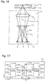
- FIG. 1 shows the brief arrangement of an optical pick-up 2 which can perform a recording/reproducing process with a thick optical disk 1a having a low recording density according to the CD standard and a thin optical disk 1b having a high recording density according to the DVD standard, and the brief arrangement of an optical recording system 17 in which the optical pick-up 2 is employed.
- the optical pick-up 2 according to this embodiment comprises an integrated device 10 in which a surface emitting laser 3 serving as a light source and a photo detector array for signal detection 4 using photo diodes serving as light detectors are monolithically formed on a single substrate (e.g., n-type GaAs substrate).
- a laser beam 7 emitted from the surface emitting laser 3 is converged on the recording layer of an optical disk 1 through a hologram 6, a polarization dependent optical element (polarizer) 9, and an objective lens 5 which constitute an optical element 15 of the optical pick-up 2 according to this embodiment, and a reflected beam 8 from the recording layer passes through the optical element 15 again to be converged on the photo detectors.
- the laser beam 7 emitted with a polarization direction determined by a laser controller 11 passes through the hologram 6, and is converged on the recording layer of the optical disk 1 by the objective lens 5.
- the reflected beam 8 reflected from the recording layer of the optical disk 1 is incident on the objective lens 5 through the same optical path as described above to be diffracted by the hologram 6, and the ⁇ 1-order beams of the diffracted reflected beam are converged on the photo detector array 4 of the integrated device 10 such that an conspicuous astigmatic aberration is generated.
- Signals obtained by the photo detector array 4 undergo an arithmetic operation by an arithmetic operation circuit 12.
- the optical pick-up 2 is positionally controlled by an actuator using electromagnetic force such that a tracking error or a focusing error is minimized.
- the surface emitting laser 3 serving as a laser beam source LD for emitting a laser beam is arranged at the center or almost the center, and photo detector arrays 4a and 4b arranged in two rows are formed on both sides of the surface emitting laser 3. Electrode pairs 32a and 32b are connected to the laser beam source LD. As will be described later, when the electrodes 32a and 32b are switched by the laser controller 11, the polarization direction of the laser beam 7 emitted from the laser beam source LD can be controlled.
- a pit recorded on an optical disk has a long and narrow shape along a track direction.
- TM-polarized light linearly polarized light perpendicular to a pit length direction, i.e., perpendicular to the track direction
- TE-polarized light linearly polarized light perpendicular to the track direction
- TM-polarized light is preferably used to perform a recording/reproducing process with the optical disk 1b having a high recording density
- TE-polarized light is preferably used for the optical disk 1a having large recording pits.
- the electrodes 32a are selected to perform a recording/reproducing process with the thick optical disk 1a having a low recording density according to the CD standard, and a TE-polarized laser beam 7a mainly having a TE-polarized light component is emitted from the laser beam source LD.
- a TM-polarized laser beam 7b mainly having a TM-polarized light component is emitted from the laser beam source LD.
- laser beams having the polarized light components opposite to the above light components can also be selected for the CD standard and the DVD standard.
- the polarizer 9 is arranged on the optical path between the laser beam source LD and the objective lens 5.
- a central portion 9a is a circular transparent portion (i.e., a portion from which a polarization separation film is removed) having high transmittance with respect to both the TE-polarized light and the TM-polarized light
- the peripheral portion 9b serves as polarization separation film in which the transmittance with respect to TE-polarized light is almost zero.
- a polarization dependent optical element can be constituted by using, e.g., an absorption type organic polarization filter.
- This filter is formed such that a polymer film containing an organic dye is extended in order to arrange the molecules of the organic dye in the same direction.
- a polarization dependent optical element can also be constituted by a polarization filter obtained by stacking films having birefringence, a polarization filter obtained by dispersing metal needles on a transparent substrate, a birefringent grating polarizer, or the like.
- the TE-polarized laser beam 7a is emitted from the laser beam source LD onto the thick optical disk 1a according to the CD standard.
- the TE-polarized laser beam 7a decreases the effective numerical aperture NA of the objective lens 5, and the effective numerical aperture NA is set to about 0.35 in this embodiment.
- the TM-polarized laser beam 7b is emitted from the laser beam source LD onto the thin optical disk 1b according to the DVD standard. Since the TM-polarized laser beam 7b almost entirely transmits through the polarizer 9, the numerical aperture NA of the objective lens 5 is equal to its design value.
- the objective lens of this embodiment is optimally designed for the thin optical disk 1b according to the DVD standard, and the objective lens is designed such that the effective numerical aperture NA is set to about 0.6 with respect to the laser beam 7 having a wavelength of about 650 nm.
- the photo detector arrays 4a and 4b are arranged in two rows on both sides of the laser beam source LD to detect the reflected beam 8.
- Four strip-shaped photo diodes 13a, 13b, 13g, and 13h and four strip-shaped photo diodes 13e, 13f, 13c, and 13d are formed on the photo detector arrays 4a and 4b, respectively, to obtain, from the reflected beam 8, a focusing error signal for performing focusing servo, a tracking error signal for performing tracking servo, and data signal for obtaining information recorded on an optical disk.
- the ⁇ 1-order lights of the reflected beam 8 divided in the tangential direction of the track of the optical disk 1 are converged on these photo diodes 13a to 13h to generate conspicuous astigmatic aberration by hologram 6. Therefore, the optical intensities of the beams are converted into signal strengths by the photo diodes 13a to 13h, and the signals are calculated by the arithmetic operation circuit 12 to be output.
- the arithmetic results of the arithmetic operation circuit 12 are transmitted to the position controller 16, and the optical pick-up 2 is positionally controlled such that a tracking error and a focusing error are minimum.
- a focusing error signal FES is obtained by arithmetic operation on the signal strengths obtained by the photo diodes 13a to 13h in the following manner: ⁇ (13a + 13b) + (13c + 13d) ⁇ - ⁇ (13g + 13h) + (13e + 13f) ⁇
- a tracking error signal TES can be calculated by a push-pull method using the difference between the optical strengths of the reflected beams in the areas separated in the tangential direction.
- the tracking error signal TES is obtained by arithmetic operation in the following manner: ⁇ (13a + 13b) + (13e + 13f) ⁇ - ⁇ (13c + 13d) + (13g + 13h) ⁇
- the tracking error signal TES can be also calculated by a differential phase tracking method using a signal strength representing the difference between light intensities of diagonal areas of the areas divided by 4 in the tangential direction and the radial direction with respect to the track of the optical disk.
- the tracking error signal TES is obtained by arithmetic operation in the following manner: ⁇ (13b + 13c) + (13e + 13h) ⁇ - ⁇ (13a + 13d) + (13f + 13g) ⁇
- a tracking error signal can be obtained regardless of the track pitch of the optical disk. Therefore, the optical pick-up 2 having compatibility with the optical disk 1b having a high recording density and the optical disk 1a having a low recording density can be realized.
- a data signal RFS can be obtained by the total sum of the photo diodes 13a to 13h.
- the data signal RFS is obtained by arithmetic operation in the following manner: (13a + 13b + 13c + 13d + 13e + 13f + 13g + 13h)
- the TM-polarized laser beam 7b is emitted from the laser beam source LD of the surface emitting laser 3 and converged on the recording layer of the optical disk 1b by the objective lens 5.
- the objective lens 5 of this embodiment is optimally designed such that light can be converged to diffraction limit on the recording layer of the thin optical disk 1b when the numerical aperture NA is 0.6. Therefore, by using the TM-polarized laser beam 7b, a laser beam emitted from the laser beam source LD almost entirely transmits through the polarizer 9 to be converged on the optical disk 1b with high focusing performance. Therefore, since the reflected beam 8 having high resolution can be obtained, the optical disk 1b according to the DVD standard can be stably positionally controlled at high precision, and a recording/reproducing process can be reliably performed.
- the TE-polarized laser beam 7a is emitted from the laser beam source LD of the surface emitting laser 3.
- the laser beam 7a is stopped down by the aperture 9a of the central portion of the polarizer 9 to be incident on the objective lens 5. Therefore, for the objective lens 5 of this embodiment, the optical system of an optical pick-up is designed such that the effective numerical aperture NA is set to 0.35 with respect to the TE-polarized laser beam 7a.
- the objective lens 5 is optimally designed for a thin optical disk having a substrate thickness of 0.6 mm and a high recording density
- a spherical aberration is generated, and imaging performance is degraded.
- an effective numerical aperture NA is set to a small value of 0.35 with respect to the thick optical disk 1a having a low recording density.
- a spherical aberration generated by the difference between substrate thicknesses is in proportion to the 4th power of the numerical aperture NA. Therefore, when the numerical aperture is decreased, a spherical aberration sharply decreases even if the substrate thickness are different from each other.
- the optical pick-up 2 of this embodiment can form a convergent spot obtained by converging the TE-polarized laser beam 7a to almost diffraction limit on the thick optical disk 1a having a substrate thickness of 1.2 mm, and an influence of the error of the substrate thickness on an spherical aberration can be considerably decreased.
- the diameter of the convergent spot is increased by a decrease in the numerical aperture.
- the information recording density of the thick optical disk 1a is lower than that of the thin optical disk 1b, such diameter is sufficiently small as the diameter of the convergent spot.
- FIG. 3(a) shows a manner in which, when a beam (TE-polarized laser beam) for reproducing a CD is incident on the objective lens 5 to change the diameter of the transparent portion 9a of the polarizer 9 thereby to change the effective numerical aperture, the diameter of a convergent spot formed by the objective lens 5 onto the recording surface of the CD 1a changes.
- FIG. 3(b) shows a manner in which the wave aberration of the convergent spot changes depending on the change in diameter.
- the convergent spot diameter is set to a diameter at which the strength of the main lobe of the convergent spot is set to 1/e 2 of the peak value.
- FIG. 3(a) shows a manner in which the convergent spot diameter changes as a function of the rate of aperture limit (aperture reduction rate) by the polarizer 9 plotted on the abscissa.
- the aperture reduction rate is increased to decrease the effective numerical aperture
- the convergent spot diameter decreases as shown in FIG. 3(a)
- the wave aberration increases as shown in FIG. 3(b).
- a wave aberration in an optical pick-up is generally regulated to 0.071 ⁇ or less with the wavelength ⁇ as rms (root mean square) average by the Marecial Criterion.
- the allowed wave aberration about 0.05 ⁇ is allowed as a wave aberration generated by the substrate of a CD.
- the wave aberration of the optical system of the optical pick-up must be set to 0.05 ⁇ or less. Therefore, with reference to the measurement result in FIG. 3(b), in order to satisfy this condition, the aperture reduction rate is desirably set to about 64% or less.
- FIG. 3(c) shows a result obtained by measuring a jitter value of a 3T signal serving as a shortest pit when the CD 1a is reproduced while an aperture reduction rate is changed.
- the jitter value a value obtained by standardizing the value of the standard deviation of a distribution by an window width is set.
- a jitter value at which a BER (Bit Error Rate) of 10 -5 or less is obtained is 15%.
- the aperture reduction rate is preferably set to about 50% or more.
- the aperture reduction rate by the polarizer 9 is preferably set to about 50 to 64%.
- the aperture reduction rate is more preferably set to about 56% to 60%. According to these results, in the optical pick-up of this embodiment, about 58% is employed as the reduction rate of the numerical aperture of the polarizer 9, and the numerical aperture of 0.6 set for a DVD is stopped down to 0.35 for a CD.
- the optical pick-up 2 of this embodiment is an optical pick-up having high compatibility with the high-recording-density optical disk 1b and the low-recording-density optical disk 1a which are different from each other in thickness, track pitch, and the like.
- the optical pick-up 2 can cope with the optical disks 1a and 1b by changing the polarization direction of the laser beam, the optical pick-up 2 is realized as an inexpensive and compact optical pick-up in which a simple optical system having high reliability is employed. Control for the polarization direction of a laser beam can be performed by only switching electrodes of the surface emitting laser 3 connected to the laser beam source LD. This control can be achieved by an extremely simple controller and has high reliability.
- a plurality of conventional edge emitting laser diodes may be prepared and arranged in different directions to make it possible to obtain the light source.
- the positional relationship between the irradiation positions of the plurality of semiconductor chips and a photo detector array for detecting reflected laser beams must be adjusted.
- the optical pick-up 2 of this embodiment employs the surface emitting laser 3 as a laser beam source as described above.
- a plurality of laser beam sources are two-dimensionally arranged to be integrated as a matter of course, and a laser beam is irradiated perpendicularly to the substrate plane on which a VCSEL is formed but from the edge. For this reason, as described above, it is easy to monolithically arrange the laser beam sources and light detectors such as photo diodes on a single substrate.
- the vertical cavity surface emitting laser in which resonant paths are formed perpendicularly to the substrate and constitute a two-dimensional array, the degrees of density and in-plane arrangement are high.
- the vertical cavity surface emitting laser is one of light sources which are most suitable for the optical pick-up according to the present invention.
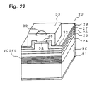
- FIG. 4 shows the outline of a VCSEL
- FIG. 5 shows an arrangement of the VCSEL by using the cross sectional view of the VCSEL
- FIG. 6 shows the appearance of the VCSEL of this embodiment when viewed from the emitting side of a laser beam.
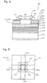
- the VCSEL of this embodiment comprises an optical resonator 20 in which a plurality of semiconductor layers are stacked between metal layers 21 and 32.
- an n-type GaAs buffer layer 23 60 pairs of semiconductor distributed Bragg reflectors 24 each constituted by an n-type AlAs layer and an n-type Al 0.5 Ga 0.5 As layer and together having a reflectance of 99% or more with respect to light having a wavelength of about 650 nm, an n-type Al 0.7 Ga 0.3 As clad layer 25, a multi-quantum well active layer 26 constituted by five n - -type Ga 0.5 In 0.5 P well layers and n - -type (Al 0.5 Ga 0.5 ) 0.5 In 0.5 P barrier layers, a p-type Al 0.7 Ga 0.3 As clad layer 27, and a p-type Al 0.2 Ga 0.8 As contact layer 28 are sequentially stacked on an n-type GaAs substrate 22 from the bottom.
- Epitaxial growth using the MOVPE method or epitaxial growth using the MBE method can be used to form these stacked layers.
- 8 pairs of dielectric multilayer reflectors 33 each constituted by a first layer, e.g., an SiO x layer such as SiO 2 and a second layer, e.g., a TaO x layer such as Ta 2 O 5 and having a reflectance of 98.5% or more with respect to light having a wavelength of about 650 nm are formed on the area which sufficiently covers an exposed surface 35 (referred to as an aperture hereinafter) of the contact layer 28 on the emitting side.
- the contact layer 28 and a part of the clad layer 27 are etched into a square or almost square shape when viewed from the upper surface of the resonator 20, i.e., the emitting side to form a column 34, and this column 34 serves as a resonant portion.
- the lateral cross section of the column 34 parallel to the substrate 22 is formed into a square or almost square shape, the direction of the polarization direction of a laser beam emitted from the oscillation area of the column 34 is along one of two orthogonal sides of the square.
- the periphery of the column 34 is buried with a first insulative layer 29 constituted by a silicon oxide film (SiO x film) such as an SiO 2 film formed by a thermal CVD method and a metal layer 30 consisting of a metal such as a gold-zinc alloy.
- the first insulative layer 29 is continuously formed along the p-type Al 0.5 Ga 0.5 As clad layer 27 and the surface of the contact layer 28, and the metal layer 30 is formed to bury a portion around the first insulative layer 29.
- a second insulative layer 31 constituted by a silicon oxide film (SiO x film) such as an SiO 2 film formed by a spattering method is formed on the surface of the metal layer 30, the metal layer (upper electrode) 32 consisting of, e.g., Cr and a gold-zinc alloy is formed on the second insulative layer 31 to be in contact with the contact layer 28, and the contact metal layer 32 serves as an electrode for current injection.
- the upper electrode 32 is divided by 4 into two pairs of electrodes 32a and 32b, and the pairs of electrodes 32a and 32b are formed to be in contact with the respective sides of the column 34 as shown in FIG. 6.
- the interior of the upper electrode 32 serves as the aperture 35.
- a current is injected from the upper electrode 32, the current is guided to the active layer 26 to be converted into light, and the light is amplified by the resonator, and the laser beam is emitted from the aperture 35 to the outside.
- the VCSEL having one column 34 is shown.
- a plurality of columns may be arranged in the surface of the substrate, as a matter of course.
- a plurality of optical resonators 20 each having the above arrangement can also be easily combined to each other in the form of an array to be integrated.
- TE-polarized and TM-polarized laser beams can be selectively emitted from the VCSEL by switching the pairs of upper electrodes 32a and 32b.
- a manner of emitting laser beams having different polarization directions will be described below with reference to FIG. 6.
- FIG. 6 is a schematic view showing the VCSEL of this embodiment when viewed from a side on which a laser beam is emitted.
- the upper electrode 32 is formed along the respective sides of the contact layer 28 having a square shape.
- Each pair of opposite parts of the upper electrode 32 serves as a pair of electrodes 32a and 32b, respectively.
- a current from two sides of the square contacting the pair of upper electrodes 32a is guided to the active layer 26 while being dispersed toward the central portion of the square, thereby performing laser oscillation.
- the lateral cross section of the column 34 is square, and the pairs of upper electrodes 32a and 32b are symmetrically formed. Therefore, there are no differences in the characteristics of the VCSEL such as threshold current, wallplug efficiency, and the like which are performed when the VCSEL is driven by using only the pair of upper electrodes 32a or the pair of upper electrodes 32b.
- an influence on the distribution of electric field near an interface at the inside and periphery of the column 34 as a part of the optical resonator 20 in use of only the pair of upper electrodes 32a is different from that in use of only the pair of upper electrodes 32b. More specifically, when the VCSEL is not driven, due to the metal layer 30 formed around the column 34, the distributions of electric field around the column 34 are equal to each other with respect to the respective sides of the square, the polarization direction of a laser beam which can exist inside the column 34 is along one of orthogonal sides and cannot be controlled.
- the polarization direction of light transmitted through the inside of the column 34 is equal to a direction perpendicular to the sides of the square contacting the pair of upper electrodes 32a.
- the polarization direction of an emitter laser beam has a direction in which an electric field easily exists, i.e., the direction of the pair of upper electrodes 32a, and the TE-polarized laser beam 7a is emitted.
- the polarization direction of a laser beam emitted when a current is injected into the VCSEL by using the pair of upper electrodes 32b has a direction perpendicular to the direction of the laser beam (TE-polarized light) obtained by using the pair of upper electrodes 32a, i.e., to be TM-polarized light because the sides of the square contacting the pair of upper electrodes 32b are perpendicular to the sides contacting the pair of upper electrodes 32a.
- the polarization direction of an emitted laser beam can be controlled, and TE-polarized or TM-polarized laser beams can be selectively emitted.
- the laser beams form orthogonal polarization directions. For this reason, laser oscillations can be stably performed.
- a laser beam source which can selectively irradiate laser beams having different polarization directions is realized by using a vertical cavity surface emitting laser.
- the optical element 15 comprises a polarizer 9 having an aperture formed therein, and polarizer 9 is arranged between the laser beam source 3 and the objective lens 5. For this reason, only by selecting the electrodes of the surface emitting laser diode to change the polarization direction of a laser beam, the effective numerical aperture NA of the objective lens 5 is controlled for optical disks having different thickness, and the numerical aperture of the optical element 15 can be changed. Therefore, a beam spot having high resolution can be converged on any optical disks having different thickness.
- the servo function of the optical pick-up can be utilized, and a recording/reproducing process can be reliably performed with optical disks having different thickness. Therefore, a data process can be reliably performed with a plurality of optical disks having different recording densities.
- the optical pick-up of this embodiment laser beams having different polarization directions are selectively irradiated on optical disks having different thickness and different track pitches to obtain a reflected beam having high resolution.
- the optical pick-up does not require a process of splitting one laser beam into a plurality of focusing points to be converged as with conventional pick-ups, and a simple optical system having high reliability can be applied to the optical pick-up. Since the optical pick-up does not require an optical element such as a prism or a hologram for splitting a laser beam, the optical pick-up having compatibility with optical disks having different thickness can be decreased in size and weight.
- the optical pick-up of this embodiment employs, as a light source, a new vertical cavity surface emitting laser in which can switch a polarization direction and can be easily integrated, the optical pick-up can be more decreased in size, and has a considerably simple structure and high performance.
- the optical pick-up of this embodiment does not split a laser beam into two beams to converge two focusing points as the conventional pick-up, when a TM-polarized laser beam is irradiated on a thin optical disk, a laser power can be prevented from being decreased, and a decrease in laser power of TE-polarized light can be prevented except for only a decrease in laser power caused by absorption or diffraction by a polarization separation film.
- a switching operation of polarization directions can be reliably performed by very simple control such as selection of pairs of electrodes as described above. Therefore, an optical pick-up which can cope with optical disks having a plurality of specifications can be provided with an inexpensive arrangement having high reliability.
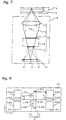
- FIG. 7 shows the second embodiment of an optical pick-up 2 which can perform a recording/reproducing process with a thick optical disk 1a having a low recording density according to the CD standard and a thin optical disk 1b having a high recording density according to the DVD standard.
- the optical pick-up 2 according to this embodiment comprises an integrated device 10 in which surface emitting lasers 3 serving as light sources are arrayed to form a plurality of laser beam sources, the surface emitting laser array 3 and a photo detector array 4 for signal detection using photo diodes serving as light detectors are monolithically formed on a single substrate.
- a laser beam 7 emitted from the surface emitting laser array 3 is converged by an objective lens 5 on the recording layer of an optical disk 1 through a hologram 6 of an optical element 15.
- a reflected beam 8 reflected from the recording layer of the optical disk 1 is incident on the objective lens 5 of the optical element 15 through the same optical path as described above and diffracted by the hologram 6, and ⁇ 1-order beams of the diffracted reflected beam are converged on the photo detector array 4 of the integrated device 10 such that a conspicuous astigmatic aberration is generated. Therefore, the optical recording system shown in FIG. 1 can also be provided by using the optical pick-up 2 of this embodiment. A description of the arrangement of the optical recording system will be omitted. As in the first embodiment, since a surface emitting laser is used in the second embodiment, the sectional shape of the emitted beam is almost circular.
- a prism or lens for shaping a beam is not required, and the optical system can be simplified.
- the beam shaping prism is not required, a factor that generates an aberration and a factor that increases production cost can be removed, and the compact, light-weight, and inexpensive optical element 15 having high precision can be employed.
- the hologram 6 is formed on one surface of a hologram element 19, and a polarized hologram 18 having refractive power is formed on the other surface of the hologram element 19. Therefore, the optical element of this embodiment comprises the hologram 6, the polarized hologram 18 having refractive power, and the objective lens 5.
- the polarized hologram 18 of this embodiment a polarized Fresnel-zone plate having positive power to a TE-polarized laser beam is formed.
- the polarized hologram 18 of this embodiment when a TE-polarized laser beam 7a is irradiated from the laser beam source 3, the TE-polarized laser beam 7a passes through the polarized hologram 18 such that a radiation angle decreases.
- the polarized hologram 18 has no power to a TM-polarized laser beam 7b.
- Power of the polarized hologram 18 of this embodiment with respect to the TE-polarized laser beam is selected such that a reduction rate of the effective numerical aperture NA of the objective lens 5 is set to about 58% as in the above embodiment.
- the aperture reduction rate of the polarized hologram 18 of the optical pick-up 2 according to this embodiment is preferably set to about 50 to 64% as in the polarizer 9 of the optical pick-up described above, more preferably set to about 56% to 60%.
- FIG. 8 is an enlarged view showing a plane arrangement of the integrated device 10 of this embodiment.
- the integrated device 10 of the embodiment comprises a surface emitting laser array 3 in which a plurality of laser beam sources LD for emitting laser beams are formed in two rows in the center or almost the center of the integrated device 10.
- a first laser beam source group 3a on the right in the drawing of the surface emitting laser array 3 is a laser beam source group for performing a recording/reproducing process with the optical disk 1a having a thick substrate and a low recording density according to the CD standard.
- a second laser beam source group 3b arranged parallel to the first laser beam source group 3a is a laser beam source group for performing a recording/reproducing process with the optical disk 1b having a thin optical disk and a high recording density according to the DVD standard.
- Three laser beam sources LD1b, LD2b, and LD3b constituting the second laser beam source group 3b are arranged at a pitch L2 corresponding to the track pitch (0.74 ⁇ m) of the optical disk 1b according to DVD standard. Therefore, a ratio of pitches L1 : L2 is almost equal to 1.6 : 0.74.
- the three laser beam sources LD1a, LD2a, and LD3a constituting the first laser beam source group 3a are arranged such that a TE-polarized laser beam having a wavelength of about 650 nm can be irradiated.
- the radiation angle of the emitted laser beam is decreased by the above polarized hologram 18, so that the effective numerical aperture NA of the objective lens 5 is set to about 0.35.
- the laser beam sources LD1b, LD2b, and LD3b constituting the second laser beam source group 3b are arranged such that a TM-polarized laser beam having a wavelength of about 650 nm can be irradiated. Since the TM-polarized light passes through the polarized hologram 18, the effective numerical aperture NA of the objective lens 5 is set to about 0.6.
- first and second laser beam source groups 3a and 3b On both sides of the first and second laser beam source groups 3a and 3b, two rows of photo detector groups 4a and 4b for detecting reflected beams are arranged parallel to the first and second laser beam source groups 3a and 3b. Three photo diodes PD1a, PD2a, and PD3a and three photo diodes PD1b, PD2b, and PD3b are arranged in the photo detector groups 4a and 4b such that a tracking error signal is obtained by the three-beams method in correspondence with laser beam sources LD1 to LD3.
- the surface emitting laser arrays and the diode groups described above can be formed at high precision in a fine space by a photolithographic technique.
- the surface emitting laser arrays and the diode groups can be formed on a single integrated device 10 and then provided.
- a focusing error signal FES can be obtained by the difference between the intensities of ⁇ 1-order light of the reflected beams 8 which are converged on the first photo detector array 4a and the second photo detector array 4b such that a conspicuous astigmatic aberration is generated by the hologram 6.
- a data signal RFS representing data recorded on the optical disk 1a or 1b can be calculated on the basis of the intensity of the reflected beam 8.
- the second laser beam source group 3b of the surface emitting laser array 3 is selected, and laser beams 7b are irradiated from the three laser beam sources LD1b, LD2b, and LD3b constituting the second laser beam source group 3b.
- the central laser beam source LD2b of these laser beam sources serves as a main beam source for outputting a data signal and a focusing error signal by an astigmatic aberration method, and the laser beam sources LD1b and LD3b arranged on both sides of the laser beam source LD2b serve as sub-beam sources for outputting tracking error signals by the three-beams method.
- the laser beams 7b emitted from the laser beam sources LD1b, LD2b, and LD3b are converged on the recording layer of the optical disk 1b by the objective lens 5.
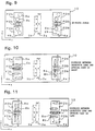
- FIGS. 9, 10, and 11 show a manner in which reflected beams 8b reflected from the optical disk 1b are converged on the photo detector arrays 4a and 4b in an in-focus state, a state wherein the objective lens 5 and the optical disk 1b are close to each other, and a state wherein the objective lens 5 and the optical disk 1b are far from each other, respectively.
- signal strengths obtained from the photo detectors PD2a and PD2b on which ⁇ 1-order beams are converged are substantially equal in the in-focus state shown in FIG. 9.
- the focal points are offset from each other, as shown in FIG. 10 or 11, the signal strengths obtained from the photo detectors PD2a and PD2b are different.
- a convergent state is obtained as a focusing error signal FES, and a focusing servo operation is performed on the basis of this signal, and the servo operation can be reliably performed.
- FES focusing error signal
- a tracking error occurs, signal strengths obtained from the photo diodes PD1a, PD1b, PD3a, and PD3b for detecting the sub-beams are different. For this reason, this state is obtained as the tracking error signal TES, and a tracking servo operation can be performed on the basis of this signal.
- the hologram 6 pattern-designed in the following manner is used. That is, a main beam and sub-beams reflected from the optical disk 1a or 1b are diffracted to ⁇ 1-order diffraction, and the optical axes of these beams are changed to generate a conspicuous astigmatic aberration.
- a pattern along a hyperbola group or a corrected hyperbola group is used as the pattern of a grating, and the grating is arranged such that ⁇ 1-order diffracted light is parallel to the longitudinal direction (x axis) of the device 10. Therefore, when the objective lens 5 is close to the optical disk 1a or 1b, as shown in FIG.
- the spot of + 1-order diffracted light converged on the photo diodes PD1a, PD2a, and PD3a has an elliptical shape having a major axis parallel to the x axis
- the spot of -1-order diffracted light converged on the photo diodes PD1b, PD2b, and PD3b has an elliptical shape having a major axis parallel to the y axis.
- the objective lens 5 and the disk 1a or 1b are far from each other, as shown in FIG.
- the spot of + 1-order diffracted light has an elliptical shape having a major axis parallel to the y axis
- the spot of - 1-order diffracted light has an elliptical shape having a major axis parallel to the x axis. Therefore, as described above, amounts of light received by the photo diodes PD2a and PD2b change, and the focusing error signal FES can be obtained.
- the photo diodes PD2a and PD2b formed on the device 10 of this embodiment are arranged on the same straight line as that of the laser beam sources LD2a and LD2b to form a rectangle having long sides parallel to the straight line.
- the length of the long side of the rectangle is sufficiently longer than the interval between the laser beam sources LD2a and LD2b. Therefore, when the thick optical disk 1a is to be reproduced, or when the thin optical disk 1b is to be reproduced, a focusing error signal can be detected by common photo detectors.
- the wavelength of a beam emitted from the surface emitting laser array 3 or the distance between the surface emitting laser array 3 and the hologram 6 on the optical axis is subject to tolerances, the spots of ⁇ 1-order diffracted lights converged on the photo diodes PD2a and PD2b only move on the x axis. For this reason, the spots can be reliably caught. Therefore, as in the device 10, when the photo diodes PD2a and PD2b are arranged in a rectangle having long sides parallel to the x axis, the precision of the wavelength of a light source, the assembly precision of the light source, and the like can be moderated. This is advantageous to manufacturing an optical pick-up.
- the photo detection areas of the photo diodes PD1a, PD3a, PD1b, and PD3b for detecting a tracking error signal are sufficiently large.
- Each photo detection area has a square or almost square shape having a side whose length is equal to the length of the long side of the photo diode PD2a or PD2b. Therefore, as in detection for a focusing error signal, the photo diodes PD1a, PD3a, PD1b, and PD3b can be used to detect the tracking error signals from both the thick optical disk (disk according to the CD standard) 1a and the thin optical disk (disk according to the DVD standard) 1b.
- the precision of the wavelength of the laser beam source and the assembly precision of the laser source can be also moderated.
- the laser beam sources LD1b, LD2b, and LD3b are arranged in the surface emitting laser array 3b of this embodiment at intervals corresponding to the track pitch of an optical disk having a high recording density.
- the objective lens 5 of this embodiment is optimally designed such that the effective numerical aperture NA is set to 0.6 for the laser beam 7b emitted at a predetermined radiation angle from the second laser beam source group 3b, and the laser beam 7b can be converged to diffraction limit on the recording layer of the thin optical disk 1b.
- the laser beam 7b emitted from the second laser beam source group 3b is converged on the recording layer to obtain a reflected beam having high resolution, a conspicuous tracking error signal TES is obtained, and a tracking servo operation can be reliably performed. For this reason, positional control can be stably performed at high precision with the thin optical disk 1b having a high recording density, and a recording/reproducing process can be reliably performed.
- the first laser beam source group 3a of the surface emitting laser array is selected, and laser beams 7a are irradiated from the three laser beam sources LD1a, LD2a, and LD3a constituting the first laser beam source group 3a.
- the central laser beam source LD2a of these laser beam sources serves as a main beam source for outputting a data signal and a focusing error signal by an astigmatic aberration method
- the laser beam sources LD1a and LD3a arranged on both sides of the laser beam source LD2a serve as sub-beam sources for outputting tracking error signals by a three-beams method.
- the laser beams 7b emitted from the laser beam source group are converged on the recording layer of the optical disk 1b by the objective lens 5.
- a reflected beam 8a reflected from the optical disk 1a according to the CD standard is converged like the reflected beam 8b as indicated by the broken lines in FIGs. 9, 10, and 11, and a data signal and a focusing error signal can be obtained.
- the laser beam sources LD1a, LD2a, and LD3a are arranged at a pitch corresponding to the optical disk 1a having a large track pitch and a low recording density. For this reason, a tracking error signal can also be obtained by the three-beams method with respect to the optical disk 1a.
- the objective lens 5 of this embodiment is designed such that the effective numerical aperture NA is set to about 0.35 when the radiation angle of TE-polarized light emitted from the first laser beam source group 3a is decreased. Therefore, although the objective lens 5 is optimally designed for a thin optical disk having a substrate thickness of 0.6 mm and a high recording density, the numerical aperture of the optical element 15 is decreased for a thick optical disk having a substrate thickness of 1.2 mm and a low recording density so that the laser beam 7a can be converged to almost diffraction limit, and a focusing operation and a tracking servo operation can be performed with the optical disk 1a having a large track pitch and a low recording density by using the same control system as that used for the optical disk 1b having a small track pitch and a high recording density.
- the radiation angle of the laser beam 7a is decreased by the polarized hologram 18, so that the effective numerical aperture NA of the objective lens 5 can be decreased. For this reason, a spherical aberration by a substrate thickness is suppressed from being generated, and the reflected beam 7a having high resolution can be obtained. Therefore, a recording/reproducing process can be performed with the optical disk having a low recording density.
- the optical pick-up 2 of this embodiment is also an optical pick-up having compatibility with the high-recording-density optical disk 1b and the low-recording-density optical disk 1a which are different from each other in thickness and track pitch.
- the optical pick-up 2 of this embodiment only selects the first or second laser beam source 3a or 3b on the basis of a selection signal from a laser controller 11 in the optical recording system shown in FIG. 1 to change the polarization direction of a laser beam irradiated on an optical disk, the optical pick-up 2 can cope with the optical disks 1a and 1b.
- the optical system which can be prevented from being complicated and has high reliability can be employed, and an inexpensive and compact optical pick-up having high performance can be provided.
- the optical pick-up of this embodiment since laser power is not divided, a recording/reproducing process can be performed with low power consumption.
- the surface emitting laser array in which a plurality of laser beam sources can be formed in a small area by using the photolithographic technique, a plurality of laser beam sources corresponding to the track pitches of the respective optical disks 1a and 1b can be formed, so that an optical pick-up which can obtain tracking error signals by using a three-beams method with respect to the optical disks 1a and 1b and has a very small size and a simple arrangement is realized.
- the three-beams method a stable tracking error signal can be obtained, and a simple control system can be used. For this reason, the three-beams method is used in many optical pick-ups for CD.
- the three-beams method can be applied to the different types of optical disks, and tracking and focusing control can be performed by a single control system.
- the surface emitting laser array 3 is employed, a total of six laser beam sources constituting the two groups of laser beam sources 3a and 3b can be arranged in a very small space.
- the laser beam sources for outputting a main beam and sub-beams are separated from each other, a laser beam for detecting an information signal and a focusing error signal and a laser beams for detecting a tracking error signal can be emitted at different timings.
- the flow of processes is executed in the following rough order. That is, the optical disk is determined, the surface emitting lasers corresponding to the optical disk are turned on, focus drawing and focusing control are performed, tracking control is performed, laser beams are moved to a desired address, and an information signal is reproduced.
- the arithmetically calculated tracking error and focusing error signals are supplied to, e.g., a position controller 13 shown in FIG. 1, the optical pick-up 2 is moved by an actuator in a direction perpendicular to the recording surface of the optical disk or a radial direction of the optical disk, and control for converging a laser beam to a target pit on the recording track of the optical disk to form a fine spot is performed.
- the convergent spots of sub-beams are arranged in front of and behind the convergent spot of a main beam in the track direction. For this reason, since a time difference is generated between the signals of the two sub-beams, abnormality of a tracking error signal may occur when the beam spots pass through cracks or defects on the disk.
- the interval between the convergent spots of the main beam and the sub-beam is preferably set to 15 ⁇ m or less.
- the pitches L1 and L2 of the laser beam sources decrease.
- the pitch L2 of the laser beam sources 3b corresponding the optical disk 1b according to the DVD standard considerably decreases.
- the range in which two adjacent emitting portions of the surface emitting laser array 3 can be closest to each other is determined by the cross sectional shapes of the columns constituting the optical resonators of the emitting portions parallel to the semiconductor substrate. Since the size of a general cross section is 10 to 30 ⁇ m, the minimum interval between the adjacent laser beam sources, i.e., the pitch L2 of the laser beam sources 3b is preferably set to 30 ⁇ m or more.
- a magnification m of the optical element 15 of this embodiment is a ratio (f1/f2) of an optical length f1 between an object surface (light source) and an object side principle point (after the optical elements such as the objective lens 5 and the polarized hologram 18 constituting the optical element 15 are combined to each other) of the optical element 15 and an optical length f2 of an image (optical disk 1) side principal point of the optical element 15.
- the pitch L2 of the second laser beam source group 3b is given by: 15 x m x (L2/L1) ⁇ 30 ⁇ m, i.e., m x (L2/L1) ⁇ 2
- the pitch ratio L2/L1 is given by 0.74/1.6. Therefore, it is understood that as an optical element for an optical pick-up having compatibility with both the DVD standard and the CD standard, an optical system having a magnification m of 4.4 or more is desirably used.
- the minimum interval between laser beam sources is more preferably set to about 40 ⁇ m or more.
- the magnification m of the optical system satisfies the following relationship: 15 x m x (L2/L1) ⁇ 40 ⁇ m, i.e., m x (L2/L1) ⁇ 8/3
- an optical element for an optical pick-up having compatibility with both the DVD standard and the CD standard an optical element having a magnitude m of 5.8 or more is more preferably used.
- the magnification m of the optical element 15 can be replaced with the magnification of the objective lens 5, because the influence of the optical elements such as polarized hologram 18 constituting the optical element 15 except for the objective lens 5 can be almost neglected.
- an objective lens which has a numerical aperture of 0.6 and a finite system having a magnification m of 6 and is optimally designed for DVD can be used.
- the surface emitting laser array 3 in which the pitch L1 of the first laser beam source group 3a for CD is 90 ⁇ m and the pitch L2 of the second laser beam source group 3b for DVD is 41.6 ⁇ m can be applied to the objective lens 5.
- an optical pick-up having such preferable optical performance that the interval between the convergent spots of a main beam and a sub-beam for CD obtained by the objective lens 5 is set to 15 ⁇ m and the interval between the convergent spots of a main beam and a sub-beam for DVD is set to 6.9 ⁇ m.
- the interval e.g., the distance between the laser beam sources LD2a and LD2b
- the interval between the first laser beam source group 3a and the second laser beam source group 3b is set to 40 ⁇ m.
- the objective lens 5 employed in the optical pick-up 2 of this embodiment is designed such that an aberration can be corrected to an image height of ⁇ 50 ⁇ m to make it possible to moderate manufacturing precision or assembling precision. Since the magnification m of the objective lens 5 of this embodiment is 6, the objective lens 5 can allow the light source to be offset from the optical axis by a maximum of ⁇ 300 ⁇ m.
- the intermediate point obtained by connecting the laser beam sources LD2a and LD2b located at the centers of the first and second laser beam source groups 3a and 3b is defined as an optical axis, although it is considered that the laser beam source LD1a or LD3a which is maximally offset from the optical axis by 93 ⁇ m, laser beams emitted from all the light sources of all the first and second laser beam source groups can be converged by the objective lens 5 of this embodiment on the recording surface of a CD or DVD to almost diffraction limit.
- a plurality of laser beam sources must be arranged to use the three-beams method to process disks having different specifications, and the surface emitting laser described above is optimally selected.
- the degrees density and in-plane arrangement are high.
- the VCSEL may be most suitable for the optical pick-up 2 of this embodiment.
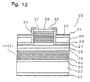
- FIG. 12 shows the arrangement of the VCSEL of this embodiment by using its cross sectional view.
- the VCSEL of the embodiment is different from the VCSEL shown in FIG. 5 in that both reflective mirrors for forming an optical resonator 20 are constituted by semiconductor Bragg reflectors, while the remaining arrangement of the VCSEL of the embodiment is that of the VCSEL in FIG. 5.
- an n-type GaAs buffer layer 23 60 pairs of semiconductor distributed Bragg reflectors 24 each constituted by an n-type AlAs layer and an n-type Al 0.5 Ga 0.5 As layer and having a reflectance of 99% or more with respect to light having a wavelength of about 650 nm, an n-type Al 0.7 Ga 0.3 As clad layer 25, a multi-quantum well active layer 26 constituted by five n - -type Ga 0.5 In 0.5 P well layers and n - -type (Al 0.5 Ga 0.5 ) 0.5 In 0.5 P barrier layers, a p-type Al 0.7 Ga 0.3 As clad layer 27, 50 pairs of semiconductor distributed Bragg reflectors 37 each constituted by a p-type AlAs layer and a p-type Al 0.5 Ga 0.5 As layer and having a reflectance of 98.5% or more with respect to light having a wavelength of about 650 nm, and a p-type
- the contact layer 28, the semiconductor distributed Bragg reflectors 37, and a part of the clad layer 27 are etched into a rectangular or almost rectangular shape when viewed from the upper surface of the resonator 20, i.e., the emitting side to form a column 34, and this column 34 serves as a resonant portion.
- this column 34 serves as a resonant portion.
- the polarization direction of an emitted laser beam can be freely set in accordance with the specification of the optical disk to be processed.
- a laser beam irradiated from an edge emitting laser diode is a light flux having an elliptical cross section.
- the optical system need not be adjusted even if the polarization direction changes.
- pairs of electrodes 32a and 32b which are separately connected to the contact layer can also be used.
- This example is shown in FIG. 14.
- the column 34 is etched into a square shape when viewed from the emitting side of the laser beam, the pairs of upper electrodes 32a and 32b are formed along the respective sides of the contact layer 28.
- a metal layer 30 is formed around the column 34. For this reason, the distributions of electric field around the column 34 are equal to each other with respect to the sides of the square.
- the distance between the active layer 26 and the upper electrodes 32 is longer than that in the structure described in the first embodiment. Therefore, in the structure of this embodiment, when a method of influencing the distribution of electric field around the column 34 shown in the first embodiment to control the polarization direction is employed, the electric field given by the upper electrodes 32 is not easily transmitted through the periphery of the column immediately above the active layer 26.
- the material of the upper electrodes 32 is selected and the contact resistance between the upper electrodes 32 and the contact layer 28 is increased. When the contact resistance is increased, and a current is caused to flow in the upper electrodes 32, portions where the upper electrodes 32 are in contact with the contact layer 28 can be slightly increased in temperature.
- the contact portions of the upper electrodes 32a have a temperature slightly higher than that of the contact portions of the upper electrodes 32b.
- the column 34 is slightly distorted by the temperature difference, the square shape is changed into a rectangular shape extending in the directions of the sides contacting the upper electrodes 32a.
- the boundary condition of the distribution of electric field around the column 34 changes, and an electric field in a direction perpendicular to the sides of the square contacting the upper electrodes 32b easily exists inside the column 34.
- the polarization direction of light transmitted through the inside of the column 34 is equal to the direction perpendicular to the sides of the square contacting the upper electrodes 32b, and the polarization direction of a laser beam to be emitted has a direction in which the electric field easily exists.
- a current is injected into the surface emitting laser diode by using the upper electrodes 32b, the polarization direction of a laser beam to be emitted is perpendicular to the direction of the polarization direction of the laser beam obtained by using the upper electrodes 32a because the sides of the square contacting the upper electrodes 32b are perpendicular to the sides of the square contacting the upper electrodes 32a.
- the laser beam sources LD1a, LD2a, and LD3a constituting the first laser beam source group 3a for emitting TE-polarized light as shown in FIG. 14(a), a surface emitting laser using the pair of upper electrodes 32a can be employed.
- a surface emitting laser using the pair of upper electrodes 32b as shown in FIG. 14(b), a surface emitting laser using the pair of upper electrodes 32b can be employed.
- the first and second laser beam source groups 3a and 3b can be constituted by using laser beam sources LD having different polarization directions, and the polarization direction of a laser beam to be emitted can be freely set depending on the specification of the optical disk to be processed.
- the laser beam sources obtained by the surface emitting laser diodes as described above there are no differences in the characteristics of the VCSEL such as threshold current, wallplug efficiency, and the like when the VCSEL is driven by using only the pair of upper electrodes 32a or the pair of upper electrodes 32b.
- a surface emitting laser array having an advantage that laser beam sources which can selectively irradiate laser beams having different polarization directions can be arrayed at high precision by the photolithographic technique is used. For this reason, a plurality of laser beam sources can be arranged in a small space in an optical pick-up, and the effective numerical aperture NA of the optical element of the optical pick-up can be controlled with respect to optical disks having different thickness without changing the arrangement of the optical pick-up which copes with a single type of optical disk. Therefore, a beam spot can be converged on any one of optical disks having different thickness, and a reflected beam having high resolution can be obtained.
- a recording/reproducing process can be reliably performed with optical disks having different thickness.
- a plurality of laser beam sources are arranged in a surface emitting laser array at a pitch corresponding to the track pitch of each optical disk, and a tracking servo operation can be performed with optical disks having different track pitches by the three-beams method which can be reliably performed and can be easily controlled. Therefore, a data process can be more reliably performed with a plurality of optical disks having different recording densities.
- the optical pick-up of this embodiment is a compact and light-weight optical pick-up in which a process of splitting a laser beam need not be performed with optical disks having different thickness and different track pitches, an inexpensive and highly reliable optical system can be applied, and reliable control coping with optical disks having different specifications can be performed.
- the optical pick-up of this embodiment is inexpensive and highly reliable, and can be expected to perform a reliable operation which rarely generates a write error or a read error for the optical disks having a plurality of specifications.
- the optical pick-up has high compatibility with various types of optical recording media for various applications which will coexist in the future, and is suitable for an optical recording system which can process all of these optical disks.
- an objective lens which is optimally designed for the thick optical disk 1a having a low recording density can be used as a matter of course.
- a polarized hologram a hologram designed such that the total numerical aperture of the objective lens and the polarized hologram is 0.6 for the optical disk 1b when the TM-polarized laser beam 7b is used and a converging operation can be performed to diffraction limit may be used.
- the value of the effective numerical aperture NA described above is only an example.
- the effective numerical aperture NA is not limited to the above value, and the values of the specifications of the optical elements including an objective lens and the specification of the laser beam sources can be set to values suitable for the respective specifications of the optical disks.
- the number of rows is not limited to two, and three or more rows can be used as a matter of course.
- the optical pick-up according to the present invention can cope with three or more types of optical disk having different thicknesses and/or different track pitches.
- the first laser beam source group 3a and the second laser beam source group 3b can also be arranged in one row.
- the surface emitting laser array 3 in which five laser beam sources are formed in one row is arranged in the center of the integrated device 10, and the photo detector arrays 4a and 4b for signal detection using photo diodes serving as light detectors are arranged on both sides of the surface emitting laser array 3.
- the central laser beam source LD2 is the laser beam source LD described on the basis of FIG. 4 in the first embodiment, and is designed such that any one of TM-polarized light and the TE-polarized light can be selected to be emitted by selecting electrodes.
- the laser beam sources arranged on both sides are laser beam sources which can emit TM-polarized light shown in FIG. 13(b).
- the laser beam sources LD1a and LD3a arranged at the pitch L1 are laser beam sources which can emit TE-polarized light shown in FIG. 13(a).
- electrodes are selected to cause the central laser beam source LD2 to emit TE-polarized light to the thick optical disk 1a having a low recording density according to the CD standard, and the laser beam source LD2 is driven together with the laser beam sources LD1a and LD3a. Laser beams from the first laser beam source group 3a having these laser beam sources are irradiated on the optical disk according to the CD standard. Therefore, under this condition, since the numerical aperture of the optical element 15 is limited as described above, a recording/reproducing process can be performed with the optical disk having a thick substrate according to the CD standard.
- electrodes are selected to cause the central laser beam source LD2 to emit TM-polarized light to the thin optical disk 1b having a high recording density according to the DVD standard, and the laser beam source LD2 is driven together with the laser beam sources LD1b and LD3b.
- Laser beams from the second laser beam source group 3b are irradiated on the optical disk according to the DVD standard. Therefore, the numerical aperture of the optical element 15 is not limited, and a recording/reproducing process can be performed with the optical disk according to the DVD standard.
- the above process can also be performed such that a TM-polarized laser beam is irradiated on an optical disk according to the CD standard, and a TE-polarized laser beam is irradiated on an optical disk according to the DVD standard.
- the specifications such as polarization directions of laser beams with respect to respective disks can be easily changed by only reversing the polarization direction of a polarization dependent optical element and the polarization direction of each laser beam source on the surface emitting laser array.
- the polarization direction can be reversed by only changing the direction of attachment of electrodes of the surface emitting laser VCSEL or the selection of the electrodes or the direction of the long and short sides.
- the lateral cross sectional shape of the column constituting the optical resonator can also be changed from a square or a rectangle to a regular polygon such as a regular hexagon.
- Upper electrodes divided by six or more are used for each side, the polarization direction can be controlled in three or more directions, and an optical pick-up having compatibility with further various optical disks can also be obtained.
- the substrate constituting the vertical cavity surface emitting laser depending on the material of a semiconductor layer for determining the oscillation wavelength of the surface emitting laser diode, one of Si-based, GaAlAs-based, GaInP-based, ZnSSe-based, and InGaN-based semiconductor substrates or one of silicon oxide, aluminum oxide, aluminum nitride, silicon nitride dielectric substrates may be used.
- the p-type and n-type of the semiconductor layer may be replaced with each other.
- a surface emitting laser array may be formed on an Si substrate different from a substrate on which a photo detector array for signal detection is formed.
- a monitor for APC Auto Power Control
- a forward emitting monitor can also be formed such that the monitor for APC is formed in the same plane as that of the surface emitting laser array 3 and the photo detector array 4 or formed at another position on the semiconductor substrate.
- the surface emitting array and the photo detector array are formed on a single substrate, an electronic circuit having functions of performing current-voltage conversion of the photo detector array signals, an arithmetic operation for obtaining various signals, and the like can also be integrally formed on this substrate.
- an electronic circuit having functions of performing current-voltage conversion of the photo detector array signals, an arithmetic operation for obtaining various signals, and the like can also be integrally formed on this substrate.
- a structure in which, on a silicon substrate having a photo detector array (including an electrical circuit) formed thereon, a surface emitting laser array formed on another substrate is positioned and arranged can also be employed.
- FIG. 16 shows the third embodiment of an optical pick-up 2 according to the present invention, which can perform a recording/reproducing process with a thick optical disk 1a having a low recording density according to the CD standard and a thin optical disk 1b having a high recording density according to the DVD standard.
- the optical pick-up 2 according to this embodiment also comprises an integrated device 10 in which a surface emitting laser array 3 serving as light sources and a photo detector array for signal detection 4 using photo diodes serving as light detectors are monolithically formed on a single substrate (e.g., n-type GaAs substrate).
- a laser beam 7 emitted from the surface emitting laser array 3 is converged on the recording layer of an optical disk 1 by an objective lens 5 through a hologram 6 of an optical element 15.
- a reflected beam 8 reflected from the recording layer of the optical disk 1 is incident on the objective lens 5 through the same optical path as described above and diffracted by the hologram 6, and ⁇ 1-order lights of the diffracted reflected beams are converged to generate a conspicuous astigmatic aberration in the photo detector array 4 of the integrated device 10. Therefore, the optical pick-up of this embodiment is suitable for an optical recording system 17 as shown in FIG. 1.
- FIG. 17 is an enlarged view showing a plane arrangement of the integrated device 10 of this embodiment.
- the integrated device 10 of this embodiment comprises the surface emitting laser array 3 in which a plurality of laser beam sources LD for emitting laser beams are formed in two rows in the center or almost the center.
- First and second laser beam source groups 3a and 3b are formed such that a tracking operation by the three beams method and a focusing servo operation for the optical disks 1a and 1b can be performed as in the above-described embodiments.
- the first laser beam source group 3a on the right in the drawing is a laser beam source group for performing a recording/reproducing process with the optical disk 1a having a thick substrate and a low recording density according to the CD standard.
- a second laser beam source group 3b arranged parallel to the first laser beam source group 3a is a laser beam source group for performing a recording/reproducing process with the optical disk 1b having a thin optical disk and a high recording density according to the DVD standard.
- Three laser beam sources LD1b, LD2b, and LD3b constituting the second laser beam source group 3b are arranged at a pitch L2 corresponding the track pitch (0.74 ⁇ m) of the optical disk 1b according to DVD standard. Therefore, the ratio of pitches L1 : L2 is almost equal to 1.6 : 0.74.
- the laser beam sources of the first laser beam source group 3a of this embodiment have a radiation angle different from that of the laser beam sources of the second laser beam source group 3b, thereby controlling the effective numerical aperture of the optical element 15. Therefore, in the optical element of the optical pick-up 2 of this embodiment, the polarization dependent optical element used in the optical pick-up of each of the above-described embodiments can be omitted. More specifically, the laser beam sources LD1a, LD2a, and LD3a constituting the first laser beam source group 3a are arranged such that a laser beam having a wavelength of about 650 nm can be irradiated at a radiation angle ⁇ 1, and the effective numerical aperture NA of the objective lens 5 of the optical element 15 is set to about 0.35.
- the laser beam sources LD1b, LD2b, and LD3b constituting the second laser beam source group 3b are arranged such that a laser beam having a wavelength of about 650 nm can be irradiated at a radiation angle ⁇ 2 larger than the radiation angle ⁇ 1, and the effective numerical aperture NA of the objective lens 5 is set to about 0.6.
- first and second laser beam source groups 3a and 3b On both sides of the first and second laser beam source groups 3a and 3b, two rows of photo detector groups 4a and 4b for detecting reflected beams are arranged parallel to the first and second laser beam source groups 3a and 3b.
- Three photo diodes PD1a, PD2a, and PD3a and three photo diodes PD1b, PD2b, and PD3b are arranged in the photo detector groups 4a and 4b such that a tracking error signal TES by the three-beams method, a focusing error signal FES, and a data signal RFS are obtained in correspondence with laser beam sources LD1 to LD3.
- the second laser beam source group 3b of the surface emitting laser array 3 is selected by a laser beam source selector 11 of the optical recording system shown in FIG. 1.
- the laser beams 7b are irradiated from the three laser beam sources LD1b, LD2b, and LD3b constituting the second laser beam source group 3b.
- the central laser beam source LD2b of these laser beam sources serves as a main beam source for outputting a data signal and a focusing error signal by an astigmatic aberration method
- the laser beam sources LD1b and LD3b arranged on both sides of the laser beam source LD2b serve as sub-beam sources for outputting tracking error signals by a three-beams method.
- These laser beams 7b emitted from the laser beam sources LD1b, LD2b, and LD3b are converged on the recording layer of the optical disk 1b by the objective lens 5 of the optical element 15.
- the objective lens 5 of this embodiment is optimally designed such that the laser beam 7b having a large radiation angle and emitted from the second laser beam source group 3b can be converged to diffraction limit on the recording layer of the thin optical disk 1b when the effective numerical aperture NA is 0.6. Therefore, positional control can be stably performed at high precision with the optical disk 1b according to the DVD standard, and a recording/reproducing process can be reliably performed.
- the first laser beam source group 3a of the surface emitting laser array is selected by the laser beam source selector 11 of the optical recording system shown in FIG. 1, and laser beams 7a are irradiated from the three laser beam sources LD1a, LD2a, and LD3a constituting the first laser beam source group 3a.
- the central laser beam source LD2a of these laser beam sources serves as a main beam source for outputting a data signal and a focusing error signal by an astigmatic aberration method
- the laser beam sources LD1a and LD3a arranged on both sides of the laser beam source LD2a serve as sub-beam sources for outputting tracking error signals by a three-beams method.
- the laser beams 7a emitted from the laser beam source group 3a are converged on the recording layer of the optical disk 1a by the objective lens 5.
- the laser beam source 3a is designed to radiate a laser beam having a radiation angle smaller than that of the laser beam obtained from the laser beam source 3b, so that the effective NA is set to 0.35 when a laser beam radiated from the laser beam source 3a is incident on the objective lens 5. Therefore, by using the optical element 15 (objective lens 5) having a large numerical aperture and optimally designed for a thin optical disk having a substrate thickness of 0.6 mm and a high recording density, a convergent spot can be formed on a thick optical disk having a substrate of 1.2 mm and a low recording density while suppressing a spherical aberration caused by a substrate thickness error.
- the effective numerical aperture NA of the objective lens 5 is limited to 0.35 by the laser beam radiated from the laser beam source 3a, and the laser beam 7a can be converged to almost diffraction limit on the optical disk 1a having a substrate thickness of 1.2 mm and a low recording density.
- the radiation angle ⁇ 1 of the first laser beam source group 3a is preferably set with respect to the radiation angle ⁇ 2 of the second laser beam source group 3b such that the reduction rate of the effective numerical aperture NA of the optical element (objective lens) is set to about 50 to 64%.
- the aperture reduction rate is more preferably set to about 56% to 60%.
- the radiation angles are selected such that the effective numerical aperture NA is set to about 58%.
- the optical pick-up 2 of this embodiment can apply the three-beams method in which stable control can be performed with a simple arrangement to the high-recording-density optical disk 1b and the low-recording-density optical disk 1a which are different in thickness and track pitch, and a tracking operation and a focusing control operation can be performed with the same control system. Therefore, the optical pick-up has high compatibility with optical disks having different specifications. In addition, since the optical pick-up can cope with the optical disks 1a and 1b by changing the radiation angle of a laser beam, an optical system which can be prevented from being complicated and has high reliability can be employed, and the optical pick-up can be provided as an inexpensive and compact optical pick-up.
- a plurality of conventional edge emitting laser diodes may be arranged as a matter of course.
- a large number of semiconductor laser chips cannot be easily arranged in a small space to apply the three-beams method to a plurality of optical disks having different track pitches.
- a substrate for connecting these semiconductor chips to each other to operate them is required making the optical pick-up considerably large .
- the relationship between the irradiation positions of these semiconductor chips and a photo detector array for detecting reflected laser beams must be adjusted. For this reason, the number of steps of assembling the optical pick-up increases, and the optical pick-up is very expensive.
- the surface emitting laser array 3 in which a plurality of laser beam sources can be two-dimensionally arranged to be integrated is employed as the laser beam sources. Therefore, a plurality of laser beam sources can be arranged in a small area, and a laser beam is not irradiated from an edge, but irradiated perpendicular to the substrate. For this reason, as described above, the laser beam sources and light detectors such as photo diodes can be easily monolithically formed on a single substrate.
- a vertical cavity surface emitting laser (referred to as a VCSEL hereinafter) in which a resonant path is arranged in a direction perpendicular to the substrate and which is employed in the above-described embodiment, the concentration of the two-dimensional array and the degree of freedom of an in-plane arrangement are high.
- the VCSEL may be most suitable for the optical pick-up according to the present invention.
- FIG. 18 shows the arrangement of the VCSEL by using its cross sectional view.
- FIG. 19 shows the VCSEL of this embodiment when viewed from the emitting side of a laser beam.
- the VCSEL of the embodiment has the same arrangement as that of the VCSEL described with reference to FIG. 5, and comprises an optical resonator 20 in which a plurality of semiconductor layers are stacked between a pair of metal layers 21 and 32.
- pairs of dielectric multilayer reflectors 33 each constituted by a first layer, e.g., an SiO x layer such as SiO 2 and a second layer, e.g., a TaO x layer such as Ta 2 O 5 and having a reflectance of 98.5% or more with respect to light having a wavelength of about 650 nm are formed on an area so as to sufficiently cover an exposed surface 35 (referred to as an aperture hereinafter) of the contact layer 28 on the emitting side.
- a first layer e.g., an SiO x layer such as SiO 2
- a second layer e.g., a TaO x layer such as Ta 2 O 5 and having a reflectance of 98.5% or more with respect to light having a wavelength of about 650 nm are formed on an area so as to sufficiently cover an exposed surface 35 (referred to as an aperture hereinafter) of the contact layer 28 on the emitting side.
- 50 pairs of semiconductor distributed Bragg reflectors each constituted by a p-type AlAs layer and a p-type Al 0.5 Ga 0.5 As layer and having a reflectance of 98.5% or more with respect to light having a wavelength of about 650 nm may be formed on the emitting side of the clad layer 27, and a p-type Al 0.3 Ga 0.7 As contact layer may be stacked on the semiconductor distributed Bragg reflectors as in the above-described embodiments. Epitaxial growth using the MOVPE method or epitaxial growth using the MBE method can be used to form these stacked layers.
- the contact layer 28 and a part of the clad layer 27 are etched into a columnar or almost columnar shape when viewed from the upper surface of the resonator 20, i.e., the emitting side, and this column 34 serves as a resonant portion.
- the periphery of the column 34 is buried with a first insulative layer 29 constituted by a silicon oxide film (SiO x film) such as an SiO 2 film formed by a thermal CVD method and a metal layer 30 consisting of a metal such as a gold-zinc alloy.
- the first insulative layer 29 is continuously formed along the p-type Al 0.5 Ga 0.5 As clad layer 27 and the surface of the contact layer 28, and the metal layer 30 is formed to bury a portion around the first insulative layer 29.
- a second insulative layer 31 constituted by a silicon oxide film (SiO x film) such as an SiO 2 film formed by a spattering method is formed on the surface of the metal layer 30, the metal layer (upper electrode) 32 consisting of, e.g., Cr and a gold-zinc alloy is formed on the second insulative layer 31 to be in contact with the contact layer 28, and the contact metal layer 32 serves as an electrode for current injection.
- the upper electrode 32 is attached such that a circular opening is formed in the column 34 on the emitting side, and the inside of the upper electrode 32 serves as the aperture 35.
- a current is injected from the upper electrode 32, the current is guided to the active layer 26 to be converted into light, and the light is amplified by the column 34, and the laser beam is emitted from the aperture 35 to the outside.
- the radiation angle of a laser beam emitted from the aperture 35 is controlled by changing the diameter ⁇ W of the aperture 35.
- FIG. 20 shows diameters ⁇ W of the aperture 35 when a diameter ⁇ R of the column 34 is 15 ⁇ m, and a manner of a change in radiation angle of a laser beam depending on the diameters ⁇ W.
- FIG. 20 shows values obtained when ⁇ R is 15 ⁇ m. However, this value is only exemplified such that the radiation angle can be largely changed, and ⁇ R is not limited to a specific value while the VCSEL performs single lateral mode lasing. In this manner, in the surface emitting laser VCSEL, when ⁇ W is changed, the radiation angle can be easily adjusted within the range of about 20° to 6°, and the effective numerical aperture NA of the objective lens 5 can be controlled to the above-described value.
- the shapes of the aperture 35 and the column 34 are not limited to circular shapes, and polygonal shapes may be used, as a matter of course.
- a waveguide 38 is formed in the upper portion of the dielectric multilayer reflector 33.
- a laser beam source LD which emits a laser beam at a desired radiation angle can also be constituted.
- SiO x silicon oxide
- Ta 2 O 5 tantalum pentoxide
- SiN x silicon nitride
- TiO x titanium oxide
- the waveguide 38 is constituted by using the same material as that constituting the dielectric multilayer reflector 33, the reflector 33 and the waveguide 38 can be simultaneously formed. In this manner, in the VCSEL of this embodiment, the radiation angle of a laser beam can be easily controlled by forming the waveguide 38.
- waveguides 38 may be formed on the laser beam sources LD1b, LD2b, and LD3b of the surface emitting laser array 3b for irradiating a laser beam having a large radiation angle, while no waveguides 38 are formed on the laser beam sources LD1a, LD2a, and LD3a for irradiating a laser beam having a small radiation angle.
- the waveguides 38 may be arranged on all the laser beam sources LD, and the radiation angles controlled by making any one of the refractive index, diameter, and length of the respective waveguides different.
- a micro lens 39 can be arranged on the upper portion of the dielectric multilayer reflector 33 and controlled such that a laser beam having a desired radiation angle is emitted by the refractive power of the micro lens 39.
- the micro lens 39 is formed in the following manner. That is, an opening is formed in the reflector 33 by a photolithographic technique, the resultant structure is subjected to ion exchange treatment to control reflective distribution, thereby obtaining predetermined refractive power. Therefore, this structure has an extremely high arrangement concentration and an extremely high degree of freedom of an in-plane arrangement, and is suitable to constitute a lens array on the surface emitting laser VCSEL of this embodiment.
- micro lenses (e.g., concave micro lenses) 39 having negative refractive power may be arranged on the laser beam sources LD1b, LD2b, and LD3b of the surface emitting laser array 3b for irradiating laser beams each having a large radiation angle, while no micro lenses 39 are arranged on the laser beam sources LD1a, LD2a, and LD3a for laser beams each having a small radiation angle.
- the micro lenses 39 may be arranged on all the laser beam sources LD and the radiation angles controlled by making the refractive powers of the respective micro lenses different from each other.
- the optical pick-up of this embodiment laser beam sources which can irradiate laser beams having different radiation angles are employed, and a plurality of laser beam sources having different radiation angles can be formed in a small space by using a surface emitting laser array. For this reason, an optical pick-up which can control the effective numerical aperture NA of an optical system for optical disks having different thickness can be provided. Therefore, the optical pick-up according to the present invention can converge beam spots on any one of optical disks having different thickness, and a reflected beam having high resolution can be obtained. For this reason, by utilizing the servo function of the optical pick-up, a recording/reproducing process can be reliably performed with the optical disks having different thickness.
- a tracking servo operation can be performed with optical disks having different track pitches by using the three-beams method which can be reliably operated. Therefore, a data processing can be more reliably performed with a plurality of optical disks having different recording densities.
- optical pick-up of this embodiment processes such as the process of moving an optical element in an optical system, the process of switching optical elements, and the process of splitting one laser beam into a plurality of laser beams by the optical system need not be performed. Therefore, an inexpensive and highly reliable optical system which is used in a conventional technique can be applied without being changed.
- the laser beam source group of the surface emitting laser array may be selected depending on the thickness and track pitch of an optical disk. Since this control can be easily electrically performed, the control can be realized at low cost with a simple arrangement, and an optical pick-up having high reliability and high durability can be provided.
- the optical pick-up of this embodiment is inexpensive and highly reliable, can form a convergent spot on an optical disk, and is suitable for a phase change recording medium, a programmable optical recording medium such as a magneto-optical recording medium, or a write-once optical recording medium.
- the optical pick-up has high compatibility with various types of optical recording media for various applications which will coexist in the future. Therefore, the optical pick-up is suitable for an optical recording device which can process all of the various types of optical disks.
- optical pick-ups which obtains a tracking error signal by using the push-pull method or the differential phase tracking method described in the previous embodiments can be used.
- the optical pick-up described above at least two laser beam sources having different radiation angles are desirably arranged in the surface emitting laser array.
- NA the value of the numerical aperture NA is only an example.
- optical pick-ups according to the present invention include all optical pick-ups according to the accompanying claims, as a matter of course.
- the convergent performance of an optical system, especially the numerical aperture can be changed, and at least two types of laser beams can be emitted from a surface emitting laser array.
- These laser beams are emitted from the above laser beam sources having different radiation angles, and the radiation angle of the laser beam can be controlled by changing the aperture diameter of the laser beam source formed in the surface emitting laser array or forming a waveguide or a micro lens.
- These elements can be easily incorporated in the steps in manufacturing the surface emitting laser array, and the optical pick-up of this embodiment can be manufactured at low cost.
- the surface emitting laser array can be easily manufactured on a single semiconductor substrate on which a photo detector is formed. With respect to this, the manufacturing cost can be reduced. Since the problem that a laser element and a photo detector have to be positionally matched with each other does not occur, an inexpensive optical pick-up having higher precision can be provided.
- an optical pick-up which can control the numerical aperture of an optical element by using laser beams having different polarization directions and emitted from a surface emitting laser array can also be provided.
- the effective numerical aperture of the optical element having an objective lens or the like is controlled by controlling or selecting laser beam sources, and it is made possible to perform a recording/reproducing process with optical recording media having different specifications such as an optical recording medium having a high recording density and a small thickness and an optical recording media having a low recording density and a large thickness. For this reason, laser beams can be irradiated on optical recording media having different specifications without splitting the laser beams.
- the optical element and control system of the optical pick-up can be simply constituted.
- a plurality of laser beam sources can be formed in a small area by employing a surface emitting laser array, control using the three-beams method is employed for a plurality of optical disks, and tracking and focusing can be controlled by the same control system.
- control using the three-beams method is employed for a plurality of optical disks, and tracking and focusing can be controlled by the same control system.
- an optical pick-up having high compatibility with a conventional thick CD having a low recording density and a thin DVD having a high recording density and expected as a future recording medium can be realized, and an optical pick-up which is suitable for an optical recording system which can perform a process with all of these optical recording media can be provided. Since high focusing performance can be kept for every optical recording medium, an optical recording system or an information processing system which can perform a highly reliable process while preferably performing tracking control and focusing control and which can handle various types of optical disks can be provided.
- An optical pick-up and an optical recording system can perform a recording/reproducing process with optical recording media having different thickness such as an optical disk according to the CD standard and an optical disk according to the DVD standard, and is used in an optical recording system or an information processing system which handles various types of data such as program data, image data, and audio data.
Abstract
Description
- FIG. 1
- is a schematic view showing the arrangement of an optical pick-up according to the first embodiment of the present invention.
- FIG. 2
- is an enlarged view showing a polarizer used in the optical pick-up in FIG. 1 when viewed from an optical axis direction.
- FIGS. 3
- are graphs showing a change in diameter of a convergent spot formed by an objective lens on the recording surface of a CD (FIG. 3(a)), a change in wave aberration of the convergent spot (FIG. 3(b)), and a result obtained by measuring a jitter value of a 3T signal corresponding to a shortest pit (FIG. 3(c)), respectively, when the CD is reproduced with changing the diameter of the transparent portion of the polarizer to change an effective numerical aperture.
- FIG. 4
- is a perspective view showing the outline of a vertical cavity surface emitting laser used in the optical pick-up in FIG. 1.
- FIG. 5
- is a sectional view showing an arrangement of the vertical cavity surface emitting laser shown in FIG. 4.
- FIG. 6
- is a plan view showing the vertical cavity surface emitting laser shown in FIG. 5 when viewed from the emitting direction of a laser beam.
- FIG. 7
- is a schematic view showing an optical pick-up according to the second embodiment of the present invention.
- FIG. 8
- is a view showing the arrangement of the surface of an integrated device of the optical pick-up in FIG. 7.
- FIG. 9
- is a view showing a convergent state of a reflected beam in an in-focus state of the optical pick-up shown in FIG. 7.
- FIG. 10
- is a view showing a convergent state of a reflected beam in a state wherein the optical pick-up shown in FIG. 7 is close to an optical disk.
- FIG. 11
- is a view showing a convergent state of a reflected beam in a state wherein the optical pick-up shown in FIG. 7 is far from an optical disk.
- FIG. 12
- is a sectional view showing an arrangement of a vertical cavity surface emitting laser used in the optical pick-up shown in FIG. 7.
- FIGS. 13
- are plan views showing the vertical cavity surface emitting laser shown in FIG. 12 when viewed from the emitting direction of the laser beam, in which FIG. 13(a) shows a laser beam source for emitting TM-polarized light, and FIG. 13(b) shows a laser beam source for emitting TE-polarized light.
- FIGS. 14
- are plan views showing another laser beam source of the vertical cavity surface emitting laser shown in FIG. 12 when viewed from the emitting direction of the laser beam, in which FIG. 14(a) shows a laser beam source for emitting TM-polarized light, and FIG. 14(b) shows a laser beam source for emitting TE-polarized light.
- FIG. 15
- is a view showing an arrangement of the surface of the integrated device of another optical pick-up according to the second embodiment of the present invention.
- FIG. 16
- is a schematic view showing the arrangement of an optical pick-up according to the third embodiment of the present invention.
- FIG. 17
- is a view showing the arrangement of the surface of the integrated device in the optical pick-up shown in FIG. 16.
- FIG. 18
- is a view showing an arrangement of a vertical cavity surface emitting laser used in the optical pick-up shown in FIG. 16.
- FIG. 19
- is a plan view showing the vertical cavity surface emitting laser shown in FIG. 18 when viewed from the emitting direction of the laser beam.
- FIG. 20
- is a table showing a manner of a change in radiation angle by the aperture diameter of the vertical cavity surface emitting laser shown in FIG. 18.
- FIG. 21
- is a view showing a state wherein a waveguide is arranged on the vertical cavity surface emitting laser shown in FIG. 18.
- FIG. 22
- is a view showing a state wherein a micro lens is arranged on the vertical cavity surface emitting laser shown in FIG. 18.
Claims (30)
- An optical pick-up comprising a light source for emitting a laser beam, an optical element for converging the laser beam on an optical recording medium, and light detection means for detecting a reflected beam reflected from the optical recording medium,
characterized in that said light source comprises a surface emitting laser in which a laser beam source which can emit at least two types of laser beams is formed and which can change an effective numerical aperture in said optical element. - An optical pick-up according to claim 1, characterized in that said surface emitting laser comprises first and second laser beam sources for emitting first and second laser beams, respectively, the effective numerical aperture in said optical element for said first laser beam being different from that for said second laser beam.
- An optical pick-up according to claim 2, characterized in that the first and second laser beams have different polarization directions, and
said optical element comprises an objective lens for converging the first and second laser beams on the optical recording medium and a polarization dependent optical element which can cause the numerical aperture of said objective lens to be different for the first and second laser beams, respectively. - An optical pick-up according to claim 3, characterized in that the numerical aperture for one of said first and second laser beams is about 50 to 64% of that for the other laser beam.
- An optical pick-up according to claim 3, characterized in that the numerical aperture for one of said first and second laser beams is about 56 to 60% of that for the other laser beam.
- An optical pick-up according to claim 3, characterized in that apertures having aperture areas changed depending on the polarization direction of the laser beam are formed in said polarization dependent optical element.
- An optical pick-up according to claim 3, characterized in that said polarization dependent optical element is a polarized hologram which can control the dispersion angle of at least one of the first and second laser beams.
- An optical pick-up according to claim 3, characterized in that said first and second laser beam sources are a vertical cavity surface emitting laser constituted such that a pair of reflective layers, a clad layer, an active layer, and a pair of electrode layers are at least stacked in the emitting direction of the laser beam to form a plurality of optical resonators;
said optical resonators each comprise a column obtained such that a laser beam emitting-side portion including said clad layer extends in the emitting direction of the laser beam into a columnar shape having a regular or almost regular polygonal section, and a pair of electrodes obtained by dividing that one of said pair of electrode layers provided on the laser beam emitting side and connected to opposite sides of said column; and
said first and second laser beam sources comprise said optical resonators having said pairs of electrodes whose connecting directions are different from each other. - An optical pick-up according to claim 8, characterized in that said column has a square or almost square shaped cross section.
- An optical pick-up according to claim 3, characterized in that said first and second laser beam sources are a vertical cavity surface emitting laser constituted such that a pair of reflective layers, a clad layer, an active layer, and a pair of electrode layers are at least stacked in the emitting direction of the laser beam to form a plurality of optical resonators;
said optical resonators each have a column obtained such that a laser beam emitting-side portion including said clad layer extends in the emitting direction of the laser beam into a columnar shape having a polygonal cross section, and at least first and second pairs of sides of this cross section have different lengths; and
said first and second laser beam sources comprise said optical resonators having the first and second pairs of sides oriented in different directions. - An optical pick-up according to claim 10, characterized in that said column has a rectangular or almost rectangular cross section.
- An optical pick-up according to claim 2, characterized in that the first and second laser beams are emitted from said first and second laser beam sources at different radiation angles, and
said optical element comprises an objective lens for converging the first and second laser beams on an optical recording medium. - An optical pick-up according to claim 12, characterized in that the radiation angle of the first laser beam is selected with respect to the radiation angle of the second laser beam such that the numerical aperture for one of said first and second laser beams is about 50 to 64% of that for the other laser beam.
- An optical pick-up according to claim 12, characterized in that the radiation angle of the first laser beam is selected with respect to the radiation angle of the second laser beam such that the numerical aperture for one of said first and second laser beams is about 56 to 60% of that for the other laser beam.
- An optical pick-up according to claim 12, characterized in that said first and second laser beam sources are a vertical cavity surface emitting laser constituted such that a pair of reflective layers, a clad layer, an active layer, and a pair of metal layers are at least stacked in the emitting direction of the laser beam to form optical resonators; and
said first and second laser beam sources have different ratios of aperture diameters used for emitting the laser beams from said optical resonators to the diameters of said optical resonators. - An optical pick-up according to claim 12, characterized in that said first and second laser beam sources are vertical cavity surface emitting lasers constituted such that a pair of reflective layers, a clad layer, an active layer, and a pair of metal layers are at least stacked in the emitting direction of the laser beam to form optical resonators; and
said first and second laser beam sources are formed such that waveguides are further stacked on the reflective layer provided on the side on which the laser beams are emitted, and at least one of the refractive indexes, diameters, and lengths of said waveguides are different from each other. - An optical pick-up according to claim 12, characterized in that said first and second laser beam sources are vertical cavity surface emitting lasers constituted such that a pair of reflective layers, a clad layer, an active layer, and a pair of metal layers are at least stacked in the emitting direction of the laser beam to form optical resonators; and
said first and second laser beam sources have micro lenses having different refractive powers and formed on that one of said reflective layers provided on the side on which the laser beams are emitted. - An optical pick-up according to claim 2, characterized in that said surface emitting laser array comprises a first laser beam source group in which at least three first laser beam sources are arranged at a first pitch and a second laser beam source group in which at least three second laser beam sources are arranged at a second pitch, and the first and second pitches are different from each other.
- An optical pick-up according to claim 18, characterized in that when the magnification of said optical element is represented by m, the first pitch is represented by L1, and the second pitch is represented by L2, the following relationship is satisfied:
- An optical pick-up according to claim 18, characterized in that when the magnification of said optical element is represented by m, the first pitch is represented by L1, and the second pitch is represented by L2, the following relationship is satisfied:
- An optical pick-up according to claim 1, characterized in that said surface emitting laser comprises said laser beam source which can selectively emit first and second laser beams having different polarization directions, and
said optical element comprises an objective lens for converging the first and second laser beams on an optical recording medium and a polarization dependent optical element which can make the numerical aperture of said objective lens different for the first and second laser beams, respectively. - An optical pick-up according to claim 21, characterized in that said surface emitting laser is a surface emitting laser array further comprising first and second laser beam sources for emitting the first and second laser beams.
- An optical pick-up according to claim 21, characterized in that the numerical aperture for one of said first and second laser beams is about 50 to 64% of that for the other laser beam.
- An optical pick-up according to claim 21, characterized in that the numerical aperture for one of said first and second laser beams is about 56 to 60% of that for the other laser beam.
- An optical pick-up according to claim 21, characterized in that apertures having aperture areas changed depending on the polarization direction of the laser beam are formed in said polarization dependent optical element.
- An optical pick-up according to claim 21, characterized in that said polarization dependent optical element is a polarized hologram which can control the dispersion angle of at least one of the first and second laser beams.
- An optical pick-up according to claim 21, characterized in that said laser beam source is a vertical cavity surface emitting laser constituted such that a pair of reflective layers, a clad layer, an active layer, and a pair of electrode layers are at least stacked in the emitting direction of the laser beam to form optical resonators;
said optical resonators each comprise a column obtained such that a laser beam emitting-side portion including said clad layer extends in the emitting direction of the laser beam into a columnar shape having a regular or almost regular polygonal cross section, and pairs of electrodes obtained by dividing that one of said pair of electrode layers provided on the laser beam emitting side and connected to opposite sides of said column; and
the first and second laser beams can be emitted by switching these pairs of electrodes. - An optical pick-up according to claim 27, characterized in that said column has a square or almost square shaped cross section.
- An optical pick-up according to claim 1, further comprising a diffractor for diffracting the reflected beam into ± 1-order lights to converge them on light detectors of said light detection means arranged around said light source,
characterized in that said surface emitting laser and said light detectors are formed on a single semiconductor substrate. - An optical recording system characterized by comprising:an optical pick-up according to claim 1laser beam control means for controlling said surface emitting laser; andposition control means for positionally controlling said optical pick-up on the basis of signals from said light detection means.
Applications Claiming Priority (10)
| Application Number | Priority Date | Filing Date | Title |
|---|---|---|---|
| JP5329396 | 1996-03-11 | ||
| JP53293/96 | 1996-03-11 | ||
| JP5329396 | 1996-03-11 | ||
| JP7186496 | 1996-03-27 | ||
| JP71864/96 | 1996-03-27 | ||
| JP7186796 | 1996-03-27 | ||
| JP71867/96 | 1996-03-27 | ||
| JP7186796 | 1996-03-27 | ||
| JP7186496 | 1996-03-27 | ||
| PCT/JP1997/000744 WO1997034297A1 (en) | 1996-03-11 | 1997-03-10 | Optical pickup and optical recording apparatus |
Publications (3)
| Publication Number | Publication Date |
|---|---|
| EP0831472A1 true EP0831472A1 (en) | 1998-03-25 |
| EP0831472A4 EP0831472A4 (en) | 1999-05-26 |
| EP0831472B1 EP0831472B1 (en) | 2003-09-03 |
Family
ID=27294900
Family Applications (1)
| Application Number | Title | Priority Date | Filing Date |
|---|---|---|---|
| EP97905472A Expired - Lifetime EP0831472B1 (en) | 1996-03-11 | 1997-03-10 | Optical pickup and optical recording apparatus |
Country Status (4)
| Country | Link |
|---|---|
| US (1) | US5986996A (en) |
| EP (1) | EP0831472B1 (en) |
| DE (1) | DE69724541T2 (en) |
| WO (1) | WO1997034297A1 (en) |
Cited By (4)
| Publication number | Priority date | Publication date | Assignee | Title |
|---|---|---|---|---|
| GB2313229B (en) * | 1996-05-15 | 1998-11-11 | Samsung Electronics Co Ltd | Optical pickup capable of compatibly adopting disks of different thickness |
| EP0973160A1 (en) * | 1998-07-17 | 2000-01-19 | Hoetron, Inc. | Wavelength sensitive beam combiner with aberration correction |
| EP1067528A2 (en) * | 1999-07-08 | 2001-01-10 | Sony Corporation | Integrated optical unit, optical head and optical recording and/or reproducing apparatus |
| EP1096482A2 (en) * | 1999-10-26 | 2001-05-02 | Pioneer Corporation | Optical pickup for cd/dvd compatible player |
Families Citing this family (32)
| Publication number | Priority date | Publication date | Assignee | Title |
|---|---|---|---|---|
| US6657931B1 (en) * | 1959-02-02 | 2003-12-02 | Sony Corporation | Optical disc drive for performing read/write operations on optical disks |
| US6832724B2 (en) * | 1993-03-26 | 2004-12-21 | Symbol Technologies, Inc. | Electro-optical assembly for image projection, especially in portable instruments |
| JP3889104B2 (en) * | 1997-02-07 | 2007-03-07 | シャープ株式会社 | Optical pickup device |
| US20010050892A1 (en) * | 1997-07-11 | 2001-12-13 | Yoshitaka Takahashi | Optical disk apparatus compatible with different types of mediums |
| JP3697875B2 (en) * | 1997-12-25 | 2005-09-21 | ソニー株式会社 | Optical pickup and optical disk apparatus |
| FR2774207B1 (en) * | 1998-01-27 | 2000-04-28 | Thomson Csf | DEVICE FOR OPTICAL RECORDING / READING OF AN INFORMATION MEDIUM |
| JPH11271608A (en) * | 1998-03-20 | 1999-10-08 | Pioneer Electron Corp | Polarization hologram lens, optical pickup, information reproducing device and information recorder |
| US6072579A (en) * | 1998-08-27 | 2000-06-06 | Ricoh Company, Ltd. | Optical pickup apparatus having improved holographic optical element and photodetector |
| KR100704731B1 (en) * | 1998-12-29 | 2007-04-06 | 코닌클리케 필립스 일렉트로닉스 엔.브이. | Optical scanning device |
| US6975576B1 (en) * | 1999-07-13 | 2005-12-13 | Kabushiki Kaisha Toshiba | Optical head device and disk drive system having first and second light sources for emitting light beams of different wavelengths |
| JP3659089B2 (en) * | 1999-10-25 | 2005-06-15 | 株式会社日立製作所 | Optical head and optical information medium recording / reproducing apparatus using the same |
| JP2001256665A (en) * | 2000-01-07 | 2001-09-21 | Rohm Co Ltd | Light-receiving and light-emitting composite element, and optical pickup device using the same |
| TWI239002B (en) * | 2000-03-10 | 2005-09-01 | Sony Corp | Optical recording/reproducing apparatus, optical head apparatus, optical disc drive apparatus, tracking control method for use therein, and optical disc |
| KR100618990B1 (en) * | 2000-03-23 | 2006-09-04 | 삼성전자주식회사 | Apparatus for producing seek direction detecting signal for optical pickup |
| KR100618991B1 (en) * | 2000-03-28 | 2006-08-31 | 삼성전자주식회사 | Apparatus for producing seek direction detecting signal for optical pickup |
| US6731432B1 (en) * | 2000-06-16 | 2004-05-04 | Mem Optical, Inc. | Off-axis diffractive beam shapers and splitters for reducing sensitivity to manufacturing tolerances |
| JP3805194B2 (en) * | 2000-12-07 | 2006-08-02 | 株式会社日立製作所 | Optical information reproducing device |
| US7782731B2 (en) * | 2001-07-23 | 2010-08-24 | Joseph Reid Henrichs | Optical hard disk drive having a phase-change microhead array chip |
| JP3782325B2 (en) * | 2001-07-27 | 2006-06-07 | 株式会社日立製作所 | Disk drive |
| JP2003229627A (en) * | 2002-02-01 | 2003-08-15 | Hitachi Ltd | Method for mounting optical device and optical head unit |
| WO2004034525A2 (en) * | 2002-10-11 | 2004-04-22 | Ziva Corporation | Current-controlled polarization switching vertical cavity surface emitting laser |
| DE10330945A1 (en) * | 2003-07-08 | 2005-02-03 | Deutsche Thomson-Brandt Gmbh | Optical scanner with micro-optics for beam combination |
| JP2007517351A (en) * | 2003-12-24 | 2007-06-28 | コーニンクレッカ フィリップス エレクトロニクス エヌ ヴィ | Improved optical readout |
| JP2005203011A (en) * | 2004-01-14 | 2005-07-28 | Pioneer Electronic Corp | Two-wavelength laser module and optical pickup apparatus |
| US20060114791A1 (en) * | 2004-11-30 | 2006-06-01 | Charles Marshall | Ultra-high data density optical media system |
| JP2006179127A (en) * | 2004-12-22 | 2006-07-06 | Toshiba Corp | Optical disk device and its control method |
| US7783140B2 (en) * | 2005-06-09 | 2010-08-24 | Hewlett-Packard Development Company, L.P. | Optically coupled integrated circuit layers |
| US7502401B2 (en) * | 2005-07-22 | 2009-03-10 | Avago Technologies General Ip (Singapore) Pte. Ltd. | VCSEL system with transverse P/N junction |
| JP2008034070A (en) * | 2006-07-31 | 2008-02-14 | Sharp Corp | Optical pickup device, its control method, and information recording and reproducing device |
| JP2008244431A (en) * | 2007-02-28 | 2008-10-09 | Canon Inc | Surface light-emitting laser array, method for manufacturing the same, and image forming apparatus including surface-emitting laser array |
| JP2016092319A (en) * | 2014-11-10 | 2016-05-23 | 株式会社リコー | Surface light-emitting light source and laser device |
| US11631962B2 (en) * | 2019-05-13 | 2023-04-18 | Ii-Vi Delaware, Inc. | Light source with integrated monitor photodetector and diffuser |
Citations (5)
| Publication number | Priority date | Publication date | Assignee | Title |
|---|---|---|---|---|
| US4566088A (en) * | 1982-10-14 | 1986-01-21 | Matsushita Electric Industrial Co., Ltd. | Optical and reversible recording and reproducing apparatus |
| US4841514A (en) * | 1985-10-16 | 1989-06-20 | Hitachi, Ltd. | Optical recording method and apparatus using two fight spots |
| JPH06259804A (en) * | 1993-03-10 | 1994-09-16 | Matsushita Electric Ind Co Ltd | Optical information recording and reproducing device |
| US5483511A (en) * | 1993-02-17 | 1996-01-09 | Vixel Corporation | Multiple beam optical memory system with solid-state lasers |
| EP0742554A2 (en) * | 1995-05-08 | 1996-11-13 | Sanyo Electric Co. Ltd | Optical disc readout apparatus |
Family Cites Families (7)
| Publication number | Priority date | Publication date | Assignee | Title |
|---|---|---|---|---|
| JPH0652582B2 (en) * | 1987-09-01 | 1994-07-06 | 株式会社日立製作所 | Optical head |
| JP2572783B2 (en) * | 1987-10-09 | 1997-01-16 | オリンパス光学工業株式会社 | Optical pickup device |
| JPH01251439A (en) * | 1988-03-31 | 1989-10-06 | Toshiba Corp | Light source unit |
| JP3083834B2 (en) * | 1990-08-21 | 2000-09-04 | オリンパス光学工業株式会社 | Optical pickup device |
| JP2532818B2 (en) * | 1993-02-01 | 1996-09-11 | 松下電器産業株式会社 | Objective lens and optical head device |
| JP2559011B2 (en) * | 1993-08-25 | 1996-11-27 | 松下電器産業株式会社 | Optical head |
| JP2779126B2 (en) * | 1993-12-27 | 1998-07-23 | 松下電器産業株式会社 | Optical pickup head device using vertical cavity surface emitting laser diode |
-
1997
- 1997-03-10 US US08/952,012 patent/US5986996A/en not_active Expired - Lifetime
- 1997-03-10 EP EP97905472A patent/EP0831472B1/en not_active Expired - Lifetime
- 1997-03-10 DE DE69724541T patent/DE69724541T2/en not_active Expired - Lifetime
- 1997-03-10 WO PCT/JP1997/000744 patent/WO1997034297A1/en active IP Right Grant
Patent Citations (5)
| Publication number | Priority date | Publication date | Assignee | Title |
|---|---|---|---|---|
| US4566088A (en) * | 1982-10-14 | 1986-01-21 | Matsushita Electric Industrial Co., Ltd. | Optical and reversible recording and reproducing apparatus |
| US4841514A (en) * | 1985-10-16 | 1989-06-20 | Hitachi, Ltd. | Optical recording method and apparatus using two fight spots |
| US5483511A (en) * | 1993-02-17 | 1996-01-09 | Vixel Corporation | Multiple beam optical memory system with solid-state lasers |
| JPH06259804A (en) * | 1993-03-10 | 1994-09-16 | Matsushita Electric Ind Co Ltd | Optical information recording and reproducing device |
| EP0742554A2 (en) * | 1995-05-08 | 1996-11-13 | Sanyo Electric Co. Ltd | Optical disc readout apparatus |
Non-Patent Citations (5)
| Title |
|---|
| PATENT ABSTRACTS OF JAPAN vol. 013, no. 269 (P-888), 21 June 1989 & JP 01 060829 A (HITACHI LTD), 7 March 1989 * |
| PATENT ABSTRACTS OF JAPAN vol. 013, no. 337 (P-906), 28 July 1989 & JP 01 098137 A (OLYMPUS OPTICAL CO LTD), 17 April 1989 * |
| PATENT ABSTRACTS OF JAPAN vol. 013, no. 590 (P-984), 26 December 1989 & JP 01 251439 A (TOSHIBA CORP;OTHERS: 01), 6 October 1989 * |
| PATENT ABSTRACTS OF JAPAN vol. 016, no. 341 (P-1391), 23 July 1992 & JP 04 102239 A (OLYMPUS OPTICAL CO LTD), 3 April 1992 * |
| See also references of WO9734297A1 * |
Cited By (7)
| Publication number | Priority date | Publication date | Assignee | Title |
|---|---|---|---|---|
| GB2313229B (en) * | 1996-05-15 | 1998-11-11 | Samsung Electronics Co Ltd | Optical pickup capable of compatibly adopting disks of different thickness |
| EP0973160A1 (en) * | 1998-07-17 | 2000-01-19 | Hoetron, Inc. | Wavelength sensitive beam combiner with aberration correction |
| EP1067528A2 (en) * | 1999-07-08 | 2001-01-10 | Sony Corporation | Integrated optical unit, optical head and optical recording and/or reproducing apparatus |
| EP1067528A3 (en) * | 1999-07-08 | 2003-01-15 | Sony Corporation | Integrated optical unit, optical head and optical recording and/or reproducing apparatus |
| EP1096482A2 (en) * | 1999-10-26 | 2001-05-02 | Pioneer Corporation | Optical pickup for cd/dvd compatible player |
| EP1096482A3 (en) * | 1999-10-26 | 2002-01-09 | Pioneer Corporation | Optical pickup for cd/dvd compatible player |
| US6914869B1 (en) | 1999-10-26 | 2005-07-05 | Pioneer Corporation | Optical pickup for CD/DVD compatible player |
Also Published As
| Publication number | Publication date |
|---|---|
| DE69724541T2 (en) | 2004-07-29 |
| US5986996A (en) | 1999-11-16 |
| DE69724541D1 (en) | 2003-10-09 |
| EP0831472A4 (en) | 1999-05-26 |
| WO1997034297A1 (en) | 1997-09-18 |
| EP0831472B1 (en) | 2003-09-03 |
Similar Documents
| Publication | Publication Date | Title |
|---|---|---|
| US5986996A (en) | Optical pick-up and optical recording system | |
| EP0936604B1 (en) | Optical pickup device | |
| US5986998A (en) | Optical head having two vertical cavity surface emitting lasers with different wavelengths | |
| EP1130582B1 (en) | Semiconductor laser device and optical pickup device using the same | |
| US8547815B2 (en) | Optical pickup device and optical disc apparatus | |
| US6813235B2 (en) | Optical pickup apparatus an optical axis correcting element | |
| US20040090901A1 (en) | Optical head unit and optical information writing/reading device | |
| US20010022768A1 (en) | Optical pickup apparatus and laser diode chip | |
| US20020027844A1 (en) | Optical pickup apparatus | |
| US6660986B2 (en) | Information reading and recording apparatus for recording media | |
| US6452880B1 (en) | Optical pickup apparatus | |
| US6351443B1 (en) | Diffractive stack pickup head for optical disk drives and method to fabricate the pickup head | |
| US6816450B2 (en) | Optical pickup apparatus that emits two light beams having two different wavelengths | |
| US6728193B1 (en) | Optical pickup device and optical disc driving device | |
| US6400666B1 (en) | Optical pickup device | |
| EP0686969B1 (en) | Optical device | |
| US5757741A (en) | CD ROM head with VCSEL or VCSEL array | |
| KR100303053B1 (en) | Optical pickup | |
| US5715227A (en) | Optical pickup device | |
| EP0729138B1 (en) | Optical device | |
| JP4590660B2 (en) | Optical pickup device | |
| JP2001229570A (en) | Optical pickup device and laser diode chip | |
| JPS61265742A (en) | Optical head | |
| WO2001026102A1 (en) | Monolithic vcsel-based optical pickup and servo control device | |
| US5757029A (en) | Triangular pyramidal semiconductor structure and optical device using the same |
Legal Events
| Date | Code | Title | Description |
|---|---|---|---|
| PUAI | Public reference made under article 153(3) epc to a published international application that has entered the european phase |
Free format text: ORIGINAL CODE: 0009012 |
|
| 17P | Request for examination filed |
Effective date: 19971209 |
|
| AK | Designated contracting states |
Kind code of ref document: A1 Designated state(s): DE FR GB NL |
|
| A4 | Supplementary search report drawn up and despatched |
Effective date: 19990413 |
|
| AK | Designated contracting states |
Kind code of ref document: A4 Designated state(s): DE FR GB NL |
|
| 17Q | First examination report despatched |
Effective date: 20020121 |
|
| GRAH | Despatch of communication of intention to grant a patent |
Free format text: ORIGINAL CODE: EPIDOS IGRA |
|
| GRAS | Grant fee paid |
Free format text: ORIGINAL CODE: EPIDOSNIGR3 |
|
| GRAA | (expected) grant |
Free format text: ORIGINAL CODE: 0009210 |
|
| AK | Designated contracting states |
Kind code of ref document: B1 Designated state(s): DE FR GB NL |
|
| REG | Reference to a national code |
Ref country code: GB Ref legal event code: FG4D |
|
| REF | Corresponds to: |
Ref document number: 69724541 Country of ref document: DE Date of ref document: 20031009 Kind code of ref document: P |
|
| ET | Fr: translation filed | ||
| PLBE | No opposition filed within time limit |
Free format text: ORIGINAL CODE: 0009261 |
|
| STAA | Information on the status of an ep patent application or granted ep patent |
Free format text: STATUS: NO OPPOSITION FILED WITHIN TIME LIMIT |
|
| 26N | No opposition filed |
Effective date: 20040604 |
|
| PGFP | Annual fee paid to national office [announced via postgrant information from national office to epo] |
Ref country code: GB Payment date: 20130306 Year of fee payment: 17 Ref country code: FR Payment date: 20130325 Year of fee payment: 17 Ref country code: DE Payment date: 20130306 Year of fee payment: 17 |
|
| PGFP | Annual fee paid to national office [announced via postgrant information from national office to epo] |
Ref country code: NL Payment date: 20130316 Year of fee payment: 17 |
|
| REG | Reference to a national code |
Ref country code: DE Ref legal event code: R119 Ref document number: 69724541 Country of ref document: DE |
|
| REG | Reference to a national code |
Ref country code: NL Ref legal event code: V1 Effective date: 20141001 |
|
| GBPC | Gb: european patent ceased through non-payment of renewal fee |
Effective date: 20140310 |
|
| REG | Reference to a national code |
Ref country code: FR Ref legal event code: ST Effective date: 20141128 |
|
| REG | Reference to a national code |
Ref country code: DE Ref legal event code: R119 Ref document number: 69724541 Country of ref document: DE Effective date: 20141001 |
|
| PG25 | Lapsed in a contracting state [announced via postgrant information from national office to epo] |
Ref country code: FR Free format text: LAPSE BECAUSE OF NON-PAYMENT OF DUE FEES Effective date: 20140331 Ref country code: GB Free format text: LAPSE BECAUSE OF NON-PAYMENT OF DUE FEES Effective date: 20140310 Ref country code: DE Free format text: LAPSE BECAUSE OF NON-PAYMENT OF DUE FEES Effective date: 20141001 |
|
| PG25 | Lapsed in a contracting state [announced via postgrant information from national office to epo] |
Ref country code: NL Free format text: LAPSE BECAUSE OF NON-PAYMENT OF DUE FEES Effective date: 20141001 |