EP0840236B1 - Direct memory access method and printer using such an access method - Google Patents
Direct memory access method and printer using such an access method Download PDFInfo
- Publication number
- EP0840236B1 EP0840236B1 EP97308726A EP97308726A EP0840236B1 EP 0840236 B1 EP0840236 B1 EP 0840236B1 EP 97308726 A EP97308726 A EP 97308726A EP 97308726 A EP97308726 A EP 97308726A EP 0840236 B1 EP0840236 B1 EP 0840236B1
- Authority
- EP
- European Patent Office
- Prior art keywords
- cpu
- memory
- bus
- dma controller
- printhead
- Prior art date
- Legal status (The legal status is an assumption and is not a legal conclusion. Google has not performed a legal analysis and makes no representation as to the accuracy of the status listed.)
- Expired - Lifetime
Links
- 230000015654 memory Effects 0.000 title claims description 91
- 238000000034 method Methods 0.000 title claims description 11
- 238000007639 printing Methods 0.000 claims description 34
- 238000012546 transfer Methods 0.000 claims description 30
- 238000012545 processing Methods 0.000 claims description 23
- 238000007599 discharging Methods 0.000 claims description 17
- 239000007788 liquid Substances 0.000 claims description 14
- 230000004044 response Effects 0.000 claims description 11
- 238000006243 chemical reaction Methods 0.000 claims description 9
- 238000003672 processing method Methods 0.000 claims description 8
- 238000009499 grossing Methods 0.000 claims description 3
- 230000006837 decompression Effects 0.000 claims description 2
- 239000000976 ink Substances 0.000 description 49
- 238000010276 construction Methods 0.000 description 7
- 238000010586 diagram Methods 0.000 description 7
- 238000010438 heat treatment Methods 0.000 description 4
- 239000007787 solid Substances 0.000 description 4
- 238000009835 boiling Methods 0.000 description 3
- 230000008859 change Effects 0.000 description 2
- 230000005540 biological transmission Effects 0.000 description 1
- 238000004140 cleaning Methods 0.000 description 1
- 238000007796 conventional method Methods 0.000 description 1
- 230000000694 effects Effects 0.000 description 1
- 238000001704 evaporation Methods 0.000 description 1
- 230000008020 evaporation Effects 0.000 description 1
- 230000001747 exhibiting effect Effects 0.000 description 1
- 230000006870 function Effects 0.000 description 1
- 230000010365 information processing Effects 0.000 description 1
- 238000007641 inkjet printing Methods 0.000 description 1
- 238000004519 manufacturing process Methods 0.000 description 1
- 230000007246 mechanism Effects 0.000 description 1
- 230000004048 modification Effects 0.000 description 1
- 238000012986 modification Methods 0.000 description 1
- 239000002985 plastic film Substances 0.000 description 1
- 238000011084 recovery Methods 0.000 description 1
- 238000003860 storage Methods 0.000 description 1
Images


Classifications
-
- G—PHYSICS
- G06—COMPUTING; CALCULATING OR COUNTING
- G06F—ELECTRIC DIGITAL DATA PROCESSING
- G06F13/00—Interconnection of, or transfer of information or other signals between, memories, input/output devices or central processing units
- G06F13/14—Handling requests for interconnection or transfer
- G06F13/20—Handling requests for interconnection or transfer for access to input/output bus
- G06F13/28—Handling requests for interconnection or transfer for access to input/output bus using burst mode transfer, e.g. direct memory access DMA, cycle steal
Landscapes
- Engineering & Computer Science (AREA)
- Theoretical Computer Science (AREA)
- Physics & Mathematics (AREA)
- General Engineering & Computer Science (AREA)
- General Physics & Mathematics (AREA)
- Record Information Processing For Printing (AREA)
- Bus Control (AREA)
Description
- This invention relates to data processing method, and data processor and printer using the data processing method and, more particularly to a data processing method which is used when image data is received from a host computer and printing is performed based on the received data, and data processor and printer using the data processing method.
- In recent years, the printing resolution of printers has increased, and with the progress of high-speed printing technique, a huge amount of print data is transferred from a host computer. To bitmap this huge amount of print data in a buffer of the printer, conventionally, a high-speed CPU has been employed, otherwise, the unit of data to be handled or the unit of transfer data has been increased (for example, from 8 bits to 16 or 32 bits), otherwise, a hardware dedicated to DMA processing has been employed for data transfer, thus realizing high-speed data processing.
- However, in the above conventional techniques, if the transfer bus width is widened to perform high-speed processing by using the hardware dedicated to DMA transfer, the bus width of a CPU bus is also widened in correspondence with the transfer bus width. In this case, the wide CPU bus is used even in data transfer between the CPU and a ROM storing control programs, in which the amount of data is not so large as that of print data transfer and therefore such wide bus width is not required. This means that the data transfer bus for access to the ROM is enhanced, and as a result, the cost of manufacture of a controller increases.
- It is known from US-A-4,467,447 to transfer data between a CPU of 16-bit word length and a memory or DMA using 16-bit width via a bus. An input/output control unit capable of handling 8-bit width data receives 8-bit data from the DMA using a switch circuit cooperating with an 8-bit register.
- Aspects of the present invention are set out in the appended claims. Accordingly, it is a concern of the present invention to provide data processing method which enables efficient data transfer by using a data bus with an appropriate bus width corresponding to transfer data, and data processor and printer both using the data processing method.
- According to one embodiment the foregoing is attained by providing a data processing method for accessing a memory by a CPU and a DMA controller via a bus with an N-bit physical bus width, comprising: a first access step of executing a first mode in which the CPU accesses the memory with an N1-bit width; a second access step of executing a second mode in which the DMA controller DMA-accesses the memory with an N2-bit width; and a switching step of switching between execution of the first mode and that of the second mode, such that the CPU or the DMA controller which has an exclusive access right for the bus can execute memory access, wherein N, N1 and N2 are respectively positive integers, N2 is greater than N1, and N is equal to or greater than N2.
- According to another aspect the foregoing is attained by providing a data processing apparatus for accessing a memory by a CPU and a DMA controller via a bus with an N-bit physical bus width, comprising: first access means for executing a first mode in which the CPU accesses the memory with an N1-bit width; second access means for executing a second mode in which the DMA controller DMA-accesses the memory with an N2-bit width; and switching means for switching between execution of the first mode and that of the second mode, such that the CPU or the DMA controller which has an exclusive access right for the bus can execute memory access, wherein N, N1 and N2 are respectively positive integers, N2 is greater than N1, and N is equal to or greater than N2.
- According to still another aspect the foregoing is attained by providing a printer which accesses a memory by using a CPU and a DMA controller , comprising: a CPU bus with an N-bit physical bus width shared by the CPU and the DMA controller; input means for inputting print data from an external device; switching means for switching an exclusive access right for the CPU bus, depending on whether executing a first mode in which the CPU accesses the memory via the CPU bus with an N1-bit width to handle the print data, or executing a second mode in which DMA controller accesses the memory via the CPU bus with an N2-bit width to handle the print data; and printing means for performing printing on a print medium, based on the print data, wherein N, N1 and N2 are respectively positive integers, N2 is greater than N1, and N is equal to or greater than N2.
- It may be arranged such that, in a case where normally the CPU has an exclusive access right for the CPU bus, and the DMA controller needs to access the memory, the DMA controller issues a signal requiring the exclusive access right for the CPU bus to the CPU, and in response to the signal, the CPU issues a permission signal to deliver the exclusive access right for the CPU bus to the DMA controller.
- It may be also arranged such that, in a case where the DMA controller usually has an exclusive access right for the CPU bus, and the CPU needs to access the memory, the CPU issues a signal requiring the exclusive access right for the CPU bus to the DMA controller, and in response to the signal, the DMA controller issues a permission signal to deliver the exclusive access right for the CPU bus to the CPU.
- Note that the above printing means has a printhead, and the printhead may be an ink-jet printhead which performs printing by discharging ink, or a printhead which discharges ink by utilizing thermal energy, and has a thermal-energy transducer for generating the thermal energy to be supplied to the ink.
- Further, the printhead may be a printhead for color printing. In this case, the printhead comprises a first printhead for discharging yellow ink, a second printhead for discharging magenta ink, a third printhead for discharging cyan ink, and a fourth printhead for discharging black ink.
- Accordingly, described above, when the CPU and the DMA controller access a memory via the bus having the N (N: a positive integer)-bit physical bus width, the first mode in which the CPU accesses the memory with N1 (N1: a positive integer)-bit width and the second mode in which the DMA controller accesses the memory with N2 (N2: a positive integer)-bit width are executed. At this time, one of the first mode and the second mode is selected such that the memory can be accessed from the CPU or the DMA controller which has received the exclusive access right for the bus. Note that "N2" is greater than "N1", and "N" is equal to or greater than "N2".
- The embodiment is particularly advantageous since the bus is shared by the CPU and the DMA controller, the access width can be dynamically changed in accordance with access from the CPU or access from the DMA controller, and high-speed DMA access in accordance with necessity without changing the bus width becomes possible.
- By this arrangement, in the printer, the data width in memory access can be dynamically changed in accordance with whether the CPU handles print data or the DMA controller handles the print data. This performs print data processing more efficiently, and as a result, improves the total throughput of the printer.
- Other features and advantages of the present invention will be apparent from the following description taken in conjunction with the accompanying drawings, in which like reference characters designate the same name or similar parts throughout the figures thereof.
- The accompanying drawings, which are incorporated in and constitute a part of the specification, illustrate embodiments of the invention and, together with the description, serve to explain the principles of the invention.
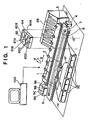
- Fig. 1 is an external appearance perspective view showing the structure of a printer having a printhead which performs printing in accordance with an ink-jet method, as a typical embodiment of the present invention;
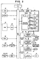
- Fig. 2 is a block diagram showing the schematic construction of a controller of the printer in Fig. 1;
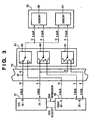
- Fig. 3 is a block diagram showing data access and
data transfer between a
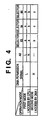
RAM 25, and aCPU 21 and aDMAC 80; - Fig. 4 is a table showing the operations of
selectors 83 to 85; - Figs. 5A, 5B, 5C, 5D and 5E are timing charts showing a time sequence of bus width changing;
- Fig. 6 is a block diagram showing data access and
data transfer between a
RAM 25, and aCPU 21 and aDMAC 80, according to another embodiment; - Fig. 7 is a table showing the operations of
selectors 83 to 85, according to the other embodiment; - Figs. 8A, 8B, 8C, 8D and 8E are timing charts showing a time sequence of bus width changing according to the other embodiment; and
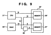
- Fig. 9 is a block diagram showing data access and data transfer between a RAM 25', and a CPU 21' and a DMAC 80' according to a modification of the embodiments shown in Fig. 3.
-
- Preferred embodiments of the present invention will now be described in detail in accordance with the accompanying drawings.
- Fig. 1 is an external appearance perspective view showing a printer having a printhead which performs printing in accordance with an ink-jet method, as a typical embodiment of the present invention.
- In Fig. 1, reference numeral 1 denotes a print paper (or a print medium such as a plastic sheet); 2 and 3, conveyance rollers provided on and under a print area of the print paper 1, for conveying the print paper 1 in the arrow A direction; 4, a sheet feed motor which drives the
conveyance rollers 2 and 3; 5, a guide shaft provided between theconveyance roller 2 and 3 and parallel to the rotational axes of theconveyance rollers 2 and 3; 6, a carriage which scans (in the arrow B direction) along the guide shaft 5; 7, a carriage motor which scan-moves thecarriage 6; and 8, a belt which transmits the driving force of thecarriage motor 7 to thecarriage 6. - The
carriage 6 holds fourprintheads 9A to 9D (hereinafter referred to as "printhead 9" generally indicating these four printheads) which respectively perform printing by discharging ink droplets in accordance with an ink-jet method. The printhead 9 is a color printhead for color image printing and comprises four printheads, 9A (Y head), 9B (M head), 9C (C head) and 9D (K head), respectively corresponding to Y (yellow) color ink, M (magenta) color ink, C (cyan) color ink and K (black) color ink, arrayed along the scanning direction of thecarriage 6. Theprintheads 9A to 9D respectively have a plurality of (e.g., 64 or 128) ink discharge orifices arrayed in a direction diagonal to the scanning direction of thecarriage 6, on their front surfaces opposite to the print surface of the print paper 1. Note that theseprintheads 9A to 9D respectively have the same logic circuit construction. - An
operation panel 64 is attached to an outer case (not shown) of the printer. Theoperation panel 64 has operation keys such as an online/off-line key 60A, aline feed key 60B, a printmode switch key 60C and areset key 60D, LED lamps such as analarm lamp 61A and apower source lamp 61B, and anLCD 65 which displays various messages. - Note that
numeral 92 denotes an ink tank containing ink for printing a desired image on the print paper 1. Theink tank 92 has four compartments respectively containing yellow (Y) ink, magenta (M) ink, cyan (C) ink and black (K) ink, corresponding to theprint heads 9A to 9D. - A controller including a CPU, ROM, RAM and the like of the printer receives an instruction signal or data signal (print information) from a host computer (hereinafter simply referred to as "host") 100, and drives the various motors and the like, and applies driving power (heating power) and energize electrothermal transducers (heaters) included in the
printheads 9A to 9D, based on the received signal. The above operation will be described in more detail below. - Fig. 2 is a block diagram showing the schematic construction of the controller of the printer in Fig. 1.
- A
CPU 21, in the form of microprocessor, is connected to thehost 100 via aninterface unit 22. TheCPU 21 accesses aROM 24 in which control programs are stored, an EEPROM 23 in which updatable control programs, processing programs, various constant data and the like are stored, and aRAM 25 in which an instruction signal (command) and a print information signal received from thehost 100 via theinterface unit 22 are stored, and controls printing operation based on the information stored in these memories. - Note that the processing executed by the above processing programs include: processing to transfer raster-format print data, received via the
interface unit 22, to a work buffer of theRAM 25; processing to convert the arrangement of the print data stored in the work buffer in consideration of the array direction of printing elements of the printhead 9 (R-C (Raster-Column) conversion); decompression processing when compressed print information is received; processing to transfer print data bitmapped in the work area of theRAM 25 to aprinthead controller 29; processing to count the number of print data (number of bits or bytes) to cause ink discharge among print data so as to estimate an ink consumption amount; processing, in case of multipath print control, to generate mask data corresponding to respective paths in theRAM 25 and transfer the mask data to the printhead 9; and processing to convert the resolution of low-resolution print data (e.g., 300 dpi), received from thehost 100 and bitmapped in the work area of theRAM 25, into a higher resolution (e.g., 300 dpi → 600 dpi) and smoothing processing to remove jaggies. - The
CPU 21 moves thecarriage 6 by driving thecarriage motor 7 via anoutput port 26 and acarriage motor controller 42, and operates the conveyance mechanism such as theconveyance rollers 2 and 3 by driving the sheet feed motor 4 via theoutput port 26 and a sheet-feed motor controller 44. Further, theCPU 21 drives theprintheads 9A to 9D via theprinthead controller 29, based on print information stored in theRAM 25, so as to print a desired image on the print paper 1. - Further, a
power circuit 28 outputs a logic driving current voltage Vcc (e.g., 5 V) to drive theCPU 21, motor driving voltage Vm (e.g., 30 V) for the various motors, a heat voltage Vh (e.g., 25 V) to drive the printhead 9, and a backup voltage VDDH for protecting the printhead 9. The heat voltage Vh is applied to the printhead 9, and the backup voltage VDDH, to theprinthead controller 29 and the printhead 9. - Further, an instruction inputted from the
operation keys 60A to 60D is transferred to theCPU 21 via aninput port 32, and when the instruction from theCPU 21 is transferred via anoutput port 36 to abuzzer generation controller 62, abuzzer 63 sounds an alarm, or when the instruction from theCPU 21 is transferred to adisplay controller 66, theLCD 65 displays a message. - Note that in Fig. 2,
numeral 70 denotes a CPU bus interconnecting the above-described various components; 80, a DMA controller (DMAC) which performs high-speed data processing controls such as clearing the memory contents, logical inversion of the memory contents and the like; and 81, a memory controller (MC) which performs access control with respect to theRAM 25 in accordance with an instruction from theCPU 21 or theDMAC 80. TheCPU bus 70 has a 16-bit physical transfer bus width, and its data transfer width is 8 bits or 16 bits in accordance with the control of theCPU 21 and theDMAC 80. - In this embodiment, the DMAC 80 performs DMA transfer when:
- (1) raster-format print data, received from the
host 100 via theinterface unit 22, is transferred to the work buffer of theRAM 25; - (2) the
RAM 25 is accessed for R-C conversion; - (3) compressed print information stored in the work
buffer of the
RAM 25 is read and decompressed; - (4) print data bitmapped in the work area of the
RAM 25 is transferred to theprinthead controller 29; - (5) print data bitmapped in the work area of the
RAM 25 is accessed to count the number of print data (number of bits or bytes) to cause ink discharge so as to estimate an ink use amount; - (6) mask data for multipath print control is transferred
from the
RAM 25 to the printhead 9; - (7) low-resolution print data bitmapped in the work area
of the
RAM 25 is accessed and resolution conversion and/or smoothing is performed; and - (8) others.
-
- Fig. 3 is a block diagram showing data access and data transfer between the
RAM 25, and theCPU 21 and theDMAC 80. - In this embodiment, the bus width when accessed by the CPU is 8 bits (N = 8), while the bus width when accessed by the
DMAC 80 is 16 bits (M = 2). - In Fig. 3,
numerals 83 to 85 denote selectors constituting the memory controller (MC) 81. Theselectors 83 to 85 respectively comprise a logic circuit used for selecting an address bus or a data bus of theRAM 25 in accordance with two first and second modes (to be described later).Numerals RAM 25 as a work area for theCPU 21 or a storage area for storing print data and the like. - Further, in Fig. 3, "Abus" denotes the address bus; "Dbus", the data bus; and "A0", the least significant bit (LSB) of the Abus. When the
RAM 25 is accessed by the CPU, thememory 86 or the 87 is selected, in accordance with the level of the bit A0. - The
CPU 21 and theDMAC 80 are connected with each other via a path other than theCPU bus 70. TheDMAC 80 issues a DMA request signal to theCPU 21, and in response to the DMA request signal, theCPU 21 returns a DMA permission signal to theDMAC 80. - Further, as shown in Fig. 3, address designation from the
CPU 21 and theDMAC 80 via the address bus (Abus) to thememories CPU 21 and thememories DMAC 80 and thememories - Fig. 4 is a table showing the operations of the
selectors 83 to 85. - First, in the first mode (normal mode) in which the
CPU 21 performs accessing operation to perform various controls of the printer, the signal level of the DMA permission signal is "L". As shown in Fig. 4, in case of A0 = "L", theselector 83 selects a terminal a, theselector 84 selects a terminal a, and theselector 85 selects a terminal a, thus thememory 86 becomes accessible. In case of A0 = "H", theselector 83 selects the terminal a, theselector 84 selects a terminal b, and theselector 85 selects a terminal b, thus thememory 87 becomes accessible. - On the other hand, when high-speed processing such as clearing of an image area of the memory by the
DMAC 80 by DMA processing is required, theDMAC 80 issues the DMA request signal to theCPU 21, requiring theCPU 21 to release theCPU bus 70 so as to use thememory CPU 21 turns the signal level of the DMA permission signal to "H" to inform that theCPU bus 70 has been released at a convenient stop of execution of instruction. - The
DMAC 80 finds that the signal level of the DMA permission signal turns to "H", and as shown in Fig. 4, theselector 83 selects a terminal b, theselector 84 selects a terminal c, and theselector 85 selects a terminal c, thus thememories - When the DMA access processing by the
DMAC 80 has been completed, theDMAC 80 resets the DMA request signal and releases an exclusive access right for theCPU bus 70. In response to this release, theCPU 21 turns the signal level of the DMA permission signal to "L" to obtain the exclusive access right for theCPU bus 70. Then, the first mode is restored. - The above operations are shown in the time sequence of Figs. 5A-5E. In Figs. 5A-5E, the exclusive access right for the
CPU bus 70 is delivered between theCPU 21 and theDMAC 80 in accordance with the signal level of the DMA permission signal transmitted between theCPU 21 and theDMAC 80, and the data bus width in memory access is dynamically changed. - Note that Fig. 5A shows a time variation of CPU access; Fig. 5B: a time variation of DMA access; Fig. 5C: a time variation of a DMA request signal; Fig. 5D: a time variation of a DMA permission signal; and Fig. 5E: a time variation of a CPU bus width.
- According to the above-described embodiment, the data bus width can be changed corresponding to memory access from the
CPU 21 or memory access from theDMAC 80, in accordance with the signal level of the DMA permission signal transmitted between theCPU 21 ad theDMAC 80. - In the above embodiment, the
CPU 21 or theDMAC 80 is operable at arbitrary timing by the time sharing operations of theCPU 21 and theDMAC 80, i.e., delivering the exclusive access right between theCPU 21 and theDMAC 80. - Next, a construction where the
CPU 21 and theDMAC 80 are concurrently operable as long as access conflict does not occur will be described. - Fig. 6 is a block diagram showing data access and data transfer between the
RAM 25, and theCPU 21 and theDMAC 80. In Fig. 6, the elements corresponding to those described in the previous embodiment have the same reference numerals and names, and the explanation of those elements will be omitted. - In the construction shown in Fig. 6, the
CPU 21 usually accesses its internal memory (not shown) but does not access thememories DMAC 80 can usually perform high-speed data processing with the 16-bit width by DMA control. That is, as shown in Fig. 7, the normal operation mode is the second mode (access by DMA), and the signal level of a Wait signal outputted from theDMAC 80 to theCPU 21 is "H". In this mode, theselector 83 selects the terminal b, theselector 84 selects the terminal c, and theselector 85 selects the terminal c. Accordingly, theDMAC 80 usually holds the exclusive access right for theCPU bus 70, and theCPU 21 and theDMAC 80 are concurrently operable unless theCPU 21 accesses thememories - In the above environment, if the
CPU 21 needs to access thememories 86 and 87 (i.e., the operation mode is changed to the first mode (access by CPU)), theCPU 21 issues an CPU access request signal. - On the other hand, in response to the CPU access request signal, the
DMAC 80 turns the signal level of the Wait signal to "L" so as to temporarily stop access by theCPU 21 to thememories memories selectors 83 to 85, and delivers the exclusive access right to theCPU 21. At a point where thememories CPU 21, theDMAC 80 turns the signal level of the Wait signal to "H". - Thereafter, the
CPU 21 finds that the signal level of the Wait signal is "H", and accesses thememories - The above operations are shown in the time sequence of Figs. 8A-8E. Figs. 8A-8E show a time sequence of memory access control in a case where the CPU accesses the
memories CPU bus 70 is delivered between theCPU 21 and theDMAC 80 in accordance with the signal level of the Wait signal transmitted between theCPU 21 and theDMAC 80, and the data bus width in memory access is dynamically changed. - Note that Fig. 8A shows a time variation of CPU access; Fig. 8B: a time variation of DMA access; Fig. 8C: a time variation of a CPU access request signal; Fig. 8D: a time variation of a Wait signal; and Fig. 8E: a time variation of a CPU bus width.
- According to this embodiment, in the construction where the DMAC usually holds the exclusive access right for the CPU bus, the access path to the memories is dynamically changed each time the CPU needs to access the memories, thereby the CPU can access the memories.
- Further, in the above two embodiments, the physical bus width of the CPU bus is 16 bits, and 8-bit data transfer and 16-bit data transfer are performed. However, this does not pose any limitation on the present invention. It may be arranged such that the CPU bus employs a bus width of 32-bit or 64-bit, for example, and 8-bit, 16-bit, 32-bit and 64-bit data transfer are performed.
- Furthermore, in the two embodiments, the ratio of data transfer width (16 bits) by the DMAC to that by the CPU (8 bits) holds an integer (in these cases, the ratio is equal to "2"). However, this does not pose any limitation on the present invention.
- For example, the ratio may be "1.5". As shown in Fig. 9, under condition that a 24-bit width CPU bus is employed, it may be arranged that a CPU accesses a memory with a 16-bit data width, while a DMAC accesses the memory with a 24-bit data width.
- Since the construction shown in Fig. 9 is quite similar to that shown in Fig. 3, the corresponding elements in Fig. 9 have the same numerals plus apostrophe ('). In Fig. 9, a numeral 88 denotes a bus width conversion circuit for converting 16-bit width data into 8-bit width data, and/or converting 8-bit width data into 16-bit width data. In this case, effective data is only lower 8 bits, higher 8 bits or any consecutive 8 bits out of the 16-bit width data.
- In the arrangement of Fig. 9, a CPU 21' has a 16-bit access width, while a DMAC 81' has a 24-bit access width. A memory 86' can input/output data with a 16-bit width, while a memory 87' can input/output data with an 8-bit width.
- Out of the 24-bit width in the DMAC 80', a 16-bit width is used for accessing a memory 86', while a remaining 8-bit width is used for accessing a memory 87'. On the other hand, the CPU 21' accesses both memories 86' and 87' with a 16-bit width. However, when the memory 87' is accessed by the CPU 21', this access is performed via the bus
width conversion circuit 88. More specifically, when the CPU 21' accesses the memory 87', the actual access width is converted to an 8-bit width from a 16-bit width by the buswidth conversion circuit 88. - Furthermore, it may be arranged that, without using the bus
width conversion circuit 88 in Fig. 9, the DMAC 80' accesses the memories 86' and 87', while the CPU 21' merely accesses the memory 86'. - It goes with saying that the ratio may be another value such as 1.333 (CPU access width: 24-bit; and DMAC access width: 32-bit).
- The embodiment described above has exemplified a printer, which comprises means (e.g., an electrothermal transducer, laser beam generator, and the like) for generating heat energy as energy utilized upon execution of ink discharge, and causes a change in state of an ink by the heat energy, among the ink-jet printers. According to this ink-jet printer and printing method, a high-density, high-precision printing operation can be attained.
- As the typical arrangement and principle of the ink-jet printing system, one practiced by use of the basic principle disclosed in, for example, U.S. Patent Nos. 4,723,129 and 4,740,796 is preferable. The above system is applicable to either one of the so-called on-demand type or a continuous type. Particularly, in the case of the on-demand type, the system is effective because, by applying at least one driving signal, which corresponds to printing information and gives a rapid temperature rise exceeding film boiling, to each of electrothermal transducers arranged in correspondence with a sheet or liquid channels holding a liquid (ink), heat energy is generated by the electrothermal transducer to effect film boiling on the heat acting surface of the printhead, and consequently, a bubble can be formed in the liquid (ink) in one-to-one correspondence with the driving signal. By discharging the liquid (ink) through a discharge opening by growth and shrinkage of the bubble, at least one droplet is formed. If the driving signal is applied as a pulse signal, the growth and shrinkage of the bubble can be attained instantly and adequately to achieve discharge of the liquid (ink) with the particularly high response characteristics.
- As the pulse driving signal, signals disclosed in U.S. Patent Nos. 4,463,359 and 4,345,262 are suitable. Note that further excellent printing can be performed by using the conditions described in U.S. Patent No. 4,313,124 of the invention which relates to the temperature rise rate of the heat acting surface.
- As an arrangement of the printhead, in addition to the arrangement as a combination of discharge nozzles, liquid channels, and electrothermal transducers (linear liquid channels or right angle liquid channels) as disclosed in the above specifications, the arrangement using U.S. Patent Nos. 4,558,333 and 4,459,600, which disclose the arrangement having a heat acting portion arranged in a flexed region is also included in the present invention. In addition, the present invention can be effectively applied to an arrangement based on Japanese Patent Laid-Open No. 59-123670 which discloses the arrangement using a slot common to a plurality of electrothermal transducers as a discharge portion of the electrothermal transducers, or Japanese Patent Laid-Open No. 59-138461 which discloses the arrangement having an opening for absorbing a pressure wave of heat energy in correspondence with a discharge portion.
- Furthermore, as a full line type printhead having a length corresponding to the width of a maximum printing medium which can be printed by the printer, either the arrangement which satisfies the full-line length by combining a plurality of printheads as disclosed in the above specification or the arrangement as a single printhead obtained by forming printheads integrally can be used.
- In addition, an exchangeable chip type printhead which can be electrically connected to the apparatus main unit and can receive an ink from the apparatus main unit upon being mounted on the apparatus main unit or a cartridge type printhead in which an ink tank is integrally arranged on the printhead itself can be applicable to the present invention.
- It is preferable to add recovery means for the printhead, preliminary auxiliary means, and the like provided as an arrangement of the printer of the present invention since the printing operation can be further stabilized. Examples of such means include, for the printhead, capping means, cleaning means, pressurization or suction means, and preliminary heating means using electrothermal transducers, another heating element, or a combination thereof. It is also effective for stable printing to provide a preliminary discharge mode which performs discharge independently of printing.
- Furthermore, in order to enhance tonality representation, it may be arranged that a plurality of printhead respectively use inks (thick color ink and thin color ink), each exhibiting the same color but different density.
- Moreover, in each of the above-mentioned embodiments of the present invention, it is assumed that the ink is a liquid. Alternatively, the present invention may employ an ink which is solid at room temperature or less and softens or liquefies at room temperature, or an ink which liquefies upon application of a use printing signal, since it is a general practice to perform temperature control of the ink itself within a range from 30°C to 70°C in the ink-jet system, so that the ink viscosity can fall within a stable discharge range.
- Furthermore, in order to improve ink-fixing, it may be arranged that a printer uses an additional printhead for discharging processed liquid to be added to ink on a printing medium prior to/after ink discharge.
- In addition, in order to prevent a temperature rise caused by heat energy by positively utilizing it as energy for causing a change in state of the ink from a solid state to a liquid state, or to prevent evaporation of the ink, an ink which is solid in a non-use state and liquefies upon heating may be used. In any case, an ink which liquefies upon application of heat energy according to a printing signal and is discharged in a liquid state, an ink which begins to solidify when it reaches a printing medium, or the like, is applicable to the present invention. In this case, an ink may be situated opposite electrothermal transducers while being held in a liquid or solid state in recess portions of a porous sheet or through holes, as described in Japanese Patent Laid-Open No. 54-56847 or 60-71260. In the present invention, the above-mentioned film boiling system is most effective for the above-mentioned inks.
- In addition, the ink-jet printer of the present invention may be used in the form of a copying machine combined with a reader, and the like, or a facsimile apparatus having a transmission/reception function in addition to an image output terminal of an information processing equipment such as a computer.
- The present invention can be applied to a system constituted by a plurality of devices (e.g., a host computer, an interface unit, a reader and a printer), or to an apparatus comprising a single device (e.g., a copying machine or a facsimile apparatus). Furthermore, it goes without saying that the invention is applicable to a case where the object of the invention is attained by supplying a program to a system or apparatus.
- As many apparently widely different embodiments of the present invention can be made without departing from the scope thereof, it is to be understood that the invention is not limited to the specific embodiments thereof except as defined in the appended claims.
Claims (26)
- A data processing method for accessing a memory (86, 77) by a CPU (21) and a DMA controller (80) via a bus (70) with an N-bit physical bus width, comprising:wherein N, N1 and N2 are respectively positive integers, N is equal to or greater than N2, characterized in that N2 is greater than N1.a first access step of executing a first mode in which said CPU accesses said memory with an N1-bit width;a second access step of executing a second mode in which said DMA controller DMA-accesses said memory with an N2-bit width; anda switching step of switching between execution of said first mode and that of said second mode, such that a selected one of said CPU and said DMA controller has an exclusive access right for said bus for executing memory access,
- The method according to claim 1, further comprising:a request step of issuing a signal to said DMA controller or said CPU, requiring said DMA controller or CPU to obtain the exclusive access right for said bus, each time said CPU or said DMA controller needs to access said memory; anda delivery step of delivering the exclusive access right for said bus from said DMA controller or said CPU, which has the exclusive access right for said bus, to said DMA controller or said CPU, which has required the exclusive access right for said bus, in accordance with the request.
- The method according to claim 2, wherein the exclusive access right for said bus usually belongs to said CPU, and said DMA controller obtains the exclusive access right for said bus each time said DMA controller needs to access to said memory.
- The method according to claim 2, wherein the exclusive access right for said bus usually belongs to said DMA controller, and said CPU obtains the exclusive access right for said bus each time said CPU needs to access to said memory.
- A data processing apparatus for accessing a memory (86,77) by a CPU (21) and a DMA controller (80) via a bus (70) with an N-bit physical bus width, comprising:wherein N, N1 and N2 are respectively positive integers, N is equal to or greater than N2, characterized in that N2 is greater than N1.first access means for executing a first mode in which said CPU accesses said memory with an N1-bit width;second access means for executing a second mode in which said DMA controller accesses said memory with an N2-bit width; andswitching means for switching between execution of said first mode and that of said second mode, such that a selected one of said CPU and said DMA controller has an exclusive access right for said bus for executing memory access,
- Apparatus as claimed in claim 5 wherein the apparatus is a printer which accesses the memory by using the CPU and the DMA controller, the printer further comprising:input means (20) for inputting print data from an external device (100);said switching means being operable to switch the exclusive access right for said bus, depending on whether executing the first mode in which said CPU accesses said memory via said bus with an N1-bit width to handle said print data, or executing the second mode in which the DMA controller accesses said memory via said bus with an N2-bit width to handle said print data; and further comprisingprinting means (6) for performing printing on a print medium (1), based on said print data.
- The printer according to claim 6, further comprising memory-access control means (81) provided between said CPU bus and said memory, for selecting an access path from said CPU to said memory or an access path from said DMA controller to said memory.
- The printer according to claim 7, wherein said CPU usually holds the exclusive access right for said CPU bus.
- The printer according to claim 8, further comprising:a first request issuance means for issuing a signal from said DMA controller to said CPU, requiring said CPU to deliver the exclusive access right for said CPU bus to said DMA controller, when said DMA controller needs to access said memory; anda first response means for issuing a permission signal to deliver the exclusive access right for said CPU bus from said CPU to said DMA controller, in response to the signal issued by said first request issuance means.
- The printer according to claim 9, further comprising:release means for resetting the signal issued by said first request issuance means and releasing the exclusive access right for said CPU bus, after said DMA controller has completed access to said memory; andre-acquisition means for re-acquiring the exclusive access right for said CPU bus for said CPU, in accordance with the reset of the signal by said release means.
- The printer according to claim 7, wherein said DMA controller usually holds the exclusive access right for said CPU bus.
- The printer according to claim 11, wherein said CPU has an internal memory.
- The printer according to claim 12, further comprising:a second request issuance means for issuing a signal from said CPU to said DMA controller, requiring said DMA to deliver the exclusive access right for said CPU bus to said CPU, when said CPU needs to access said memory; anda second response means for issuing a permission signal to deliver the exclusive access right for said CPU bus from said DMA controller to said CPU, in response to the signal issued by said second request issuance means.
- The printer according to claim 6, wherein said printing means has a printhead which performs printing.
- The printer according to claim 14, wherein said printhead is an ink-jet printhead which performs printing by discharging ink.
- The printer according to claim 15, wherein said printhead discharges the ink by utilizing thermal energy, and has a thermal energy generator for generating the thermal energy supplied to the ink.
- The printer according to claim 14, wherein said printhead is a color printhead for performing color printing.
- The printer according to claim 17, wherein said printhead includes;a first printhead unit for discharging yellow ink;a second printhead unit for discharging magenta ink;a third printhead unit for discharging cyan ink; anda fourth printhead unit for discharging black ink.
- The printer according to claim 17, wherein said printhead includes;a fifth printhead unit for discharging thin color ink; anda sixth printhead unit for discharging thick color ink, whose color is the same as that of the thin color ink.
- The printer according to claim 17, wherein said printhead includes:a seventh printhead unit for discharging ink; andan eighth printhead unit for discharging processed liquid.
- The printer according to claim 14, wherein memory access in said second mode is applied to data transfer from said memory to said printhead.
- The printer according to claim 14, wherein memory access in said second mode is applied to data transfer of print data inputted by said input means from said external device to said memory.
- The printer according to claim 14, wherein memory access in said second mode is applied to conversion of arrangement of print data in consideration of an array direction of printing elements of said printhead.
- The printer according to claim 14, wherein memory access in said second mode is applied to execution of resolution conversion and smoothing on print data inputted by said input means.
- The printer according to claim 14, wherein memory access in said second mode is applied to execution of decompression on compressed print data inputted by said input means.
- A program comprising processor implementable instructions for programming a processor to control an apparatus to carry out all the steps of a method as claimed in any one of claims 1 to 4.
Applications Claiming Priority (3)
| Application Number | Priority Date | Filing Date | Title |
|---|---|---|---|
| JP8292549A JPH10133998A (en) | 1996-11-05 | 1996-11-05 | Data processing method and recorder using the method |
| JP292549/96 | 1996-11-05 | ||
| JP29254996 | 1996-11-05 |
Publications (3)
| Publication Number | Publication Date |
|---|---|
| EP0840236A2 EP0840236A2 (en) | 1998-05-06 |
| EP0840236A3 EP0840236A3 (en) | 1998-11-04 |
| EP0840236B1 true EP0840236B1 (en) | 2003-07-23 |
Family
ID=17783214
Family Applications (1)
| Application Number | Title | Priority Date | Filing Date |
|---|---|---|---|
| EP97308726A Expired - Lifetime EP0840236B1 (en) | 1996-11-05 | 1997-10-31 | Direct memory access method and printer using such an access method |
Country Status (4)
| Country | Link |
|---|---|
| US (1) | US6144460A (en) |
| EP (1) | EP0840236B1 (en) |
| JP (1) | JPH10133998A (en) |
| DE (1) | DE69723646T2 (en) |
Families Citing this family (8)
| Publication number | Priority date | Publication date | Assignee | Title |
|---|---|---|---|---|
| JP2000022910A (en) * | 1998-06-26 | 2000-01-21 | Canon Inc | Facsimile machine and record controlling method |
| CN1157651C (en) * | 2000-01-12 | 2004-07-14 | 精工爱普生株式会社 | Data output control device and personal digital assistant |
| DE60123342T2 (en) * | 2000-01-12 | 2007-04-12 | Seiko Epson Corp. | PERSONAL DIGITAL TERMINAL AND OUTPUT CONTROL SYSTEM |
| AU2552101A (en) * | 2000-01-12 | 2001-07-24 | Seiko Epson Corporation | Data output control device and personal digital terminal |
| JP4054598B2 (en) | 2002-04-25 | 2008-02-27 | キヤノン株式会社 | Memory control circuit, DMA request block, and memory access system |
| KR100450680B1 (en) * | 2002-07-29 | 2004-10-01 | 삼성전자주식회사 | Memory controller for increasing bus bandwidth, data transmitting method and computer system having the same |
| JP2004358799A (en) * | 2003-06-04 | 2004-12-24 | Canon Inc | Carriage driving control method |
| KR100551480B1 (en) * | 2004-10-25 | 2006-02-13 | 삼성전자주식회사 | Memory device configured between processor and non-volatile memory, data transmitting and receiving method among memory device, processor and non-volatile memory |
Family Cites Families (30)
| Publication number | Priority date | Publication date | Assignee | Title |
|---|---|---|---|---|
| US4122520A (en) * | 1977-05-23 | 1978-10-24 | General Electric Company | Microcomputer controller and direct memory access apparatus therefor |
| CA1127227A (en) * | 1977-10-03 | 1982-07-06 | Ichiro Endo | Liquid jet recording process and apparatus therefor |
| US4330787A (en) * | 1978-10-31 | 1982-05-18 | Canon Kabushiki Kaisha | Liquid jet recording device |
| US4345262A (en) * | 1979-02-19 | 1982-08-17 | Canon Kabushiki Kaisha | Ink jet recording method |
| US4463359A (en) * | 1979-04-02 | 1984-07-31 | Canon Kabushiki Kaisha | Droplet generating method and apparatus thereof |
| US4313124A (en) * | 1979-05-18 | 1982-01-26 | Canon Kabushiki Kaisha | Liquid jet recording process and liquid jet recording head |
| JPS5779551A (en) * | 1980-11-06 | 1982-05-18 | Nec Corp | Information transfer device |
| DE3104941A1 (en) * | 1981-02-11 | 1982-08-26 | Siemens AG, 1000 Berlin und 8000 München | MICROCALCULATOR SYSTEM FOR RAPIDLY DETECTING LABEL BLOCKS |
| US4558333A (en) * | 1981-07-09 | 1985-12-10 | Canon Kabushiki Kaisha | Liquid jet recording head |
| JPS59123670A (en) * | 1982-12-28 | 1984-07-17 | Canon Inc | Ink jet head |
| JPS59138461A (en) * | 1983-01-28 | 1984-08-08 | Canon Inc | Liquid jet recording apparatus |
| JPS6071260A (en) * | 1983-09-28 | 1985-04-23 | Erumu:Kk | Recorder |
| JPH01258163A (en) * | 1988-04-08 | 1989-10-16 | Fujitsu Ltd | Direct memory access controller |
| JPH01277928A (en) * | 1988-04-30 | 1989-11-08 | Oki Electric Ind Co Ltd | Printer |
| US4965748A (en) * | 1989-07-12 | 1990-10-23 | Ricoh Company, Ltd. | Laser printer controller flexible frame buffer architecture which allows offsetting different input/output data widths |
| US4977519A (en) * | 1989-07-12 | 1990-12-11 | Ricoh Company, Ltd. | Laser printer controller flexible frame buffer architecture which allows software to change X and Y dimensions of the buffer |
| JP2504206B2 (en) * | 1989-07-27 | 1996-06-05 | 三菱電機株式会社 | Bus controller |
| EP0427407A3 (en) * | 1989-11-03 | 1993-03-10 | Compaq Computer Corporation | Parallel port with direct memory access capabilities |
| US5119480A (en) * | 1989-11-13 | 1992-06-02 | International Business Machines Corporation | Bus master interface circuit with transparent preemption of a data transfer operation |
| US5072365A (en) * | 1989-12-27 | 1991-12-10 | Motorola, Inc. | Direct memory access controller using prioritized interrupts for varying bus mastership |
| US5333294A (en) * | 1990-10-09 | 1994-07-26 | Compaq Computer Corporation | Configurable data width direct memory access device with a read address counter and a write address counter which increments the addresses based on the desired data transfer width |
| JPH04363745A (en) * | 1991-05-17 | 1992-12-16 | Toshiba Corp | Dma controller |
| DE69224887T2 (en) * | 1991-07-08 | 1998-07-23 | Seiko Epson Corp | SINGLE-CHIP SIDE PRINTER CONTROL CIRCUIT |
| US5630163A (en) * | 1991-08-09 | 1997-05-13 | Vadem Corporation | Computer having a single bus supporting multiple bus architectures operating with different bus parameters |
| AU2142492A (en) * | 1991-12-09 | 1993-07-19 | Tandy Corporation | Direct memory access interface for buses of different width |
| US5579453A (en) * | 1994-12-16 | 1996-11-26 | Xerox Corporation | Smart direct memory access controller |
| US5953132A (en) * | 1995-07-18 | 1999-09-14 | Canon Kabushiki Kaisha | Image communication apparatus with enhanced utilization of CPU |
| JP3116989B2 (en) * | 1995-10-16 | 2000-12-11 | セイコーエプソン株式会社 | Decompression device for compressed binary image data |
| US5689659A (en) * | 1995-10-30 | 1997-11-18 | Motorola, Inc. | Method and apparatus for bursting operand transfers during dynamic bus sizing |
| US5793397A (en) * | 1995-11-03 | 1998-08-11 | Accent Color Sciences, Inc. | Printer assembly |
-
1996
- 1996-11-05 JP JP8292549A patent/JPH10133998A/en active Pending
-
1997
- 1997-10-30 US US08/961,244 patent/US6144460A/en not_active Expired - Lifetime
- 1997-10-31 DE DE69723646T patent/DE69723646T2/en not_active Expired - Lifetime
- 1997-10-31 EP EP97308726A patent/EP0840236B1/en not_active Expired - Lifetime
Also Published As
| Publication number | Publication date |
|---|---|
| US6144460A (en) | 2000-11-07 |
| DE69723646D1 (en) | 2003-08-28 |
| DE69723646T2 (en) | 2004-06-03 |
| JPH10133998A (en) | 1998-05-22 |
| EP0840236A2 (en) | 1998-05-06 |
| EP0840236A3 (en) | 1998-11-04 |
Similar Documents
| Publication | Publication Date | Title |
|---|---|---|
| US6371588B1 (en) | Printhead and printing apparatus using printhead | |
| EP0678386B1 (en) | Printing head, and printer and printing method using the printing head | |
| US20020051024A1 (en) | Printing apparatus and power consumption reduction method of printing apparatus | |
| EP0840236B1 (en) | Direct memory access method and printer using such an access method | |
| US20020186273A1 (en) | Image printing apparatus, control method therefor, storage medium and program | |
| US20010022597A1 (en) | Printing apparatus and method of controlling power supply thereof | |
| US7315393B2 (en) | Printing system, printer driver, and printing method | |
| US5963713A (en) | Printer using direct memory access and refreshing | |
| EP0780789B1 (en) | Apparatus and method for printing | |
| JP3323762B2 (en) | Recording device | |
| US6782481B2 (en) | Method and apparatus for supplying battery power to a timer circuit within a printer while the printer is powered off | |
| EP0856985B1 (en) | Printing apparatus and printing control method | |
| JP3962591B2 (en) | Ink jet printer and control method of ink jet printer | |
| JP3517570B2 (en) | Recording apparatus and recording control method | |
| JPH09169112A (en) | Recording apparatus | |
| EP1116587A1 (en) | Printing apparatus and printing method | |
| US5956472A (en) | Data processing method and data processing apparatus and printer using data processing apparatus | |
| US7206095B2 (en) | Printing apparatus and method | |
| US6585354B2 (en) | Image printing apparatus and method | |
| JP2001026150A (en) | Address converting circuit and recording apparatus using the same | |
| JP2002292944A (en) | Image recording apparatus and controlling method therefor | |
| JPH1110841A (en) | Recorder | |
| JP2000085127A (en) | Recording data processing method and recording device | |
| JP2001171118A (en) | Recorder | |
| JPH06166176A (en) | Ink jet recording device |
Legal Events
| Date | Code | Title | Description |
|---|---|---|---|
| PUAI | Public reference made under article 153(3) epc to a published international application that has entered the european phase |
Free format text: ORIGINAL CODE: 0009012 |
|
| AK | Designated contracting states |
Kind code of ref document: A2 Designated state(s): DE ES FR GB IT NL |
|
| AX | Request for extension of the european patent |
Free format text: AL;LT;LV;RO;SI |
|
| PUAL | Search report despatched |
Free format text: ORIGINAL CODE: 0009013 |
|
| AK | Designated contracting states |
Kind code of ref document: A3 Designated state(s): AT BE CH DE DK ES FI FR GB GR IE IT LI LU MC NL PT SE |
|
| AX | Request for extension of the european patent |
Free format text: AL;LT;LV;RO;SI |
|
| 17P | Request for examination filed |
Effective date: 19990318 |
|
| AKX | Designation fees paid |
Free format text: DE ES FR GB IT NL |
|
| 17Q | First examination report despatched |
Effective date: 20020222 |
|
| GRAH | Despatch of communication of intention to grant a patent |
Free format text: ORIGINAL CODE: EPIDOS IGRA |
|
| GRAH | Despatch of communication of intention to grant a patent |
Free format text: ORIGINAL CODE: EPIDOS IGRA |
|
| GRAA | (expected) grant |
Free format text: ORIGINAL CODE: 0009210 |
|
| AK | Designated contracting states |
Designated state(s): DE ES FR GB IT NL |
|
| PG25 | Lapsed in a contracting state [announced via postgrant information from national office to epo] |
Ref country code: NL Free format text: LAPSE BECAUSE OF FAILURE TO SUBMIT A TRANSLATION OF THE DESCRIPTION OR TO PAY THE FEE WITHIN THE PRESCRIBED TIME-LIMIT Effective date: 20030723 |
|
| REG | Reference to a national code |
Ref country code: GB Ref legal event code: FG4D |
|
| REF | Corresponds to: |
Ref document number: 69723646 Country of ref document: DE Date of ref document: 20030828 Kind code of ref document: P |
|
| PG25 | Lapsed in a contracting state [announced via postgrant information from national office to epo] |
Ref country code: ES Free format text: LAPSE BECAUSE OF FAILURE TO SUBMIT A TRANSLATION OF THE DESCRIPTION OR TO PAY THE FEE WITHIN THE PRESCRIBED TIME-LIMIT Effective date: 20031103 |
|
| NLV1 | Nl: lapsed or annulled due to failure to fulfill the requirements of art. 29p and 29m of the patents act | ||
| ET | Fr: translation filed | ||
| PLBE | No opposition filed within time limit |
Free format text: ORIGINAL CODE: 0009261 |
|
| STAA | Information on the status of an ep patent application or granted ep patent |
Free format text: STATUS: NO OPPOSITION FILED WITHIN TIME LIMIT |
|
| 26N | No opposition filed |
Effective date: 20040426 |
|
| PGFP | Annual fee paid to national office [announced via postgrant information from national office to epo] |
Ref country code: IT Payment date: 20081020 Year of fee payment: 12 |
|
| PGFP | Annual fee paid to national office [announced via postgrant information from national office to epo] |
Ref country code: FR Payment date: 20081024 Year of fee payment: 12 |
|
| REG | Reference to a national code |
Ref country code: FR Ref legal event code: ST Effective date: 20100630 |
|
| PG25 | Lapsed in a contracting state [announced via postgrant information from national office to epo] |
Ref country code: FR Free format text: LAPSE BECAUSE OF NON-PAYMENT OF DUE FEES Effective date: 20091102 |
|
| PG25 | Lapsed in a contracting state [announced via postgrant information from national office to epo] |
Ref country code: IT Free format text: LAPSE BECAUSE OF NON-PAYMENT OF DUE FEES Effective date: 20091031 |
|
| PGFP | Annual fee paid to national office [announced via postgrant information from national office to epo] |
Ref country code: DE Payment date: 20141031 Year of fee payment: 18 Ref country code: GB Payment date: 20141021 Year of fee payment: 18 |
|
| REG | Reference to a national code |
Ref country code: DE Ref legal event code: R119 Ref document number: 69723646 Country of ref document: DE |
|
| GBPC | Gb: european patent ceased through non-payment of renewal fee |
Effective date: 20151031 |
|
| PG25 | Lapsed in a contracting state [announced via postgrant information from national office to epo] |
Ref country code: GB Free format text: LAPSE BECAUSE OF NON-PAYMENT OF DUE FEES Effective date: 20151031 Ref country code: DE Free format text: LAPSE BECAUSE OF NON-PAYMENT OF DUE FEES Effective date: 20160503 |