EP0851599A1 - Inexpensive modulated backscatter reflector - Google Patents
Inexpensive modulated backscatter reflector Download PDFInfo
- Publication number
- EP0851599A1 EP0851599A1 EP97310160A EP97310160A EP0851599A1 EP 0851599 A1 EP0851599 A1 EP 0851599A1 EP 97310160 A EP97310160 A EP 97310160A EP 97310160 A EP97310160 A EP 97310160A EP 0851599 A1 EP0851599 A1 EP 0851599A1
- Authority
- EP
- European Patent Office
- Prior art keywords
- tag
- antenna
- gate
- signal
- inexpensive
- Prior art date
- Legal status (The legal status is an assumption and is not a legal conclusion. Google has not performed a legal analysis and makes no representation as to the accuracy of the status listed.)
- Granted
Links
Images


Classifications
-
- G—PHYSICS
- G01—MEASURING; TESTING
- G01S—RADIO DIRECTION-FINDING; RADIO NAVIGATION; DETERMINING DISTANCE OR VELOCITY BY USE OF RADIO WAVES; LOCATING OR PRESENCE-DETECTING BY USE OF THE REFLECTION OR RERADIATION OF RADIO WAVES; ANALOGOUS ARRANGEMENTS USING OTHER WAVES
- G01S13/00—Systems using the reflection or reradiation of radio waves, e.g. radar systems; Analogous systems using reflection or reradiation of waves whose nature or wavelength is irrelevant or unspecified
- G01S13/74—Systems using reradiation of radio waves, e.g. secondary radar systems; Analogous systems
- G01S13/75—Systems using reradiation of radio waves, e.g. secondary radar systems; Analogous systems using transponders powered from received waves, e.g. using passive transponders, or using passive reflectors
- G01S13/751—Systems using reradiation of radio waves, e.g. secondary radar systems; Analogous systems using transponders powered from received waves, e.g. using passive transponders, or using passive reflectors wherein the responder or reflector radiates a coded signal
- G01S13/758—Systems using reradiation of radio waves, e.g. secondary radar systems; Analogous systems using transponders powered from received waves, e.g. using passive transponders, or using passive reflectors wherein the responder or reflector radiates a coded signal using a signal generator powered by the interrogation signal
-
- G—PHYSICS
- G06—COMPUTING; CALCULATING OR COUNTING
- G06K—GRAPHICAL DATA READING; PRESENTATION OF DATA; RECORD CARRIERS; HANDLING RECORD CARRIERS
- G06K19/00—Record carriers for use with machines and with at least a part designed to carry digital markings
- G06K19/06—Record carriers for use with machines and with at least a part designed to carry digital markings characterised by the kind of the digital marking, e.g. shape, nature, code
- G06K19/067—Record carriers with conductive marks, printed circuits or semiconductor circuit elements, e.g. credit or identity cards also with resonating or responding marks without active components
- G06K19/07—Record carriers with conductive marks, printed circuits or semiconductor circuit elements, e.g. credit or identity cards also with resonating or responding marks without active components with integrated circuit chips
- G06K19/0723—Record carriers with conductive marks, printed circuits or semiconductor circuit elements, e.g. credit or identity cards also with resonating or responding marks without active components with integrated circuit chips the record carrier comprising an arrangement for non-contact communication, e.g. wireless communication circuits on transponder cards, non-contact smart cards or RFIDs
-
- G—PHYSICS
- G01—MEASURING; TESTING
- G01S—RADIO DIRECTION-FINDING; RADIO NAVIGATION; DETERMINING DISTANCE OR VELOCITY BY USE OF RADIO WAVES; LOCATING OR PRESENCE-DETECTING BY USE OF THE REFLECTION OR RERADIATION OF RADIO WAVES; ANALOGOUS ARRANGEMENTS USING OTHER WAVES
- G01S13/00—Systems using the reflection or reradiation of radio waves, e.g. radar systems; Analogous systems using reflection or reradiation of waves whose nature or wavelength is irrelevant or unspecified
- G01S13/74—Systems using reradiation of radio waves, e.g. secondary radar systems; Analogous systems
- G01S13/75—Systems using reradiation of radio waves, e.g. secondary radar systems; Analogous systems using transponders powered from received waves, e.g. using passive transponders, or using passive reflectors
- G01S13/751—Systems using reradiation of radio waves, e.g. secondary radar systems; Analogous systems using transponders powered from received waves, e.g. using passive transponders, or using passive reflectors wherein the responder or reflector radiates a coded signal
- G01S13/756—Systems using reradiation of radio waves, e.g. secondary radar systems; Analogous systems using transponders powered from received waves, e.g. using passive transponders, or using passive reflectors wherein the responder or reflector radiates a coded signal using a signal generator for modifying the reflectivity of the reflector
Definitions
- This invention relates to wireless communication systems and, more particularly, to a wireless communication system using modulated backscatter technology.
- RFID Radio Frequency Identification
- MMS Modulated BackScatter
- the Interrogator communicates to the Tags using modulated radio signals.
- the Tags communicate with the Interrogator by reflecting (backscattering) back to the Interrogator a Continuous Wave (CW) carrier signal originally transmitted by the Interrogator.
- CW Continuous Wave
- the Tag has an antenna which it uses to receive messages from the Interrogator and to reflect messages back to the Interrogator. After transmitting a message to the Tag, the Interrogator transmits the CW carrier signal to the Tag. The Tag uses the CW carrier signal to respond to the Interrogator message by reflecting or backscattering the CW carrier signal with the modulated subcarrier signal.
- the CW carrier signal is typically a signal in the microwave frequency range.
- the reflected or backscattered CW carrier signal is modulated by the Tag with a modulating signal that is generated at the Tag.
- the Tag antenna radar cross-section i.e., the effective reflective area of the antenna
- the Tag antenna radar cross-section i.e., the effective reflective area of the antenna
- the diode is modulated by alternately biasing ON and OFF a high-quality microwave diode attached to the antenna.
- the diode When the diode is in its conducting state, i.e., the diode is biased in the ON state, the diode acts as an RF short circuit. When in the OFF state, the diode acts as an RF open circuit.
- the impedance or reflectivity of the antenna is modulated which causes the antenna to alternately reflect and absorb the impinging CW carrier signal.
- the conducting diode Connected to the correct location on the antenna, such as a feedpoint of an antenna, the conducting diode changes a tuned antenna into a detuned antenna causing the antenna to reflect rather than absorb the impinging CW RF signal.
- a modulated backscatter RFID tag is sometimes referred to as a passive radio tag in that it reflects and modulates a continuous wave (CW) radio signal with which it is illuminated in an analogous way to a mirror which can be used for communicating by flashing the light from the sun to an observer at a distance.
- FIG. 1 illustrates a typical read-only modulated backscatter RFID system comprising an Interrogator 105 and a Tag 101.
- Tag 101 comprises a microprocessor 102, a modulator 103 and an antenna 104.
- the Reader RF Unit 108 Within the Interrogator 105, the Reader RF Unit 108 generates and transmits a CW signal by means of the Transmit Antenna 106.
- This signal illuminates the Tag Antenna 104 which reflects (or backscatters) a portion of the incident signal.
- the reflection coefficient or reflectivity of the antenna a parameter well known to those in the field of antenna design which indicates an antenna's ability to reflect energy within a certain frequency range, is modulated directly by a modulating signal.
- the reflection coefficient of the Tag Antenna 104 is switched between being a good absorber of energy to a good reflector in a time-varying pattern (modulating signal) determined by the data stored in the tag memory.
- the variable reflection coefficient of the Tag Antenna 104 modulates the backscattered RF signal.
- This backscattered signal is captured by the Interrogator Receive Antenna 107, amplified and down-converted by the Reader RF Unit 108 and the data recovered by the Demodulator 109, Digital Signal Processor (DSP 110 if present) and Microprocessor ( ⁇ P) 111.
- DSP 110 Digital Signal Processor
- ⁇ P Microprocessor
- Tag Antenna 104 modulates the reflected RF signal. This, in turn, depends upon the Tag Antenna 104 radar cross-section the impedance matching between the Tag Antenna 104, the Tag Modulator 103, and the quality of the Tag Modulator 103.
- the Tag Modulator 103 for optimum system performance, is usually a high-quality microwave semiconductor, often a switching diode. For a inexpensive Tag 101, this device alone can constitute a major part of the total Tag cost. Thus, in order to significantly reduce the cost of manufacture of the Tag, the cost of Modulator 103 must be reduced while still maintaining acceptable system sensitivity and range.
- RFID system application in which high sensitivity and long range are less important that low cost.
- One such class of application includes tracking airline luggage. Therefore, there is a need to design a relatively inexpensive Tag for such systems.
- an inexpensive Tag design used in an RFID communication system that uses MBS comprises a data storage device, a variable impedance semiconductor gate electrically connected to the data storage device for receiving the stored information and an antenna having a certain reflectivity.
- the antenna is electrically connected to the variable impedance device which modulates the reflectivity of the antenna in accordance with the received information.
- all of the parts of the Tag are incorporated into an integrated circuit which also modulates the reflectivity of the antenna.
- the present invention claims an inexpensive modulator for an RFID system for short range applications.
- An inexpensive Complementary Metal Oxide Semiconductor (CMOS) gate is used in place of the typically used high quality diode to modulate the reflectivity or impedance of an MBS antenna simplifying the Tag design and significantly reducing cost of manufacture of the Tag and overall system cost.
- CMOS Complementary Metal Oxide Semiconductor
- FIG. 2 shows a block diagram of the present invention, a simple read-only tag, for applications such as tracking airline luggage.
- Information such as encoded data stored in the Tag Shift Register 203, is used to drive a Variable Impedance device 202, a CMOS gate in this embodiment, coupled to the Tag Antenna 201.
- Other Data Storage devices such as a Read Only Memory (ROM) or similar devices can be used instead of a shift register to drive the Variable Impedance device 202.
- ROM Read Only Memory
- Variable Impedance device 202 receives the encoded data and modulates the reflectivity of Antenna 201 in accordance with the encoded data.
- the Power Module 204 in this embodiment, is either an inexpensive battery or a rectifier which draws its power from the illuminating RF.
- This invention would constitute an important element of a low cost, read-only RFID Tag for short range applications such as airline baggage tracking.
- CMOS Gate 202 for this purpose has the advantage over other modulation schemes of low cost and low power usage.
- This type of Tag is used for short range applications (less than 2 meters) due to the less efficient Variable Impedance device and, in the case in which the Tag is RF-powered, rapid fall off of RF power with distance from the Interrogator.
- the use of an inexpensive CMOS Gate 202 as a modulating element for a Modulated Backscatter RFID Tag such as the one depicted in FIG.1 will now be described.
- FIG. 3 is a block diagram of a simple test circuit which demonstrates how a simple CMOS Inverter Gate 302 can be used as a modulating element in an MBS Tag such as the one depicted in FIG. 2.
- an Inverter Gate 302 from a 74HC04 high-speed CMOS integrated circuit 301 was used, driven by a baseband signal 304, which in this case was a Square Wave Signal from a signal generator.
- the output of the Inverter Gate 302 in this instance, was connected to the feed-point of a 1/4-wave Patch Antenna 306.
- Other antennas have been tested with this circuit including bowtie, loop and 1/2-wave dipole configurations.
- a microwave Sweep Oscillator (HP 8350B) 401 operating at a 2.45 GHz CW frequency, drives a Power Amplifier (PM2104) 402 with an output of +30 dBm (1 watt).
- PM2104 Power Amplifier
- This signal is transmitted by a Planar Antenna 403 with an 8.5 dBi gain, illuminating the Circuit Under Test 412 (Tag circuit).
- the output of circuit 412 is buffered by inverter gate 410 which also drives antenna 411.
- the backscatter signal is received by a Receive Antenna 404 and amplified by a Low Noise Amplifier (LNA) 405.
- LNA Low Noise Amplifier
- the LNA output is mixed with an attenuated (-20 dB) Sample 409 of the original CW transmit signal in a Quadrature IF Mixer (QIFM) 406.
- QIFM 406 is a baseband replica of the signal which modulates the reflectivity of the antenna on the test circuit or Tag. This weak baseband signal is amplified and displayed on a Spectrum Analyzer (HP 3562A) 408.
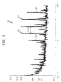
- FIG. 5 shows the Spectrum Analyzer plot 501 of one of the tests performed with the circuit of FIG. 3.
- the drive signal i.e., baseband signal 304
- the plot displays peaks 502 and 503 not only at 60 and 80 kHz but peaks 504 at 10 kHz sidebands generated by the switching rate.
- Additional tests were conducted with a Exclusive OR (XOR) gate instead of an inverter and with a different drive signal. All tests yielded similar results.
- XOR Exclusive OR
- FIG. 6 shows a battery-powered test circuit designed to measure directly the impedance change of a CMOS Inverter Gate from a 74HC04 high-speed CMOS integrated circuit 601 at the microwave frequency range of interest.
- the output of CMOS inverter 602 is connected to an RF coaxial connector (SMA).
- the Gate Input 609 is connected to a Bias Switch 603 with which to change the input bias from high to low.
- One end of Resistor 604 is connected to input 609 of gate 602 while the other end of Resistor 604 is connected to digital ground 606.
- One end of Bias Switch 603 is connected to +V volts where V is equal to a voltage level recognized as a logical HIGH by CMOS gates.
- V is typically equal to +5 volts .
- FIG. 8 is a block diagram of a simulated single-chip CMOS RFID Tag, assemble with discrete 74HC integrated circuits. It differs from a fully functional Tag 101 in that is has Manual Programming Switches 807 and an onboard battery (not shown).
- the circuit includes a 27.7 kHz Clock 801 which generates the Subcarrier 802. This frequency is divided by 16 by circuit 803 whose output toggles a D flip-flop (not shown) resulting in 870 Hz clock 804 which drives Programmable Shift Register 806.
- Reset clock circuit 805 is used to reset circuits 806 and 802 when the Tag is initially powered.
- the Programmable Shift Register 806 Output Datastream 808 and the Subcarrier 802 are applied to the two inputs of an XOR Gate 809, resulting in an output carrier whose phase alternates with each alternation of the data stream.
- This gate output signal which uses Binary Phase Shift Keyed modulation (BPSK), is buffered by a single Inverter Gate 810 which is connected to one leg of a Bowtie Antenna 812, tuned to about 2.5 GHz. The other antenna leg is connected to ground.
- BPSK Binary Phase Shift Keyed modulation
- the circuit is tested as displayed in FIG. 4, as previously described above in the test performed on the circuit in FIG. 3.
- a +30 dBm CW 2.45 GHz signal from the Transmit Antenna 403 illuminates the Bowtie Antenna 411.
- the backscattered signal, BPSK-modulated by the CMOS Gate/Antenna combination is picked up by the Receive Antenna 404 and mixed down to the subcarrier frequency. This signal, after amplification, is displayed on a Spectrum Analyzer 408.
- FIG. 9 displays the signals generated within the Simulated Tag operating at a clock frequency of 27.7 kHz using an XOR gate as a modulator as shown in FIG. 8.
- the top trace is the unmodulated Raw Clock 901. Beneath this is the Secondary Clock trace 902, which is the primary frequency divided by 16.
- the Secondary Clock 902 is used to strobe the shift register data output to the XOR modulator gate.
- the third trace, the Partial Modulation Sequence 903 is a portion of this data sequence showing two transitions.
- the final trace, the Modulated Carrier 904, is the BPSK modulated carrier output from the XOR gate. Notice the change of phase corresponding to each transition of the data. This is the signal which drives the CMOS Inverter Gate 810 of FIG. 8 whose output is the modulating element connected to the Tag Antenna 812.
- FIG. 10 is a Spectrum Analyzer display of the downconverted MBS signal. Clearly evident is the Subcarrier Frequency (27.7 kHz) 1001 and the side bands 1002 at odd intervals of 870 Hz created by modulating data stream 808 (see FIG. 8) of the Tag unit shown in FIG. 2.
Abstract
Description
Claims (10)
- A Tag for an RFID communication system using MBS
CHARACTERIZED BYa data storage device (203) containing information;a variable impedance device (202) electrically connected to the data storage device allowing the variable impedance device to receive the information; andan antenna (201) having a certain reflectivity and electrically connected to the variable impedance device such that the variable impedance device modulates the reflectivity of the antenna accordance with the received information. - The Tag of claim 1 wherein the variable impedance device is CMOS gate.
- The Tag of claim 1 wherein the data storage device is a shift register.
- The Tag of claim 2 wherein the CMOS gate circuit is an inverter gate.
- The Tag of claim 2 wherein the CMOS gate is a XOR gate.
- The Tag of claim 2 wherein the CMOS gate is an OR gate.
- The Tag of claim 2 wherein the CMOS gate is an AND gate.
- A Tag for an RFID communication system using MBS CHARACTERIZED BYan antenna (201, 306) having a certain reflectivity; andan integrated circuit electrically connected to the antenna for modulating the reflectivity of the antenna in accordance with information stored in the integrated circuit.
- The Tag of claim 8 wherein the integrated circuit comprises a data storage device (203) for storing the information and a variable impedance device (202) connected to the data storage device for modulating the reflectivity of the antenna in accordance with the stored information.
- The Tag of claim 9 wherein the data storage device and the variable impedance device CHARACTERIZED BY gates.
Applications Claiming Priority (2)
| Application Number | Priority Date | Filing Date | Title |
|---|---|---|---|
| US774499 | 1996-12-31 | ||
| US08/774,499 US6243012B1 (en) | 1996-12-31 | 1996-12-31 | Inexpensive modulated backscatter reflector |
Publications (2)
| Publication Number | Publication Date |
|---|---|
| EP0851599A1 true EP0851599A1 (en) | 1998-07-01 |
| EP0851599B1 EP0851599B1 (en) | 2003-03-26 |
Family
ID=25101440
Family Applications (1)
| Application Number | Title | Priority Date | Filing Date |
|---|---|---|---|
| EP97310160A Expired - Lifetime EP0851599B1 (en) | 1996-12-31 | 1997-12-16 | Inexpensive modulated backscatter reflector |
Country Status (6)
| Country | Link |
|---|---|
| US (1) | US6243012B1 (en) |
| EP (1) | EP0851599B1 (en) |
| JP (1) | JPH10224262A (en) |
| KR (1) | KR19980064803A (en) |
| CA (1) | CA2222320A1 (en) |
| DE (1) | DE69720170T2 (en) |
Cited By (8)
| Publication number | Priority date | Publication date | Assignee | Title |
|---|---|---|---|---|
| WO2000049564A1 (en) * | 1999-02-17 | 2000-08-24 | Microchip Technology Incorporated | Radio frequency identification (rfid) security tag for merchandise and method therefor |
| EP1055943A2 (en) * | 1999-05-24 | 2000-11-29 | Hitachi, Ltd. | A wireless tag, its manufacturing and its layout |
| EP1170695A1 (en) * | 2000-07-04 | 2002-01-09 | Texas Instruments Deutschland Gmbh | Trimming circuit for trimming of film type antennas |
| EP2330538A1 (en) | 2009-11-30 | 2011-06-08 | Nxp B.V. | Radio frequency transponder |
| WO2013170338A1 (en) * | 2012-05-14 | 2013-11-21 | Tag-Comm Inc. | Apparatus for generating dedicated data channels in backscatter rfid system using band -pass delta sygma modulator |
| WO2013170337A1 (en) * | 2012-05-14 | 2013-11-21 | Tag-Comm Inc. | Apparatus for generating dedicated data channels in backscatter rfid system using low pass delta sygma modulator |
| NO341680B1 (en) * | 2004-02-27 | 2017-12-18 | Hitoshi Kitayoshi | RF identification label device |
| US10079704B2 (en) | 2014-09-22 | 2018-09-18 | Drnc Holdings, Inc. | Transmission apparatus for a wireless device using delta-sigma modulation |
Families Citing this family (85)
| Publication number | Priority date | Publication date | Assignee | Title |
|---|---|---|---|---|
| US6118789A (en) * | 1998-02-19 | 2000-09-12 | Micron Technology, Inc. | Method of addressing messages and communications system |
| US6356535B1 (en) * | 1998-02-04 | 2002-03-12 | Micron Technology, Inc. | Communication systems and methods of communicating |
| US6061344A (en) | 1998-02-19 | 2000-05-09 | Micron Technology, Inc. | Method of addressing messages and communications system |
| USRE43382E1 (en) | 1998-02-19 | 2012-05-15 | Round Rock Research, Llc | Method of addressing messages and communications systems |
| US6072801A (en) | 1998-02-19 | 2000-06-06 | Micron Technology, Inc. | Method of addressing messages, method of establishing wireless communications, and communications system |
| US6275476B1 (en) | 1998-02-19 | 2001-08-14 | Micron Technology, Inc. | Method of addressing messages and communications system |
| US7710273B2 (en) * | 1999-09-02 | 2010-05-04 | Round Rock Research, Llc | Remote communication devices, radio frequency identification devices, wireless communication systems, wireless communication methods, radio frequency identification device communication methods, and methods of forming a remote communication device |
| US6798349B1 (en) * | 1999-10-04 | 2004-09-28 | Xerox Corporation | Passive microwave tag identification system |
| US6838989B1 (en) * | 1999-12-22 | 2005-01-04 | Intermec Ip Corp. | RFID transponder having active backscatter amplifier for re-transmitting a received signal |
| US7006014B1 (en) * | 2000-10-17 | 2006-02-28 | Henty David L | Computer system with passive wireless keyboard |
| GB0122163D0 (en) * | 2001-09-13 | 2001-10-31 | Tagtec Ltd | Wireless communication system |
| US7003167B2 (en) * | 2001-11-01 | 2006-02-21 | Hewlett-Packard Development Company, L.P. | Single-pass guaranteed-fit data compression using rate feedback |
| US6970089B2 (en) | 2002-07-03 | 2005-11-29 | Battelle Memorial Institute K1-53 | Full-spectrum passive communication system and method |
| US7088964B2 (en) * | 2002-10-02 | 2006-08-08 | University Of Florida Research Foundation, Inc. | Single chip radio with integrated antenna |
| DE10254202B4 (en) * | 2002-11-20 | 2006-05-18 | Siemens Ag | Device and method for detecting the seat occupancy in a vehicle |
| DE10254200B4 (en) * | 2002-11-20 | 2006-04-20 | Siemens Ag | Device and method for detecting the seat occupancy in a vehicle |
| DE10254197B4 (en) * | 2002-11-20 | 2006-05-04 | Siemens Ag | Device and method for detecting the seat occupancy in a vehicle |
| US7023341B2 (en) * | 2003-02-03 | 2006-04-04 | Ingrid, Inc. | RFID reader for a security network |
| US7511614B2 (en) * | 2003-02-03 | 2009-03-31 | Ingrid, Inc. | Portable telephone in a security network |
| US6888459B2 (en) * | 2003-02-03 | 2005-05-03 | Louis A. Stilp | RFID based security system |
| US20060132302A1 (en) * | 2003-02-03 | 2006-06-22 | Stilp Louis A | Power management of transponders and sensors in an RFID security network |
| US7283048B2 (en) * | 2003-02-03 | 2007-10-16 | Ingrid, Inc. | Multi-level meshed security network |
| US7019639B2 (en) * | 2003-02-03 | 2006-03-28 | Ingrid, Inc. | RFID based security network |
| US7091827B2 (en) * | 2003-02-03 | 2006-08-15 | Ingrid, Inc. | Communications control in a security system |
| US7079034B2 (en) * | 2003-02-03 | 2006-07-18 | Ingrid, Inc. | RFID transponder for a security system |
| US7495544B2 (en) * | 2003-02-03 | 2009-02-24 | Ingrid, Inc. | Component diversity in a RFID security network |
| US7057512B2 (en) * | 2003-02-03 | 2006-06-06 | Ingrid, Inc. | RFID reader for a security system |
| US7053764B2 (en) * | 2003-02-03 | 2006-05-30 | Ingrid, Inc. | Controller for a security system |
| US7079020B2 (en) | 2003-02-03 | 2006-07-18 | Ingrid, Inc. | Multi-controller security network |
| US7532114B2 (en) * | 2003-02-03 | 2009-05-12 | Ingrid, Inc. | Fixed part-portable part communications network for a security network |
| US7119658B2 (en) * | 2003-02-03 | 2006-10-10 | Ingrid, Inc. | Device enrollment in a security system |
| US7042353B2 (en) * | 2003-02-03 | 2006-05-09 | Ingrid, Inc. | Cordless telephone system |
| US20040215750A1 (en) * | 2003-04-28 | 2004-10-28 | Stilp Louis A. | Configuration program for a security system |
| DE10322888A1 (en) * | 2003-05-21 | 2004-12-16 | Atmel Germany Gmbh | Integrated circuit with transponder |
| US6847856B1 (en) | 2003-08-29 | 2005-01-25 | Lucent Technologies Inc. | Method for determining juxtaposition of physical components with use of RFID tags |
| US7342508B2 (en) * | 2003-12-26 | 2008-03-11 | Medtronic Minimed, Inc. | Telemetry system and method with variable parameters |
| US7164358B2 (en) * | 2004-02-17 | 2007-01-16 | Sensormatic Electronics Corporation | Frequency divider with variable capacitance |
| US7170393B2 (en) * | 2004-03-30 | 2007-01-30 | Lucent Technologies, Inc. | Method and apparatus for the automatic determination of network cable connections using RFID tags and an antenna grid |
| JP4389694B2 (en) * | 2004-06-28 | 2009-12-24 | ソニー株式会社 | Wireless communication system, wireless communication apparatus, wireless communication method, and computer program |
| ATE511159T1 (en) * | 2004-07-01 | 2011-06-15 | Powerid Ltd | BATTERY-ASSISTED BACKSCATTER RFID TRANSPONDER |
| US7089099B2 (en) | 2004-07-30 | 2006-08-08 | Automotive Technologies International, Inc. | Sensor assemblies |
| US20060125508A1 (en) * | 2004-12-15 | 2006-06-15 | Impinj, Inc. | On wafer testing of RFID tag circuit with pseudo antenna signal |
| TW200622749A (en) * | 2004-12-22 | 2006-07-01 | Ind Tech Res Inst | Automatic message tag updating system and method |
| US7545272B2 (en) | 2005-02-08 | 2009-06-09 | Therasense, Inc. | RF tag on test strips, test strip vials and boxes |
| US7714726B2 (en) | 2005-05-06 | 2010-05-11 | Dominic M. Kotab | Semi-transparent RFID tags |
| US20080272890A1 (en) * | 2005-06-30 | 2008-11-06 | Zvi Nitzan | Battery-assisted backscatter RFID transponder |
| US20090045916A1 (en) * | 2005-06-30 | 2009-02-19 | Zvi Nitzan | Battery-assisted backscatter RFID transponder |
| US7295118B2 (en) * | 2005-08-19 | 2007-11-13 | Ensyc Technologies | Low cost RFID system |
| US7436302B2 (en) * | 2005-08-08 | 2008-10-14 | Jessup Steven C | Low cost RFID labeling device |
| US9000883B2 (en) * | 2005-09-20 | 2015-04-07 | GM Global Technology Operations LLC | Control apparatus and method utilizing identifying keys |
| US7705733B2 (en) * | 2006-01-06 | 2010-04-27 | Warsaw Orthopedic, Inc. | Coiled RFID tag |
| US7436310B2 (en) * | 2006-03-29 | 2008-10-14 | Lucent Technologies Inc. | Patch panel cover mounted antenna grid for use in the automatic determination of network cable connections using RFID tags |
| US20070247284A1 (en) * | 2006-04-11 | 2007-10-25 | Martin Clifford E | Column based antenna array employing antenna field shaping for use in the automatic determination of network cable connections using RFID tags |
| KR100775213B1 (en) | 2006-10-19 | 2007-11-12 | 엘지이노텍 주식회사 | Improvement system of tag recognition ratio |
| US8312559B2 (en) * | 2007-01-26 | 2012-11-13 | Hewlett-Packard Development Company, L.P. | System and method of wireless security authentication |
| US7973644B2 (en) | 2007-01-30 | 2011-07-05 | Round Rock Research, Llc | Systems and methods for RFID tag arbitration where RFID tags generate multiple random numbers for different arbitration sessions |
| JP2008294610A (en) | 2007-05-23 | 2008-12-04 | Sony Corp | Communicating system and communication device |
| US8134452B2 (en) * | 2007-05-30 | 2012-03-13 | Round Rock Research, Llc | Methods and systems of receiving data payload of RFID tags |
| US20090015407A1 (en) * | 2007-07-13 | 2009-01-15 | Micron Technology, Inc. | Rifid tags and methods of designing rfid tags |
| US7777630B2 (en) * | 2007-07-26 | 2010-08-17 | Round Rock Research, Llc | Methods and systems of RFID tags using RFID circuits and antennas having unmatched frequency ranges |
| US8340197B2 (en) * | 2008-02-28 | 2012-12-25 | Invertix Corporation | System and method for modulating a signal at an antenna |
| US8179232B2 (en) * | 2008-05-05 | 2012-05-15 | Round Rock Research, Llc | RFID interrogator with adjustable signal characteristics |
| US7852221B2 (en) * | 2008-05-08 | 2010-12-14 | Round Rock Research, Llc | RFID devices using RFID circuits and antennas having unmatched frequency ranges |
| US8712334B2 (en) | 2008-05-20 | 2014-04-29 | Micron Technology, Inc. | RFID device using single antenna for multiple resonant frequency ranges |
| US20090309706A1 (en) * | 2008-06-11 | 2009-12-17 | Somnath Mukherjee | Radio frequency identification system with improved accuracy and detection efficiency in presence of clutter |
| WO2010003081A2 (en) * | 2008-07-03 | 2010-01-07 | Cardullo Mario W | Nano rfid method and device |
| US8457251B2 (en) * | 2008-11-25 | 2013-06-04 | Invertix Corporation | System and method for spreading and de-spreading a signal at an antenna |
| US8391376B2 (en) * | 2008-11-25 | 2013-03-05 | Invertix Corporation | System and method for electronically steering an antenna |
| US8411794B2 (en) | 2008-11-25 | 2013-04-02 | Invertix Corporation | System and method for arbitrary phase and amplitude modulation in an antenna |
| US9508213B2 (en) * | 2010-03-22 | 2016-11-29 | Dominic M. Kotab | Systems and methods of reading gaming chips and other stacked items |
| EP2407799B1 (en) * | 2010-07-16 | 2018-04-11 | Sivers Ima AB | Method and device for continuous wave radar measurements |
| US9680520B2 (en) | 2013-03-22 | 2017-06-13 | University Of Washington Through Its Center For Commercialization | Ambient backscatter tranceivers, apparatuses, systems, and methods for communicating using backscatter of ambient RF signals |
| WO2014153516A1 (en) * | 2013-03-22 | 2014-09-25 | University Of Washington Through Its Center For Commercialization | Ambient backscatter tranceivers, apparatuses, systems, and methods for communicating using backscatter of ambient rf signals |
| EP3014254B1 (en) | 2013-06-28 | 2022-10-12 | Sensors & Software Inc. | System and method for measurement of material property using variable reflector |
| WO2015123341A1 (en) | 2014-02-11 | 2015-08-20 | University Of Washington | Wireless networking communication methods, systems, and devices operable using harvested power |
| US9973367B2 (en) | 2014-02-11 | 2018-05-15 | University Of Washington | Apparatuses, systems, and methods for communicating using MIMO and spread spectrum coding in backscatter of ambient signals |
| CN104103269A (en) * | 2014-06-30 | 2014-10-15 | 上海科泰信息技术有限公司 | Audio identification electronic tag |
| US10079616B2 (en) | 2014-12-19 | 2018-09-18 | University Of Washington | Devices and methods for backscatter communication using one or more wireless communication protocols including bluetooth low energy examples |
| EP3335432B1 (en) | 2015-08-12 | 2024-02-14 | University of Washington | Backscatter devices and network systems incorporating backscatter devices |
| EP3408681B1 (en) | 2016-01-26 | 2024-01-24 | University of Washington | Backscatter devices including examples of single sideband operation |
| US10652073B2 (en) | 2016-04-04 | 2020-05-12 | University Of Washington | Backscatter devices and systems providing backscattered signals including OFDM packets |
| EP3529902B1 (en) | 2016-10-18 | 2021-06-09 | University of Washington | Backscatter systems, devices, and techniques utilizing css modulation and/or higher order harmonic cancellation |
| US10461783B2 (en) | 2017-03-16 | 2019-10-29 | University Of Washington | Radio frequency communication devices having backscatter and non-backscatter communication modes and hardware re-use |
| WO2018187737A1 (en) | 2017-04-06 | 2018-10-11 | University Of Washington | Image and/or video transmission using backscatter devices |
| US10284289B1 (en) * | 2017-12-20 | 2019-05-07 | National Chung Shan Institute Of Science And Technology | Signal modulator |
Citations (3)
| Publication number | Priority date | Publication date | Assignee | Title |
|---|---|---|---|---|
| GB2098431A (en) * | 1981-03-02 | 1982-11-17 | Vdo Schindling | Apparatus for the contactless transmission of a numerical value |
| GB2202415A (en) * | 1987-03-17 | 1988-09-21 | Ferranti Plc | Object identification system |
| WO1989005549A1 (en) * | 1987-12-04 | 1989-06-15 | Magellan Corporation (Australia) Pty. Ltd. | Identification apparatus and methods |
Family Cites Families (36)
| Publication number | Priority date | Publication date | Assignee | Title |
|---|---|---|---|---|
| US4347512A (en) | 1968-04-18 | 1982-08-31 | Allied Corporation | Communications systems utilizing a retrodirective antenna having controllable reflectivity characteristics |
| GB1500289A (en) | 1974-06-03 | 1978-02-08 | Rca Corp | Homodyne communication system |
| US3944928A (en) | 1974-07-01 | 1976-03-16 | Microlab/Fxr | Harmonic communication system |
| US4075632A (en) | 1974-08-27 | 1978-02-21 | The United States Of America As Represented By The United States Department Of Energy | Interrogation, and detection system |
| US4937581A (en) | 1980-02-13 | 1990-06-26 | Eid Electronic Identification Systems Ltd. | Electronic identification system |
| US4360810A (en) | 1981-01-19 | 1982-11-23 | The United States Of America As Represented By The United States Department Of Energy | Multichannel homodyne receiver |
| US4471345A (en) | 1982-03-05 | 1984-09-11 | Sensormatic Electronics Corporation | Randomized tag to portal communication system |
| US4510495A (en) | 1982-08-09 | 1985-04-09 | Cornell Research Foundation, Inc. | Remote passive identification system |
| US4827395A (en) * | 1983-04-21 | 1989-05-02 | Intelli-Tech Corporation | Manufacturing monitoring and control systems |
| GB8408538D0 (en) | 1984-04-03 | 1984-05-16 | Senelco Ltd | Transmitter-responder systems |
| DE3483476D1 (en) | 1984-08-08 | 1990-11-29 | Toshiba Kawasaki Kk | INFORMATION MEDIUM. |
| US4739328A (en) * | 1986-07-14 | 1988-04-19 | Amtech Corporation | System for identifying particular objects |
| DE3851168T2 (en) | 1987-03-31 | 1995-03-30 | Identec Ltd | Access control device. |
| FR2614136B1 (en) | 1987-04-14 | 1989-06-09 | Thomson Csf | DEVICE FOR OPTICALLY CONTROLLING A SCANNING ANTENNA |
| US4816839A (en) | 1987-12-18 | 1989-03-28 | Amtech Corporation | Transponder antenna |
| CA1335676C (en) | 1988-01-14 | 1995-05-23 | Akira Iga | Portable data transmitter device and a system using the same |
| JP2612190B2 (en) | 1988-08-31 | 1997-05-21 | 山武ハネウエル株式会社 | Full-duplex communication device consisting of answering device and interrogation device |
| US4888591A (en) | 1988-10-06 | 1989-12-19 | Amtech Technology Corporation | Signal discrimination system |
| US5030807A (en) | 1990-01-16 | 1991-07-09 | Amtech Corporation | System for reading and writing data from and into remote tags |
| FR2660769B1 (en) | 1990-04-06 | 1994-09-23 | Neiman Sa | MICROPROCESSOR POWER SUPPLY WAKE-UP CIRCUIT, PARTICULARLY FOR AN IDENTIFICATION CARD OF AN AUTOMOTIVE REMOTE CONTROL ASSEMBLY. |
| US5214409A (en) | 1991-12-03 | 1993-05-25 | Avid Corporation | Multi-memory electronic identification tag |
| NL9201072A (en) | 1992-06-18 | 1994-01-17 | Nedap Nv | INTEGRATED MICROWAVE / INDUCTIVE TRANSPONDER. |
| US5491482A (en) | 1992-12-29 | 1996-02-13 | David Sarnoff Research Center, Inc. | Electronic system and method for remote identification of coded articles and the like |
| US5347263A (en) | 1993-02-05 | 1994-09-13 | Gnuco Technology Corporation | Electronic identifier apparatus and method utilizing a single chip microcontroller and an antenna coil |
| US5420757A (en) | 1993-02-11 | 1995-05-30 | Indala Corporation | Method of producing a radio frequency transponder with a molded environmentally sealed package |
| US5477215A (en) | 1993-08-02 | 1995-12-19 | At&T Corp. | Arrangement for simultaneously interrogating a plurality of portable radio frequency communication devices |
| US5479416A (en) | 1993-09-30 | 1995-12-26 | Micron Technology, Inc. | Apparatus and method for error detection and correction in radio frequency identification device |
| US5479160A (en) * | 1993-10-01 | 1995-12-26 | Amtech Corporation | Low level RF threshold detector |
| CA2143144C (en) * | 1994-03-03 | 1999-09-28 | James Gifford Evans | Modulated backscatter wireless communication system having an extended range |
| US5448242A (en) * | 1994-04-26 | 1995-09-05 | Texas Instruments Incorporated | Modulation field detection, method and structure |
| US5488376A (en) * | 1994-04-26 | 1996-01-30 | Texas Instruments Incorporated | Transponder interface circuit |
| US5461385A (en) | 1994-04-29 | 1995-10-24 | Hughes Identification Devices, Inc. | RF/ID transponder system employing multiple transponders and a sensor switch |
| JP2550931B2 (en) | 1995-04-25 | 1996-11-06 | ソニー株式会社 | Information card |
| US5525993A (en) * | 1995-05-12 | 1996-06-11 | The Regents Of The University Of California | Microwave noncontact identification transponder using subharmonic interrogation and method of using the same |
| US5649295A (en) * | 1995-06-19 | 1997-07-15 | Lucent Technologies Inc. | Dual mode modulated backscatter system |
| US5649296A (en) * | 1995-06-19 | 1997-07-15 | Lucent Technologies Inc. | Full duplex modulated backscatter system |
-
1996
- 1996-12-31 US US08/774,499 patent/US6243012B1/en not_active Expired - Lifetime
-
1997
- 1997-11-25 CA CA002222320A patent/CA2222320A1/en not_active Abandoned
- 1997-12-16 EP EP97310160A patent/EP0851599B1/en not_active Expired - Lifetime
- 1997-12-16 DE DE69720170T patent/DE69720170T2/en not_active Expired - Lifetime
- 1997-12-24 JP JP9354394A patent/JPH10224262A/en active Pending
- 1997-12-30 KR KR1019970078533A patent/KR19980064803A/en not_active Application Discontinuation
Patent Citations (3)
| Publication number | Priority date | Publication date | Assignee | Title |
|---|---|---|---|---|
| GB2098431A (en) * | 1981-03-02 | 1982-11-17 | Vdo Schindling | Apparatus for the contactless transmission of a numerical value |
| GB2202415A (en) * | 1987-03-17 | 1988-09-21 | Ferranti Plc | Object identification system |
| WO1989005549A1 (en) * | 1987-12-04 | 1989-06-15 | Magellan Corporation (Australia) Pty. Ltd. | Identification apparatus and methods |
Cited By (16)
| Publication number | Priority date | Publication date | Assignee | Title |
|---|---|---|---|---|
| WO2000049564A1 (en) * | 1999-02-17 | 2000-08-24 | Microchip Technology Incorporated | Radio frequency identification (rfid) security tag for merchandise and method therefor |
| EP1055943A2 (en) * | 1999-05-24 | 2000-11-29 | Hitachi, Ltd. | A wireless tag, its manufacturing and its layout |
| EP1055943A3 (en) * | 1999-05-24 | 2005-06-15 | Hitachi, Ltd. | A wireless tag, its manufacturing and its layout |
| EP1170695A1 (en) * | 2000-07-04 | 2002-01-09 | Texas Instruments Deutschland Gmbh | Trimming circuit for trimming of film type antennas |
| NO341680B1 (en) * | 2004-02-27 | 2017-12-18 | Hitoshi Kitayoshi | RF identification label device |
| EP2330538A1 (en) | 2009-11-30 | 2011-06-08 | Nxp B.V. | Radio frequency transponder |
| US8847834B2 (en) | 2012-05-14 | 2014-09-30 | Tag-Comm Inc. | Method and apparatus for generating dedicated data channels in backscatter RFID systems using band-pass modulation |
| US8590790B1 (en) | 2012-05-14 | 2013-11-26 | Tag-Comm Inc. | Method and apparatus for generating dedicated data channels in backscatter RFID systems |
| WO2013170337A1 (en) * | 2012-05-14 | 2013-11-21 | Tag-Comm Inc. | Apparatus for generating dedicated data channels in backscatter rfid system using low pass delta sygma modulator |
| CN104285381A (en) * | 2012-05-14 | 2015-01-14 | 泰格信息技术有限公司 | Apparatus for generating dedicated data channels in backscatter rfid system using low pass delta sygma modulator |
| CN104285382A (en) * | 2012-05-14 | 2015-01-14 | 泰格信息技术有限公司 | Apparatus for generating dedicated data channels in backscatter RFID system using band-pass Delta-Sigma modulator |
| CN104285382B (en) * | 2012-05-14 | 2016-06-22 | 泰格信息技术有限公司 | For producing the device of dedicated data channel in the backscatter RFID system using bandpass Delta-Sigma manipulator |
| CN104285381B (en) * | 2012-05-14 | 2016-07-06 | 泰格信息技术有限公司 | For the method and apparatus producing dedicated data channel in backscatter radio-frequency recognition system |
| WO2013170338A1 (en) * | 2012-05-14 | 2013-11-21 | Tag-Comm Inc. | Apparatus for generating dedicated data channels in backscatter rfid system using band -pass delta sygma modulator |
| US10079704B2 (en) | 2014-09-22 | 2018-09-18 | Drnc Holdings, Inc. | Transmission apparatus for a wireless device using delta-sigma modulation |
| US10419254B2 (en) | 2014-09-22 | 2019-09-17 | Drnc Holdings, Inc. | Transmission apparatus for a wireless device using delta-sigma modulation |
Also Published As
| Publication number | Publication date |
|---|---|
| KR19980064803A (en) | 1998-10-07 |
| CA2222320A1 (en) | 1998-06-30 |
| EP0851599B1 (en) | 2003-03-26 |
| DE69720170D1 (en) | 2003-04-30 |
| DE69720170T2 (en) | 2003-12-18 |
| JPH10224262A (en) | 1998-08-21 |
| US6243012B1 (en) | 2001-06-05 |
Similar Documents
| Publication | Publication Date | Title |
|---|---|---|
| US6243012B1 (en) | Inexpensive modulated backscatter reflector | |
| EP0733914B1 (en) | Detector and modulator circuits for passive microwave links | |
| US5525993A (en) | Microwave noncontact identification transponder using subharmonic interrogation and method of using the same | |
| JP3468827B2 (en) | Automatic vehicle identification system and object identification and position determination method | |
| US6064320A (en) | Automatic vehicle identification system capable of vehicle lane discrimination | |
| US7009515B2 (en) | Frequency-hopping RFID system | |
| US5771021A (en) | Transponder employing modulated backscatter microstrip double patch antenna | |
| EP0479058B1 (en) | Transponder for a remote identification system | |
| US20040203478A1 (en) | Rfid receiver apparatus and method | |
| AU2002303212A1 (en) | Frequency-hopping rfid system | |
| Fan et al. | Signal descriptions and formulations for long range UHF RFID readers | |
| US7049966B2 (en) | Flat antenna architecture for use in radio frequency monitoring systems | |
| Amato et al. | S-band testbed for 5G epidermal RFIDs | |
| CN102163299A (en) | Electronic tag for motor vehicle inspection qualified mark | |
| EP0368545A1 (en) | Improvements in the transmission and reception of electric signals carrying information | |
| US5349356A (en) | Simultaneous data transmission and reception system using microwaves | |
| JP2864543B2 (en) | Transponder for mobile identification device | |
| Jinghui et al. | Study on RFID antenna for railway vehicle identification | |
| JPH05143799A (en) | Microwave card | |
| Krishna et al. | Design of Ultra High Frequency (UHF) based RFID Reader for Electronic Toll-gate application | |
| Pereira et al. | Performance evaluation of backscatter modulation techniques by using one and two frequencies | |
| Mayordomo et al. | Design and analysis of a complete RFID system in the UHF band focused on the backscattering communication and reader architecture | |
| KR100434824B1 (en) | Apparatus for identification of dual-band radio frequency | |
| Chung et al. | A novel card-type transponder designed using retrodirective antenna array | |
| Maddio et al. | Compact transponder front-end with enhanced gain for electronic toll collection at 5.8 GHz |
Legal Events
| Date | Code | Title | Description |
|---|---|---|---|
| PUAI | Public reference made under article 153(3) epc to a published international application that has entered the european phase |
Free format text: ORIGINAL CODE: 0009012 |
|
| 17P | Request for examination filed |
Effective date: 19971229 |
|
| AK | Designated contracting states |
Kind code of ref document: A1 Designated state(s): DE GB |
|
| AX | Request for extension of the european patent |
Free format text: AL;LT;LV;MK;RO;SI |
|
| RIN1 | Information on inventor provided before grant (corrected) |
Inventor name: SWEETMAN, ERIC Inventor name: WRIGHT, GREGORY ALAN Inventor name: SHOBER, ANTHONY R. |
|
| 17Q | First examination report despatched |
Effective date: 19980707 |
|
| AKX | Designation fees paid |
Free format text: DE GB |
|
| RBV | Designated contracting states (corrected) |
Designated state(s): DE GB |
|
| APAB | Appeal dossier modified |
Free format text: ORIGINAL CODE: EPIDOS NOAPE |
|
| APAB | Appeal dossier modified |
Free format text: ORIGINAL CODE: EPIDOS NOAPE |
|
| APAD | Appeal reference recorded |
Free format text: ORIGINAL CODE: EPIDOS REFNE |
|
| APCB | Communication from the board of appeal sent |
Free format text: ORIGINAL CODE: EPIDOS OBAPE |
|
| APCB | Communication from the board of appeal sent |
Free format text: ORIGINAL CODE: EPIDOS OBAPE |
|
| APCB | Communication from the board of appeal sent |
Free format text: ORIGINAL CODE: EPIDOS OBAPE |
|
| APCB | Communication from the board of appeal sent |
Free format text: ORIGINAL CODE: EPIDOS OBAPE |
|
| APAB | Appeal dossier modified |
Free format text: ORIGINAL CODE: EPIDOS NOAPE |
|
| GRAG | Despatch of communication of intention to grant |
Free format text: ORIGINAL CODE: EPIDOS AGRA |
|
| GRAG | Despatch of communication of intention to grant |
Free format text: ORIGINAL CODE: EPIDOS AGRA |
|
| GRAH | Despatch of communication of intention to grant a patent |
Free format text: ORIGINAL CODE: EPIDOS IGRA |
|
| GRAH | Despatch of communication of intention to grant a patent |
Free format text: ORIGINAL CODE: EPIDOS IGRA |
|
| GRAA | (expected) grant |
Free format text: ORIGINAL CODE: 0009210 |
|
| AK | Designated contracting states |
Designated state(s): DE GB |
|
| REG | Reference to a national code |
Ref country code: GB Ref legal event code: FG4D |
|
| REF | Corresponds to: |
Ref document number: 69720170 Country of ref document: DE Date of ref document: 20030430 Kind code of ref document: P |
|
| PLBE | No opposition filed within time limit |
Free format text: ORIGINAL CODE: 0009261 |
|
| STAA | Information on the status of an ep patent application or granted ep patent |
Free format text: STATUS: NO OPPOSITION FILED WITHIN TIME LIMIT |
|
| 26N | No opposition filed |
Effective date: 20031230 |
|
| APAH | Appeal reference modified |
Free format text: ORIGINAL CODE: EPIDOSCREFNO |
|
| REG | Reference to a national code |
Ref country code: GB Ref legal event code: 732E Free format text: REGISTERED BETWEEN 20131031 AND 20131106 |
|
| PGFP | Annual fee paid to national office [announced via postgrant information from national office to epo] |
Ref country code: DE Payment date: 20151211 Year of fee payment: 19 Ref country code: GB Payment date: 20151221 Year of fee payment: 19 |
|
| REG | Reference to a national code |
Ref country code: DE Ref legal event code: R119 Ref document number: 69720170 Country of ref document: DE |
|
| GBPC | Gb: european patent ceased through non-payment of renewal fee |
Effective date: 20161216 |
|
| PG25 | Lapsed in a contracting state [announced via postgrant information from national office to epo] |
Ref country code: DE Free format text: LAPSE BECAUSE OF NON-PAYMENT OF DUE FEES Effective date: 20170701 Ref country code: GB Free format text: LAPSE BECAUSE OF NON-PAYMENT OF DUE FEES Effective date: 20161216 |