EP0854516B1 - Partially pinned photodiode for solid state image sensors - Google Patents
Partially pinned photodiode for solid state image sensors Download PDFInfo
- Publication number
- EP0854516B1 EP0854516B1 EP98200030A EP98200030A EP0854516B1 EP 0854516 B1 EP0854516 B1 EP 0854516B1 EP 98200030 A EP98200030 A EP 98200030A EP 98200030 A EP98200030 A EP 98200030A EP 0854516 B1 EP0854516 B1 EP 0854516B1
- Authority
- EP
- European Patent Office
- Prior art keywords
- region
- photodiode
- pixel
- pinned
- pinned photodiode
- Prior art date
- Legal status (The legal status is an assumption and is not a legal conclusion. Google has not performed a legal analysis and makes no representation as to the accuracy of the status listed.)
- Expired - Lifetime
Links
- 239000007787 solid Substances 0.000 title description 4
- 239000000758 substrate Substances 0.000 claims description 17
- 239000004065 semiconductor Substances 0.000 claims description 9
- 238000004519 manufacturing process Methods 0.000 claims description 4
- 239000002019 doping agent Substances 0.000 claims 4
- 238000005421 electrostatic potential Methods 0.000 description 21
- 238000000034 method Methods 0.000 description 18
- 238000010586 diagram Methods 0.000 description 15
- 238000012546 transfer Methods 0.000 description 15
- 239000007943 implant Substances 0.000 description 14
- 238000009825 accumulation Methods 0.000 description 11
- 230000008901 benefit Effects 0.000 description 9
- 238000009792 diffusion process Methods 0.000 description 9
- 230000008569 process Effects 0.000 description 9
- 230000000694 effects Effects 0.000 description 7
- 239000012535 impurity Substances 0.000 description 7
- 239000002800 charge carrier Substances 0.000 description 6
- 230000005684 electric field Effects 0.000 description 6
- 230000035945 sensitivity Effects 0.000 description 6
- 238000005286 illumination Methods 0.000 description 4
- 230000004888 barrier function Effects 0.000 description 3
- 239000000969 carrier Substances 0.000 description 3
- 230000006835 compression Effects 0.000 description 3
- 238000007906 compression Methods 0.000 description 3
- 238000013461 design Methods 0.000 description 3
- 238000003384 imaging method Methods 0.000 description 3
- 229910021420 polycrystalline silicon Inorganic materials 0.000 description 3
- 229920005591 polysilicon Polymers 0.000 description 3
- 230000008030 elimination Effects 0.000 description 2
- 238000003379 elimination reaction Methods 0.000 description 2
- 239000000463 material Substances 0.000 description 2
- 239000002184 metal Substances 0.000 description 2
- 238000005036 potential barrier Methods 0.000 description 2
- 238000012545 processing Methods 0.000 description 2
- 238000005215 recombination Methods 0.000 description 2
- 230000006798 recombination Effects 0.000 description 2
- 230000001629 suppression Effects 0.000 description 2
- 238000010521 absorption reaction Methods 0.000 description 1
- 230000002411 adverse Effects 0.000 description 1
- 230000003321 amplification Effects 0.000 description 1
- 238000004458 analytical method Methods 0.000 description 1
- 238000013459 approach Methods 0.000 description 1
- 239000003990 capacitor Substances 0.000 description 1
- 238000006243 chemical reaction Methods 0.000 description 1
- 230000005574 cross-species transmission Effects 0.000 description 1
- 238000013481 data capture Methods 0.000 description 1
- 230000007812 deficiency Effects 0.000 description 1
- 230000000593 degrading effect Effects 0.000 description 1
- 230000001419 dependent effect Effects 0.000 description 1
- 230000006872 improvement Effects 0.000 description 1
- 230000010354 integration Effects 0.000 description 1
- 238000002955 isolation Methods 0.000 description 1
- 238000012986 modification Methods 0.000 description 1
- 230000004048 modification Effects 0.000 description 1
- 238000003199 nucleic acid amplification method Methods 0.000 description 1
- 238000012552 review Methods 0.000 description 1
- SBEQWOXEGHQIMW-UHFFFAOYSA-N silicon Chemical compound [Si].[Si] SBEQWOXEGHQIMW-UHFFFAOYSA-N 0.000 description 1
Images


Classifications
-
- H—ELECTRICITY
- H01—ELECTRIC ELEMENTS
- H01L—SEMICONDUCTOR DEVICES NOT COVERED BY CLASS H10
- H01L27/00—Devices consisting of a plurality of semiconductor or other solid-state components formed in or on a common substrate
- H01L27/14—Devices consisting of a plurality of semiconductor or other solid-state components formed in or on a common substrate including semiconductor components sensitive to infrared radiation, light, electromagnetic radiation of shorter wavelength or corpuscular radiation and specially adapted either for the conversion of the energy of such radiation into electrical energy or for the control of electrical energy by such radiation
- H01L27/144—Devices controlled by radiation
- H01L27/146—Imager structures
- H01L27/14683—Processes or apparatus peculiar to the manufacture or treatment of these devices or parts thereof
- H01L27/14689—MOS based technologies
-
- H—ELECTRICITY
- H01—ELECTRIC ELEMENTS
- H01L—SEMICONDUCTOR DEVICES NOT COVERED BY CLASS H10
- H01L27/00—Devices consisting of a plurality of semiconductor or other solid-state components formed in or on a common substrate
- H01L27/14—Devices consisting of a plurality of semiconductor or other solid-state components formed in or on a common substrate including semiconductor components sensitive to infrared radiation, light, electromagnetic radiation of shorter wavelength or corpuscular radiation and specially adapted either for the conversion of the energy of such radiation into electrical energy or for the control of electrical energy by such radiation
- H01L27/144—Devices controlled by radiation
- H01L27/146—Imager structures
- H01L27/14601—Structural or functional details thereof
- H01L27/14609—Pixel-elements with integrated switching, control, storage or amplification elements
-
- H—ELECTRICITY
- H01—ELECTRIC ELEMENTS
- H01L—SEMICONDUCTOR DEVICES NOT COVERED BY CLASS H10
- H01L27/00—Devices consisting of a plurality of semiconductor or other solid-state components formed in or on a common substrate
- H01L27/14—Devices consisting of a plurality of semiconductor or other solid-state components formed in or on a common substrate including semiconductor components sensitive to infrared radiation, light, electromagnetic radiation of shorter wavelength or corpuscular radiation and specially adapted either for the conversion of the energy of such radiation into electrical energy or for the control of electrical energy by such radiation
- H01L27/144—Devices controlled by radiation
- H01L27/146—Imager structures
- H01L27/14643—Photodiode arrays; MOS imagers
- H01L27/14654—Blooming suppression
-
- H—ELECTRICITY
- H01—ELECTRIC ELEMENTS
- H01L—SEMICONDUCTOR DEVICES NOT COVERED BY CLASS H10
- H01L27/00—Devices consisting of a plurality of semiconductor or other solid-state components formed in or on a common substrate
- H01L27/14—Devices consisting of a plurality of semiconductor or other solid-state components formed in or on a common substrate including semiconductor components sensitive to infrared radiation, light, electromagnetic radiation of shorter wavelength or corpuscular radiation and specially adapted either for the conversion of the energy of such radiation into electrical energy or for the control of electrical energy by such radiation
- H01L27/144—Devices controlled by radiation
- H01L27/146—Imager structures
- H01L27/14601—Structural or functional details thereof
- H01L27/14603—Special geometry or disposition of pixel-elements, address-lines or gate-electrodes
-
- Y—GENERAL TAGGING OF NEW TECHNOLOGICAL DEVELOPMENTS; GENERAL TAGGING OF CROSS-SECTIONAL TECHNOLOGIES SPANNING OVER SEVERAL SECTIONS OF THE IPC; TECHNICAL SUBJECTS COVERED BY FORMER USPC CROSS-REFERENCE ART COLLECTIONS [XRACs] AND DIGESTS
- Y02—TECHNOLOGIES OR APPLICATIONS FOR MITIGATION OR ADAPTATION AGAINST CLIMATE CHANGE
- Y02E—REDUCTION OF GREENHOUSE GAS [GHG] EMISSIONS, RELATED TO ENERGY GENERATION, TRANSMISSION OR DISTRIBUTION
- Y02E10/00—Energy generation through renewable energy sources
- Y02E10/50—Photovoltaic [PV] energy
- Y02E10/547—Monocrystalline silicon PV cells
Definitions
- APS Active Pixel Sensors
- PPS Passive pixel sensors
- High dark current is attributable to the use of heavily doped n-type regions, that are typically used as NMOS sources and drains, as the photodiode.
- the implant damage is not easily annealed since the goal of CMOS processes is to achieve very shallow sources and drains, having low resistivity. Therefore, the transistor gate length can be minimized and transistor speed maximized. It is not critical for CMOS sources and drains to have low dark current. Additionally, the silicon-silicon/dioxide interface states can contribute to dark current and recombination of shallow photo-electrons in the photodiode, further increasing dark current and degrading blue quantum efficiency.
- United States Patent 5,514,887 discloses a solid state image sensor comprising a first impurity layer of a first conductivity type forming a photodiode, where the impurity layer is composed of a first impurity region formed of a low concentration at a deep level, and a second impurity region formed of a high concentration at a shallow level.
- the first impurity region extends under a second impurity layer of a second conductivity type formed for device isolation, and also extends under a gate region of a transistor for transferring an electric charge from the photodiode to a CCD channel.
- the present invention addresses the foregoing problems within the prior art by providing an image sensor as defined by claim 1. Possible additional features appear in dependent claims.
- the name "partially pinned photodiode” is used due to the fact that only part of the diode has a pinned surface potential. Since an appreciable portion of the photo-sensitive region has a pinned surface potential, this pixel retains the advantages of the pinned photodiode pixel, low dark current, good blue quantum efficiency and low image lag. In addition, this pixel architecture has a higher fill factor due to the elimination of the transfer gate and floating diffusion regions.
- the fill factor of the pinned photodiode pixel is defined as the percentage of the total pixel area that is the photodetector, is less than that typically provided by standard photodiode pixels. This is due to the addition of a transfer gate 12, floating diffusion 14 and associated metal interconnect (not shown). Although inclusion of these structures produces a no image lag, high conversion gain device, these structures occupy surface area that could otherwise be utilized as the photodetector. As a result the fill factor of a pinned photodiode pixel can be as much as two times less than that of a standard photodiode pixel, thus potentially adversely affecting the sensitivity of the device.
- Fig. 5B is an illustration of the electrostatic potential profile of the prior art pinned photodiode 10 based APS shown in Fig. 5A along the line C-C'.
- Pinning the surface potential of the photodiode also improves blue quantum efficiency by providing an electric field that pulls photo-electrons generated at the surface into the electrostatic potential well of the pinned photodiode 10. This is depicted in Fig. 5B .
- Blue quantum efficiency is also improved by reducing the recombination of shallow photo-electrons through suppression of interface states.
- image lag is not entirely eliminated in the partially pinned photodiode pixel, it is substantially less than that produced by a standard photodiode pixel. As shown in Fig. 6B , this is attributable to a smaller capacitance, C pppd associated with the un-pinned signal charge storage region in the partially pinned photodiode pixel, compared to that of the photodiode pixel. This capacitance is smaller due to the smaller unpinned region 45 for the device shown in Fig. 6B as compared to the device shown in Fig. 6A .
- the source implant resulting in unpinned region 45 is typically shallower than the more lightly doped photodiode implant.
- the reset drain functions as the overflow drain for the partially pinned photodiode.
- the level of anti-blooming can be controlled by appropriately controlling the potential of the reset gate. In the case where it is desired to have only a 2-level signal applied to the reset gate, (i.e. on and off), a buried channel reset gate can be employed to set the off potential of the reset gate at an appropriate level that is deeper than zero volts. Alternately, the level of anti-blooming can be controlled by applying the appropriate reset gate voltage, (an intermediate level in between the on and off voltage). This could be done with a surface channel or buried channel reset gate. It should also be noted that a buried channel reset gate eliminates image lag.
- the level of anti-blooming protection is typically defined as the ratio of the light level required to produce blooming, (to fill up the entire photodetector in the case of APS and PPS), compared to the light level required to reach the maximum signal in the linear region of the photodetector, (saturation signal or Vsat).
- Vsat saturation signal
- the level of anti-blooming protection is determined by the resistance of the region between the photodetector and the overflow reset drain 18.
- the electrostatic potential of the reset gate can be left at zero volts and achieve anti-blooming by designing the size of the un-pinned region 45 to provide the desired Vsat.
Description
- The present invention relates to the field of solid state photo-sensors and imagers, specifically to imagers referred to as Active and Passive Pixel Sensors, and more particularly, to photo-sensing elements within pixels that provide improved dark current, blue quantum efficiency, image lag and fill factor characteristics.
- Active Pixel Sensors (APS) are solid state imagers wherein each pixel contains a photo-sensing means and some other active devices that perform control functions on the pixel. Passive pixel sensors (PPS) are imagers having photosensing means and address transistor, but no active components. Recent and prior art devices have focused on using commercially available CMOS foundry processes to manufacture APS and PPS devices. The use of CMOS to manufacture APS and PPS devices has a resulting advantage of easily integrating signal processing and control circuits on the same chip as the imager. Thus, making it easier to fabricate a camera on a single semiconductor device, and providing a low cost integrated digital imaging device.
- In APS and PPS devices typically fabricated using standard CMOS processes, the photodetector within the pixel has been either a photocapacitor, (also referred to as a photogate), or a photodiode. Photogate detectors have poor blue quantum efficiency due to the absorption of short wavelength light in the gate material, typically polysilicon, that covers the photo-sensing area. Additionally, photogate detectors require a double level polysilicon process to provide reasonable fill factor, (fill factor being defined as the percentage of the entire pixel area that is the photodetector). Double poly processes are not typically available, and are more complex and costly when compared to single level polysilicon processes. Photodiode detectors have high dark current, reduced blue quantum efficiency, and image lag. High dark current is attributable to the use of heavily doped n-type regions, that are typically used as NMOS sources and drains, as the photodiode. In those devices with heavily doped implants, the implant damage is not easily annealed since the goal of CMOS processes is to achieve very shallow sources and drains, having low resistivity. Therefore, the transistor gate length can be minimized and transistor speed maximized. It is not critical for CMOS sources and drains to have low dark current. Additionally, the silicon-silicon/dioxide interface states can contribute to dark current and recombination of shallow photo-electrons in the photodiode, further increasing dark current and degrading blue quantum efficiency.
- Image lag is a phenomenon that exists within many conventional CMOS imagers that can result in ghost image artifacts. Image lag results from the inability to completely reset a photodiode in the short amount of time due to the large capacitance associated within the photodiode and reset by sub-threshold current. This causes photoelectrons to be left within the photodiode and inadvertently be read as signal electrons corresponding to the next frame in the image sequence, causing ghost images. These deficiencies described above lead to image quality that is not suitable for many digital imaging applications.
- A pinned photodiode APS and PPS was disclosed by
P. Lee et al. in issued U.S. Patent No. 5,625,210 . This disclosure illustrates an active pixel sensor that overcomes the limitations of the photodetectors previously discussed. However the pinned photodiode APS and PPS device has a smaller fill factor than a photodiode based APS and PPS device, which results in lower overall sensitivity. -
U.S. Patent No. 4,984,047 , discloses a solid-state image sensor which comprises a pn photodiode formed in a P-type substrate. A charge-coupled device is disposed adjacent the photodiode for receiving signal carriers from the diode. A lateral-overflow drain is disposed adjacent the photodiode for receiving carriers from the photodiode. In order to provide a simplified image sensor, a virtual gate is formed between the photodiode and the drain to effect the flow of excess carriers from the photodiode. -
EP Patent No. 0 544 260 discloses an image sensor having antiblooming characteristics includes a plurality of photodetectors in a substrate at a surface thereof and arranged in an array of columns and rows. A CCD shift register extends along each column of the photodetectors. A separate overflow drain is adjacent each photodetector and an overflow barrier extends between each photodetector and its adjacent drain. Each photodetector has an active region of one conductivity type which is divided into first and second portions. The first portion of the active region has a higher concentration of the impurities of the one conductivity type than the second portion so as to have a lower potential during operation thereof. Thus, the charge carriers generated in the first portion will flow into the second portion where they are stored. This reduces the capacitance of the photodetector to increase it antiblooming characteristics while maintaining the sensitivity of the photodetector. - United States Patent
5,514,887 discloses a solid state image sensor comprising a first impurity layer of a first conductivity type forming a photodiode, where the impurity layer is composed of a first impurity region formed of a low concentration at a deep level, and a second impurity region formed of a high concentration at a shallow level. The first impurity region extends under a second impurity layer of a second conductivity type formed for device isolation, and also extends under a gate region of a transistor for transferring an electric charge from the photodiode to a CCD channel. - United States Patent
5,051,797 discloses a charge-coupled imager that includes in a substrate of a semiconductor material a plurality of spaced photodetectors arranged in a line. The photodetectors are each of a type that can be completely depleted. A suitable photodetector is a pinned photodiode. A separate accumulation region is contiguous with one side of each of the photodetectors. A potential is applied to each accumulation region which forms an accumulation well therein which is lower than that in its respective photodiode so that charge carriers generated in the photodiode will continuously flow into the accumulation region. An anti-blooming drain is provided adjacent each accumulation region with the potential barrier between the anti-blooming drain and the accumulation region being below the potential well in the photodiode so that when the accumulation region fills with charge carriers to the level of the potential barrier any additional charge carriers will overflow into the anti-blooming drain. This maintains the level of the potential well in the accumulation region below that in the photodiode to allow the continuous flow of charge carriers from the photodiode into the accumulation region. A CCD shift register extends along the line of accumulation region and has a transfer gate which allows the charge carriers in the accumulation regions to be transferred into the shift register. - From the foregoing discussion it is apparent that there remains a need within the art to provide an APS and PPS pixel structure that provides low dark current, high blue quantum efficiency, low image lag, and high fill factor.
- The present invention addresses the foregoing problems within the prior art by providing an image sensor as defined by
claim 1. Possible additional features appear in dependent claims. The name "partially pinned photodiode" is used due to the fact that only part of the diode has a pinned surface potential. Since an appreciable portion of the photo-sensitive region has a pinned surface potential, this pixel retains the advantages of the pinned photodiode pixel, low dark current, good blue quantum efficiency and low image lag. In addition, this pixel architecture has a higher fill factor due to the elimination of the transfer gate and floating diffusion regions. Whereas a pinned photodiode pixel has a fill factor of approximately 25%-35%, given the same design rules used to layout the pinned photodiode pixel, the partially pinned photodiode has a fill factor of approximately 50% - 60%. It should be noted that some of the increase in fill factor is due to less metal interconnect required in the partially pinned photodiode pixel. -
EP Patent 0 738 010 discloses a pinned photodiode integrated into the image sensing element of an active pixel sensor. Pinned photodiodes are fabricated with CCD process steps into the active pixel architecture. Charge integrated within the active pixel pinned photodiode is transferred into the charge sensing node by a transfer gate. The floating diffusion is coupled CMOS circuitry that can provide the addressing capabilities of individual pixels. Alternatively, a buried channel photocapacitor can be used in place of the pinned photodiode. - United States Patent
5,262,871 discloses an image sensor comprised of an array of photo elements (pixels) includes a device for randomly addressing individual pixels and a device for selectively varying the number of pixels which can be read out on any one reading cycle. The random addressing of pixels enables the readout of pixels located in selected regions of interest. Limiting the readout of the images to areas of interest allows an increase in the frame rate of the images. Relatively large groups of pixels can be read out simultaneously and the resulting signals can be merged into superpixel signals to provide high speed data capture, albeit at relatively lower resolution, since there will be a reduced number of data samples in each image. This feature is useful to rapidly scan and analyze a scene being viewed in order to locate an area of interest. Once an area of interest is located, the number of pixels read out on each cycle may be reduced to provide a higher resolution, lower speed, readout of the area of interest. - These and other aspects, objects, features, and advantages of the present invention will be more clearly understood and appreciated from a review of the following detailed description of the preferred embodiments and appended claims, and by reference to the accompanying drawings.
- The advantages compared to prior art pixels are high fill factor, high sensitivity, low dark current, low image lag, good blue quantum efficiency, more efficient antiblooming features and dynamic range compression.
-
-
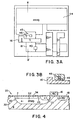
Fig. 1 is a top view of a prior art pinned photodiode based active pixel sensor (APS and PPS); -
Fig. 2 is a cross sectional view of the prior art APS and PPS shown inFig. 1 , taken through AA'; -
Fig. 3A is a top view of an APS and PPS sensor as envisioned by the present invention; -
Fig. 3B is a top view of an APS and PPS sensor similar to that shown inFig. 3A with a smaller unpinned region; -
Fig. 3C is a top view of a Passive Pixel Sensor as envisioned by the present invention; -
Fig. 4 is a cross sectional view of the APS and PPS shown inFig. 3A , taken through line BB'; -
Fig. 5A illustrates the prior art pinned photodiode based sensor as shown inFig. 2 ; -
Fig. 5B illustrates the electrostatic potential of the prior art pinned photodiode ofFig. 5A as seen along the line CC'; -
Fig. 6A is a cross section of the prior art photodiode shown in; -
Fig. 6B is a cross section of a partially pinned photodiode shown inFig. 4 ; -
Fig. 6C illustrates the electrostatic potential of the prior art photodiode seen along the line DD' ofFig. 6A ; -
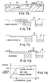
Fig. 7A is the cross section of the partially pinned photodiode based pixel as shown inFig. 4 ; -
Fig. 7B is an electrostatic potential diagram illustrating the operation of the pixel ofFig. 7A withinlinear region 1; -
Fig. 7C is an electrostatic potential diagram illustrating the operation of the pixel ofFig. 7A withinlinear region 2; -
Fig. 7D is an electrostatic potential diagram illustrating blooming of the pixel ofFig. 7A ; -
Fig. 7E is a diagram illustrating output voltage versus illumination level of the pixel shown inFig. 7A ; -
Fig. 8A is a cross sectional diagram of the partially pinned photodiode based pixel as shown inFig. 4 ; -
Fig. 8B is an electrostatic potential diagram illustrating the base reset level of the pixel ofFig. 8A ; -
Fig. 8C is an electrostatic potential diagram illustrating a first optional reset level of the pixel ofFig. 8A ; -
Fig. 8D is an electrostatic potential diagram illustrating a second optional reset level of the pixel ofFig. 8A ; -
Fig. 8E is a graph of the pixel output signal versus illumination level; -
Fig. 9A is cross sectional diagram of the partially pinned photodiode shown inFig. 4 with a corresponding electrostatic potential; -
Fig. 9B is a cross sectional diagram of a partially pinned photodiode with multiple implants to generate an electric field with a corresponding electrostatic illustrating an electric field built to assist in fast reset employing a staircase effect; -
Fig. 9C is a top view of a partially pinned photodiode having tapered implants or tapering active area; and -
Fig. 9D is a cross sectional diagram of a partially pinned photodiode ofFig. 9C with a corresponding electrostatic illustrating an electric field built to assist in fast reset employing a staircase effect. - To facilitate understanding, identical reference numerals have been used, where possible, to designate identical elements that are common to the figures.
- We have discovered that fill factors and other advantageous features can be improved within a pinned photodiode based active pixel sensor (APS and PPS) by pinning only a portion of the photodiode. The pinned photodiode has many desirable features, however, conventional pinned photodiodes have been unable to provide large fill factors.
- Referring to
Fig. 1 , which a top view of a prior artactive pixel 5 having a pinnedphotodiode 10 in conjunction withFig. 2 , which is a cross section ofFig. 1 through the line labeled AA', the region of interest in the prior art pinnedphotodiode APS pixel 5 is illustrated.Pixel 5, is formed upon a p-type substrate 20 with a pinnedphotodiode 10, atransfer gate 12, floatingdiffusion 14, resetgate 16, and areset drain 18. The pinnedphotodiode 10 comprises a lightly doped n-type region 22 within p-type substrate 20 and p-type pinning layer 24. As clearly seen inFig. 1 , a large portion of the area withinpixel 5 is used up by other features and not left for the pinnedphotodiode 10. - The pixel as shown in
Fig. 1 is disclosed by Lee et al. in allowedU.S. Patent Application 08/421,173 and provides low dark current, good blue quantum efficiency, and no image lag. Low dark current is achieved by using an appropriate dose and species of n-type photodiode implant so that all of the implant damage can be annealed with process times and temperatures that are compatible with the rest of the CMOS fabrication process requirements. Additionally low dark current is achieved by providing a p-type layer 24 at thesurface 19 that pins the potential of thesurface 19 to the potential of the substrate, typically the ground level or 0 volts. This suppresses dark current generation of interface states. Dark current suppression provides improvement in the signal to noise ratio of the photodetector by making the noise electron generation rate a smaller fraction of the photo-electron generation rate. - The fill factor of the pinned photodiode pixel, shown in
Fig. 1 , is defined as the percentage of the total pixel area that is the photodetector, is less than that typically provided by standard photodiode pixels. This is due to the addition of atransfer gate 12, floatingdiffusion 14 and associated metal interconnect (not shown). Although inclusion of these structures produces a no image lag, high conversion gain device, these structures occupy surface area that could otherwise be utilized as the photodetector. As a result the fill factor of a pinned photodiode pixel can be as much as two times less than that of a standard photodiode pixel, thus potentially adversely affecting the sensitivity of the device. - The APS pixel as envisioned by the present invention can be seen in
Fig. 3A. Fig. 4 is a cross sectional view ofFig. 3A through line BB'. These views illustrate the increase in fill factor achieved by the present invention, which is a result of the partially pinned photodiode architecture. Thenew pixel 35 comprises aphotodiode 30, formed insubstrate 20. It should be noted that thesubstrate 20 used with the present invention is the same substrate type as used with the prior art pinned photodiode previously discussed. However,pixel 35 of the present invention employs both a pinnedregion 44 and anun-pinned region 45, a combination which is undisclosed by prior art pinned photodiodes. Pinnedregion 44 is formed by an n-type implant to form n-type region 32 with a p-type pinning layer 34 formed on top of it. N-type region 37 is formed betweenreset gate 16 and pinnedregion 44 such that it is within the unpinnedregion 45.Contact 46 is formed on top of n-type region 37 to provide for the sensing of stored charge fromphotodiode 30. Additionally, areset gate 16, and areset drain 18 are provided within the preferred embodiment of the present invention to drain any undesired charge and provide reset of thepixel 35. It will be understood by those skilled in the art that a vertical overflow drain (VOD), not shown, could also be used to provide reset of thepixel 35. A top view of thispixel 35 is shown inFig. 3A , where it is apparent that an appreciable portion of the photo-sensitive region is encompassed by pinnedregion 44, with a relatively small area being allotted to unpinnedregion 45. Thispixel 35 substantially retains the advantages of the prior art pinned photodiode pixel. These advantages include low dark current and good blue quantum efficiency. Thepixel 35 of the present invention has no transfer gate and lacks a dedicated floating diffusion. Instead the unpinnedregion 45 is a floating region near the surface ofpixel 35. Since unpinnedregion 45 is floating, it functions in a manner similar to the floating diffusion illustrated within the prior art pixel. - Referring to
Fig. 3B , which is a top view of an APS sensor similar to that shown inFig. 3A with asmaller unpinned region 45, and advantages of less image lag due to lower capacitance of theunpinned region 45. However, the APS sensor ofFig. 3A has a higher sensitivity due to the larger unpinnedregion 45 which has a smaller capacitance than the pinnedregion 44. This will be described in further detail below. -
Fig. 3C is a top view of a Passive Pixel Sensor, generally referred to as 50, as envisioned by the present invention. Passive pixel sensors refers to those sensors that do not contain signal amplification means within the pixel, but instead, typically contain passive elements. Passive pixel sensors typically have the photodetector and a switch to connect the photodetector to a signal bus. Theunpinned region 55 can function as an integral part of a passive element which could be: a resistor; a capacitor; or a transistor used as a switch. The partially pinned photodiode comprising pinnedregion 54 and unpinnedregion 55 functions as the photodetector with theunpinned region 55 being operatively connected to the passive elements.Select gate 57 provides for selection of the pixel and drain 59 removes any undesired stored charge. -
Fig. 5B is an illustration of the electrostatic potential profile of the prior art pinnedphotodiode 10 based APS shown inFig. 5A along the line C-C'. Pinning the surface potential of the photodiode also improves blue quantum efficiency by providing an electric field that pulls photo-electrons generated at the surface into the electrostatic potential well of the pinnedphotodiode 10. This is depicted inFig. 5B . Blue quantum efficiency is also improved by reducing the recombination of shallow photo-electrons through suppression of interface states. Image lag is eliminated by providing a completely depleted pinnedphotodiode 10 structure, with an electrostatic potential that is shallower than the "on" potential of thetransfer gate 12, so that all of the photo-electrons are transferred to the floatingdiffusion region 14 without entering a sub-threshold regime, by turning on thetransfer gate 12. - Image lag in photodiode APS and PPS devices is explained in the following discussion. The electrostatic potential along line D-D' of the standard photodiode in
Fig. 6A is shown inFig. 6C . In APS and PPS devices, it is desirable to have all of the timing and signal levels to be the same as the CMOS logic levels, (i.e. 0V and 5V, or 0V and 3.3V). It is also desirable to have the reset drain voltage (Vrd) at a level that will maximize the diode signal swing and charge capacity. Therefore, Vrd, is kept as deep as possible by applying the highest potential for the CMOS device, typically this would be the supplied power source (Vdd). - Given these constraints (reset gate on-voltage and Vrd remaining at a potential equal to the CMOS Vdd), it is not possible to make the electrostatic potential of the reset gate as deep as that of the reset drain. This is depicted in
Fig. 6C . As a result, in order for the photodiode to be completely reset to the level of the reset drain, the remaining electrons must be removed by subthreshold current. As the photodiode gets reset closer to the level of the reset drain potential, the ΔV as shown inFig. 6C gets progressively smaller. Since the subthreshold current is proportional to eΔV as ΔV gets smaller, the subthreshold current gets smaller. It is evident that the photodiode cannot be completely reset in a short period of time. Consequently, if a bright image from a previous frame coincides with a dark image from the present frame, the residual charge from the incomplete reset in the previous frame will be read out and interpreted as signal charge in the present dark area, thus producing a "ghost" image effect. This is an objectionable image artifact in many imaging applications. This problem can be overcome by utilizing a depletion mode reset gate, or by setting Vrd to a lower voltage. However, this also leads to a lower signal swing and charge capacity which is not desirable. - Although image lag is not entirely eliminated in the partially pinned photodiode pixel, it is substantially less than that produced by a standard photodiode pixel. As shown in
Fig. 6B , this is attributable to a smaller capacitance, Cpppd associated with the un-pinned signal charge storage region in the partially pinned photodiode pixel, compared to that of the photodiode pixel. This capacitance is smaller due to the smaller unpinnedregion 45 for the device shown inFig. 6B as compared to the device shown inFig. 6A . The source implant resulting inunpinned region 45 is typically shallower than the more lightly doped photodiode implant. This capacitance can be minimized in the partially pinnedphotodiode 30 by making theunpinned region 45 as small as possible by using self alignment techniques that are well known in semiconductor processing. This is depicted inFig. 3B . The size of thisun-pinned region 45 can be designed to provide the desired lag and linear sensitivity range oflinear region 1 as shown inFig. 7E . Given the same reset gate voltage level, it will take less time to remove the photogenerated electrons from the partially pinned photodiode pixel compared to the standard photodiode pixel. Hence a partially pinned photodiode will have less image lag, (fewer number of electrons left in the photodetector after the reset operation), and can be reset in less time, enabling faster operation. - The partially pinned photodiode based pixel architecture has a fill factor comparable to that of the standard photodiode. Given the same design rules used to layout the pinned photodiode pixel, the fill factor of the partially pinned photodiode can be as much as 2 times larger than the pinned photodiode pixel. This is due to the elimination of the transfer gate and floating diffusion areas, and associated interconnect.
- The fill factor advantage of the partially pinned photodiode compared to that of the pinned photodiode is even more evident when viewed with respect to anti-blooming control. Both the pinned and partially pinned photodiode can provide anti-blooming by appropriately biasing the transfer gate or reset gate during integration, to drain away excess photoelectrons. However, in order to provide a means for anti-blooming control for extremely high light levels that could fill up the photodetector during readout of the photodetector, the pinned photodiode pixel must have a separate overflow drain. This could be either a lateral overflow drain and gate, or a vertical overflow drain structure. The lateral overflow drain and gate consumes more photodetector area, thus further reducing the fill factor. Implementation of a vertical overflow drain structure requires additional process steps, increasing process complexity and cost.
- With the partially pinned photodiode pixel, anti-blooming control for extremely high light levels can be accomplished without an added overflow drain. The reset drain functions as the overflow drain for the partially pinned photodiode. The level of anti-blooming can be controlled by appropriately controlling the potential of the reset gate. In the case where it is desired to have only a 2-level signal applied to the reset gate, (i.e. on and off), a buried channel reset gate can be employed to set the off potential of the reset gate at an appropriate level that is deeper than zero volts. Alternately, the level of anti-blooming can be controlled by applying the appropriate reset gate voltage, (an intermediate level in between the on and off voltage). This could be done with a surface channel or buried channel reset gate. It should also be noted that a buried channel reset gate eliminates image lag.
- This approach to anti-blooming control in a photodiode, pinned photodiode, or partially pinned
photodiode pixel 30 has the disadvantage of reducing the charge capacity of the photodetector. This is due to the fact that anti-blooming control is achieved by lowering the electrostatic potential barrier to electrons between the photodetector and theoverflow reset drain 18. The partially pinnedphotodiode pixel 30 has the advantage of being able to incorporate anti-blooming control without reducing the charge capacity of the detector. This is depicted inFig. 7A-E . The level of anti-blooming protection is typically defined as the ratio of the light level required to produce blooming, (to fill up the entire photodetector in the case of APS and PPS), compared to the light level required to reach the maximum signal in the linear region of the photodetector, (saturation signal or Vsat). For the case where anoverflow reset drain 18 is utilized, the level of anti-blooming protection is determined by the resistance of the region between the photodetector and theoverflow reset drain 18. For the partially pinnedphotodiode 30 the electrostatic potential of the reset gate can be left at zero volts and achieve anti-blooming by designing the size of theun-pinned region 45 to provide the desired Vsat. As long as the number of photo-generated electrons is less than or equal to the capacity of theun-pinned region 45, they will all reside in theun-pinned region 45 and produce thelinear transfer function 1 shown inFig. 7B and 7E . As the number of electrons exceed the capacity of theun-pinned region 45, the pinnedregion 44 begins to fill up with electrons, as shown inFig. 7C . Since the pinnedregion 44 has a higher capacitance than theun-pinned region 45, this will produce a secondlinear transfer function 2 as shown inFig. 7E . This will continue until the capacity of the pinnedregion 44 is exceeded, and then electrons will begin to spill over thereset gate 16 into thereset drain 18 or from the diode into other regions of the pixel, (i.e. blooming begins to occur). This is shown inFigs. 7D and 7E . The level of anti-blooming control, ABX = B/A, is determined and set by the design of the pinned and un-pinned regions. This is also shown inFig. 7E . It is evident that anti-blooming control is achieved without lowering the electrostatic barrier between the photodetector and the reset drain, thus providing anti-blooming control without sacrificing charge capacity. -
Figure 8A is a cross sectional diagram of the partially pinned photodiode based pixel as shown inFig. 4 .Figure 8B is an electrostatic potential diagram illustrating the base reset level of the pixel ofFig. 8A. Figure 8C is an electrostatic potential diagram illustrating a first optional reset level of the pixel ofFig. 8A. Fig. 8D is an electrostatic potential diagram illustrating a second optional reset level of the pixel ofFig. 8A. Figure 8E is a graph of the pixel output signal versus illumination level. The partially pinnedphotodiode 30 also provides dynamic range compression by utilizing the second linear transfer region. This is useful in scenes or images where there is a large range of brightness in the image and detail in both the low light and high light portions of the scene. Without this compression, all detail in the bright region would be lost due to being clipped at the saturation signal level. Control of the onset of the second linear transfer region can be done in two ways. The first method is by appropriately designing the size and capacitance of theun-pinned region 45 and the size and capacitance of the transistor that the diode is connected to (seeFig. 4 ). The second method consists of controlling thereset gate 16 signals so that thephotodiode 30 is reset to the desired level. These 2 methods can be used together. This is shown inFigures 8A through 8E with various reset levels determined byreset gate 16.Fig. 8E gives a graphical analysis of reset levels interim of the output signal versus the illumination level. - In order to provide fast reset rates it is also necessary to ensure quick transit of any photoelectrons that reside in the pinned
region 44 of the photodiode onto theun-pinned region 45. One method of doing this is to build in an electric field that will force them into the un-pinned region. This is normally not the case. The electrostatic potential of pinned region is a constant. This is shown inFig. 9A . The electric field can be produced in several ways. One way is to provide separate n-type or p-type implants that are offset to produce a staircase effect as shown inFig. 9B . Another method is to taper the existing n-photodiode implant, p-type pinning layer implant, or any additional n or p-type implants to cause a 2-dimensional modulation of the electrostatic potential. One of these is shown inFig. 9C . Another method is to taper the active area of the photodiode to produce a similar effect, as shown inFig. 9 . - The invention has been described with reference to a preferred embodiment; however, it will be appreciated that variations and modifications can be effected by a person of ordinary skill in the art without departing from the scope of the invention as defined in the appended claims.
-
- 5
- prior art pixel
- 10
- pinned photodiode
- 12
- transfer gate
- 14
- floating diffusion
- 16
- reset gate
- 18
- reset drain
- 19
- surface of substrate
- 20
- substrate
- 22
- lightly doped n-type region
- 24
- p-type pinning layer
- 30
- photodiode
- 32
- n-type implant for photodiode
- 34
- p-type pinning layer for partially pinned photodiode
- 35
- pixel of the present invention
- 37
- n-type floating region
- 44
- pinned region of partially pinned photodiode
- 45
- unpinned region of partially pinned photodiode
- 46
- contact
- 50
- passive pixel sensor
- 54
- pinned region
- 55
- unpinned region
- 57
- select gate
- 59
- drain
Claims (5)
- An image sensor having at least one pixel comprising:a semiconductor substrate (20) of a first conductivity type within the sensor, the semiconductor substrate (20) being formed on a surface of the sensor;at least one partially-pinned photodiode (30) formed, within the semiconductor substrate (20) at its surface, the partially-pinned photodiode (30) being formed by a second region (32) of a second conductivity type opposite the first conductivity type; wherein the partially-pinned photodiode (30) includesa pinning layer (34) of the first conductivity type formed at a surface of the second region (32) and over a portion of the second region (32) creating a pinned photodiode region (44); andan unpinned region (45) formed at the surface of the second region (32) in an area outside the portion used to form the pinning layer (34); and a sensing node coupled to the unpinned region interfacing the photodiode to external circuitry ; characterized in thatthe unpinned region (45) includes a floating region (37) comprising a third region of the second conductivity type formed at the surface of the unpinned region (45) and having a dopant concentration higher than that of the second region (32), wherein said sensing node comprises a contact (46) connected to the floating region (37), to provide for the sensing of stored charge from the photodiode.
- The image sensor of claim 1 further comprising reset means (16) for removing charge from the photodiode portion to a drain area (18).
- The image sensor of claim 1 wherein the sensor is an active pixel sensor.
- The image sensor of claim 1 wherein the pinned photodiode region (44) further comprises a gradient dopant level formed to create an electrostatic gradient capable of pushing electrons towards the unpinned region (45).
- A method of making an image sensor comprising the steps of:forming at least one partially-pinned photodiode (30) within a semiconductor substrate (20) of a first conductivity type at a surface of the semiconductor substrate (20), wherein the step of forming the partially-pinned photodiode (30) comprises the steps of forming a second region (32) of a second conductivity type opposite the first conductivity type at the surface of the semiconductor substrate (20);forming a pinning layer (34) of the first conductivity type at a surface of the second region (32) and over a portion of the second region (32) creating a pinned photodiode region (44) andan unpinned region (45), wherein the unpinned region (45) is formed at the surface of the second region (32) in an area outside the portion used to form the pinning layer (34); forming a floating region of a second conductivity type at a surface of the unpinned region (45), wherein the dopant concentration in the floating region (37) is higher than the dopant concentration in the second region (32) ; and forming a sensing node coupled to the unpinned region interfacing the photodiode to external circuitry, wherein said sensing node comprises a contact (46) connected to the floating region (37), to provide for the sensing of stored charge from the photodiode.
Applications Claiming Priority (2)
| Application Number | Priority Date | Filing Date | Title |
|---|---|---|---|
| US08/785,555 US5903021A (en) | 1997-01-17 | 1997-01-17 | Partially pinned photodiode for solid state image sensors |
| US785555 | 1997-01-17 |
Publications (3)
| Publication Number | Publication Date |
|---|---|
| EP0854516A2 EP0854516A2 (en) | 1998-07-22 |
| EP0854516A3 EP0854516A3 (en) | 1998-10-07 |
| EP0854516B1 true EP0854516B1 (en) | 2010-11-17 |
Family
ID=25135878
Family Applications (1)
| Application Number | Title | Priority Date | Filing Date |
|---|---|---|---|
| EP98200030A Expired - Lifetime EP0854516B1 (en) | 1997-01-17 | 1998-01-08 | Partially pinned photodiode for solid state image sensors |
Country Status (4)
| Country | Link |
|---|---|
| US (2) | US5903021A (en) |
| EP (1) | EP0854516B1 (en) |
| JP (1) | JPH10209422A (en) |
| DE (1) | DE69841998D1 (en) |
Families Citing this family (116)
| Publication number | Priority date | Publication date | Assignee | Title |
|---|---|---|---|---|
| US5625210A (en) * | 1995-04-13 | 1997-04-29 | Eastman Kodak Company | Active pixel sensor integrated with a pinned photodiode |
| US7199410B2 (en) * | 1999-12-14 | 2007-04-03 | Cypress Semiconductor Corporation (Belgium) Bvba | Pixel structure with improved charge transfer |
| US6815791B1 (en) | 1997-02-10 | 2004-11-09 | Fillfactory | Buried, fully depletable, high fill factor photodiodes |
| JPH10270742A (en) * | 1997-03-28 | 1998-10-09 | Rohm Co Ltd | Photodiode |
| US6026964A (en) * | 1997-08-25 | 2000-02-22 | International Business Machines Corporation | Active pixel sensor cell and method of using |
| JPH11126893A (en) * | 1997-10-23 | 1999-05-11 | Nikon Corp | Solid-state image-pickup element and manufacture thereof |
| US6714239B2 (en) * | 1997-10-29 | 2004-03-30 | Eastman Kodak Company | Active pixel sensor with programmable color balance |
| US6127697A (en) * | 1997-11-14 | 2000-10-03 | Eastman Kodak Company | CMOS image sensor |
| JP3874135B2 (en) * | 1997-12-05 | 2007-01-31 | 株式会社ニコン | Solid-state image sensor |
| NL1011381C2 (en) * | 1998-02-28 | 2000-02-15 | Hyundai Electronics Ind | Photodiode for a CMOS image sensor and method for its manufacture. |
| JPH11264761A (en) * | 1998-03-18 | 1999-09-28 | Honda Motor Co Ltd | Optical sensor circuit and image sensor using the same |
| TW425563B (en) * | 1998-06-03 | 2001-03-11 | Nippon Electric Co | Solid state image pickup device and driving method therefore |
| US6410899B1 (en) | 1998-06-17 | 2002-06-25 | Foveon, Inc. | Active pixel sensor with bootstrap amplification and reduced leakage during readout |
| US6512544B1 (en) * | 1998-06-17 | 2003-01-28 | Foveon, Inc. | Storage pixel sensor and array with compression |
| US6259145B1 (en) * | 1998-06-17 | 2001-07-10 | Intel Corporation | Reduced leakage trench isolation |
| JP2000082839A (en) * | 1998-06-29 | 2000-03-21 | Hyundai Electronics Ind Co Ltd | Photodiode, unit pixel of image sensor provided therewith, and method of obtaining data therefrom |
| FR2781929B1 (en) * | 1998-07-28 | 2002-08-30 | St Microelectronics Sa | IMAGE SENSOR WITH PHOTODIODE ARRAY |
| US6259124B1 (en) * | 1998-08-07 | 2001-07-10 | Eastman Kodak Company | Active pixel sensor with high fill factor blooming protection |
| US6677628B2 (en) * | 1998-09-17 | 2004-01-13 | Micron Technology, Inc. | Pinned floating photoreceptor with active pixel sensor |
| US7015964B1 (en) | 1998-11-02 | 2006-03-21 | Canon Kabushiki Kaisha | Solid-state image pickup device and method of resetting the same |
| US6207984B1 (en) * | 1998-12-23 | 2001-03-27 | United Microelectronics Corp. | CMOS sensor |
| US6232626B1 (en) * | 1999-02-01 | 2001-05-15 | Micron Technology, Inc. | Trench photosensor for a CMOS imager |
| US20030089929A1 (en) * | 2001-02-14 | 2003-05-15 | Rhodes Howard E. | Trench photosensor for a CMOS imager |
| ATE310319T1 (en) * | 1999-02-05 | 2005-12-15 | Omnivision Tech Inc | METHOD OF PRODUCING AN ACTIVE PIXEL IMAGE SENSOR HAVING A MOUNTING LAYER TYPE PHOTODIODE |
| TW484235B (en) * | 1999-02-25 | 2002-04-21 | Canon Kk | Light-receiving element and photoelectric conversion device |
| WO2000052765A1 (en) * | 1999-03-01 | 2000-09-08 | Photobit Corporation | Active pixel sensor with fully-depleted buried photoreceptor |
| JP3576033B2 (en) * | 1999-03-31 | 2004-10-13 | 株式会社東芝 | Solid-state imaging device |
| US6476426B1 (en) | 1999-07-06 | 2002-11-05 | Motorola, Inc. | Electronic component and method for improving pixel charge transfer in the electronic component |
| US6697114B1 (en) | 1999-08-13 | 2004-02-24 | Foveon, Inc. | Triple slope pixel sensor and arry |
| US6300219B1 (en) | 1999-08-30 | 2001-10-09 | Micron Technology, Inc. | Method of forming trench isolation regions |
| US6090639A (en) * | 1999-09-08 | 2000-07-18 | United Microelectronics Corp. | Method for forming a photo diode and a CMOS transistor simultaneously |
| US6271553B1 (en) * | 1999-11-29 | 2001-08-07 | United Microelectronics Corp. | Photo sensor in a photo diode |
| JP4419238B2 (en) * | 1999-12-27 | 2010-02-24 | ソニー株式会社 | Solid-state imaging device and manufacturing method thereof |
| US6710804B1 (en) * | 2000-01-18 | 2004-03-23 | Eastman Kodak Company | CMOS active pixel image sensor with extended dynamic range and sensitivity |
| US6809768B1 (en) | 2000-02-14 | 2004-10-26 | Foveon, Inc. | Double slope pixel sensor and array |
| US6882367B1 (en) | 2000-02-29 | 2005-04-19 | Foveon, Inc. | High-sensitivity storage pixel sensor having auto-exposure detection |
| US6372537B1 (en) * | 2000-03-17 | 2002-04-16 | Taiwan Semiconductor Manufacturing Company | Pinned photodiode structure in a 3T active pixel sensor |
| US6518085B1 (en) * | 2000-08-09 | 2003-02-11 | Taiwan Semiconductor Manufacturing Company | Method for making spectrally efficient photodiode structures for CMOS color imagers |
| US6448596B1 (en) * | 2000-08-15 | 2002-09-10 | Innotech Corporation | Solid-state imaging device |
| US6365926B1 (en) * | 2000-09-20 | 2002-04-02 | Eastman Kodak Company | CMOS active pixel with scavenging diode |
| WO2002027763A2 (en) | 2000-09-25 | 2002-04-04 | Foveon, Inc. | Active pixel sensor with noise cancellation |
| JP2002151729A (en) * | 2000-11-13 | 2002-05-24 | Sony Corp | Semiconductor device and its manufacturing method |
| US6566697B1 (en) | 2000-11-28 | 2003-05-20 | Dalsa, Inc. | Pinned photodiode five transistor pixel |
| US6504195B2 (en) * | 2000-12-29 | 2003-01-07 | Eastman Kodak Company | Alternate method for photodiode formation in CMOS image sensors |
| JP3724374B2 (en) | 2001-01-15 | 2005-12-07 | ソニー株式会社 | Solid-state imaging device and driving method thereof |
| JP4130307B2 (en) * | 2001-01-15 | 2008-08-06 | Necエレクトロニクス株式会社 | Solid-state imaging device |
| US6713796B1 (en) | 2001-01-19 | 2004-03-30 | Dalsa, Inc. | Isolated photodiode |
| FR2820882B1 (en) * | 2001-02-12 | 2003-06-13 | St Microelectronics Sa | THREE TRANSISTOR PHOTODETECTOR |
| FR2820883B1 (en) * | 2001-02-12 | 2003-06-13 | St Microelectronics Sa | HIGH CAPACITY PHOTODIODE |
| US7180798B2 (en) * | 2001-04-12 | 2007-02-20 | Fuji Electric Co., Ltd. | Semiconductor physical quantity sensing device |
| FR2824665B1 (en) * | 2001-05-09 | 2004-07-23 | St Microelectronics Sa | CMOS TYPE PHOTODETECTOR |
| KR100381026B1 (en) * | 2001-05-22 | 2003-04-23 | 주식회사 하이닉스반도체 | CMOS Image sensor capable of increasing punch through voltage and charge integration of photodiode and method for forming the same |
| JP2003060192A (en) * | 2001-08-20 | 2003-02-28 | Sony Corp | Method for manufacturing solid-state image pickup device |
| US6881986B1 (en) | 2001-11-07 | 2005-04-19 | Taiwan Semiconductor Manufacturing Company | Design and fabrication method for finger n-type doped photodiodes with high sensitivity for CIS products |
| FR2833408B1 (en) * | 2001-12-12 | 2004-03-12 | St Microelectronics Sa | METHOD FOR CONTROLLING THE ILLUMINATION OF A PHOTODIODE AND CORRESPONDING INTEGRATED CIRCUIT |
| JP2003258231A (en) * | 2002-03-05 | 2003-09-12 | Sony Corp | Solid-state image sensor |
| KR20030096659A (en) * | 2002-06-17 | 2003-12-31 | 삼성전자주식회사 | Pixel array region of an image sensor, structure thereof and fabrication method thereof |
| US6781171B2 (en) * | 2002-07-19 | 2004-08-24 | Dongbu Electronics Co., Ltd. | Pinned photodiode for a CMOS image sensor and fabricating method thereof |
| US6744084B2 (en) * | 2002-08-29 | 2004-06-01 | Micro Technology, Inc. | Two-transistor pixel with buried reset channel and method of formation |
| JP2005537654A (en) * | 2002-08-30 | 2005-12-08 | コーニンクレッカ フィリップス エレクトロニクス エヌ ヴィ | Image sensor, camera system provided with image sensor, and method of manufacturing such apparatus |
| US6586789B1 (en) * | 2002-10-07 | 2003-07-01 | Lixin Zhao | Pixel image sensor |
| US7087944B2 (en) * | 2003-01-16 | 2006-08-08 | Micron Technology, Inc. | Image sensor having a charge storage region provided within an implant region |
| EP1465258A1 (en) * | 2003-02-21 | 2004-10-06 | STMicroelectronics Limited | CMOS image sensors |
| KR20040093786A (en) * | 2003-04-30 | 2004-11-09 | 매그나칩 반도체 유한회사 | Method of manufacturing cmos image sensor |
| US7009227B2 (en) * | 2003-06-16 | 2006-03-07 | Micron Technology, Inc. | Photodiode structure and image pixel structure |
| FR2857158B1 (en) * | 2003-07-01 | 2006-04-28 | St Microelectronics Sa | METHOD FOR CONTROLLING A MOS TYPE PHOTOCOPIER |
| US6900484B2 (en) * | 2003-07-30 | 2005-05-31 | Micron Technology, Inc. | Angled pinned photodiode for high quantum efficiency |
| US7115855B2 (en) * | 2003-09-05 | 2006-10-03 | Micron Technology, Inc. | Image sensor having pinned floating diffusion diode |
| US7541627B2 (en) * | 2004-03-08 | 2009-06-02 | Foveon, Inc. | Method and apparatus for improving sensitivity in vertical color CMOS image sensors |
| US7238977B2 (en) * | 2004-08-19 | 2007-07-03 | Micron Technology, Inc. | Wide dynamic range sensor having a pinned diode with multiple pinned voltages |
| US7492404B2 (en) * | 2004-08-27 | 2009-02-17 | Eastman Kodak Company | Fast flush structure for solid-state image sensors |
| JP4756839B2 (en) | 2004-09-01 | 2011-08-24 | キヤノン株式会社 | Solid-state imaging device and camera |
| KR100614650B1 (en) * | 2004-09-16 | 2006-08-22 | 삼성전자주식회사 | Image sensor and method for forming the same |
| JP4613305B2 (en) | 2004-10-19 | 2011-01-19 | 国立大学法人静岡大学 | Imaging device with embedded photodiode structure |
| KR20060058573A (en) * | 2004-11-25 | 2006-05-30 | 한국전자통신연구원 | Cmos image sensor |
| JP4725095B2 (en) | 2004-12-15 | 2011-07-13 | ソニー株式会社 | Back-illuminated solid-state imaging device and manufacturing method thereof |
| KR100654342B1 (en) * | 2005-02-07 | 2006-12-08 | 삼성전자주식회사 | image sensor |
| US7701493B2 (en) * | 2005-02-28 | 2010-04-20 | Micron Technology, Inc. | Imager row-wise noise correction |
| US7750958B1 (en) | 2005-03-28 | 2010-07-06 | Cypress Semiconductor Corporation | Pixel structure |
| US7808022B1 (en) | 2005-03-28 | 2010-10-05 | Cypress Semiconductor Corporation | Cross talk reduction |
| EP2249387B1 (en) | 2005-03-28 | 2012-09-05 | Fujitsu Semiconductor Limited | Imaging device |
| TWI266429B (en) * | 2005-05-05 | 2006-11-11 | Pixart Imaging Inc | Pinned photodiode sensor with gate controlled SCR transfer switch and method of formation |
| US20070023803A1 (en) * | 2005-07-26 | 2007-02-01 | Dongbu Electronics Co., Ltd. | CMOS image sensor and method of fabricating the same |
| KR100752182B1 (en) * | 2005-10-12 | 2007-08-24 | 동부일렉트로닉스 주식회사 | CMOS image sensor and method for manufacturing the same |
| US7682977B2 (en) * | 2006-05-11 | 2010-03-23 | Micron Technology, Inc. | Methods of forming trench isolation and methods of forming arrays of FLASH memory cells |
| KR100738516B1 (en) | 2006-05-25 | 2007-07-11 | (주) 픽셀플러스 | Active pixel having pinned photodiode with coupling capacitor and method for sensing a signal thereof |
| KR100790587B1 (en) * | 2006-05-25 | 2008-01-02 | (주) 픽셀플러스 | Image sensor pixel having pinned photodiode with coupling capacitor and method for sensing a signal thereof |
| US7675093B2 (en) * | 2006-11-28 | 2010-03-09 | Micron Technology, Inc. | Antiblooming imaging apparatus, system, and methods |
| US8304821B2 (en) * | 2006-12-23 | 2012-11-06 | Semiconductor Manufacturing International (Shanghai) Corporation | CMOS image sensor |
| JP5584982B2 (en) * | 2009-02-09 | 2014-09-10 | ソニー株式会社 | Solid-state imaging device and camera system |
| US7724293B2 (en) * | 2007-03-12 | 2010-05-25 | Aptina Imaging Corporation | Multi-purpose image sensor circuits, imager, system and method of operation |
| US7915702B2 (en) * | 2007-03-15 | 2011-03-29 | Eastman Kodak Company | Reduced pixel area image sensor |
| US7834411B2 (en) * | 2007-05-15 | 2010-11-16 | Foveon, Inc. | CMOS pixel sensor with depleted photocollectors and a depleted common node |
| US7763837B2 (en) * | 2007-11-20 | 2010-07-27 | Aptina Imaging Corporation | Method and apparatus for controlling anti-blooming timing to reduce effects of dark current |
| CN101459184B (en) * | 2007-12-13 | 2011-03-23 | 中芯国际集成电路制造(上海)有限公司 | System and method for sensing image on CMOS |
| CN101625996B (en) * | 2008-07-08 | 2011-03-23 | 中芯国际集成电路制造(上海)有限公司 | ONO side wall etching process for reducing dark current |
| CN101630659B (en) * | 2008-07-15 | 2012-05-23 | 中芯国际集成电路制造(上海)有限公司 | Method for forming CMOS image sensor by using tri-gate process and structure of CMOS image sensor using tri-gate process |
| JP5283216B2 (en) * | 2008-07-31 | 2013-09-04 | 国立大学法人静岡大学 | High-speed charge transfer photodiode, lock-in pixel and solid-state imaging device |
| US8476567B2 (en) | 2008-09-22 | 2013-07-02 | Semiconductor Components Industries, Llc | Active pixel with precharging circuit |
| US8329499B2 (en) * | 2008-12-10 | 2012-12-11 | Truesense Imaging, Inc. | Method of forming lateral overflow drain and channel stop regions in image sensors |
| WO2010074252A1 (en) * | 2008-12-25 | 2010-07-01 | 国立大学法人静岡大学 | Semiconductor device and solid-state imaging device |
| JP5493430B2 (en) | 2009-03-31 | 2014-05-14 | ソニー株式会社 | SOLID-STATE IMAGING DEVICE, ITS MANUFACTURING METHOD, AND ELECTRONIC DEVICE |
| DE102009020218B8 (en) * | 2009-05-07 | 2011-05-12 | Fraunhofer-Gesellschaft zur Förderung der angewandten Forschung e.V. | Detector and method for detecting electromagnetic radiation and computer program for carrying out the method |
| WO2011043339A1 (en) * | 2009-10-05 | 2011-04-14 | 国立大学法人静岡大学 | Semiconductor element and solid-state imaging device |
| US8907388B2 (en) | 2010-02-05 | 2014-12-09 | National University Corporation Shizuoka University | Optical-information acquiring element, optical information acquiring element array, and hybrid solid-state imaging device |
| US8878264B2 (en) * | 2011-04-26 | 2014-11-04 | Aptina Imaging Corporation | Global shutter pixel with improved efficiency |
| DE102011076635B3 (en) * | 2011-05-27 | 2012-10-18 | Fraunhofer-Gesellschaft zur Förderung der angewandten Forschung e.V. | Photodetector i.e. lateral drift field photodetector, for detecting electromagnetic radiation, has bus control electrode arranged in region of trough adjacent to connection doping regions, transfer control electrodes and detection region |
| FR2986906B1 (en) | 2012-02-15 | 2015-06-19 | New Imaging Technologies Sas | IMPROVED LOAD TRANSFER ACTIVE PIXEL STRUCTURE |
| JP6077786B2 (en) | 2012-08-22 | 2017-02-08 | キヤノン株式会社 | Imaging device |
| FR2997596B1 (en) | 2012-10-26 | 2015-12-04 | New Imaging Technologies Sas | STRUCTURE OF A CMOS ACTIVE PIXEL |
| US9348035B2 (en) | 2013-10-22 | 2016-05-24 | General Electric Company | Systems and methods for selectable detector configurations |
| US9526468B2 (en) | 2014-09-09 | 2016-12-27 | General Electric Company | Multiple frame acquisition for exposure control in X-ray medical imagers |
| TWI731026B (en) | 2016-01-15 | 2021-06-21 | 新加坡商海特根微光學公司 | Semiconductor devices |
| US10236400B2 (en) | 2016-02-01 | 2019-03-19 | Heptagon Micro Optics Pte. Ltd. | Quantum dot film based demodulation structures |
| CN111095560A (en) * | 2017-11-30 | 2020-05-01 | 松下知识产权经营株式会社 | Image pickup apparatus |
| GB2574619B (en) | 2018-06-12 | 2022-10-12 | Res & Innovation Uk | Image sensor |
Citations (3)
| Publication number | Priority date | Publication date | Assignee | Title |
|---|---|---|---|---|
| US5051797A (en) * | 1989-09-05 | 1991-09-24 | Eastman Kodak Company | Charge-coupled device (CCD) imager and method of operation |
| US5262871A (en) * | 1989-11-13 | 1993-11-16 | Rutgers, The State University | Multiple resolution image sensor |
| US5514887A (en) * | 1993-12-09 | 1996-05-07 | Nec Corporation | Solid state image sensor having a high photoelectric conversion efficiency |
Family Cites Families (26)
| Publication number | Priority date | Publication date | Assignee | Title |
|---|---|---|---|---|
| JPS5651165A (en) * | 1979-10-03 | 1981-05-08 | Hitachi Ltd | Noise eliminating circuit |
| US4484210A (en) * | 1980-09-05 | 1984-11-20 | Nippon Electric Co., Ltd. | Solid-state imaging device having a reduced image lag |
| JPS57121374A (en) * | 1981-01-21 | 1982-07-28 | Hitachi Ltd | Solid image pickup device |
| JPH0714044B2 (en) * | 1984-11-22 | 1995-02-15 | 株式会社日立製作所 | Charge coupled device input circuit |
| JPS62160750A (en) * | 1986-01-10 | 1987-07-16 | Hitachi Ltd | Substrate-voltage generating circuit |
| JPS63100879A (en) * | 1986-10-17 | 1988-05-02 | Hitachi Ltd | Solid-state image pickup device |
| JPS63299268A (en) * | 1987-05-29 | 1988-12-06 | Toshiba Corp | Solid-state image sensing device |
| JPH01135184A (en) * | 1987-11-19 | 1989-05-26 | Nec Corp | Solid-state image pickup element |
| US4984047A (en) * | 1988-03-21 | 1991-01-08 | Eastman Kodak Company | Solid-state image sensor |
| US4908518A (en) * | 1989-02-10 | 1990-03-13 | Eastman Kodak Company | Interline transfer CCD image sensing device with electrode structure for each pixel |
| US5115458A (en) * | 1989-09-05 | 1992-05-19 | Eastman Kodak Company | Reducing dark current in charge coupled devices |
| US5182623A (en) * | 1989-11-13 | 1993-01-26 | Texas Instruments Incorporated | Charge coupled device/charge super sweep image system and method for making |
| JPH07105458B2 (en) * | 1989-11-21 | 1995-11-13 | 株式会社東芝 | Composite integrated circuit device |
| US5235198A (en) * | 1989-11-29 | 1993-08-10 | Eastman Kodak Company | Non-interlaced interline transfer CCD image sensing device with simplified electrode structure for each pixel |
| US5060245A (en) * | 1990-06-29 | 1991-10-22 | The United States Of America As Represented By The Secretary Of The Air Force | Interline transfer CCD image sensing apparatus |
| JP3125303B2 (en) * | 1990-11-26 | 2001-01-15 | 日本電気株式会社 | Solid-state imaging device |
| US5256891A (en) * | 1991-06-07 | 1993-10-26 | Eastman Kodak Company | CCD electrode structure for image sensors |
| EP0526993B1 (en) * | 1991-07-11 | 2000-09-27 | Texas Instruments Incorporated | Charge multiplying detector (CMD) suitable for small pixel CCD image sensors |
| JPH05251684A (en) * | 1991-11-25 | 1993-09-28 | Eastman Kodak Co | Ccd image sensor having improved bloom prevention characteristic |
| JPH05283666A (en) * | 1992-03-30 | 1993-10-29 | Sony Corp | Solid state image pickup |
| KR960002645B1 (en) * | 1992-04-03 | 1996-02-24 | 엘지반도체주식회사 | Charge transferring device and solid state image picking-up device |
| US5235196A (en) * | 1992-07-24 | 1993-08-10 | Eastman Kodak Company | Transfer region design for charge-coupled device image sensor |
| US5471515A (en) * | 1994-01-28 | 1995-11-28 | California Institute Of Technology | Active pixel sensor with intra-pixel charge transfer |
| KR0136934B1 (en) * | 1994-02-23 | 1998-04-24 | 문정환 | Linear ccd solid image sensor |
| US5514886A (en) * | 1995-01-18 | 1996-05-07 | Eastman Kodak Company | Image sensor with improved output region for superior charge transfer characteristics |
| US5625210A (en) * | 1995-04-13 | 1997-04-29 | Eastman Kodak Company | Active pixel sensor integrated with a pinned photodiode |
-
1997
- 1997-01-17 US US08/785,555 patent/US5903021A/en not_active Expired - Lifetime
-
1998
- 1998-01-08 EP EP98200030A patent/EP0854516B1/en not_active Expired - Lifetime
- 1998-01-08 DE DE69841998T patent/DE69841998D1/en not_active Expired - Lifetime
- 1998-01-16 JP JP10007072A patent/JPH10209422A/en active Pending
- 1998-10-01 US US09/164,968 patent/US6051447A/en not_active Expired - Lifetime
Patent Citations (3)
| Publication number | Priority date | Publication date | Assignee | Title |
|---|---|---|---|---|
| US5051797A (en) * | 1989-09-05 | 1991-09-24 | Eastman Kodak Company | Charge-coupled device (CCD) imager and method of operation |
| US5262871A (en) * | 1989-11-13 | 1993-11-16 | Rutgers, The State University | Multiple resolution image sensor |
| US5514887A (en) * | 1993-12-09 | 1996-05-07 | Nec Corporation | Solid state image sensor having a high photoelectric conversion efficiency |
Also Published As
| Publication number | Publication date |
|---|---|
| US6051447A (en) | 2000-04-18 |
| DE69841998D1 (en) | 2010-12-30 |
| EP0854516A2 (en) | 1998-07-22 |
| JPH10209422A (en) | 1998-08-07 |
| EP0854516A3 (en) | 1998-10-07 |
| US5903021A (en) | 1999-05-11 |
Similar Documents
| Publication | Publication Date | Title |
|---|---|---|
| EP0854516B1 (en) | Partially pinned photodiode for solid state image sensors | |
| US9654713B2 (en) | Image sensors, methods, and pixels with tri-level biased transfer gates | |
| EP2030240B1 (en) | Pmos pixel structure with low cross talk | |
| US6858460B2 (en) | Retrograde well structure for a CMOS imager | |
| USRE45357E1 (en) | Twin p-well CMOS imager | |
| US6278142B1 (en) | Semiconductor image intensifier | |
| US6815743B2 (en) | CMOS imager and method of formation | |
| JP3645585B2 (en) | Charge coupled device type solid-state imaging device having overflow drain structure | |
| US7687832B2 (en) | Method of fabricating a storage gate pixel design | |
| US7598132B2 (en) | Active photosensitive structure with buried depletion layer | |
| US6927089B2 (en) | CMOS imager and method of formation | |
| US5872371A (en) | Active pixel sensor with punch-through reset and cross-talk suppression | |
| US7265397B1 (en) | CCD imager constructed with CMOS fabrication techniques and back illuminated imager with improved light capture | |
| US20040051801A1 (en) | Solid-state image pickup device and device driving control method for solid-state image pickup | |
| US20080210996A1 (en) | Frame shutter pixel with an isolated storage node | |
| US8508638B2 (en) | 3T pixel for CMOS image sensors with low reset noise and low dark current generation utilizing parametric reset | |
| US6259124B1 (en) | Active pixel sensor with high fill factor blooming protection | |
| EP0809299B1 (en) | Active pixel sensor with punch-through reset and cross-talk suppression | |
| US20020163020A1 (en) | Retrograde well structure for a CMOS imager | |
| KR19990018938A (en) | Charge Coupled Image Sensor |
Legal Events
| Date | Code | Title | Description |
|---|---|---|---|
| PUAI | Public reference made under article 153(3) epc to a published international application that has entered the european phase |
Free format text: ORIGINAL CODE: 0009012 |
|
| AK | Designated contracting states |
Kind code of ref document: A2 Designated state(s): DE FR GB |
|
| AX | Request for extension of the european patent |
Free format text: AL;LT;LV;MK;RO;SI |
|
| PUAL | Search report despatched |
Free format text: ORIGINAL CODE: 0009013 |
|
| AK | Designated contracting states |
Kind code of ref document: A3 Designated state(s): AT BE CH DE DK ES FI FR GB GR IE IT LI LU MC NL PT SE |
|
| 17P | Request for examination filed |
Effective date: 19990308 |
|
| AKX | Designation fees paid |
Free format text: DE FR GB |
|
| GRAP | Despatch of communication of intention to grant a patent |
Free format text: ORIGINAL CODE: EPIDOSNIGR1 |
|
| GRAS | Grant fee paid |
Free format text: ORIGINAL CODE: EPIDOSNIGR3 |
|
| GRAA | (expected) grant |
Free format text: ORIGINAL CODE: 0009210 |
|
| AK | Designated contracting states |
Kind code of ref document: B1 Designated state(s): DE FR GB |
|
| REG | Reference to a national code |
Ref country code: GB Ref legal event code: FG4D |
|
| REF | Corresponds to: |
Ref document number: 69841998 Country of ref document: DE Date of ref document: 20101230 Kind code of ref document: P |
|
| REG | Reference to a national code |
Ref country code: GB Ref legal event code: 732E Free format text: REGISTERED BETWEEN 20110704 AND 20110706 |
|
| RAP2 | Party data changed (patent owner data changed or rights of a patent transferred) |
Owner name: OMNIVISION TECHNOLOGIES, INC. |
|
| REG | Reference to a national code |
Ref country code: DE Ref legal event code: R082 Ref document number: 69841998 Country of ref document: DE Representative=s name: WAGNER & GEYER PARTNERSCHAFT MBB PATENT- UND R, DE Effective date: 20110729 Ref country code: DE Ref legal event code: R082 Ref document number: 69841998 Country of ref document: DE Representative=s name: WAGNER & GEYER PARTNERSCHAFT PATENT- UND RECHT, DE Effective date: 20110729 Ref country code: DE Ref legal event code: R081 Ref document number: 69841998 Country of ref document: DE Owner name: OMNIVISION TECHNOLOGIES, INC., US Free format text: FORMER OWNER: EASTMAN KODAK CO., ROCHESTER, US Effective date: 20110729 Ref country code: DE Ref legal event code: R081 Ref document number: 69841998 Country of ref document: DE Owner name: OMNIVISION TECHNOLOGIES, INC., SANTA CLARA, US Free format text: FORMER OWNER: EASTMAN KODAK CO., ROCHESTER, N.Y., US Effective date: 20110729 |
|
| PLBE | No opposition filed within time limit |
Free format text: ORIGINAL CODE: 0009261 |
|
| STAA | Information on the status of an ep patent application or granted ep patent |
Free format text: STATUS: NO OPPOSITION FILED WITHIN TIME LIMIT |
|
| REG | Reference to a national code |
Ref country code: FR Ref legal event code: TP Owner name: OMNI VISION TECHNOLOGIES, INC., US Effective date: 20110829 |
|
| 26N | No opposition filed |
Effective date: 20110818 |
|
| REG | Reference to a national code |
Ref country code: DE Ref legal event code: R097 Ref document number: 69841998 Country of ref document: DE Effective date: 20110818 |
|
| REG | Reference to a national code |
Ref country code: FR Ref legal event code: PLFP Year of fee payment: 19 |
|
| REG | Reference to a national code |
Ref country code: FR Ref legal event code: PLFP Year of fee payment: 20 |
|
| PGFP | Annual fee paid to national office [announced via postgrant information from national office to epo] |
Ref country code: GB Payment date: 20161228 Year of fee payment: 20 |
|
| PGFP | Annual fee paid to national office [announced via postgrant information from national office to epo] |
Ref country code: DE Payment date: 20170131 Year of fee payment: 20 Ref country code: FR Payment date: 20170103 Year of fee payment: 20 |
|
| REG | Reference to a national code |
Ref country code: DE Ref legal event code: R071 Ref document number: 69841998 Country of ref document: DE |
|
| REG | Reference to a national code |
Ref country code: GB Ref legal event code: PE20 Expiry date: 20180107 |
|
| PG25 | Lapsed in a contracting state [announced via postgrant information from national office to epo] |
Ref country code: GB Free format text: LAPSE BECAUSE OF EXPIRATION OF PROTECTION Effective date: 20180107 |