EP0867743A2 - Optical fiber modulator having an optical fiber having poled portion serving as an electrooptic element and method for making same - Google Patents
Optical fiber modulator having an optical fiber having poled portion serving as an electrooptic element and method for making same Download PDFInfo
- Publication number
- EP0867743A2 EP0867743A2 EP98302357A EP98302357A EP0867743A2 EP 0867743 A2 EP0867743 A2 EP 0867743A2 EP 98302357 A EP98302357 A EP 98302357A EP 98302357 A EP98302357 A EP 98302357A EP 0867743 A2 EP0867743 A2 EP 0867743A2
- Authority
- EP
- European Patent Office
- Prior art keywords
- optical fiber
- electrooptic element
- poled
- modulator
- optical
- Prior art date
- Legal status (The legal status is an assumption and is not a legal conclusion. Google has not performed a legal analysis and makes no representation as to the accuracy of the status listed.)
- Granted
Links
Images


Classifications
-
- G—PHYSICS
- G02—OPTICS
- G02F—OPTICAL DEVICES OR ARRANGEMENTS FOR THE CONTROL OF LIGHT BY MODIFICATION OF THE OPTICAL PROPERTIES OF THE MEDIA OF THE ELEMENTS INVOLVED THEREIN; NON-LINEAR OPTICS; FREQUENCY-CHANGING OF LIGHT; OPTICAL LOGIC ELEMENTS; OPTICAL ANALOGUE/DIGITAL CONVERTERS
- G02F1/00—Devices or arrangements for the control of the intensity, colour, phase, polarisation or direction of light arriving from an independent light source, e.g. switching, gating or modulating; Non-linear optics
- G02F1/01—Devices or arrangements for the control of the intensity, colour, phase, polarisation or direction of light arriving from an independent light source, e.g. switching, gating or modulating; Non-linear optics for the control of the intensity, phase, polarisation or colour
- G02F1/011—Devices or arrangements for the control of the intensity, colour, phase, polarisation or direction of light arriving from an independent light source, e.g. switching, gating or modulating; Non-linear optics for the control of the intensity, phase, polarisation or colour in optical waveguides, not otherwise provided for in this subclass
- G02F1/0115—Devices or arrangements for the control of the intensity, colour, phase, polarisation or direction of light arriving from an independent light source, e.g. switching, gating or modulating; Non-linear optics for the control of the intensity, phase, polarisation or colour in optical waveguides, not otherwise provided for in this subclass in optical fibres
-
- G—PHYSICS
- G02—OPTICS
- G02F—OPTICAL DEVICES OR ARRANGEMENTS FOR THE CONTROL OF LIGHT BY MODIFICATION OF THE OPTICAL PROPERTIES OF THE MEDIA OF THE ELEMENTS INVOLVED THEREIN; NON-LINEAR OPTICS; FREQUENCY-CHANGING OF LIGHT; OPTICAL LOGIC ELEMENTS; OPTICAL ANALOGUE/DIGITAL CONVERTERS
- G02F2202/00—Materials and properties
- G02F2202/07—Materials and properties poled
-
- G—PHYSICS
- G02—OPTICS
- G02F—OPTICAL DEVICES OR ARRANGEMENTS FOR THE CONTROL OF LIGHT BY MODIFICATION OF THE OPTICAL PROPERTIES OF THE MEDIA OF THE ELEMENTS INVOLVED THEREIN; NON-LINEAR OPTICS; FREQUENCY-CHANGING OF LIGHT; OPTICAL LOGIC ELEMENTS; OPTICAL ANALOGUE/DIGITAL CONVERTERS
- G02F2203/00—Function characteristic
- G02F2203/20—Intrinsic phase difference, i.e. optical bias, of an optical modulator; Methods for the pre-set thereof
-
- G—PHYSICS
- G02—OPTICS
- G02F—OPTICAL DEVICES OR ARRANGEMENTS FOR THE CONTROL OF LIGHT BY MODIFICATION OF THE OPTICAL PROPERTIES OF THE MEDIA OF THE ELEMENTS INVOLVED THEREIN; NON-LINEAR OPTICS; FREQUENCY-CHANGING OF LIGHT; OPTICAL LOGIC ELEMENTS; OPTICAL ANALOGUE/DIGITAL CONVERTERS
- G02F2203/00—Function characteristic
- G02F2203/21—Thermal instability, i.e. DC drift, of an optical modulator; Arrangements or methods for the reduction thereof
Definitions
- This invention relates to an optical fiber modulator wherein an optical fiber has a poled portion serving as an electrooptic element and having a second-order nonlinear optical effect, and also to a method for making the fiber modulator.
- the optical fiber modulator of the invention may be applicable to not only as a sensor, but also as an optical switching device and an optical fiber modulator for communication systems.
- Known electrooptic elements used in optical fiber sensors for measuring a voltage or in optical fiber modulators are made, for example, of optical crystals of LiNbO 3 (hereinafter referred to simply as LN), Bi 12 SiO 20 (hereinafter abbreviated to BSO), Bi 12 GeO 20 (hereinafter abbreviated to BGO), and the like.
- LN LiNbO 3
- BSO Bi 12 SiO 20
- BGO Bi 12 GeO 20
- optical fiber sensors of the type wherein lenses and mirrors are omitted from the sensor, and instead, an magnetooptic element or an electrooptic element is assembled in the light path of an optical fiber.
- This type of sensor is described, for example, in Japanese Laid-open Patent Application Nos. 5-297086, 6-74979, and 8-219825.
- optical modulation devices have now been made as described, for example, by A. C. Liu et al in Opt. Lett. Vol. 19, pp. 466-468 (1994), by T. Fujiwara et al in IEEE Photonics Lett. Vol. 7, pp. 1177 to 1179 (1995), and in Japanese Laid-open Patent Application No. 9-230293.
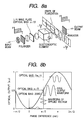
- Fig. 8a schematically shows a working principle of a typical optical fiber voltage (or electric field) sensor.
- a randomly polarized input beam transmitted from an optical fiber is passed to a polarizer wherein a linearly polarized beam component alone is transmitted.
- the beam transmitted through a ⁇ /4 plate is converted to a circularly polarized beam because the phase difference of the beam relative to the respective principal dielectric axes occurs by ⁇ /2.
- the beam undergoes a phase difference corresponding to a voltage applied to the element, and is changed in various forms including from circularly polarized beam to linearly polarized beam.
- Fig. 8a This is particularly shown in Fig. 8a as the state of polarized output beam. After transmission through an analyzer, the change in the polarized state is observed as a change in beam intensity.
- P and t of shaded sketches indicate a beam intensity and a time, and the sketches show that a beam with given powder is inputted, and a modulated beam is outputted at the positions depicted, respectively.
- Fig. 8b is a graph showing the relation between the beam output strength and the phase difference or optical bias of a fiber sensor.
- the quantity of transmission of output light or beam is determined by the phase difference of the beam based on an electrooptic effect and an optical bias (determined by a ⁇ /4 plate).
- the output beam intensity is expressed by SIN function.
- the optical bias is given by ⁇ /2 or by a multiple of an odd number of ⁇ /2, a portion of the SIN function, which exhibits good linearity, can be used.
- the optical bias is deviated from ⁇ /2, e.g. when the optical bias is at 3 ⁇ /4, the output waveform is distorted.
- the optical bias is considerably deviated (e.g.
- crystals which are free of spontaneous birefringence include, for example, BGO, BSO, Bi 4 Ge 3 O 12 and the like.
- BGO and BSO respectively, have the optical rotary power (i.e. the effect of the plane of polarization being rotated in proportion of the crystal length), so that the crystal length cannot be large, with the attendant problem that the degree of modulation of a beam cannot be optionally set and the degree of modulation cannot be sufficiently increased as described, for example, in the above-mentioned "Optical Fiber Sensors", edited by T. Ohkoshi, pp. 152 to 153.
- Bi 4 Ge 3 O 12 undesirably involves a DC drift at high temperatures, thus presenting the problem that when used as an optical modulator, a stable temperature characteristic is not ensured. This is particularly reported, for example, by O. Kamada (Jp. J. Appl. Phys. Vol. 32 (1993), pp. 4288 to 4291).
- any lens is not used. Accordingly, it is necessary to suppress an adverse influence caused by the divergence of a beam, disenabling one to take a sufficiently large crystal length. Accordingly, in case where LN, which has a relatively large electrooptic constant, is used as an electrooptic element, there arises the problem that sensitivity is not enough for use as an optical fiber sensor. Alternatively, if liquid crystals are used, problems are involved in that the response speed becomes very low, an abrupt change of voltage cannot be measured accurately, and such liquid crystals may be solidified when used at low temperatures.
- an optical fiber Where part of an optical fiber is poled and used as an electrooptic element, there arises a problem as experienced in the case of a sensor wherein an LN crystal is used as an electrooptic element and an incident beam is deviated from an optical axis (z axis). More particularly, if an optical fiber is poled at part thereof for use as an electrooptic element, not only a nonlinear optical effect (electrooptic effect), but also the anisotropy of refractive index (spontaneous birefringence) develops. When such a poled fiber is used in an optical fiber sensor, it is difficult to obtain an intended fiber sensor. This difficulty does not occur in known optical modulators wherein a change in refractive index based on the electrooptic effect of one of principal dielectric axes is utilized, and in fact, has not been recognized at all up to now.
- This optical fiber has such a function as a so-called "polarization-preserving fiber", and the polarized state of a beam inputted from portions other than principal dielectric axes (i.e. a line connecting a pair of holes and a direction normal to the line) becomes very unstable. If such an optical fiber is under varying temperature conditions or is applied with an external pressure thereon, the state of polarization of the beam changes considerably.
- this optical fiber is used as an electrooptic element and a beam, which has the direction of poling different from the principal dielectric axes, is inputted to the fiber, the degree of modulation greatly changes by changing a temperature, for example, only by several degrees in centigrade. Thus, the electrooptic element has a very poor temperature characteristic and a large distortion rate.
- an optical fiber modulator which comprises an optical fiber having a poled portion whereby the portion serves as an electrooptic element having an electrooptic effect and a function as a ⁇ /4 plate.
- an optical fiber modulator comprises an optical fiber, a substrate having a groove pattern in which the optical fiber is fixed, and a modulation unit including a polarizer, an electrooptic element, and an analyzer aligned in a light path of the optical fiber in this order, wherein the electrooptic element is made of a poled portion of the optical fiber, and when an electric field is not applied to the electrooptic element, i.e. when the electrooptic element is in an electric field-free condition, an absolute value, ⁇ , of a phase difference of a beam passed through the electrooptic element is within the following range (m/2 - 1/6) ⁇ ⁇ (m/2 + 1/6) ⁇ wherein m is an odd number.
- ⁇ is such that ⁇ /3 ⁇ ⁇ ⁇ 2 ⁇ /3.
- the poled portion is formed by properly poling from only one direction normal to the light path. It will be noted that the above-defined absolute value may be obtained when a portion of an optical fiber is successively poled from two different directions vertical to the light path under controlled poling conditions although the poling conditions are more complicated than those for the poling from one direction.
- an optical fiber modulator which comprises an optical fiber, a substrate having a groove pattern in which the optical fiber is fixed, and a modulation unit including a polarizer, an electrooptic element, and an analyzer aligned in a light path of the optical fiber in this order provided that a wave plate is provided between the polarizer and the electrooptic element or between the electrooptic element and the analyzer, wherein the electrooptic element is made of a poled portion of the optical fiber, and when the electrooptic element is in an electric field-free condition, an absolute value, ⁇ 1, of a phase difference of a beam passed through the wave plate and the electrooptic element is within the following range (n/2 - 1/6) ⁇ ⁇ 1 ⁇ (n/2 + 1/6) ⁇ wherein n is an odd number.
- ⁇ 1 is such that ⁇ /3 ⁇ ⁇ 1 ⁇ 2 ⁇ /3
- the poled portion serving as the electrooptic element in this embodiment is obtained by successively poling from two different directions.
- the two different directions should preferably be substantially normal to each other within a range of 90 degrees ⁇ 10 degrees.
- the optical fiber may be straight, or may be shaped in U form having a flat bottom. In the latter case, the modulation unit is arranged at the flat bottom.
- an optical fiber modulator which comprises an optical fiber, a substrate having a groove pattern in which the optical fiber is fixed, and a modulation unit including a polarizer, an electrooptic element, and an analyzer aligned in a light path of the optical fiber in this order, wherein the electrooptic element is made of a portion of the optical fiber, which is poled while observing a state of a polarized passed through the poled portion so that when the poled portion is in an electric field-free condition, an absolute value, ⁇ , of a phase difference of a beam passed through the poled portion is within the following range (m/2 - 1/6) ⁇ ⁇ (m/2 + 1/6) ⁇ wherein m is an odd number.
- the absolute value, ⁇ is preferably such that ⁇ /3 ⁇ ⁇ ⁇ 2/3 ⁇ wherein m is an odd number.
- the portion of the optical fiber may be poled in such a way that when the electrooptic element assembled in the modulator is applied with an AC electric field, a distortion rate of the modulation signals of a beam immediately after passage through the analyzer of the modulation unit is substantially in a minimum.
- the portion of the optical fiber is preferably poled from only one direction substantially vertical to the light path within a range of 90° ⁇ 10°.
- an optical fiber modulator which comprises an optical fiber, a substrate having a groove pattern in which the optical fiber is fixed, and a modulation unit including a polarizer, an electrooptic element, and an analyzer aligned in a light path of the optical fiber in this order provided that an wave plate is provided between the polarizer and the electrooptic element or between the electrooptic element and the analyzer, wherein the electrooptic element is made of a portion of the optical fiber, which is successively poled from two different directions substantially vertical to the light path within a range of 90 ⁇ 10 degrees while observing a state of polarization of a beam passed through both a wave plate having the same optical phase difference as the first-mentioned wave plate and the poled portion for each application of the electric field or voltage so that when the poled portion is in an electric field-free condition, an absolute value, ⁇ 1, of a phase difference of a beam passed through the poled portion is within the following range (n/2 -
- ⁇ 1 is such that ⁇ /3 ⁇ ⁇ 1 ⁇ 2 ⁇ /3.
- the poling may be effected such that when the electrooptic element assembled in the modulator is applied with an AC electric field, a distortion rate of the modulation signals of the beam immediately after passage through the analyzer in the modulation unit is substantially in a minimum.
- the optical fiber may be straight, or may be shaped in U form having a flat bottom.
- the modulator is effectively used as an optical fiber voltage or electric field sensor.
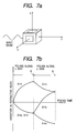
- glass or optical fibers develop not only a nonlinear optical effect (or electrooptic effect), but also anisotropy of refractive index.
- FIG. 7a there is shown an electrooptic element B in the form of a cubic block of a nonlinear optical material which is made, for example, of glass or an optical fiber capable of poling.
- the block is attached with electrodes along axes of x and y as shown.
- the x and y axes are shown to be intersected at right angles to each other, the intersection at right angles is not always necessary.
- the poling along the y axis is unlikely to be influenced by the results of an initial poling treatment along the x axis, ensuring easy control of the poling treatment along the y axis.
- the z axis is intersected substantially at right angles relative to the x and y axes, respectively.
- the direction of propagation of a beam i.e. an axial direction of the optical fiber, is determined as a z axis.
- the cubic block is heated, for example, to a temperature of 150 to 300°C, followed by application of an electric field ranging from 1 x 10 4 to 1 x 10 6 V/cm.
- an electric field ranging from 1 x 10 4 to 1 x 10 6 V/cm.
- the poled block is assembled in an optical system, as shown in Fig. 8a, without use of any ⁇ /4 plate, and the plane of polarization of an input beam (i.e. a linearly polarized beam) is set at an angle of 45° as viewed from the x axis toward the y axis, thereby observing a state of polarized beam.
- the electrooptic element consists of a circularly polarized beam as depicted at the center of the state of polarized beam in Fig. 8a, the poling treatment is completed.
- the term "circularly polarized beam” used herein means that a phase difference of the beam transmitted through the principal dielectric axes of the x and y axes is ⁇ /2 or a multiple of an odd number of ⁇ /2.
- the electrooptic element made in this manner is one which has an electrooptic effect and the function as an element serving as a wave plate capable of imparting an optical bias to the system. Accordingly, when using the electrooptic element, the resultant optical fiber modulator exhibits good linearity without use of any ⁇ /4 plate.
- the degree of the optical bias should preferably be ⁇ /2, which is an ideal value, or a multiple of an odd number thereof.
- the absolute value, 6, of the phase difference may be deviated from the ideal value within a range of about ⁇ /6. In this range, a degree of modulation is not deviated from a predetermined, designed value, and such a modulator is usable.
- a block of an optical fiber is poled for use as an electrooptic element in such a way that the phase difference of a beam transmitted through the poled portion in an electric field-free condition is expressed according to the following inequality wherein ⁇ is an absolute value of the phase difference
- an optical fiber modulator with good properties can be fabricated without use of any wave plate (m/2 - 1/6) ⁇ ⁇ ⁇ (m/2 + 1/6) ⁇ wherein m is an odd number.
- the degree of modulation suffers a great temperature change due to the great change of spontaneous birefringence depending on the temperature, so that a smaller value of m leads to a more stable optical fiber modulator. Accordingly, it is preferred to use the electrooptic element made of an optical fiber block poled in such a way that the absolute value, ⁇ , of the phase difference is given according to the following inequality ⁇ /3 ⁇ ⁇ ⁇ 2/3 ⁇
- the modulator using such an element as mentioned above exhibits a more stable temperature characteristic.
- the poling treatment can be completed such that when an AC voltage is applied to the electrooptic element, a distortion rate of the resultant beam output is substantially minimized.
- the minimization of the distortion rate can be simply confirmed through a spectrum analyzer. This observation enables one to make an electrooptic element which satisfies the above-defined inequalities with respect to the absolute value, ⁇ .
- the poling treatment is continued until the beam transmitted through the electrooptic element is polarized to provide a circularly polarized beam.
- the absolute value, ⁇ 1 of the total phase difference generated in the wave plate and the electrooptic element is a multiple of an odd number of ⁇ /2. It will be noted that the absolute value, ⁇ , of the phase difference generated by the electrooptic element alone is a multiple of an even number of ⁇ /2.
- the poling should be effected such that the absolute value, ⁇ 1, of the phase difference of a beam transmitted through a wave plate and the electrooptic element is expressed by the following inequality whereby a substantially optically isotropic electrooptic element can be obtained (n/2 - 1/6) ⁇ ⁇ 1 ⁇ (n/2 + 1/6) ⁇ wherein n is an odd number.
- the absolute value, ⁇ 1, of the phase difference transmitted through the wave plate and the electrooptic element is given by the following inequality ⁇ /3 ⁇ ⁇ 1 ⁇ 2/3 ⁇
- a ⁇ /4 plate is used as a wave plate.
- the wave plate consist of ⁇ /4 plate.
- the absolute value, ⁇ 1 of the phase difference transmitted through both the wave plate and the electrooptic element satisfies the above inequalities, the resultant modulator serves satisfactorily as an optical fiber modulator.
- the electrooptic element is in a condition where little spontaneous birefringence appears along the direction of beam transmission.
- the poling treatment is performed along both directions of the x and y axes, nz becomes small as is shown in Fig. 7b. If optically isotropic glass is poled, a change in refractive index is usually at a level of 0.001 or below.
- the quantity of birefringence of LN i.e.
- a difference between the maximal and minimal refractive indices is about 0.09, which is greater by two orders of magnitude than that of the nonlinear optical material, i.e. the poled block of an optical fiber.
- the accuracy in angle of a beam incident to the nonlinear optical material becomes greater by about two orders of magnitude than the accuracy of LN.
- the electrooptic element is isotropic with respect to the beam propagating along the z axis, the temperature change of birefringence becomes smaller than in the case where nx is not equal to ny. More particularly, in case where a refractive index changes depending on the change of temperature, the relation of nx ⁇ ny is maintained.
- the optical bias of the electrooptic element becomes so small that there can be made an optical fiber modulator including a voltage (electric field) sensor having a very good temperature characteristic.
- the optical fiber modulator can be used not only as the sensor, but also as a switching device or a modulation device for communication systems, which has a good temperature characteristic and a low distortion.
- an AC voltage may be applied to the electrooptic element so that the poling is completed at the time when the distortion rate of a beam output is in a minimum.
- an optical fiber modulator can be fabricated in which the phase difference of a beam transmitted through the wave plate and the electrooptic element is within a range of (n/2 - 1/6) ⁇ ⁇ 1 ⁇ (n/2 + 1/6) ⁇ , preferably ⁇ /3 ⁇ ⁇ 1 ⁇ 2/3 ⁇ , in terms of an absolute value thereof.
- the electrooptic element can be elongated, as desired, without use of any lens. Accordingly, an optical fiber modulator having a great degree of modulation can be realized.
- the beam input can be directed in the same way as the beam output, enabling one to make particularly a small-sized optical fiber sensor.
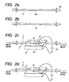
- FIG. 1 and 2a to 2c illustrate an optical fiber modulator according to one embodiment of the invention and a method for making such a modulator.
- an optical fiber 21 having a ferrule 201 at opposite ends thereof is provided as shown in Fig. 2a.
- the optical fiber used in the present invention may be any types of optical fibers capable of being poled.
- Such an optical fiber usually comprises silica.
- the optical fiber is made of a glass composition comprising silica, and Ge and/or lead, and is known as germanosilicate or lead silicate optical fibers.
- Ge and/or lead may be present in the optical fiber in an amount of from 5 to 20 wt%, based on the total composition, in the form of oxides or fluorides.
- Other additive oxides or fluorides of metals such as Te, Bi, Sn and the like may also be present in the glass composition in total amounts of up 40 wt% based on the composition.
- the optical fiber 21 may be either a single mode optical fiber or a multi mode optical fiber. When using a LED beam source, a multi mode optical fiber is preferred because a greater quantity of beam is taken in through the fiber.
- the optical fiber has such a structure which includes a core of the above-mentioned glass composition having a diameter, for example, of 200 ⁇ m and a cladding layer having a thickness, for example, of 250 ⁇ m, covered with a jacket 202.
- the core portion may be doped, for example, with GeO 2 so as to enhance its refractive index as is known in the art.
- the jacket 202 of the optical fiber 21 at a portion thereof is remove to provide a jacket-free, bare portion 22.
- the bare portion 22 consists of the core and the cladding layer but is free of any jacket and a buffering layer although a surface treating agent may be deposited on the cladding layer as used to permit intimate contact between the cladding layer and the buffer layer.
- the bare portion 22 is fixed in a groove of a heater 23 so that a portion to be poled is sandwiched between a pair of electrodes 20, 20'.
- the portion 22 is set so that it is poled along an x axis as shown, and the y axis indicated in the figure is a direction determined to be substantially normal to the x axis within a range of 90 ⁇ 10 degrees and the z axis is determined as a direction along which a beam propagates.
- the z axis is substantially normal to the x or y axis within a range of 90 ⁇ 10 degrees.
- the optical fiber is maintained straight, through which substantially collimate light is passed as an input beam to confirm that the state of a polarized beam during the course of propagation through the optical fiber is in order.
- the portion 24 to be poled is heated to a temperature ranging from 150 to 350 °C by means of the heater 23, followed by application of a voltage, for example, of 5 kV from an electric supply 25. when a space between the electrodes is 5 mm, for a time of 30 to 100 minutes. In this way, the poling treatment along the x axis is performed.
- the portion 24 to be poled has a length corresponding to an electrode length, and can be arbitrarily changed in length by changing the electrode length. In general, the length of a poled portion is within a range of 0.3 to 5 cm depending on the purpose.
- the poling along the x axis is described above. The direction may be along the y axis, which is also substantially vertical to the light path or the z axis.
- optical fiber having the poled portion as described above is used to make a linear optical fiber modulator shown in Fig. 1.
- an optical fiber modulator M including a substrate 10 having a straight groove 11 and an optical fiber 12 having a bare fiber portion 13 and a poled portion 14 attached with an electrode 15 at opposite sides of the portion 14.
- the poled portion 14 serves as an electrooptic element.
- the substrate 10 has two further grooves 17a, 17b made normal to the first-mentioned straight groove 11.
- a polarizer 18 is set in the groove 17a, and an analyzer 19 is set in the groove 17b so that the polarizer 18, the electrooptic element 14 and the analyzer 19 are aligned in a light path of the optical fiber 12.
- a power supply V has leads 20a, 20b, and the lead 20a is electrically connected to the upper electrode 15.
- the lead 20b is electrically connected to the other electrode 15 (not shown) attached to a corresponding portion of the substrate 10 which has been made thin to about 0.1 mm
- the substrate 10 may be made of insulating materials such as glass, ceramics, resins and the like. In view of good processability and insulating properties, a glass-epoxy resin substrate is preferred.
- the substrate 10 is first provided, and the groove 11 is formed in the substrate 10 by means of a rotary blade saw.
- the optical fiber 12 is fixed to the groove 11 by means of a ceramic or epoxy resin bonding agent.
- the grooves 17a, 17b are made in the substrate 10 at opposite ends of the poled portion 14 by means of a rotary blade saw so that the bare portion 13 of the optical fiber 12 is also cut away.
- the optical elements 18, 19 are set in the light path of the optical fiber 12.
- the polarizer 18 and the analyzer 19 are, respectively, bonded to and fixed in the grooves 17a, 17b by a usual manner.
- the electrodes 15 are disposed on opposite sides of the poled portion 14 provided that one of the electrodes 15 is bonded to a portion at a lower side of the substrate 10 which has been made thin beforehand.
- a beam from LED is passed as an input beam from one end of the optical fiber 12 as shown, and an AC voltage of 1000 V is applied to the electrooptic element 14 via the leads 20a, 20b connected to the respective electrodes 15 to determine a degree of modulation of an output beam, revealing that a degree of modulation is 1.8% with a distortion rate of 1%.
- the distortion rate is degraded when the absolute value, ⁇ , of the phase difference of the beam transmitted through the electrooptic element deviates from m x ⁇ /2, but within a range of ⁇ /6 relative to a preset value, the lowering of a modulation signal is not appreciable.
- the electrooptic element is usable in the optical fiber modulator.
- the modulator having a degree of modulation of 1.8% is further subjected to measurement of a temperature characteristic within a range of -20 to +80°C, the variation is within ⁇ 5% relative to a degree of modulation at room temperature taken at 100%.
- the poled portion in this instance serves both wave plate and electrooptic element, any wave plate is unnecessary.
- the modulator M is placed at high temperatures of 70°C or above, no DC drift is observed, unlike an optical modulator comprising a crystal plate of Bi 4 Ge 3 O 12 , thereby ensuring a stable temperature characteristic.
- the poling treatment is performed by heating an optical fiber and applying a high voltage to the heated fiber.
- the poling may likewise proceed when a high electric field is applied to an optical fiber while exposing to UV light.
- there may be used other methods including a corona poling method, or a method of poling under high vacuum and high temperature conditions.
- an optical fiber is maintained straight, and it is confirmed that the state of polarization of a beam being propagating through the fiber is in order.
- the direction of initial poling is taken as x axis, and a direction substantially normal to the x axis within a range of 90 degrees ⁇ 10 degrees is taken as y axis.
- the direction of a beam being propagated is taken as z axis shown in Fig. 2c.
- the portion 24 to be poled of the optical fiber 21 is heated to 300° by means of the heater 23 and poled by applying a voltage of 5 kV (at an electrode space of 0.5 mm) for 100 minutes to pole the portion 24 along the x axis as shown in Fig. 2c.
- the optical fiber is turned about the z axis within a range of 90 degrees ⁇ 10 degrees, followed by poling at 300°C for 30 minutes by application of a voltage of 5 kV as shown in Fig. 2d.
- the thus poled fiber is returned to room temperature, at which a linearly polarized beam is inputted from the left-hand end face of the optical fiber as viewed in Fig. 2d to observe a state of polarization of an output beam.
- the beam is inputted such that the plane of polarization of the linearly polarized input beam is set at an angle of 45° as viewed from the x axis toward the y axis.
- the poling is further continued. After returning the further poled fiber to room temperature, the state of a polarized beam is observed in the same manner as described above, and the poling is completed when the transmitted beam consists of a linearly polarized beam.
- FIG. 3 The thus poled optical fiber is assembled in an optical modulator M shown in Fig. 3 in the same manner as illustrated with reference to Fig. 1.
- like reference numerals as in Fig. 1 indicate like parts or members, respectively, provided that reference numeral 18' in Fig. 3 indicates polarizer + ⁇ /4 plate, and reference numeral 14' indicates an electrooptic element made of the portion of an optical fiber poled from two different directions and illustrated above.
- the absolute value, ⁇ 1 of the phase difference of a beam transmitted through a wave plate having the same optical phase difference as the wave plate used in the wave plate + polarizer 18 and the electrooptic element is a multiple of an odd number of ⁇ /2, good linearity is obtained. Further, when a deviation from the multiple of an odd number of ⁇ /2 is within ⁇ /6, modulated signals can be obtained, and such a modulator is usable as an optical fiber modulator or sensor.
- the temperature characteristic is best when the absolute value, ⁇ 1, is ⁇ /2.
- the wave plate + electrooptic element 18 may be reversed in order provided that the principal dielectric axis of the wave plate and that of the electrooptic element are coincident with each other.
- the wave plate may be attached to the analyzer. This is true of other embodiments which comprises both wave plate and electrooptic element.
- An optical fiber modulator M shown in Fig. 4e includes a substrate 40, which has a groove pattern 41 constituted of three grooves 41a, 41b, 41c, and grooves 42, 43 formed substantially normal to the groove 41c, and a U-shaped optical fiber 44 having a bare portion 44a and flat bottom 44b.
- the electrooptic element 46 is made of a portion of the optical fiber 44, which is poled in one direction vertical to a light path where a beam propagates in the optical fiber 44.
- the electrodes 47 and 47' are connected to leads 50 and 50', respectively, which are connected to a power supply (not shown).
- the optical fiber modulator M having individual elements integrated in a hybrid manner is arranged as shown in Fig. 4e.
- the substrate 40 is first provided as shown in Fig. 4a.
- the substrate 40 is made of a heat-resistant material such as BK7 glass in view of the fact that the substrate 40 is heated when the optical fiber 44 is poled at part thereof.
- grooves 41a, 41b and 41c are made by use of a rotary blade saw to form a groove pattern 41 as shown in Fig. 4b.
- grooves 49, 49' are formed in which the electrodes 47, 47' are inserted to sandwich a portion 46a to be poled.
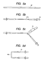
- the optical fiber 44 which has a U form having the flat bottom 44b, is made in a manner described hereinafter.
- the optical fiber 44 has the bare portion 44a from which a jacket is removed.
- the optical fiber 44 is set in the groove pattern 41 and bonded to the substrate 40 as shown in Fig. 4c.
- the bonding agents used for this purpose may be ceramic bonding agents comprising alumina and/or silica powder.
- a straight optical fiber 44' is first provided as shown in Fig. 5a, and a jacket is removed from part of the fiber 44' to provide a bare fiber 44'a as shown in Fig. 5b.
- the optical fiber 44' is provided with a ferrule 52 at opposite ends thereof.
- the bare optical fiber 44a has, for example, a silica core with a diameter of 200 ⁇ m and a cladding layer covering the core therewith and having a diameter of 250 ⁇ m.
- the core is doped with GeO 2 in order to enhance a refractive index. This type of fiber has a softening temperature of 900 to 1000°C.
- the bare fiber 44a can be shaped, as desired, by use of a micro gas burner 54 in a manner as shown in Fig. 5c to provide a U-shaped fiber 44 having a flat bottom 44b as shown in Fig. 5d.
- This U-shaped fiber 44 is used in Fig. 4c.
- Figs. 4d and 4e grooves 42, 43 are made by means of a rotary blade saw, at which part of the optical fiber 44 in the groove pattern 41 is removed.
- the polarizer 45 and the analyzer 48 are set in the grooves 42, 43, respectively, and bonded to the substrate 40.
- Electrodes 47, 47' made of a stainless steel thin sheet are, respectively, inserted into the grooves 49, 49' as shown in Fig. 5e.
- the space between the electrodes 47, 47' is, for example, 1 mm.
- Lead wires 50, 50' are electrically connected to the electrodes 47, 47', respectively, at one end thereof, and are connected to a power supply for poling treatment or for measurement of a degree of modulation at the other end of each wire.
- an optical fiber from a light source (not shown) is connected to at one end of the optical fiber 44 and another optical fiber from a light-receiving device (not shown) is connected to the other end of the optical fiber 44, a system of measuring a modulation signal of the optical fiber modulator M can be arranged.
- a heater (not shown) is intimately contacted with at an upper portion of the substrate 40 as viewed in Fig. 4e.
- the substrate is heated to 200°C in an atmosphere of dry nitrogen, and the portion 46 of the optical fiber 44 attached with the electrodes 47, 47' is poled by application of a potential of 10 kV for 30 minutes, for example.
- the lead wires 50, 50' are connected to a power supply (not shown) for poling.
- the poling is stopped, and the connection of the lead wires 50, 50' is changed to a power supply for the measurement of a degree of modulation.
- An AC voltage of 1000 V is applied across the electrodes to measure a distortion rate of a modulation signal. If the distortion rate is larger than intended, the poling is further continued in a manner as described above until the distortion rate is 1% or below when an AC voltage of 1000 V is applied to.
- the resultant modulator is cooled down to room temperature to complete the poling treatment.
- the optical fiber modulator obtained in this manner has a degree of modulation of 1.0% and a distortion rate of 0.8% relative to an AC waveform of SIN wave.
- the portion of the optical fiber is poled only in one direction and serves as both electrooptic element and wave plate. Accordingly, modulation signals with good linearity can be obtained without use of any wave plate.
- This type of optical fiber modulator has the directions of beam input and output, which are parallel to each other.
- the size of the modulator can be made smaller than those modulators of Figs. 1 and 3, and thus, the modulator is especially suitable as a sensor.
- FIG. 5c to 5d A still further embodiment is illustrated with reference to Figs. 5c to 5d and Figs. 6a to 6d.
- like reference numerals as in Figs. 4a to 4d indicate like parts or members, respectively.
- An optical fiber modulator M of this embodiment is similar to the modulator illustrated with reference of Figs. 4a to 4d except that a portion of an optical fiber is poled from two different directions along the x and y axes as illustrated in Figs. 2c and 2d or in Fig. 7a and that a wave plate is used.
- the portion of the optical fiber is so poled in this embodiment that the phase difference of a beam transmitted through a ⁇ /4 plate and the electrooptic element is just ⁇ /2, for example.
- the optical fiber is poled at a portion thereof in a manner as illustrated in Figs. 2a to 2d.
- the thus poled fiber is shaped according to the procedure shown in Figs. 5c and 5d. More particularly, the optical fiber heated by means of the micro gas burner 54 to form a U-shaped optical fiber having a flat bottom 44b. In order not to apply heat to the poled portion, two corners of the U shape are processed within a short time, for example, of 10 to 30 seconds while closing down a burner tip to use a fine flame.
- a substrate 40 In this case, the substrate is not heated and may be made of a glass-epoxy resin.
- a groove pattern 41 is made as in the foregoing embodiment.
- the U-shaped optical fiber 44 is set in the groove pattern 41 and bonded to the substrate 40 as shown in Fig. 6b.
- Grooves 42, 43 are formed for inserting optical elements therein. That is, a polarizer element 45a made of a polarizer and a ⁇ /4 plate made of quartz and integrally combined with the polarizer is fixed in the groove 42, and an analyzer 48 is fixed in the groove 43 as shown in Fig. 6d.
- a poled portion 46a of the optical fiber 41 is bonded with an electrode 60 on an upper side thereof.
- Another electrode (not shown) is bonded to a rear side of the substrate 40 at a portion processed to a thickness of about 0.2 mm, thereby obtain an optical fiber modulator shown in Fig. 6d.
- lead wires connected to the electrodes are not shown for convenience sake.
- any measure of suppressing an optical loss at the bent portions of the shaped optical fibers with reference to Figs. 4a to 4e and Figs. 6a to 6d is not made. If it is desirable to minimize an optical loss, a beam reflection dielectric multi-layered film or metallic paste coating may be formed on the bent portions.
Abstract
Description
Preferably, δ is such that π/3 ≤ δ ≤ 2π/3.
Claims (18)
- An optical fiber modulator which comprises an optical fiber, a substrate having a groove pattern in which the optical fiber is fixed, and a modulation unit including a polarizer, electrooptic element, and an analyzer aligned in a light path of the optical fiber in this order, wherein the electrooptic element is made of a poled portion of the optical fiber, and when the electrooptic element is in an electric field-free condition, an absolute value, δ, of a phase difference of a beam passed through said electrooptic element is within the following range
- An optical fiber modulator according to Claim 1, wherein absolute value, δ, is such that π/3 ≤ δ ≤ 2π/3.
- An optical fiber modulator according to Claim 1 or 2, wherein the poled portion is obtained by poling from one direction normal to the light path.
- An optical fiber modulator which comprises an optical fiber, a substrate having a groove pattern in which the optical fiber is fixed, and a modulation unit including a polarizer, an electrooptic element, and an analyzer aligned in a light path of the optical fiber in this order provided that a wave plate is provided between the polarizer and the electrooptic element and the analyzer, wherein said electrooptic element is made of a poled portion of the optical fiber, and when the electrooptic element is in an electric field-free condition, an absolute value, δ1, of a phase difference of a beam passed through said wave plate and said electrooptic element is within the following range
- An optical modulator according to Claim 4, wherein the absolute value, δ1, is such that π/3 ≤ δ1 ≤ 2π/3
- An optical modulator according to Claim 4 or 5, wherein the poled portion is one poled from two different directions.
- An optical modulator according to Claim 6, wherein the two different directions are substantially vertical to each othre within a range of 90° ± 10°.
- An optical fiber modulator according to any one of claims 1 to 7 wherein said optical fiber is straight.
- An optical fiber modulator according to any one of claims 1 to 7 wherein said optical fiber has a U form having a flat bottom in which said modulation unit is set.
- A method for making an optical fiber modulator which comprises an optical fiber, a substrate having a groove pattern in which said optical fiber, and a modulation unit including a polarizer, electrooptic element, and an analyzer aligned in a light path of the optical fiber in this order, wherein said elecrooptic element is made of a portion of said optical fiber, which is poled while observing a state of a polarized beam passed through the poled portion so that when the poled portion is in an electric-field-free condition, an absolute value, δ, of a phase difference of abeam passed through the poled portion is within the following range
- A method according to Claim 10, wherein absolute value, 6, is such that π/3 ≤ δ ≤ 2/3π.
- A method according to Claim 10 or 11, wherein the poling is effected such that when an AC electric field is applied to said electrooptic element assembled in said modulator, a distortion rate of a modulation signal of the beamimmediately after transmission through said electrooptic element is in a minimum.
- A method according to Claim 10, 11 or 12, wherein said portion is poled from one direction substantially normal to the light path a range of 90±10 degrees.
- A method for making an optical fiber modulator which comprises an optical fiber, a substrate having a groove pattern in which the optical fiber is fixed, and a modulation unit including a polarizer, an electrooptic element, and an analyzer aligned in a light path of the optical fiber in this order provided that a wave plate is provided between the polarizer and the electrooptic element or between the electrooptic element and the analyzer, wherein said electrooptic element is made of a portion of the optical fiber, which is subjected to poling by successively applying an electric field or voltage from two different directions substantially vertical to the light path within a range of 90±10 degress while observing a state of polarization of a beam passed through a wave plate having the same optical phase difference as the first-mentioned wave plate and the poled portion for each application of the electric field or voltage so that when the poled portion is in an electric field-free condition, an absolute value, δ1, of a phase difference of a beam passed through the poled portion is within the following range
- A method according to Claim 14, wherein the absolute value, δ1, is such that π/3 ≤ δ1 ≤ 2π/3.
- A method according to Claim 14 or 15, wherein the poling is effected such that when an AC electric field is applied to electrooptic element, a distortion tate of a modulation signal of the beam immediately after transmission through the analyzer minimized.
- A method according to any one of claims 10 to 16, wherein said optical fiber is straight.
- A method according to any one of claims 10 to 16, wherein said optical fiber is shaped in U form having a flat bottom, at which said modulation unit is set.
Applications Claiming Priority (6)
| Application Number | Priority Date | Filing Date | Title |
|---|---|---|---|
| JP7540797 | 1997-03-27 | ||
| JP7540797 | 1997-03-27 | ||
| JP75407/97 | 1997-03-27 | ||
| JP72615/98 | 1998-03-20 | ||
| JP7261598 | 1998-03-20 | ||
| JP07261598A JP4097764B2 (en) | 1997-03-27 | 1998-03-20 | Light modulation element and manufacturing method thereof |
Publications (3)
| Publication Number | Publication Date |
|---|---|
| EP0867743A2 true EP0867743A2 (en) | 1998-09-30 |
| EP0867743A3 EP0867743A3 (en) | 1999-09-15 |
| EP0867743B1 EP0867743B1 (en) | 2003-05-14 |
Family
ID=26413742
Family Applications (1)
| Application Number | Title | Priority Date | Filing Date |
|---|---|---|---|
| EP98302357A Expired - Lifetime EP0867743B1 (en) | 1997-03-27 | 1998-03-27 | Optical fiber modulator having an optical fiber having poled portion serving as an electrooptic element and method for making same |
Country Status (5)
| Country | Link |
|---|---|
| US (1) | US6008927A (en) |
| EP (1) | EP0867743B1 (en) |
| JP (1) | JP4097764B2 (en) |
| KR (1) | KR100297951B1 (en) |
| DE (1) | DE69814509T2 (en) |
Cited By (3)
| Publication number | Priority date | Publication date | Assignee | Title |
|---|---|---|---|---|
| US6259830B1 (en) | 1999-11-30 | 2001-07-10 | Corning, Incorporated | Poled electro-optic device and method |
| EP1125159A1 (en) * | 1998-10-31 | 2001-08-22 | The Board Of Trustees Of The Leland Stanford Junior University | Electrostrictive fiber modulators |
| WO2003023320A1 (en) * | 2001-09-10 | 2003-03-20 | The University Of Sydney | Suppressed drift interferometer |
Families Citing this family (11)
| Publication number | Priority date | Publication date | Assignee | Title |
|---|---|---|---|---|
| AU753632B2 (en) * | 1998-08-25 | 2002-10-24 | Alcoa Fujikura Limited | Single-sided fiber optic splitter with integral miniature bend |
| US6870595B1 (en) * | 1998-09-22 | 2005-03-22 | Minolta Co., Ltd. | Optical filter device and method of making same |
| KR100332833B1 (en) * | 1999-04-23 | 2002-04-17 | 윤덕용 | Transmission-type extrinsic Fabry-Perot interferometric optical fiber sensor |
| JP2001041983A (en) * | 1999-07-29 | 2001-02-16 | Matsushita Electric Ind Co Ltd | Photo-voltage sensor |
| US6766082B2 (en) * | 2000-10-18 | 2004-07-20 | Nippon Telegraph And Telephone Corporation | Waveguide-type optical device and manufacturing method therefor |
| KR100403673B1 (en) * | 2001-12-12 | 2003-10-30 | 한국전자통신연구원 | Method for forming on a fiber two thin conductive films isolated electrically each other |
| DE102006002605B4 (en) | 2006-01-13 | 2018-09-13 | Hans Joachim Eichler | Optical module with an optical fiber and a Fabry-Perot layer structure as electro-optical modulator and tunable filter |
| JP2012252210A (en) * | 2011-06-03 | 2012-12-20 | Toyota Industries Corp | Optical modulator |
| CN109001517B (en) * | 2018-05-02 | 2021-04-09 | 上海大学 | All-fiber voltage sensing device based on manganese-doped quartz fiber |
| RU2680990C1 (en) * | 2018-05-22 | 2019-03-01 | Общество с ограниченной ответственностью "Т8" (ООО "Т8") | Coplanar waveguide of electrooptic modulator of traveling of wave on basis of mach-zehnder interferometer |
| KR102288214B1 (en) | 2020-10-16 | 2021-08-11 | 주식회사 스토리코리아 | Wooden chopping board |
Citations (2)
| Publication number | Priority date | Publication date | Assignee | Title |
|---|---|---|---|---|
| EP0717294A2 (en) * | 1994-12-12 | 1996-06-19 | Matsushita Electronic Components Co., Ltd. | Optical fiber sensors and method for making the same |
| JPH09230293A (en) * | 1996-02-21 | 1997-09-05 | Furukawa Electric Co Ltd:The | Optical fiber type modulation device |
Family Cites Families (3)
| Publication number | Priority date | Publication date | Assignee | Title |
|---|---|---|---|---|
| JP2521537B2 (en) * | 1989-07-12 | 1996-08-07 | 松下電器産業株式会社 | Assembling method of voltage sensor |
| JPH05297086A (en) * | 1991-07-03 | 1993-11-12 | Matsushita Electric Ind Co Ltd | Optical magnetic field sensor |
| JPH0674979A (en) * | 1992-08-25 | 1994-03-18 | Nissin Electric Co Ltd | Optical current sensor |
-
1998
- 1998-03-20 JP JP07261598A patent/JP4097764B2/en not_active Expired - Fee Related
- 1998-03-27 KR KR1019980010737A patent/KR100297951B1/en not_active IP Right Cessation
- 1998-03-27 DE DE69814509T patent/DE69814509T2/en not_active Expired - Lifetime
- 1998-03-27 EP EP98302357A patent/EP0867743B1/en not_active Expired - Lifetime
- 1998-03-27 US US09/049,099 patent/US6008927A/en not_active Expired - Lifetime
Patent Citations (2)
| Publication number | Priority date | Publication date | Assignee | Title |
|---|---|---|---|---|
| EP0717294A2 (en) * | 1994-12-12 | 1996-06-19 | Matsushita Electronic Components Co., Ltd. | Optical fiber sensors and method for making the same |
| JPH09230293A (en) * | 1996-02-21 | 1997-09-05 | Furukawa Electric Co Ltd:The | Optical fiber type modulation device |
Non-Patent Citations (2)
| Title |
|---|
| FUJIWARA T ET AL: "Large electrooptic modulation in a thermally-poled germanosilicate fiber" IEEE PHOTONICS TECHNOLOGY LETTERS, OCT. 1995, USA, vol. 7, no. 10, pages 1177-1179, XP000537229 ISSN: 1041-1135 * |
| PATENT ABSTRACTS OF JAPAN vol. 098, no. 001, 30 January 1998 (1998-01-30) & JP 09 230293 A (FURUKAWA ELECTRIC CO LTD:THE), 5 September 1997 (1997-09-05) * |
Cited By (4)
| Publication number | Priority date | Publication date | Assignee | Title |
|---|---|---|---|---|
| EP1125159A1 (en) * | 1998-10-31 | 2001-08-22 | The Board Of Trustees Of The Leland Stanford Junior University | Electrostrictive fiber modulators |
| EP1125159A4 (en) * | 1998-10-31 | 2002-10-16 | Univ Leland Stanford Junior | Electrostrictive fiber modulators |
| US6259830B1 (en) | 1999-11-30 | 2001-07-10 | Corning, Incorporated | Poled electro-optic device and method |
| WO2003023320A1 (en) * | 2001-09-10 | 2003-03-20 | The University Of Sydney | Suppressed drift interferometer |
Also Published As
| Publication number | Publication date |
|---|---|
| KR19980080784A (en) | 1998-11-25 |
| KR100297951B1 (en) | 2001-09-06 |
| JP4097764B2 (en) | 2008-06-11 |
| US6008927A (en) | 1999-12-28 |
| DE69814509D1 (en) | 2003-06-18 |
| DE69814509T2 (en) | 2004-03-25 |
| EP0867743B1 (en) | 2003-05-14 |
| EP0867743A3 (en) | 1999-09-15 |
| JPH10325944A (en) | 1998-12-08 |
Similar Documents
| Publication | Publication Date | Title |
|---|---|---|
| EP0867743B1 (en) | Optical fiber modulator having an optical fiber having poled portion serving as an electrooptic element and method for making same | |
| JP3258520B2 (en) | Optical fiber sensor and method of manufacturing the same | |
| Jaeger et al. | Integrated optics Pockels cell high-voltage sensor | |
| US6766082B2 (en) | Waveguide-type optical device and manufacturing method therefor | |
| JP5278986B2 (en) | Light modulator | |
| EP0881528B1 (en) | Method for making a second-order nonlinear optical material, the material obtained by the method, and an optical modulation device comprising the material | |
| WO1998047041A1 (en) | Optical modulator | |
| Lee et al. | Integrated optical high-voltage sensor using a Z-cut LiNbO/sub 3/cutoff modulator | |
| US5923795A (en) | Optical waveguide device having a double-refractor at an input thereof | |
| JP3573180B2 (en) | Polling method for Mach-Zehnder interferometer arm | |
| CN105074545B (en) | The manufacturing method of optical waveguide components and optical waveguide components | |
| JP2613942B2 (en) | Waveguide type optical device | |
| JP2739405B2 (en) | Electric field sensor | |
| Nagata et al. | Refractive index fluctuations in deformed Ti: LiNbO3 waveguides due to SiO2 overlayer deposition | |
| JPH0588123A (en) | Variable wavelength filter | |
| JP3235301B2 (en) | Light voltage sensor | |
| US6920254B1 (en) | Method for controlling the polarization of an optical signal and an optical component for polarization control of light in planar waveguides | |
| JP3036610B2 (en) | Polarization direction switch | |
| Jung et al. | Interferometric polarization-independent modulator in LiTaO/sub 3 | |
| JPS6283731A (en) | Optical switch | |
| JP2003215517A (en) | Variable light attenuator and optical module using the same | |
| Findakly | Proton-exchanged integrated optical components | |
| JP2004264872A (en) | Optical device using photonic crystal | |
| JPS61145508A (en) | Optical coupler | |
| JPH06201935A (en) | Waveguide type optical control device and its manufacture |
Legal Events
| Date | Code | Title | Description |
|---|---|---|---|
| PUAI | Public reference made under article 153(3) epc to a published international application that has entered the european phase |
Free format text: ORIGINAL CODE: 0009012 |
|
| 17P | Request for examination filed |
Effective date: 19980406 |
|
| AK | Designated contracting states |
Kind code of ref document: A2 Designated state(s): DE FR GB |
|
| AX | Request for extension of the european patent |
Free format text: AL;LT;LV;MK;RO;SI |
|
| PUAL | Search report despatched |
Free format text: ORIGINAL CODE: 0009013 |
|
| AK | Designated contracting states |
Kind code of ref document: A3 Designated state(s): AT BE CH DE DK ES FI FR GB GR IE IT LI LU MC NL PT SE |
|
| AX | Request for extension of the european patent |
Free format text: AL;LT;LV;MK;RO;SI |
|
| RIC1 | Information provided on ipc code assigned before grant |
Free format text: 6G 02F 1/01 A, 6G 01R 15/24 B |
|
| AKX | Designation fees paid |
Free format text: DE FR GB |
|
| GRAH | Despatch of communication of intention to grant a patent |
Free format text: ORIGINAL CODE: EPIDOS IGRA |
|
| GRAH | Despatch of communication of intention to grant a patent |
Free format text: ORIGINAL CODE: EPIDOS IGRA |
|
| GRAA | (expected) grant |
Free format text: ORIGINAL CODE: 0009210 |
|
| AK | Designated contracting states |
Designated state(s): DE FR GB |
|
| REG | Reference to a national code |
Ref country code: GB Ref legal event code: FG4D |
|
| REF | Corresponds to: |
Ref document number: 69814509 Country of ref document: DE Date of ref document: 20030618 Kind code of ref document: P |
|
| ET | Fr: translation filed | ||
| PLBE | No opposition filed within time limit |
Free format text: ORIGINAL CODE: 0009261 |
|
| STAA | Information on the status of an ep patent application or granted ep patent |
Free format text: STATUS: NO OPPOSITION FILED WITHIN TIME LIMIT |
|
| 26N | No opposition filed |
Effective date: 20040217 |
|
| PGFP | Annual fee paid to national office [announced via postgrant information from national office to epo] |
Ref country code: FR Payment date: 20120319 Year of fee payment: 15 |
|
| PGFP | Annual fee paid to national office [announced via postgrant information from national office to epo] |
Ref country code: GB Payment date: 20120321 Year of fee payment: 15 |
|
| PGFP | Annual fee paid to national office [announced via postgrant information from national office to epo] |
Ref country code: DE Payment date: 20120411 Year of fee payment: 15 |
|
| GBPC | Gb: european patent ceased through non-payment of renewal fee |
Effective date: 20130327 |
|
| REG | Reference to a national code |
Ref country code: FR Ref legal event code: ST Effective date: 20131129 |
|
| REG | Reference to a national code |
Ref country code: DE Ref legal event code: R119 Ref document number: 69814509 Country of ref document: DE Effective date: 20131001 |
|
| PG25 | Lapsed in a contracting state [announced via postgrant information from national office to epo] |
Ref country code: DE Free format text: LAPSE BECAUSE OF NON-PAYMENT OF DUE FEES Effective date: 20131001 Ref country code: FR Free format text: LAPSE BECAUSE OF NON-PAYMENT OF DUE FEES Effective date: 20130402 Ref country code: GB Free format text: LAPSE BECAUSE OF NON-PAYMENT OF DUE FEES Effective date: 20130327 |