EP0890845A2 - S/N measuring circuit and method - Google Patents
S/N measuring circuit and method Download PDFInfo
- Publication number
- EP0890845A2 EP0890845A2 EP19980112863 EP98112863A EP0890845A2 EP 0890845 A2 EP0890845 A2 EP 0890845A2 EP 19980112863 EP19980112863 EP 19980112863 EP 98112863 A EP98112863 A EP 98112863A EP 0890845 A2 EP0890845 A2 EP 0890845A2
- Authority
- EP
- European Patent Office
- Prior art keywords
- circuit
- output
- electric power
- signal
- value
- Prior art date
- Legal status (The legal status is an assumption and is not a legal conclusion. Google has not performed a legal analysis and makes no representation as to the accuracy of the status listed.)
- Granted
Links
Images


Classifications
-
- H—ELECTRICITY
- H04—ELECTRIC COMMUNICATION TECHNIQUE
- H04W—WIRELESS COMMUNICATION NETWORKS
- H04W52/00—Power management, e.g. TPC [Transmission Power Control], power saving or power classes
- H04W52/04—TPC
- H04W52/18—TPC being performed according to specific parameters
- H04W52/24—TPC being performed according to specific parameters using SIR [Signal to Interference Ratio] or other wireless path parameters
-
- G—PHYSICS
- G01—MEASURING; TESTING
- G01R—MEASURING ELECTRIC VARIABLES; MEASURING MAGNETIC VARIABLES
- G01R29/00—Arrangements for measuring or indicating electric quantities not covered by groups G01R19/00 - G01R27/00
- G01R29/26—Measuring noise figure; Measuring signal-to-noise ratio
-
- H—ELECTRICITY
- H04—ELECTRIC COMMUNICATION TECHNIQUE
- H04W—WIRELESS COMMUNICATION NETWORKS
- H04W52/00—Power management, e.g. TPC [Transmission Power Control], power saving or power classes
- H04W52/04—TPC
- H04W52/06—TPC algorithms
- H04W52/08—Closed loop power control
-
- Y—GENERAL TAGGING OF NEW TECHNOLOGICAL DEVELOPMENTS; GENERAL TAGGING OF CROSS-SECTIONAL TECHNOLOGIES SPANNING OVER SEVERAL SECTIONS OF THE IPC; TECHNICAL SUBJECTS COVERED BY FORMER USPC CROSS-REFERENCE ART COLLECTIONS [XRACs] AND DIGESTS
- Y02—TECHNOLOGIES OR APPLICATIONS FOR MITIGATION OR ADAPTATION AGAINST CLIMATE CHANGE
- Y02D—CLIMATE CHANGE MITIGATION TECHNOLOGIES IN INFORMATION AND COMMUNICATION TECHNOLOGIES [ICT], I.E. INFORMATION AND COMMUNICATION TECHNOLOGIES AIMING AT THE REDUCTION OF THEIR OWN ENERGY USE
- Y02D30/00—Reducing energy consumption in communication networks
- Y02D30/70—Reducing energy consumption in communication networks in wireless communication networks
Definitions
- the present invention relates to a transmitting electric power control apparatus used in a digital mobile communicating system.
- transmitting electric power control is used for suppressing consumption of electric power at a mobile station while maintaining reception quality at a desired value, and for avoiding unnecessary interference with other mobile stations.
- the transmitting electric power control is essential.
- a Signal-to-Noise Power Ratio (referred to as an S/N, hereinafter) is measured from a signal received and demodulated at a base station, instruction is sent to the mobile station so that this S/N value will be a value enough for desired reception quality, and transmitting electric power is sequentially controlled.
- a noise N used here includes a thermal noise and an interference signal.
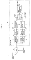
- Fig. 4 is a view showing an S/N measuring circuit of the first prior art.
- an S/N measuring circuit 50 of the first prior art is constructed of a modulation removing circuit 3 connected to an analog-digital (A/D) converter 2, a first averaging circuit 4, a first square operating circuit 5, a second square operating circuit 6 connected to the analog-digital (A/D) converter 2, a second averaging circuit 7, a subtracting circuit 8, and a dividing circuit 9.
- a demodulated reception signal is sampled at a modulation clock by the A/D converter 2.
- the S/N measuring circuit after a modulated component of an output of the A/D converter 2 is removed in the modulation removing circuit 3, the output is averaged over a plurality of symbol sections in the first averaging circuit 4, and an amplitude value in which a noise component is suppressed is obtained.
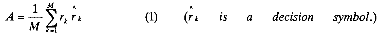
- An output of the first averaging circuit 4 is squared by the first square operating circuit 5, and desired signal power S is obtained.
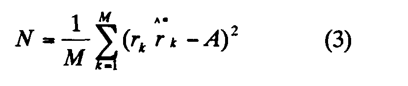
- an output of the A/D converter 2 is supplied to the second square operating circuit 6, and is converted into time series having a dimension of electric power. Thereafter, the output is averaged over a plurality of symbol sections by the second averaging circuit 7, and total electric power P of demodulated signals is obtained.
- the subtracting circuit 8 obtains noise electric power N by subtracting the desired signal power S from the total electric power P of the demodulated signals.
- the dividing circuit 9 receives the obtained S and N as above, and calculates a ratio S/N thereof.
- Fig. 5 is a view showing a conventional transmitting electric power control apparatus using the S/N measuring circuit shown in Fig. 4.
- a base station 51 includes a demodulator 11 connected to an antenna, a decoder 12, a target S/N control circuit 52, an adder 13, a decision device 14, a TPC bit generating circuit 15, and a transmitter 16 connected to an antenna.
- the target S/N control circuit 52 includes a reception quality measuring circuit 61, an adder 62, a decision device 63 and a target S/N determining circuit 64.
- a mobile station 53 includes a demodulator 21 connected to an antenna, a TPC bit decoder 22, a transmitting electric power determining circuit 23, a transmitter 24, and an encoder 25.
- demodulated signals demodulated by the demodulator 11 are sampled at a modulation clock by the A/D converter 2.
- a series of sampled values of the demodulated signals that are outputs of the A/D converter 2 are input to the decoder 12, and information signals after the decoding are obtained.
- an output of the A/D converter 2 is supplied to the S/N measuring circuit 50.
- the S/N measuring circuit 50 has the same arrangement as the S/N measuring circuit 50 shown in Fig. 4, and in the S/N measuring circuit, a non-linear bias in which a measured S/N value appears higher is observed as the received S/N is lower.
- the reception quality measuring circuit 61 receives an information signal decoded in the decoder 12, and measures reception quality.
- the adder 62 obtains a difference between the reception quality measured by the reception quality measuring circuit 61 and target reception quality, and supplies the difference to the decision device 63.
- the decision device 63 determines an amount of increase or decrease of the target S/N based on the output from the adder 62.
- the target S/N determining circuit 64 determines the target S/N based on the amount of the increase or decrease of the target S/N determined by the decision device 63.
- the adder 13 calculates a difference between the measured S/N output from the S/N measuring circuit 50 and the target S/N output from the target S/N determining circuit 64, and supplies the difference to the decision device 14.
- the decision device 14 determines an amount of increase or decrease of transmitting electric power to the mobile station 53 based on the output from the adder 13.
- the amount of increase or decrease of the transmitting electric power determined by the decision device 14 is converted into a bit by the TPC bit generating circuit 15, and is transmitted to the mobile station by the transmitter 16.
- the demodulator 21 demodulates a signal transmitted by the base station 51.
- a demodulated signal that is an output from the demodulator 21 is input to the TPC bit decoder 22, and the TPC bit decoder decodes the TPC bit generated in the base station 51.
- the decoded TPC bit is input to the transmitting electric power determining circuit 23, and transmitting electric power of the mobile station 53 is determined.
- the transmitter 24 transmits an information signal encoded by the encoder 25.
- the objective of the present invention is to solve the above-mentioned tasks.
- the objective of the present invention is to provide an S/N measuring circuit and method capable of conducting S/N measurement with high accuracy.
- Another objective of the present invention is to provide a transmitting electric power control apparatus capable of simply conducting transmitting electric power control with high accuracy using the above-described S/N measuring circuit.
- yet another objective of the present invention is to provide a digital mobile communicating system including the above-described transmitting electric power control apparatus, and a base station thereof.
- an S/N measuring circuit which includes a modulation removing circuit, connected to an A/D converter for receiving a signal demodulated from a digital modulated signal and sampling the demodulated signal at a modulation clock, for removing data modulation by multiplying a sampled value of a demodulated signal that is an output from the above-described A/D converter by a decision symbol signal, a first averaging circuit for averaging an output from the above-described modulation removing circuit over a plurality of symbol sections to suppress a noise superimposed over the demodulated signal, a first square operating circuit for squaring an output from the above-described first averaging circuit to obtain a desired signal power, a second square operating circuit for applying square operation to the sampled value of the demodulated signal that is an output from the above-described A/D converter, a second averaging circuit for averaging an output from the above-described second square operating circuit over a plurality of symbol sections to obtain total electric power
- the above-described S/N measuring circuit is provided, wherein the above-described table conversion circuit removes a non-linear bias occurred from a symbol error in case that the S/N value output from the above-described dividing circuit is small by providing characteristic by means of the above-described conversion table, which is the reverse of characteristic previously obtained by measurement of a corresponding relation between the S/N value output from the above-described dividing circuit and an actual S/N value of the demodulated signal.
- a transmitting electric power control apparatus for controlling transmitting electric power of an information signal transmitted to a base station from a mobile station
- the above-described base station has a demodulator for receiving a digital modulated and coded information signal and conducting demodulation, an A/D converter for sampling an output from the above-described demodulator at a modulation clock, a decoder for decoding a demodulated signal that is an output from the above-described A/D converter and outputting an information signal, a modulation removing circuit for removing data modulation by multiplying a sampled value of the demodulated signal that is an output from the above-described A/D converter by a decision symbol signal, a first averaging circuit for averaging an output from the above-described modulation removing circuit over a plurality of symbol sections to suppress a noise superimposed over the demodulated signal, a first square operating circuit for squaring an output from the above-described first averaging circuit to
- the above-described transmitting electric power control apparatus wherein the above-described table conversion circuit removes a non-linear bias occurred from a symbol error in case that the S/N value output from the above-described dividing circuit is small by providing characteristic by means of the above-described conversion table, which is the reverse of characteristic previously obtained by measurement of a corresponding relation between the S/N value output from the above-described dividing circuit and an actual S/N value of the demodulated signal.
- a base station of a digital mobile communicating system for conducting communication while controlling transmitting electric power of an information signal transmitted to the base station from a mobile station
- the base station has a demodulator for receiving a digital modulated and coded information signal and conducting demodulation, an A/D converter for sampling an output from the above-described demodulator at a modulation clock, a decoder for decoding a demodulated signal that is an output from the above-described A/D converter and outputting an information signal, a modulation removing circuit for removing data modulation by multiplying a sampled value of the demodulated signal that is an output from the above-described A/D converter by a decision symbol signal, a first averaging circuit for averaging an output from the above-described modulation removing circuit over a plurality of symbol sections to suppress a noise superimposed over the demodulated signal, a first square operating circuit for squaring an output from the above-described first averaging circuit
- a digital mobile communicating system including the above-described base station and the above-described mobile station
- the above-described mobile station has a demodulator for receiving a digital modulated TPC signal and conducting demodulation, a TPC bit decoder for deciding a TPC bit from an output from the above-described demodulator, a transmitting electric power determining circuit for receiving the TPC bit that is an output from the above-described TPC bit decoder and determining transmitting electric power of the mobile station, and a transmitter for transmitting a coded information signal based on the transmitting electric power determined by the above-described transmitting electric power determining circuit.
- an S/N measuring method includes steps of (a) removing data modulation by multiplying a sampled value of a demodulated signal that is an output from an A/D converter by a decision symbol signal, the A/D converter receiving a signal demodulated from a digital modulated signal and sampling the demodulated signal at a modulation clock, (b) averaging the demodulated signal in which the data modulation is removed over a plurality of symbol sections to suppress a noise superimposed over the demodulated signal, (c) squaring the averaged signal to obtain a desired signal power, (d) applying square operation to the sampled value of the demodulated signal that is an output from the A/D converter, (e) averaging the squared value over a plurality of symbol sections to obtain total electric power of the demodulated signal, (f) subtracting the desired signal power from the total electric power to obtain noise electric power, (g) receiving the desired signal power and the noise electric power, and calculating an S
- the step (h) includes a step of removing a non-linear bias occurred from a symbol error in case that the S/N value is small by providing characteristic by means of the conversion table, which is the reverse of characteristic previously obtained by measurement of a corresponding relation between the S/N value and an actual S/N value of the demodulated signal.
- Fig. 1 is a view showing an S/N measuring circuit in an embodiment of the present invention.
- an S/N measuring circuit 10 in the embodiment of the present invention includes a modulation removing circuit 3 connected to an A/D converter 2, a first averaging circuit 4, a first square operating circuit 5, a second square operating circuit 6 connected to the A/D converter 2, a second averaging circuit 7, a subtracting circuit 8, and a dividing circuit 9, and this arrangement is the same as the first prior art shown in Fig. 4.
- the S/N measuring circuit 10 in the embodiment of the present invention further includes a table conversion circuit 1.
- a demodulated reception signal is sampled at a modulation clock by the A/D converter 2.
- a series of sampled values of a modulated signal that is an output from the A/D converter 2 are averaged over a plurality of symbol sections in the first averaging circuit 4, after a modulated component thereof is removed in the modulation removing circuit 3, and an amplitude value in which a noise component is suppressed is obtained.
- An output of this averaging circuit 4 is squared by the first square operating circuit 5, and desired signal power S is obtained.
- an output of the A/D converter 2 is supplied to the second square operating circuit 6, and is converted into time series having a dimension of electric power. Thereafter, the output is averaged over a plurality of symbol sections by the second averaging circuit 7, and total electric power P of demodulated signals is obtained.
- the subtracting circuit 8 obtains noise electric power N by subtracting the desired signal power S from the total electric power P of the demodulated signals.
- the table conversion circuit 1 is provided behind the dividing circuit 9, and converts an S/N output from the dividing circuit 9 and outputs it.
- characteristic that is the reverse of non-linear bias characteristic of the S/N output from the dividing circuit 9 is stored as a table, and the table conversion circuit instantly outputs an S/N value in which a bias is corrected. Thereby, correct S/N measurement becomes to be possible.
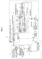
- Fig. 3 is a block diagram showing a transmitting electric power control apparatus using the S/N measuring circuit 10 in Fig. 1.
- a base station 20 includes an A/D converter 2, an S/N measuring circuit 10, a demodulator 11 connected to an antenna, a decoder 12, an adder 13, a decision device 14, a TPC bit generating circuit 15, and a transmitter 16 connected to an antenna.
- a mobile station 53 like the prior art includes a demodulator 21, a TPC bit decoder 22, a transmitting electric power determining circuit 23, a transmitter 24, and an encoder 25.
- the S/N measuring circuit 10 shown in Fig. 1 has the same arrangement as the S/N measuring circuit 10 shown in Fig. 1, and has a function in which a corrected and accurate S/N value is measured from the sampled value of the demodulated signal and output.
- the adder 13 a difference between a measured S/N that is an output from the S/N measuring circuit 10 and a preset control target S/N of transmitting electric power is calculated and supplied to the decision device 14.
- the decision device 14 determines an amount of increase or decrease of the transmitting electric power to the mobile station 53, based on an output from the adder 13.
- the determined amount of the increase or decrease of the transmitting electric power is converted into a bit by the TPC bit generating circuit 15, and is transmitted to the mobile station 20 by the transmitter 16.
- the demodulator 21 receives a signal transmitted by the base station and conducts demodulation.
- a demodulated signal that is an output from the demodulator 21 is input to the TPC bit decoder 22, and the TPC bit decoder decodes the TPC bit generated in the base station 20.
- the TPC bit decoded in the TPC bit decoder 22 is input to the transmitting electric power determining circuit 23, and transmitting electric power of the mobile station 53 is determined.
- the transmitter 24 transmits a coded information signal.
- non-linear bias characteristic in the S/N measurement is previously obtained by measurement, the conversion table for realizing this reverse characteristic is created, and when a measured S/N value is output from the dividing circuit, the table conversion circuit receives this S/N value as an input and outputs a corrected S/N value from the above-described conversion table. Therefore, it is possible to provide the S/N measuring circuit capable of measuring the S/N with high accuracy.
- the above-described corrected and measured S/N is compared with the target S/N in the base station, and the base station transmits a demand for increasing and decreasing the transmitting electric power to the mobile station, and, in accordance with the instruction from the base station, the transmitting electric power is determined in the mobile station.
- the apparatus since the outer-loop for correcting an S/N measuring bias is not necessary, a scale of the apparatus becomes to be small. Also, since the apparatus can cope with a fast change of the received S/N, it is possible to provide the transmitting electric power control apparatus capable of conducting the transmitting electric power control with high accuracy.
Abstract
Description

Claims (8)
- An S/N measuring circuit comprising:a modulation removing circuit, connected to an A/D converter for receiving a signal demodulated from a digital modulated signal and sampling said demodulated signal at a modulation clock, for removing data modulation by multiplying a sampled value of a demodulated signal that is an output from said A/D converter by a decision symbol signal;a first averaging circuit for averaging an output from said modulation removing circuit over a plurality of symbol sections to suppress a noise superimposed over said demodulated signal;a first square operating circuit for squaring an output from said first averaging circuit to obtain a desired signal power;a second square operating circuit for applying square operation to said sampled value of said demodulated signal that is an output from said A/D converter;a second averaging circuit for averaging an output from said second square operating circuit over a plurality of symbol sections to obtain total electric power of said demodulated signal;a subtracting circuit for subtracting said desired signal power that is an output from said first square operating circuit from said total electric power of said demodulated signal that is an output from said second averaging circuit to obtain noise electric power;a dividing circuit for receiving said desired signal power that is an output from said first square operating circuit and said noise electric power that is an output from said subtracting circuit, and calculating an S/N value; anda table conversion circuit for receiving said S/N value output from said dividing circuit and outputting an S/N value corrected in accordance with a predetermined conversion table.
- An S/N measuring circuit according to claim 1, wherein said table conversion circuit removes a non-linear bias occurred from a symbol error in case that said S/N value output from said dividing circuit is small by providing characteristic by means of said conversion table, which is reverse of characteristic previously obtained by measurement of a corresponding relation between said S/N value output from said dividing circuit and an actual S/N value of said demodulated signal.
- A transmitting electric power control apparatus for controlling transmitting electric power of an information signal transmitted to a base station from a mobile station, wherein
said base station comprises:and whereina demodulator for receiving a digital modulated and coded information signal and conducting demodulation;an A/D converter for sampling an output from said demodulator at a modulation clock;a decoder for decoding a demodulated signal that is an output from said A/D converter and outputting an information signal;a modulation removing circuit for removing data modulation by multiplying a sampled value of said demodulated signal that is an output from said A/D converter by a decision symbol signal;a first averaging circuit for averaging an output from said modulation removing circuit over a plurality of symbol sections to suppress a noise superimposed over said demodulated signal;a first square operating circuit for squaring an output from said first averaging circuit to obtain a desired signal power;a second square operating circuit for applying square operation to said sampled value of said demodulated signal that is an output from said A/D converter:a second averaging circuit for averaging an output from said second square operating circuit over a plurality of symbol sections to obtain total electric power of said demodulated signal;a subtracting circuit for subtracting said desired signal power that is an output from said first square operating circuit from said total electric power of said demodulated signal that is an output from said second averaging circuit to obtain noise electric power;a dividing circuit for receiving said desired signal power that is an output from said first square operating circuit and said noise electric power that is an output from said subtracting circuit, and obtaining an S/N value;a table conversion circuit for receiving said S/N value output from said dividing circuit and outputting an S/N value corrected in accordance with a predetermined conversion table;an adder for obtaining a difference between a measured S/N that is an output from said table conversion circuit and a target S/N that is a control target value of transmitting electric power;a decision device for determining an amount of increase or decrease of said transmitting electric power, which is instructed to said mobile station, from said difference between said measured S/N and said target S/N, which is an output from said adder;a TPC bit generating circuit for converting an output result from said decision device into a bit; anda transmitter for transmitting a TPC bit determined in said TPC bit generating circuit to said mobile station,
said mobile station comprises:a demodulator for receiving a digital modulated TPC signal and conducting demodulation;a TPC bit decoder for deciding a TPC bit from an output from said demodulator;a transmitting electric power determining circuit for receiving said TPC bit that is an output from said TPC bit decoder and determining transmitting electric power of said mobile station; anda transmitter for transmitting a coded information signal based on said transmitting electric power determined by said transmitting electric power determining circuit. - A transmitting electric power control apparatus according to claim 3, wherein said table conversion circuit removes a non-linear bias occurred from a symbol error in case that said S/N value output from said dividing circuit is small by providing characteristic by means of said conversion table, which is reverse of characteristic previously obtained by measurement of a corresponding relation between said S/N value output from said dividing circuit and an actual S/N value of said demodulated signal.
- A base station of a digital mobile communicating system for conducting communication while controlling transmitting electric power of an information signal transmitted to said base station from a mobile station, said base station comprising:a demodulator for receiving a digital modulated and coded information signal and conducting demodulation;an A/D converter for sampling an output from said demodulator at a modulation clock;a decoder for decoding a demodulated signal that is an output from said A/D converter and outputting an information signal;a modulation removing circuit for removing data modulation by multiplying a sampled value of said demodulated signal that is an output from said A/D converter by a decision symbol signal:a first averaging circuit for averaging an output from said modulation removing circuit over a plurality of symbol sections to suppress a noise superimposed over said demodulated signal;a first square operating circuit for squaring an output from said first averaging circuit to obtain a desired signal power;a second square operating circuit for applying square operation to said sampled value of said demodulated signal that is an output from said A/D converter;a second averaging circuit for averaging an output from said second square operating circuit over a plurality of symbol sections to obtain total electric power of said demodulated signal;a subtracting circuit for subtracting said desired signal power that is an output from said first square operating circuit from said total electric power of said demodulated signal that is an output from said second averaging circuit to obtain noise electric power;a dividing circuit for receiving said desired signal power that is an output from said first square operating circuit and said noise electric power that is an output from said subtracting circuit, and obtaining an S/N value;a table conversion circuit for receiving said S/N value output from said dividing circuit and outputting an S/N value corrected in accordance with a predetermined conversion table;an adder for obtaining a difference between a measured S/N that is an output from said table conversion circuit and a target S/N that is a control target value of transmitting electric power;a decision device for determining an amount of increase or decrease of said transmitting electric power, which is instructed to said mobile station, from said difference between said measured S/N and said target S/N, which is an output from said adder;a TPC bit generating circuit for converting an output result from said decision device into a bit; anda transmitter for transmitting a TPC bit determined in said TPC bit generating circuit to said mobile station.
- A digital mobile communicating system comprising:whereina base station recited in claim 5; anda mobile station recited in claim 5,
said mobile station includes:a demodulator for receiving a digital modulated TPC signal and conducting demodulation;a TPC bit decoder for deciding a TPC bit from an output from said demodulator;a transmitting electric power determining circuit for receiving said TPC bit that is an output from said TPC bit decoder and determining transmitting electric power of said mobile station; anda transmitter for transmitting a coded information signal based on said transmitting electric power determined by said transmitting electric power determining circuit. - An S/N measuring method comprising steps of:(a) removing data modulation by multiplying a sampled value of a demodulated signal that is an output from an A/D converter by a decision symbol signal, said A/D converter receiving a signal demodulated from a digital modulated signal and sampling said demodulated signal at a modulation clock;(b) averaging said demodulated signal in which said data modulation is removed, over a plurality of symbol sections to suppress a noise superimposed over said demodulated signal;(c) squaring said averaged signal to obtain a desired signal power;(d) applying square operation to said sampled value of said demodulated signal that is an output from said A/D converter;(e) averaging said squared value over a plurality of symbol sections to obtain total electric power of said demodulated signal;(f) subtracting said desired signal power from said total electric power to obtain noise electric power;(g) receiving said desired signal power and said noise electric power, and calculating an S/N value; and(h) receiving said S/N value and outputting an S/N value corrected in accordance with a predetermined conversion table.
- An S/N measuring method according to claim 7, wherein said step (h) includes a step of removing a non-linear bias occurred from a symbol error in case that said S/N value is small by providing characteristic by means of said conversion table, which is reverse of characteristic previously obtained by measurement of a corresponding relation between said S/N value and an actual S/N value of said demodulated signal.
Applications Claiming Priority (3)
| Application Number | Priority Date | Filing Date | Title |
|---|---|---|---|
| JP09186388A JP3132427B2 (en) | 1997-07-11 | 1997-07-11 | S / N measurement circuit, transmission power control device, and digital communication system |
| JP186388/97 | 1997-07-11 | ||
| JP18638897 | 1997-07-11 |
Publications (3)
| Publication Number | Publication Date |
|---|---|
| EP0890845A2 true EP0890845A2 (en) | 1999-01-13 |
| EP0890845A3 EP0890845A3 (en) | 2000-11-15 |
| EP0890845B1 EP0890845B1 (en) | 2004-02-18 |
Family
ID=16187528
Family Applications (1)
| Application Number | Title | Priority Date | Filing Date |
|---|---|---|---|
| EP19980112863 Expired - Lifetime EP0890845B1 (en) | 1997-07-11 | 1998-07-10 | Signal/Noise measuring circuit and method |
Country Status (5)
| Country | Link |
|---|---|
| US (1) | US6487174B1 (en) |
| EP (1) | EP0890845B1 (en) |
| JP (1) | JP3132427B2 (en) |
| CA (1) | CA2243133C (en) |
| DE (1) | DE69821684D1 (en) |
Cited By (3)
| Publication number | Priority date | Publication date | Assignee | Title |
|---|---|---|---|---|
| EP1460789A1 (en) * | 2003-03-21 | 2004-09-22 | Telefonaktiebolaget LM Ericsson (publ) | Method and apparatus for link adaptation |
| WO2004084452A2 (en) * | 2003-03-21 | 2004-09-30 | Telefonaktiebolaget L M Ericsson (Publ) | Method and apparatus for link adaptation |
| EP1062742B1 (en) * | 1998-03-11 | 2008-01-23 | Telefonaktiebolaget LM Ericsson (publ) | Correction of signal-interference ratio measures |
Families Citing this family (11)
| Publication number | Priority date | Publication date | Assignee | Title |
|---|---|---|---|---|
| JP3358565B2 (en) * | 1998-11-02 | 2002-12-24 | 日本電気株式会社 | Transmission power control method, transmission power control device, mobile station, base station, and control station |
| US6490461B1 (en) * | 1999-06-24 | 2002-12-03 | Telefonaktiebolaget Lm Ericsson (Publ) | Power control based on combined quality estimates |
| US6678312B1 (en) * | 1999-12-22 | 2004-01-13 | Koninklijke Philips Electronics N.V. | Method for extending digital receiver sensitivity using analog correlation |
| JP3573073B2 (en) * | 2000-08-09 | 2004-10-06 | 日本電気株式会社 | Transmission power control system and transmission power control method used therefor |
| CA2323164A1 (en) * | 2000-10-11 | 2002-04-11 | Ramesh Mantha | Method, system and apparatus for improving reception in multiple access communication systems |
| US6850499B2 (en) * | 2001-01-05 | 2005-02-01 | Qualcomm Incorporated | Method and apparatus for forward power control in a communication system |
| TWI371925B (en) * | 2006-09-08 | 2012-09-01 | Via Tech Inc | Apparatus for processing multiple signals with a single analog-to-digital converter and method thereof |
| US8054872B2 (en) * | 2007-06-21 | 2011-11-08 | O2Micro, Inc. | Method and apparatus for signal carrier-to-noise power density ratio calculation |
| RU2466416C1 (en) * | 2011-05-06 | 2012-11-10 | Открытое акционерное общество "Концерн "Океанприбор" | Method of measuring signal-to-noise ratio |
| US9270369B2 (en) * | 2014-01-13 | 2016-02-23 | Fujitsu Limited | Correction table for interferometric optical signal-to-noise ratio monitor |
| RU2598693C1 (en) * | 2015-03-25 | 2016-09-27 | ООО "Топкон Позишионинг Системс" | Method and apparatus for estimating current signal-noise ratio |
Citations (2)
| Publication number | Priority date | Publication date | Assignee | Title |
|---|---|---|---|---|
| US4941199A (en) * | 1989-04-06 | 1990-07-10 | Scientific Atlanta | Uplink power control mechanism for maintaining constant output power from satellite transponder |
| US5278992A (en) * | 1991-11-08 | 1994-01-11 | Teknekron Communications Systems, Inc. | Method and apparatus for controlling transmission power of a remote unit communicating with a base unit over a common frequency channel |
Family Cites Families (5)
| Publication number | Priority date | Publication date | Assignee | Title |
|---|---|---|---|---|
| JPH0676925B2 (en) | 1990-06-20 | 1994-09-28 | 日本アビオニクス株式会社 | Temperature measurement method |
| FR2710214B1 (en) * | 1993-09-15 | 1995-10-20 | Alcatel Mobile Comm France | Threshold detector for a digital radio transmission system, devices comprising such a threshold detector and corresponding use. |
| US5603096A (en) * | 1994-07-11 | 1997-02-11 | Qualcomm Incorporated | Reverse link, closed loop power control in a code division multiple access system |
| US5450453A (en) * | 1994-09-28 | 1995-09-12 | Motorola, Inc. | Method, apparatus and system for decoding a non-coherently demodulated signal |
| JP2785804B2 (en) * | 1996-05-30 | 1998-08-13 | 日本電気株式会社 | Mobile communication system |
-
1997
- 1997-07-11 JP JP09186388A patent/JP3132427B2/en not_active Expired - Fee Related
-
1998
- 1998-07-10 DE DE69821684T patent/DE69821684D1/en not_active Expired - Lifetime
- 1998-07-10 EP EP19980112863 patent/EP0890845B1/en not_active Expired - Lifetime
- 1998-07-10 CA CA 2243133 patent/CA2243133C/en not_active Expired - Fee Related
- 1998-07-10 US US09/113,219 patent/US6487174B1/en not_active Expired - Lifetime
Patent Citations (2)
| Publication number | Priority date | Publication date | Assignee | Title |
|---|---|---|---|---|
| US4941199A (en) * | 1989-04-06 | 1990-07-10 | Scientific Atlanta | Uplink power control mechanism for maintaining constant output power from satellite transponder |
| US5278992A (en) * | 1991-11-08 | 1994-01-11 | Teknekron Communications Systems, Inc. | Method and apparatus for controlling transmission power of a remote unit communicating with a base unit over a common frequency channel |
Cited By (4)
| Publication number | Priority date | Publication date | Assignee | Title |
|---|---|---|---|---|
| EP1062742B1 (en) * | 1998-03-11 | 2008-01-23 | Telefonaktiebolaget LM Ericsson (publ) | Correction of signal-interference ratio measures |
| EP1460789A1 (en) * | 2003-03-21 | 2004-09-22 | Telefonaktiebolaget LM Ericsson (publ) | Method and apparatus for link adaptation |
| WO2004084452A2 (en) * | 2003-03-21 | 2004-09-30 | Telefonaktiebolaget L M Ericsson (Publ) | Method and apparatus for link adaptation |
| WO2004084452A3 (en) * | 2003-03-21 | 2008-01-17 | Ericsson Telefon Ab L M | Method and apparatus for link adaptation |
Also Published As
| Publication number | Publication date |
|---|---|
| JP3132427B2 (en) | 2001-02-05 |
| DE69821684D1 (en) | 2004-03-25 |
| EP0890845A3 (en) | 2000-11-15 |
| CA2243133A1 (en) | 1999-01-11 |
| US6487174B1 (en) | 2002-11-26 |
| EP0890845B1 (en) | 2004-02-18 |
| JPH1132092A (en) | 1999-02-02 |
| CA2243133C (en) | 2003-09-09 |
Similar Documents
| Publication | Publication Date | Title |
|---|---|---|
| EP0890845B1 (en) | Signal/Noise measuring circuit and method | |
| JP2923867B2 (en) | Transmission power control method | |
| AU713270B2 (en) | Digital calibration of a transceiver | |
| WO2001022756A1 (en) | Transmission power controller | |
| KR20000006067A (en) | Digital automatic gain control linearizer and digital automatic gain control circuit using the same | |
| EP1128572B1 (en) | A method of adjusting a signal quality target during transmission power control in a CDMA radio communication network | |
| EP1071227B1 (en) | CDMA reception apparatus and received signal power measuring apparatus in CDMA mobile communication system | |
| US6556839B1 (en) | Apparatus for and method of controlling transmission power | |
| JP4257058B2 (en) | WIRELESS COMMUNICATION SYSTEM, RECEIVING FIELD INTENSITY COMPENSATION METHOD IN WIRELESS COMMUNICATION SYSTEM, BASE STATION AND TERMINAL STATION FOR WIRELESS COMMUNICATION SYSTEM | |
| EP0924875B1 (en) | Diversity reception method and apparatus in a CDMA system | |
| US6724808B1 (en) | Transmission power control method of measuring Eb/N0 after weighted signals are combined | |
| US20060245524A1 (en) | Radio receiver with a demodulation unit for generating softbits | |
| EP0405384B1 (en) | Apparatus for estimating communication link quality | |
| CA2413934C (en) | S/n measuring circuit and method, transmitting electric power control apparatus and digital communicating system | |
| US7978786B2 (en) | Apparatus and method for quantization in digital communication system | |
| US20080194297A1 (en) | Sir Determining Apparatus and Wireless Communication Apparatus | |
| JP2001339455A (en) | Reception device and radio communication device | |
| JP3403566B2 (en) | Demodulator | |
| KR100666985B1 (en) | Method and apparatus for calibrating in adaptive array antenna system | |
| KR100338670B1 (en) | Apparatus for controlling power of sending signal in wireless local loop of wide-band cdma | |
| US20140355654A1 (en) | Radio Receiver for Detecting an Additive White Gaussian Noise Channel | |
| US7532905B2 (en) | Filter device and transmission power control apparatus | |
| KR100326307B1 (en) | Apparatus and method for symbol normalizing in cdma system | |
| JPS62178024A (en) | Transmission power controller for satellite communication earth station | |
| KR20010084467A (en) | Adaptive coherent demodulation system for mobile communication system |
Legal Events
| Date | Code | Title | Description |
|---|---|---|---|
| PUAI | Public reference made under article 153(3) epc to a published international application that has entered the european phase |
Free format text: ORIGINAL CODE: 0009012 |
|
| AK | Designated contracting states |
Kind code of ref document: A2 Designated state(s): DE FI FR GB IT SE |
|
| AX | Request for extension of the european patent |
Free format text: AL;LT;LV;MK;RO;SI |
|
| PUAL | Search report despatched |
Free format text: ORIGINAL CODE: 0009013 |
|
| AK | Designated contracting states |
Kind code of ref document: A3 Designated state(s): AT BE CH CY DE DK ES FI FR GB GR IE IT LI LU MC NL PT SE |
|
| AX | Request for extension of the european patent |
Free format text: AL;LT;LV;MK;RO;SI |
|
| RIC1 | Information provided on ipc code assigned before grant |
Free format text: 7G 01R 29/26 A, 7H 04B 7/26 B |
|
| 17P | Request for examination filed |
Effective date: 20001012 |
|
| AKX | Designation fees paid |
Free format text: DE FI FR GB IT SE |
|
| 17Q | First examination report despatched |
Effective date: 20021218 |
|
| GRAP | Despatch of communication of intention to grant a patent |
Free format text: ORIGINAL CODE: EPIDOSNIGR1 |
|
| RTI1 | Title (correction) |
Free format text: SIGNAL/NOISE MEASURING CIRCUIT AND METHOD |
|
| RTI1 | Title (correction) |
Free format text: SIGNAL/NOISE MEASURING CIRCUIT AND METHOD |
|
| GRAS | Grant fee paid |
Free format text: ORIGINAL CODE: EPIDOSNIGR3 |
|
| GRAA | (expected) grant |
Free format text: ORIGINAL CODE: 0009210 |
|
| AK | Designated contracting states |
Kind code of ref document: B1 Designated state(s): DE FI FR GB IT SE |
|
| PG25 | Lapsed in a contracting state [announced via postgrant information from national office to epo] |
Ref country code: IT Free format text: LAPSE BECAUSE OF FAILURE TO SUBMIT A TRANSLATION OF THE DESCRIPTION OR TO PAY THE FEE WITHIN THE PRE;WARNING: LAPSES OF ITALIAN PATENTS WITH EFFECTIVE DATE BEFORE 2007 MAY HAVE OCCURRED AT ANY TIME BEFORE 2007. THE CORRECT EFFECTIVE DATE MAY BE DIFFERENT FROM THE ONE RECORDED.SCRIBED TIME-LIMIT Effective date: 20040218 Ref country code: FR Free format text: LAPSE BECAUSE OF FAILURE TO SUBMIT A TRANSLATION OF THE DESCRIPTION OR TO PAY THE FEE WITHIN THE PRESCRIBED TIME-LIMIT Effective date: 20040218 Ref country code: FI Free format text: LAPSE BECAUSE OF FAILURE TO SUBMIT A TRANSLATION OF THE DESCRIPTION OR TO PAY THE FEE WITHIN THE PRESCRIBED TIME-LIMIT Effective date: 20040218 |
|
| REG | Reference to a national code |
Ref country code: GB Ref legal event code: FG4D |
|
| REF | Corresponds to: |
Ref document number: 69821684 Country of ref document: DE Date of ref document: 20040325 Kind code of ref document: P |
|
| PG25 | Lapsed in a contracting state [announced via postgrant information from national office to epo] |
Ref country code: SE Free format text: LAPSE BECAUSE OF FAILURE TO SUBMIT A TRANSLATION OF THE DESCRIPTION OR TO PAY THE FEE WITHIN THE PRESCRIBED TIME-LIMIT Effective date: 20040518 |
|
| PG25 | Lapsed in a contracting state [announced via postgrant information from national office to epo] |
Ref country code: DE Free format text: LAPSE BECAUSE OF FAILURE TO SUBMIT A TRANSLATION OF THE DESCRIPTION OR TO PAY THE FEE WITHIN THE PRESCRIBED TIME-LIMIT Effective date: 20040519 |
|
| PLBE | No opposition filed within time limit |
Free format text: ORIGINAL CODE: 0009261 |
|
| STAA | Information on the status of an ep patent application or granted ep patent |
Free format text: STATUS: NO OPPOSITION FILED WITHIN TIME LIMIT |
|
| EN | Fr: translation not filed | ||
| 26N | No opposition filed |
Effective date: 20041119 |
|
| PGFP | Annual fee paid to national office [announced via postgrant information from national office to epo] |
Ref country code: GB Payment date: 20130710 Year of fee payment: 16 |
|
| GBPC | Gb: european patent ceased through non-payment of renewal fee |
Effective date: 20140710 |
|
| PG25 | Lapsed in a contracting state [announced via postgrant information from national office to epo] |
Ref country code: GB Free format text: LAPSE BECAUSE OF NON-PAYMENT OF DUE FEES Effective date: 20140710 |