EP0891121B1 - Organic electroluminescent elements - Google Patents
Organic electroluminescent elements Download PDFInfo
- Publication number
- EP0891121B1 EP0891121B1 EP97950436A EP97950436A EP0891121B1 EP 0891121 B1 EP0891121 B1 EP 0891121B1 EP 97950436 A EP97950436 A EP 97950436A EP 97950436 A EP97950436 A EP 97950436A EP 0891121 B1 EP0891121 B1 EP 0891121B1
- Authority
- EP
- European Patent Office
- Prior art keywords
- compound
- substition
- organic
- layer
- injecting
- Prior art date
- Legal status (The legal status is an assumption and is not a legal conclusion. Google has not performed a legal analysis and makes no representation as to the accuracy of the status listed.)
- Expired - Lifetime
Links
- WTQXGXFDLZBWJI-UHFFFAOYSA-N Cc1cccc(N(C)c2ccccc2)c1 Chemical compound Cc1cccc(N(C)c2ccccc2)c1 WTQXGXFDLZBWJI-UHFFFAOYSA-N 0.000 description 7
- ULSJAOPJTJDYGP-UHFFFAOYSA-N Cc(cc1)ccc1N(C)c1ccccc1 Chemical compound Cc(cc1)ccc1N(C)c1ccccc1 ULSJAOPJTJDYGP-UHFFFAOYSA-N 0.000 description 6
- IXPHIYGRFBMTLJ-UHFFFAOYSA-N Cc(cc1)ccc1N(C)c1ccc(C)cc1 Chemical compound Cc(cc1)ccc1N(C)c1ccc(C)cc1 IXPHIYGRFBMTLJ-UHFFFAOYSA-N 0.000 description 5
- FWAOJONKONPYIH-UHFFFAOYSA-N CN(c1ccccc1)c1cc(OC)ccc1 Chemical compound CN(c1ccccc1)c1cc(OC)ccc1 FWAOJONKONPYIH-UHFFFAOYSA-N 0.000 description 3
- NUWYSMKROCSTLW-UHFFFAOYSA-N Cc1cccc(N(c2ccccc2)c(cc2)ccc2N(C)c2ccccc2)c1 Chemical compound Cc1cccc(N(c2ccccc2)c(cc2)ccc2N(C)c2ccccc2)c1 NUWYSMKROCSTLW-UHFFFAOYSA-N 0.000 description 2
- YXFVVABEGXRONW-UHFFFAOYSA-N Cc1ccccc1 Chemical compound Cc1ccccc1 YXFVVABEGXRONW-UHFFFAOYSA-N 0.000 description 2
- KOLTUBXBRZRUQK-UHFFFAOYSA-N CC(C#C1)=CCC1N(C1=C=CC#CC1)c(cc1)ccc1N(C)c1ccccc1 Chemical compound CC(C#C1)=CCC1N(C1=C=CC#CC1)c(cc1)ccc1N(C)c1ccccc1 KOLTUBXBRZRUQK-UHFFFAOYSA-N 0.000 description 1
- JOIYYFWCKREFBO-UHFFFAOYSA-N CC(C1)C=CC=C1N(C)c1ccccc1 Chemical compound CC(C1)C=CC=C1N(C)c1ccccc1 JOIYYFWCKREFBO-UHFFFAOYSA-N 0.000 description 1
- XQERZFFCDQMEFJ-UHFFFAOYSA-N CC(C=C1)=CCC1N(C)c1ccccc1 Chemical compound CC(C=C1)=CCC1N(C)c1ccccc1 XQERZFFCDQMEFJ-UHFFFAOYSA-N 0.000 description 1
- BKOFDBQMGKMPON-UHFFFAOYSA-N CC(C=C1)=CCC1N(c1ccccc1)c(cc1)ccc1N(C)c1ccccc1 Chemical compound CC(C=C1)=CCC1N(c1ccccc1)c(cc1)ccc1N(C)c1ccccc1 BKOFDBQMGKMPON-UHFFFAOYSA-N 0.000 description 1
- RJYIUSUKASSXGY-UHFFFAOYSA-N CN(c(cc1)ccc1Oc1ccccc1)c(cc1)ccc1Oc1ccccc1 Chemical compound CN(c(cc1)ccc1Oc1ccccc1)c(cc1)ccc1Oc1ccccc1 RJYIUSUKASSXGY-UHFFFAOYSA-N 0.000 description 1
- JYNABQRMIKWGTK-UHFFFAOYSA-N CN(c1ccccc1)c(cc1)ccc1OC Chemical compound CN(c1ccccc1)c(cc1)ccc1OC JYNABQRMIKWGTK-UHFFFAOYSA-N 0.000 description 1
- VFNMUKURWPRPRQ-UHFFFAOYSA-N CN(c1ccccc1)c1ccccc1OC Chemical compound CN(c1ccccc1)c1ccccc1OC VFNMUKURWPRPRQ-UHFFFAOYSA-N 0.000 description 1
- AFBPFSWMIHJQDM-UHFFFAOYSA-N CNc1ccccc1 Chemical compound CNc1ccccc1 AFBPFSWMIHJQDM-UHFFFAOYSA-N 0.000 description 1
- WZPRWPWDNPXABO-UHFFFAOYSA-N Cc(cc1)ccc1N(C)c(cc1)ccc1N(c1ccc(C)cc1)c1cccc(C)c1 Chemical compound Cc(cc1)ccc1N(C)c(cc1)ccc1N(c1ccc(C)cc1)c1cccc(C)c1 WZPRWPWDNPXABO-UHFFFAOYSA-N 0.000 description 1
- KESYBVGPAYXCHQ-UHFFFAOYSA-N Cc(cc1)ccc1N(c1ccc(C)cc1)c(cc1)ccc1N(C)c1ccccc1 Chemical compound Cc(cc1)ccc1N(c1ccc(C)cc1)c(cc1)ccc1N(C)c1ccccc1 KESYBVGPAYXCHQ-UHFFFAOYSA-N 0.000 description 1
- JFFWDKQNHWNUNS-UHFFFAOYSA-N Cc1cc(N(c2ccccc2)c(cc2)ccc2N(C)c(cc2)ccc2N(C2C=CC=CC2)c2cc3ccccc3cc2)ccc1 Chemical compound Cc1cc(N(c2ccccc2)c(cc2)ccc2N(C)c(cc2)ccc2N(C2C=CC=CC2)c2cc3ccccc3cc2)ccc1 JFFWDKQNHWNUNS-UHFFFAOYSA-N 0.000 description 1
- PQUBCDKLHZRPNL-UHFFFAOYSA-N Cc1cccc(N(C)c2cc(C)ccc2)c1 Chemical compound Cc1cccc(N(C)c2cc(C)ccc2)c1 PQUBCDKLHZRPNL-UHFFFAOYSA-N 0.000 description 1
- QIAOWMLMPPNSPG-UHFFFAOYSA-N Cc1cccc(N(C2C=CC(N(C)s3ccccc3)=CC2)c2cc(C)ccc2)c1 Chemical compound Cc1cccc(N(C2C=CC(N(C)s3ccccc3)=CC2)c2cc(C)ccc2)c1 QIAOWMLMPPNSPG-UHFFFAOYSA-N 0.000 description 1
- WXDNOIHQSYEXGY-UHFFFAOYSA-N Cc1cccc(N(c(cc2)ccc2N(C)c2ccccc2)c2cccc(C)c2)c1 Chemical compound Cc1cccc(N(c(cc2)ccc2N(C)c2ccccc2)c2cccc(C)c2)c1 WXDNOIHQSYEXGY-UHFFFAOYSA-N 0.000 description 1
Images


Classifications
-
- H—ELECTRICITY
- H05—ELECTRIC TECHNIQUES NOT OTHERWISE PROVIDED FOR
- H05B—ELECTRIC HEATING; ELECTRIC LIGHT SOURCES NOT OTHERWISE PROVIDED FOR; CIRCUIT ARRANGEMENTS FOR ELECTRIC LIGHT SOURCES, IN GENERAL
- H05B33/00—Electroluminescent light sources
- H05B33/12—Light sources with substantially two-dimensional radiating surfaces
- H05B33/14—Light sources with substantially two-dimensional radiating surfaces characterised by the chemical or physical composition or the arrangement of the electroluminescent material, or by the simultaneous addition of the electroluminescent material in or onto the light source
-
- C—CHEMISTRY; METALLURGY
- C09—DYES; PAINTS; POLISHES; NATURAL RESINS; ADHESIVES; COMPOSITIONS NOT OTHERWISE PROVIDED FOR; APPLICATIONS OF MATERIALS NOT OTHERWISE PROVIDED FOR
- C09K—MATERIALS FOR MISCELLANEOUS APPLICATIONS, NOT PROVIDED FOR ELSEWHERE
- C09K11/00—Luminescent, e.g. electroluminescent, chemiluminescent materials
- C09K11/06—Luminescent, e.g. electroluminescent, chemiluminescent materials containing organic luminescent materials
-
- H—ELECTRICITY
- H05—ELECTRIC TECHNIQUES NOT OTHERWISE PROVIDED FOR
- H05B—ELECTRIC HEATING; ELECTRIC LIGHT SOURCES NOT OTHERWISE PROVIDED FOR; CIRCUIT ARRANGEMENTS FOR ELECTRIC LIGHT SOURCES, IN GENERAL
- H05B33/00—Electroluminescent light sources
- H05B33/12—Light sources with substantially two-dimensional radiating surfaces
-
- H—ELECTRICITY
- H10—SEMICONDUCTOR DEVICES; ELECTRIC SOLID-STATE DEVICES NOT OTHERWISE PROVIDED FOR
- H10K—ORGANIC ELECTRIC SOLID-STATE DEVICES
- H10K50/00—Organic light-emitting devices
- H10K50/10—OLEDs or polymer light-emitting diodes [PLED]
- H10K50/11—OLEDs or polymer light-emitting diodes [PLED] characterised by the electroluminescent [EL] layers
-
- H—ELECTRICITY
- H10—SEMICONDUCTOR DEVICES; ELECTRIC SOLID-STATE DEVICES NOT OTHERWISE PROVIDED FOR
- H10K—ORGANIC ELECTRIC SOLID-STATE DEVICES
- H10K85/00—Organic materials used in the body or electrodes of devices covered by this subclass
- H10K85/60—Organic compounds having low molecular weight
- H10K85/615—Polycyclic condensed aromatic hydrocarbons, e.g. anthracene
-
- H—ELECTRICITY
- H10—SEMICONDUCTOR DEVICES; ELECTRIC SOLID-STATE DEVICES NOT OTHERWISE PROVIDED FOR
- H10K—ORGANIC ELECTRIC SOLID-STATE DEVICES
- H10K85/00—Organic materials used in the body or electrodes of devices covered by this subclass
- H10K85/60—Organic compounds having low molecular weight
- H10K85/631—Amine compounds having at least two aryl rest on at least one amine-nitrogen atom, e.g. triphenylamine
- H10K85/633—Amine compounds having at least two aryl rest on at least one amine-nitrogen atom, e.g. triphenylamine comprising polycyclic condensed aromatic hydrocarbons as substituents on the nitrogen atom
-
- C—CHEMISTRY; METALLURGY
- C09—DYES; PAINTS; POLISHES; NATURAL RESINS; ADHESIVES; COMPOSITIONS NOT OTHERWISE PROVIDED FOR; APPLICATIONS OF MATERIALS NOT OTHERWISE PROVIDED FOR
- C09K—MATERIALS FOR MISCELLANEOUS APPLICATIONS, NOT PROVIDED FOR ELSEWHERE
- C09K2211/00—Chemical nature of organic luminescent or tenebrescent compounds
- C09K2211/10—Non-macromolecular compounds
- C09K2211/1003—Carbocyclic compounds
- C09K2211/1007—Non-condensed systems
-
- C—CHEMISTRY; METALLURGY
- C09—DYES; PAINTS; POLISHES; NATURAL RESINS; ADHESIVES; COMPOSITIONS NOT OTHERWISE PROVIDED FOR; APPLICATIONS OF MATERIALS NOT OTHERWISE PROVIDED FOR
- C09K—MATERIALS FOR MISCELLANEOUS APPLICATIONS, NOT PROVIDED FOR ELSEWHERE
- C09K2211/00—Chemical nature of organic luminescent or tenebrescent compounds
- C09K2211/10—Non-macromolecular compounds
- C09K2211/1003—Carbocyclic compounds
- C09K2211/1011—Condensed systems
-
- C—CHEMISTRY; METALLURGY
- C09—DYES; PAINTS; POLISHES; NATURAL RESINS; ADHESIVES; COMPOSITIONS NOT OTHERWISE PROVIDED FOR; APPLICATIONS OF MATERIALS NOT OTHERWISE PROVIDED FOR
- C09K—MATERIALS FOR MISCELLANEOUS APPLICATIONS, NOT PROVIDED FOR ELSEWHERE
- C09K2211/00—Chemical nature of organic luminescent or tenebrescent compounds
- C09K2211/10—Non-macromolecular compounds
- C09K2211/1003—Carbocyclic compounds
- C09K2211/1014—Carbocyclic compounds bridged by heteroatoms, e.g. N, P, Si or B
-
- H—ELECTRICITY
- H10—SEMICONDUCTOR DEVICES; ELECTRIC SOLID-STATE DEVICES NOT OTHERWISE PROVIDED FOR
- H10K—ORGANIC ELECTRIC SOLID-STATE DEVICES
- H10K2102/00—Constructional details relating to the organic devices covered by this subclass
- H10K2102/10—Transparent electrodes, e.g. using graphene
- H10K2102/101—Transparent electrodes, e.g. using graphene comprising transparent conductive oxides [TCO]
- H10K2102/103—Transparent electrodes, e.g. using graphene comprising transparent conductive oxides [TCO] comprising indium oxides, e.g. ITO
-
- H—ELECTRICITY
- H10—SEMICONDUCTOR DEVICES; ELECTRIC SOLID-STATE DEVICES NOT OTHERWISE PROVIDED FOR
- H10K—ORGANIC ELECTRIC SOLID-STATE DEVICES
- H10K85/00—Organic materials used in the body or electrodes of devices covered by this subclass
- H10K85/30—Coordination compounds
- H10K85/321—Metal complexes comprising a group IIIA element, e.g. Tris (8-hydroxyquinoline) gallium [Gaq3]
- H10K85/324—Metal complexes comprising a group IIIA element, e.g. Tris (8-hydroxyquinoline) gallium [Gaq3] comprising aluminium, e.g. Alq3
-
- H—ELECTRICITY
- H10—SEMICONDUCTOR DEVICES; ELECTRIC SOLID-STATE DEVICES NOT OTHERWISE PROVIDED FOR
- H10K—ORGANIC ELECTRIC SOLID-STATE DEVICES
- H10K85/00—Organic materials used in the body or electrodes of devices covered by this subclass
- H10K85/60—Organic compounds having low molecular weight
- H10K85/615—Polycyclic condensed aromatic hydrocarbons, e.g. anthracene
- H10K85/622—Polycyclic condensed aromatic hydrocarbons, e.g. anthracene containing four rings, e.g. pyrene
-
- H—ELECTRICITY
- H10—SEMICONDUCTOR DEVICES; ELECTRIC SOLID-STATE DEVICES NOT OTHERWISE PROVIDED FOR
- H10K—ORGANIC ELECTRIC SOLID-STATE DEVICES
- H10K85/00—Organic materials used in the body or electrodes of devices covered by this subclass
- H10K85/60—Organic compounds having low molecular weight
- H10K85/615—Polycyclic condensed aromatic hydrocarbons, e.g. anthracene
- H10K85/623—Polycyclic condensed aromatic hydrocarbons, e.g. anthracene containing five rings, e.g. pentacene
-
- H—ELECTRICITY
- H10—SEMICONDUCTOR DEVICES; ELECTRIC SOLID-STATE DEVICES NOT OTHERWISE PROVIDED FOR
- H10K—ORGANIC ELECTRIC SOLID-STATE DEVICES
- H10K85/00—Organic materials used in the body or electrodes of devices covered by this subclass
- H10K85/60—Organic compounds having low molecular weight
- H10K85/615—Polycyclic condensed aromatic hydrocarbons, e.g. anthracene
- H10K85/626—Polycyclic condensed aromatic hydrocarbons, e.g. anthracene containing more than one polycyclic condensed aromatic rings, e.g. bis-anthracene
-
- Y—GENERAL TAGGING OF NEW TECHNOLOGICAL DEVELOPMENTS; GENERAL TAGGING OF CROSS-SECTIONAL TECHNOLOGIES SPANNING OVER SEVERAL SECTIONS OF THE IPC; TECHNICAL SUBJECTS COVERED BY FORMER USPC CROSS-REFERENCE ART COLLECTIONS [XRACs] AND DIGESTS
- Y10—TECHNICAL SUBJECTS COVERED BY FORMER USPC
- Y10S—TECHNICAL SUBJECTS COVERED BY FORMER USPC CROSS-REFERENCE ART COLLECTIONS [XRACs] AND DIGESTS
- Y10S428/00—Stock material or miscellaneous articles
- Y10S428/917—Electroluminescent
Definitions
- the present invention relates generally to an organic EL (electroluminescent) device, and specifically to a device which emits light upon the application of an electric field to a thin film of multilayered structure. More specifically, the present invention is concerned with an organic electroluminescent light emission device according to claim 1, so that low driving voltage, stable light emission, high quality display images and high heat resistance are achievable.
- organic EL electroluminescent
- An organic EL device comprises a thin film containing a fluorescent organic compound interleaved between an electron injecting electrode (cathode) and a hole injecting electrode (anode), and emits light making use of light emissions (fluorescence and phosphorescence) upon deactivation of excitons which are generated by injecting electrons and holes in the thin film for their recombination.
- organic EL device surface light emission of high luminance of the order of hundreds candelas/m 2 to scores of thousands of candelas/m 2 is achievable at a low voltage of up to 10 V, and blue to red light emissions are achievable by selecting the type of fluorescent material.
- An inhomogeneous organic thin film interface caused as by the growth of crystal domains is responsible for a drop of the ability of the device to inject holes, short-circuiting, and dielectric breakdown.
- crystal grains manifest themselves and grow greatly, resulting in a strikingly reduced film property.
- an organic thin film interface with ITO or the like is roughened, too, crystal grains manifest themselves and grow greatly, resulting in a light emission efficiency drop and current leakage which eventually lead to non-emission. This is also a leading cause of local non-emitting spots, i.e., dark spots.
- Na, K, Li, Mg, Ca, and Al has so far used as a metal having a low work function.
- these metals react with atmospheric moisture or oxygen or the organic layer peels off the electron injecting electrode, it is impossible co inject holes.
- solvent residues after film formation, moisture and decomposed products accelerate the oxidation reaction of the electrode, and causes the delamination of the electrode, resulting in local non-emitting spots.
- the generation of heat is unavoidable because a current is passed through the organic compound and so the organic compound must be placed in a high field strength. The heat then gives rise to the melting, crystallization, and thermal decomposition of the organic compound, resulting in a deterioration and breakdown of the device.
- the organic material Upon passing a current through the organic material, the organic material degrades, resulting in defects such as current or exciton traps. These defects in turn cause a deterioration of the device such as a driving voltage increase or a luminance drop.
- a hole or electron injecting electrode interface that is an interface between an organic material and an inorganic material, especially the hole injecting electrode interface has a great influence on the film property of the organic material layer during film formation. In some cases, several problems arise; an inhomogeneous organic layer is formed on the hole injecting electrode, and no good interface can be formed.
- Another object of the invention is to provide an organic EL device comprising an organic thin film formed by an evaporation technique of a compound that has high amorphism and high compatibility with a hole injecting electrode, said organic EL device being free from a driving voltage increase or a luminance drop and a current leakage with neither development nor growth of local non-emitting spots while it is driven, and so being capable of emitting light with high luminance, and high reliability such as high heat resistance.
- Yet another object of the invention is to provide an organic EL device using a multilayered film, said organic EL device comprising a hole injecting electrode or an organic material combined therewith, to which the optimum work function is imparted, and having high heat resistance.
- a further object of the invention is to provide an organic EL device capable of having high Hole mobility and so obtaining much higher current density.
- the organic EL device of the invention wherein the compound represented by formula (I) is used for a hole injecting layer or a hole injecting and transporting layer, it is possible to achieve consistent and uniform light emission due to an improved thin film property.
- the organic EL device of the invention also remains stable or uncrystallized over a period of 1 year or longer in the air.
- the aforesaid compound is characterized by having in its molecular structure a phenylenediamine skeleton to optimize hole injection efficiency and a benzidine skeleton (biphenyldiamine) and a skeleton having diamines with respect to a plurality of phenylenes to improve Hole mobility.
- the organic EL device of the invention can stand up to high-temperature driving, and can efficiently emit light at a low driving voltage and a small driving current. Furthermore, when the organic EL device of the invention is continuously driven, there is only a slight or limited increase in the driving voltage. It is here to be noted that the EL device of the invention has a light emission maximum wavelength of the order of 400 to 700 nm.
- the organic EL device of the invention comprises organic compound layers, at least one of which contains a compound having a skeleton represented by formula (1).
- L 0 stands for a set of phenylene groups. Included in the set of phenylene groups represented by formula (I) are o-phenylene and/or p-phenylene and/or m-phenylene. These phenylene groups may have a substituent. For instance, a biphenylene group represented as a phenylene group having two rings may include 4,4'-biphenylene, 3,3'-biphenylene and 3,4'-biphenylene groups among which the 4,4'-biphenylene group is particularly preferred.
- a terphenylene group represented as a phenylene group having three rings may include o-, p- and m-terphenylene groups among which the p-terphenylene (4,4',4''-terphenylene) group is particularly preferred.
- a quarter-phenylene group represented as a phenylene group having four rings may include o-, p- and m-quaterphenylene groups among which the p-quaterphenylene (4,4',4'',4'''-quaterphenylene) group is particularly preferred.
- a phenylene group having four rings may have a substituted or unsubstituted phenylamino group somewhere therein. As the substituent in this case, the same substituents as mentioned in conjunction with the following R 11 and R 12 may be used.
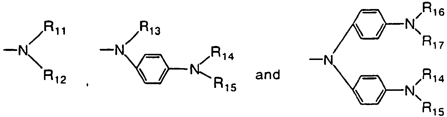
- R 01 , R 02 , R 03 and R 04 are each any one of the following groups: R 11 , R 12 , R 13 , R 14 , R 15 , R 16 and R 17 are each a substituted or unsubstituted aryl group.
- the aryl groups represented by R 11 , R 12 , R 13 , R 14 , R 15 , R 16 and R 17 may be a monocyclic or polycyclic aryl group, and have preferably 6 to 20 carbon atoms in all.
- aryl groups may further be substituted by an alkyl group having 1 to 6 carbon atoms, an unsubstituted or substituted aryl or alkoxy group, an aryloxy group, and the following group: where R 21 and R 22 are each an unsubstituted or substituted aryl group.
- the aryl group represented by R 21 , and R 22 is preferably a monocyclic or polycyclic aryl group having 6 to 20 carbon atoms in all.
- phenyl, naphthyl, anthryl, phenanthryl, pyrenyl, perylenyl, o-biphenyl, m-biphenyl, and p-biphenyl groups are mentioned, with the phenyl group being most preferred.
- These aryl groups may have a substituent such as an alkyl group having 1 to 6 carbon atoms, and an unsubstituted or substituted aryl group.
- a methyl group is preferably mentioned for the alkyl group, and a phenyl group is preferably mentioned for the aryl group.
- r 1 , r 2 , r 3 , and r 4 represents an integer of preferably 0 to 5, especially 0, 1 and 2, and most especially 0 or 1. It is then preferred that r 1 + r 2 + r 3 + r4 is at least 1, especially 1, 2, 3 or 4, and most especially 2, 3 or 4.
- R 01 , R 02 , R 03 , and R 04 bonds to the meta- or para-position with respect to the N bond position; R 01 , R 02 , R 03 and R 04 may all bond to the meta-positions, R 01 , R 02 , R 03 and R 04 may all bond to the para-positions, or some of R 01 , R 02 , R 03 and R 04 may bond to the meta-positions while some may bond to the para-positions.
- r 1 + r 2 + r 3 + r4 is at least 2, R 01 , R 02 , R 03 and R 04 may be different from or identical with one another.
- R 01 , R 02 , R 03 and R 04 are enumerated in the following Tables 1 to 78 wherein R 01 , R 02 , R 03 and R 04 are simply given by R1, R2, R3 and R4, and a substituent R 05 in formula (VII), which comprises four phenylene rings with a phenylamino group among them, is given by R5.
- R 01 , R 02 , R 03 and R 04 are simply given by R1, R2, R3 and R4, and a substituent R 05 in formula (VII), which comprises four phenylene rings with a phenylamino group among them, is given by R5.
- Formulae (II) to (VII) are represented in the form of general formulae.
- Table 1 Compound No. General formula R 1 Substition position R 2 R 3 Substition position R 4 1 (II) 4 H- 4 H- 2 (II) 4 H- 4 H- 3 (II) 4 H- 4 H- 4 (II) 4 H- 4 H- 5 (II) 4 H- 4 H- 6 (II) 4 H- 4 H- Table 2 Compound No.
- the compounds of the invention may have such structures as given below.
- the compounds of the invention may be synthesized by the Ullmann reaction for the condensation of, for instance, a primary or secondary aromatic amine and an aromatic iodide using a catalyst such as copper.
- R 01 and R 02 are asymmetric with respect to R 03 and R 04 (both sides of the biphenyl moieties are asymmetric)
- R 01 and R 02 , and R 03 and R 04 may synthesize the corresponding amines, finally followed by the coupling of the biphenyl moieties (guanine coupling, Ni(dppp)Cl 2 , etc.).
- R 30 , R 41 , R 45 and R 50 in the following formulae (A) to (K) are tantamount to R 01 , R 02 , R 03 and R 04 in general formula (I), respectively, and R 32 , R 33 , R 42 , R 43 , R 45 , R 47 , R 52 and R 53 are tantamount to R 11 , R 12 , R 13 , R 14 , R 15 , R 16 and R 17 in general formula (I), respectively.
- the compounds of the invention may be identified by mass spectroscopy, infrared absorption spectra (IR), 1 H or 13 C nuclear magnetic resonance spectra (NMR) or the like.
- These compounds of the invention have a molecular weight of the order of 640 to 2,000 and a high melting point of 190 to 300°C, and show a high glass transition temperature of 80 to 200°C. They are put as by ordinary vacuum evaporation into a transparent amorphous state which is stable even at higher than room temperature; that is, they are obtained in the form of a smooth and good film which is maintained intact over an extended period. It is here to be noted that some of the compounds of the invention have no melting point and exist in an amorphous state even at high temperatures. It is thus possible to obtain a homogeneous thin film that is by itself stable without recourse to a binder resin.
- the Hole mobility obtained by the compound of the invention is preferably at least 1.0 ⁇ 10 -3 cm 2 /Vs, especially 1.1 x 10 -3 to 100 x 10 -3 cm 2 /Vs, and more especially 1.1 x 10 -3 to 20.0 x 10 -3 cm 2 /Vs.
- the Hole mobility of the layer containing the compound of the invention is preferably up to 1/2, especially about 1/4 to 1/1,000, and more especially about 1/4 to 1/100 of that of the light emitting layer.
- the hole injecting layer is formed of the compound of the invention which imparts such excellent Hole mobility thereto.
- the hole injecting layer has a thickness of at least 100 nm, and especially at least 200 nm, there is obtained a device that can be operated with no difficulty.
- the upper limit on the thickness of the hole injecting layer is usually about 5,000 nm although the invention is not limited thereto.
- this film thickness may be determined in such a manner that, while the optical refractive index of each layer is taken into account, the optimum light extraction efficiency is obtained with no problem in conjunction with the angle of view, etc.
- the compounds according to the invention may be used alone or in combination of two or more.
- the EL device of the invention comprises at least one organic compound layer, and said at least one organic compound layer comprises the compound or compounds of the invention.
- One exemplary construction of the organic EL device according to the invention is shown in Fig. 1 .
- the organic EL device comprises a hole injecting electrode 3, a hole injecting and transporting layer 4, a light emitting layer 5, an electron injecting and transporting layer 6 and an electron injecting electrode 7 in the described order.
- a color filter 8, a fluorescence conversion filter 9, an organic EL device as mentioned above, a sealing layer 10 and a cover 11 are stacked and formed on a glass substrate 2 in the described order, an organic EL color display is then obtained.
- the light emitting layer has functions of injecting holes and electrons, transporting them, and recombining holes and electrons to create excitons.
- the hole injecting and transporting layer has functions of facilitating injection of holes from the hole injecting electrode, providing stable transportation of holes and blocking electrons
- the electron injecting and transporting layer has functions of facilitating injection of electrons from the electron injecting electrode, providing stable transportation of electrons and blocking holes.
- the electron injecting and transporting layer and the hole injecting and transporting layer may be provided, if required, while care is taken of the magnitudes of the functions which the compound used for the light emitting layer has in injecting electrons, transporting electrons, injecting holes, and transporting holes.
- the hole or electron injecting and transporting layer may be dispensed with; that is, the light emitting layer may be allowed to function as a hole injecting and transporting layer or an electron injecting and transporting layer.
- both the hole injecting and transporting layer and the electron injecting and transporting layer may be dispensed with.
- the hole injecting and transporting layer and the electron injecting and transporting layer may be each separated into an injecting layer and a transporting layer.
- the thickness of the organic layer By controlling the thickness of the organic layer while care is taken of the carrier mobility or carrier density (determined depending on ionization potential and electron affinity) of the light emitting layer, electron injecting and transporting layer or hole injecting and transporting layer to be combined therewith, it is possible to freely determine the recombination/light emitting region. It is in turn possible to design the color of light to be emitted, and control emission luminance and spectra due to the interference effect between both electrode as well as the spatial distribution of light emission.
- the carrier mobility or carrier density determined depending on ionization potential and electron affinity
- the compound of the invention may be applied to any one of the hole injecting layer, hole transporting layer, light emitting layer, and hole injecting and transporting layer. Since the compound of the invention is excellent in the capability of injecting holes, however, it is preferably applied to the hole injecting layer or hole injecting and transporting layer, especially the hole injecting layer.
- the compound of the invention that has both the phenylenediamine skeleton and the diamine skeleton including a plurality of phenylene radicals such as a benzidine skeleton, it is possible to freely control ionization potential and carrier mobility without sacrifice of heat resistance and, hence, optimize hole injection efficiency depending on the material to be combined therewith.
- the hole injecting and transporting layer may be formed by the evaporation of the compound of the invention or the coating of a dispersion of the compound of the invention in a resin binder. Especially the evaporation of the compound of the invention yields a good enough amorphous film.
- the fluorescent material used for the light emitting layer may be selected from materials emitting fluorescence of longer wavelength. For instance, a sensible selection may be made from at least one fluorescent material used for the light emitting layer in combination with the compound of the invention. In such a case, too, the compound of the invention may be applied to the light emitting layer.
- the compound of the invention may be used.
- the compound of the invention has the phenylenediamine skeleton contributing to very strong donicity, and so is susceptible to interaction with the light emitting layer, resulting a drop of the intensity of fluorescence due to the formation of exciplexes, etc. This in turn offers problems such as a light emission efficiency drop, and a color purity drop due to the broadening of emission spectra, and so is undesired.
- the compound of the invention may be used as a hole transporting material.
- the hole injecting and transporting layer may be formed of a combination of more than one of hole injecting and transporting materials.
- hole injecting and transporting materials are laminated on ITO in the order of increasing ionization potential, for instance, in the order of a hole injecting layer and a hole transporting layer.
- a hole injecting material having a good thin film property so that a uniform thin film can be formed on the ITO surface having a varying hydrophilic nature. Since evaporation is utilized in the manufacture of devices, films as thin as about 1 to 10 nm can be formed in a uniform and pinhole-free state. If film thickness, refractive index, etc. are regulated, it is then possible to prevent an efficiency drop by controlling the color of light emitted and emission luminance or making use of interference light effects such as the spatial distribution of light emission.
- a triarylamine polymer having a benzidine skeleton alone and less susceptible to interaction with the light emitting material such as those set forth in JP-A's 63-295695 , 5-234681 and 7-43564 .
- the light emitting layer may contain a fluorescent material.
- the fluorescent material used herein may be at least one compound selected from compounds such as those disclosed in JP-A 63-264692 , for instance, quinacridone, rubrene, and styryl dyes.
- Use may also be made of quinoline derivatives such as metal complex dyes containing 8-quinolinol or its derivative as ligands, for instance, tris(8-quinolinolato)aluminum, tetraphenylbutadiene, anthracene, perylene, coronene, and 12-phthaloperinone derivatives.
- Use may further be made of phenyanthracene derivatives disclosed in Japanese Patent Application No. 6-110569 , and tetraarylethene derivatives disclosed in Japanese Patent Application 6-114456 .
- the fluorescent compound is used in combination with a host substance capable of emitting light by itself; that is, it is preferable that the fluorescent compound is used as a dopant.
- the content of the fluorescent compound in the light emitting layer is in the range of preferably 0.01 to 10% by weight, and especially 0.1 to 5% by weight.
- Quinolinolato complexes and aluminum complexes containing 8-quinolinol or its derivatives as ligands are preferred for the host substance.
- Such aluminum complexes are typically disclosed in JP-A's 63-264692 , 3-255190 , 5-70733 , 5-258859 , 6-215874 , etc.
- Exemplary aluminum complexes include tris(8-quinolinolato)aluminum, bis(8-quinolinolato)magnesium, bis(benzo ⁇ f ⁇ -8-quinolinolato)zinc, bis(2-methyl-8-quinolinolato)aluminum oxide, tris(8-quinolinolato)indium, tris(5-methyl-8-quinolinolato)aluminum, 8-quinolinolato-lithium, tris(5-chloro-8-quinolinolato)gallium, bis(5-chloro-8-quinolinolato)calcium, 5,7-dichloro-8-quinolinolatoaluminum, tris(5,7-dibromo-8-hydroxyquinolinolato)aluminum, and poly[zinc(II)-bis(8-hydroxy-5-quinolinyl)methane].
- Use may also be made of aluminum complexes containing other ligands in addition to 8-quinolinol or its derivatives, for instance, bis(2-methyl-8-quinolinolato)(phenolato) aluminum (III), bis(2-methyl-8-quinolinolato)(o-cresolato) aluminum (III), bis(2-methyl-8-quinolinolato)(m-cresolato) aluminum (III), bis(2-methyl-8-quinolinolato)(p-cresolato) aluminum (III), bis(2-methyl-8-quinolinolato)(o-phenylphenolato)aluminum (III), bis(2-methyl-8-quinolinolato) (m-phenylphenolato)aluminum (III), bis(2-methyl-8-quinolinolato) (p-phenylphenolato)aluminum (III), bis (2-methyl-8-quinolinolato)(2,3-dimethylphenolato)aluminum (III), bis
- phenylanthracene derivatives disclosed in Japanese Patent Application No. 6-110569 phenylanthracene derivatives disclosed in Japanese Patent Application No. 6-110569 , tetraarylethene derivatives disclosed in Japanese Patent Application No. 6-114456 , etc.
- the phenylanthracene derivatives are represented by the following formula (VIII): A 1 -L 1 -A 2 (VIII)
- a 1 and A 2 may be identical with or different from each other, and are each a monophenylanthryl or diphenylanthryl group.
- the monophenylanthryl or diphenylanthryl group represented by A 1 , and A 2 may, or may not, have a substituent.
- the substituent for instance, may be an alkyl, aryl, alkoxy, aryloxy or amino group which may have another substituent. Where is substituted by such a substituent is not critical in the invention. However, it is preferable that the phenyl group attached to the anthracene ring rather than the anthracene ring per se is substituted by such a substituent.
- the bond position of the phenyl group in the anthracene ring is the 9- or 10-position in the anthracene ring.
- L 1 stands for a single bond or an arylene group.
- the arylene group given by L 1 is preferably unsubstituted.
- the arylene group includes an ordinary arylene group such as a phenylene group, a biphenylene group, and an anthrylene group as well as two or more such arylene groups attached directly to each other.
- L 1 is preferably a single bond, and a p-phenylene or 4,4'-biphenylene group.
- L 1 may also include two or more such arylene groups as attached to each other via an alkylene group, -O-, -S- or - NR- where R is an alkyl or aryl group.
- R is an alkyl or aryl group.
- a methyl or ethyl group is mentioned for the alkyl group and a phenyl group is mentioned for the aryl group.
- Particular preference is given to the aryl group, for instance, a phenyl group as well as A 1 and A 2 .
- a phenyl group with A 1 or A 2 attached thereto may also be acceptable.
- Preferred for the alkylene group are a methylene group, an ethylene group or the like. Examples of such an arylene group are given below.
- Ar 1 , Ar 2 and Ar 3 may be identical with or different from one another, and are each an aromatic residue.
- Aromatic hydrocarbon groups (aryl groups), and aromatic heterocyclic groups, for instance, may be mentioned for the aromatic residues represented by Ar 1 , Ar 2 and Ar 3 .
- the aromatic hydrocarbon groups may monocyclic or polycyclic aromatic hydrocarbon groups, and include fused rings or ring combinations as well.
- Each aromatic hydrocarbon group has preferably 6 to 30 carbon atoms in all, and may have a substituent represented by an alkyl group, an aryl group, an alkoxy group, an aryloxy group, an amino group or the like.
- aromatic hydrocarbon groups include phenyl, alkylphenyl, alkoxyphenyl, arylphenyl, aryloxyphenyl, aminophenyl, biphenyl, naphthyl, anthryl, pyrenyl, and perylenyl groups.
- the aromatic heterocyclic groups are preferably those containing O, N, and S as a hetero-atom, and may each be a five- or six-membered ring. For instance, thienyl, furyl, pyrrolyl and pyridyl groups are mentioned.
- a phenyl group is particularly preferred for the aromatic group represented by Ar 1 , Ar 2 , and Ar 3 .
- n is an integer of preferably 2 to 6, and especially 2 to 4.
- L 2 is an n-valent aromatic residue. It is preferably a di- to hexa-valent, especially di- to tetra-valent residue derived from an aromatic hydrocarbon, an aromatic heterocyclic ring, an aromatic ether or an aromatic amine. This aromatic residue, which may have a substituent, is preferably unsubstituted.
- the light emitting layer is formed by using the compound of formula (IX) in combination with the aforesaid host material. It is also preferred that the light emitting layer is formed of a mixed layer of at least one compound capable of injecting and transporting holes with at least one compound capable of injecting and transporting electrons. Preferably in this case, a dopant is incorporated in the mixed layer.
- the content of the dopant compound in the mixed layer is in the range of preferably 0.01 to 20% by weight, and especially 0.1 to 15% by weight.
- each carrier migrates in the polarly prevailing substance, so making the injection of carriers having an opposite polarity unlikely to occur. This leads to an increase in the service life of the device due to less damage to the organic compound.
- the compound of formula (IX) in such a mixed layer, it is possible to vary the wavelength performance of light emission that the mixed layer itself possesses, thereby shifting the wavelength of light emission to a longer wavelength side and improving the intensity of light emission, and the stability of the device as well.
- the compound capable of injecting and transporting holes and the compound capable of injecting and transporting electrons, both used to form the mixed layer may be selected from compounds for the injection and transportation of holes and compounds for the injection and transportation of electrons.
- the compounds capable of injecting and transporting electrons it is preferable to use metal complexes containing quinoline derivatives, especially 8-quinolinol or its derivatives as ligands, in particular, tris(8-quinolinolato) aluminum (Alq 3 ). It is also preferable to use the aforesaid phenylanthracene derivatives, and tetraarylamine derivatives.
- amine derivatives having strong fluorescence for instance, hole transporting materials such as tetraphenyldiamine derivatives, styrylamine derivatives, and amine derivatives having an aromatic fused ring, as already mentioned.
- the mixing ratio is determined while the carrier mobility and carrier density are taken into consideration.
- the weight ratio between the compound capable of injecting and transporting holes and the compound capable of injecting and transporting electrons is of the order of 1/99 to 99/1, particularly 10/90 to 90/10, and more particularly 20/80 to 80/20.
- the thickness of the mixed layer must correspond to che thickness of a single molecular layer, and so is preferably less than the thickness of the organic compound layer. More specifically, the mixed layer has a thickness of preferably 1 to 85 nm, especially 5 to 60 nm, and more especially 5 co 50 nm.
- the mixed layer is formed by co-evaporation where the selected compounds are evaporated from different evaporation sources.
- the compounds to be mixed have identical or slightly different vapor pressures (evaporation temperatures), however, they may have previously been mixed together in the same evaporation boat for the subsequent evaporation.
- the compounds are uniformly mixed together in the mixed layer.
- the compounds in an archipelagic form may be present in the mixed layer.
- the light emitting layer may generally be formed at a given thickness by the evaporation of the organic fluorescent substance or coating a dispersion of the organic fluorescent substance in a resin binder.
- the electron injecting and transporting layer may be provided.
- the electron injecting and transporting layer there may be used quinoline derivatives such as organic metal complexes containing 8-quinolinol or its derivatives as ligands, for instance, tris(8-quinolinolato)aluminum (Alq 3 ), oxadiazole derivatives, perylene derivatives, pyridine derivatives, pyrimidine derivatives, quinoxaline derivative, diphenylquinone derivatives, and nitro-substituted fluorene derivatives.
- the electron injecting and transporting layer may also serve as a light emitting layer. In this case, it is preferable to use tris(8-quinolilato)aluminum, etc.
- the electron injecting and transporting layer may then be formed by evaporation or the like.
- the hole, and electron injecting and transporting layer may be formed of various organic compounds as disclosed in JP-A's 63-295695 , 2-191694 , 3-792 and so on.
- the hole injecting and transporting layer for instance, aromatic tertiary amines, hydrazone derivatives, carbazole derivatives, triazole derivatives, imidazole derivatives, and indole derivatives may be used.
- organic metal complex derivatives such as aluminum quinolinol, oxadiazole derivatives, pyridine derivatives, pyrimidine derivatives, quinoline derivatives, quinoxaline derivative, diphenylquinone derivatives, perylene derivatives and fluorene derivatives may be used.
- the compound of the invention When the compound of the invention is used for the light emitting layer, it is preferable to combine the compound of the invention with the aforesaid light emitting material unlikely to extinguish light due to their interaction.
- the compound of the invention emits strong blue fluorescence, and so can achieve a high-luminance light emitting device when combined with a material having little interaction therewith.
- the thickness of the light emitting layer, the hole injecting and transporting layer, and the electron injecting and transporting layer is not critical and varies with the design of recombination/light emitting region and a particular formation technique although it is usually of the order of preferably 5 to 500 nm, and especially 10 to 200 nm.
- the thickness of the hole injecting and transporting layers, and the electron injecting and transporting layer is equal to, or about 1/10 times to about 10 times as large as, the thickness of the light emitting layer although it depends on the design of the recombination/light emitting region.
- the injecting layer is at least 1 nm thick and the transporting layer is at least 1 nm and especially at least 20 nm thick.
- the upper limit on thickness is usually about 500 nm and especially about 100 nm for the injecting layer and about 500 nm for the transporting layer. The same film thickness applies when two injecting and transporting layers are provided.
- the thickness of the organic layer By controlling the thickness of the organic layer while care is taken of the carrier mobility or carrier density (determined depending on ionization potential and electron affinity) of the light emitting layer, electron injecting and transporting layer or hole injecting and transporting layer to be combined therewith, it is possible to freely determine the recombination/light emitting region. It is in turn possible to design the color of light to be emitted, and control emission luminance and spectra due to the interference effect between both electrode as well as the spatial distribution of light emission.
- the carrier mobility or carrier density determined depending on ionization potential and electron affinity
- the electron injecting electrode it is preferable to use a material having a low work function, for instance, Li, Na, K, Mg, Al, Ag or In, an alloy thereof, or an oxide or halide thereof. It is also preferred that the electron injecting electrode be formed of fine crystal grains, especially in an amorphous state.
- the electron injecting electrode has preferably a thickness of the order of 10 to 1,000 nm.
- the hole injecting electrode is preferably transparent or semitransparent. Since there is some limitation on the material of which the electron injecting electrode is formed as mentioned above, however, the material and thickness of the hole injecting electrode are preferably determined such that at least 80% of the light emitted transmits through it. For instance, it is preferable to use ITO (tin-doped indium oxide), IZO (zinc-doped indium oxide), SnO 2 , Ni, Au, Pt, Pd, and polypyrrole for the hole injecting electrode. It is also preferable that the hole injecting electrode has a thickness of the order of 10 to 500 nm.
- the driving voltage be low.
- an ITO of 10 to 30 ⁇ / ⁇ (with a thickness of 80 to 300 nm).
- the thickness and optical constant of the ITO may be designed such that high light extraction efficiency and high color purity are satisfied by the interference effect due to reflection at the ITO interface.
- an Al interconnection may be applied because the resistance of the ITO increases.
- transparent or translucent materials such as glasses, and resins are used for the substrate material because, in the illustrated embodiment, the emitted light is extracted or taken out of the substrate side.
- the substrate may be colored or otherwise provided with a color filter film, fluorescence conversion film or dielectric reflecting film for controlling the color of light emitted.
- a color filter employed with liquid crystal display devices may be used.
- an optical thin film such as a dielectric multilayer film may be used.
- the fluorescence conversion film absorbs light emitted from an EL device and gives out light from the phosphors contained therein for the color conversion of light emission, and is composed of three components, a binder, a fluorescent material and a light absorbing material.
- a fluorescent material having high fluorescent quantum efficiency and especially a fluorescent material having strong absorption in an EL light emission wavelength region.
- Laser dyes are suitable for the practice of the invention.
- rohodamine compounds perylene compounds, cyanine compounds, phthalocyanine compounds (including subphthalocyanine compounds, etc.), naphthaloimide compounds, fused cyclic hydrocarbon compounds, fused heterocyclic compounds, styryl compounds, and coumarin compounds.
- the binder it is basically preferable to make an appropriate selection from materials that do not extinguish fluorescence. It is particularly preferable to use a material that can be finely patterned by photolithography, printing or the like. It is also preferable to use a material that is not damaged during ITO film formation.
- the light absorbing material is used when light is not fully absorbed by the fluorescent material, and so may be dispensed with, if not required.
- the light absorbing material it is preferable to make a selection from materials that do not extinguish the fluorescence of the fluorescent material.
- vapor phase growth processes such as evaporation, and sputtering.
- the hole injecting and transporting layer, the light emitting layer, and the electron injecting and transporting layer it is preferable to use a vacuum evaporation technique which enables a homogeneous thin film to be obtained.
- a vacuum evaporation technique which enables a homogeneous thin film to be obtained.
- the vacuum evaporation process it is possible to obtain homogeneous thin films in an amorphous state or with a crystal grain diameter of at most 0.1 ⁇ m.
- the use of a thin film having a crystal grain diameter exceeding 0.1 ⁇ m results in non-uniform light emission. To avoid this, it is required to increase the driving voltage of the device; however, there is a striking drop of hole injection efficiency.
- an evaporation rate of the order of 0.01 to 1 nm/sec. is preferably applied at a degree of vacuum of up to 10 -5 Torr (10 -4 Pa). It is also preferable to form the layers continuously in vacuum. If the layers are continuously formed in vacuum, high properties are then obtained because the adsorption of impurities on the interface between the adjacent layers can be avoided. In addition, the driving voltage of the device can be flowered while the growth and occurrence of dark spots are inhibited.
- the EL device of the invention is generally of the DC drive type while it may be of the AC or pulse drive type.
- the applied voltage is generally of the order of 2 to 20 volts.
- HIM34 N,N'-diphenyl-N,N'-bis[N-phenyl-N-4-tolyl(4-aminophenyl)]benzidine referred to below as HIM34 was obtained as in synthesis example 1 with the exception that 4-iodotoluene was used in place of 3-iodotoluene.
- DSC Differential scanning calorimetry
- HIM38 N,N'-diphenyl-N,N'-bis[N-phenyl-N-4-tolyl(4-aminophenyl)]benzidine referred to below as HIM38 was obtained as in synthesis example 1 with the exception that 4-iodonaphthalene was used in place of 3-iodotoluene.
- DSC Differential scanning calorimetry
- DSC Melting point: unmeasurable because of amorphism Glass transition temperature (DSC): 125°C
- HIM35 N,N'-diphenyl-N,N'-bis[N-phenyl-N-4-tolyl(4-aminophenyl)]benzidine referred to below as HIM35 was obtained as in synthesis example 1 with the exception that 3-iodobiphenyl was used in place of 3-iodotoluene.
- Mass spectrometry m/e 974(M + ) Differential scanning calorimetry (DSC) Melting point: unmeasurable because of amorphism Glass transition temperature (DSC): 120°C
- N,N'-diphenyl-N-(3-tolyl)-1,4-phenylenediamine was obtained.
- reaction vessel 17.5 grams of N,N'-diphenyl-N-3-tolylphenylenediamine and 32 grams of 1,4-diiodobenzene were heated together with 0.3 grams of activated copper powders, 50 grams of potassium carbonate and 50 ml of decalin at an oil bath temperature of 200°C for 24 hours in an Ar atmosphere. After the completion of the reaction, the reaction solution was filtrated with the addition of 100 ml of toluene thereto, thereby removing insolubles. The filtrate was washed with water, and dried over sodium sulfate. Following this, the solvent was removed by distillation from the filtrate.
- HIM74 N,N'-diphenyl-N,N'-bis[N-phenyl-N-[N-phenyl-N-4-tolyl(4-aminophenyl)](4-aminophenyl)]benzidine referred to below as HIM74 was obtained as in synthesis example 5 with the exception that 4-iodotoluene was used instead of 3-iodotoluene.
- Mass spectrometry m/e 1184(M + ) 1 H-NMR spectra are shown in Fig. 14 . 13 C-NMR spectra are shown in Fig. 15 .
- Infrared absorption spectra are shown in Fig. 16 .
- DSC Differential scanning calorimetry
- HIM 78 N,N'-diphenyl-N,N'-bis ⁇ N-phenyl-N-[N-phenyl-N-1-naphthyl (4-aminophenyl)](4-aminophenyl) ⁇ benzidine referred to below as HIM 78 was obtained as in synthesis example 5 with the exception that 1-iodonaphthalene was used instead of 3-iodotoluene.
- Mass spectrometry m/e 1256(M + ) 1 H-NMR spectra are shown in Fig. 17 . 13 C-NMR spectra are shown in Fig. 18 .
- Infrared absorption spectra are shown in Fig. 19 .
- DSC Differential scanning calorimetry
- reaction vessel 21 grams of N,N'-diphenyl-N-3-tolylphenylenediamine and 10 grams of 4,4''-diiodo-p-terphenyl were heated together with 0.3 grams of activated copper powders, 50 grams of potassium carbonate and 50 ml of decalin at an oil bath temperature of 200°C for 24 hours in an Ar atmosphere. After the completion of the reaction, the reaction solution was filtrated with the addition of 100 ml of toluene thereto for removal of insolubles, and the filtrate was washed with water and dried over sodium sulfate.
- a glass substrate having a 100 nm-thick ITO transparent electrode (a hole injecting electrode) was ultrasonically washed with neutral detergent, acetone, and ethanol, and then pulled up from boiling ethanol, followed by drying.
- This substrate was cleaned with UV/O 3 , and fixed to a substrate holder in a vacuum evaporation system, which was evacuated to a vacuum of 1 x 10 -6 Torr (10 -4 Pa).
- tris(quinolinolato) aluminum (Alq 3 ) was evaporated at a deposition rate of 0.2 nm/sec. to a thickness of 50 nm to form a light emitting and electron injecting/transporting layer.
- MgAg (having a weight ratio of 10:1) was evaporated at a deposition rate of 0.2 nm/sec. to a thickness of 200 nm to form an electron injecting electrode. Finally, Al was evaporated to a thickness of 100 nm to form a protective layer, thereby obtaining an organic EL device.
- the half life of luminance was 500 hours (with an initial luminance of 2,030 cd/m 2 , an initial driving voltage of 6.55 v, and a driving voltage increase of 3.5 V).
- HIM34 compound No. 2
- HIM33 compound No. 3
- the half life of luminance was 800 hours (with an initial luminance of 2,040 cd/m 2 , an initial driving voltage of 6.59 V, and a driving voltage increase of 3.0 V).
- HIM38 compound No. 16
- HIM33 compound No. 3
- the half life of luminance was 1,600 hours (with an initial luminance of 1,923 cd/m 2 , an initial driving voltage of 6.59 V, and a driving voltage increase of 1.5 V).
- HIM73 compound No. 26
- HIM 33 compound No. 3
- the half life of luminance was 1,000 hours (with an initial luminance of 1,841 cd/m 2 , an initial driving voltage of 6.76 V, and a driving voltage increase of 2.5 V).
- HIM74 compound No. 25
- HIM33 compound No. 3
- the half life of luminance was 1,000 hours (with an initial luminance of 1,841 cd/m 2 , an initial driving voltage of 6.76 V, and a driving voltage increase of 1.5 V).
- a device was prepared as in example 1 with the exception that N,N'-diphenyl-N,N'-bis[N-phenyl-N-4-tolyl(4-aminophenyl)]benzidine (HIM35: compound No. 10) or N,N'-diphenyl-N,N'-bis ⁇ N-phenyl-N-[N-phenyl-N-1-naphthyl(4-aminophenyl)](4-aminophenyl) ⁇ benzidine (HIM78: compound No. 40) was used in place of the aforesaid HIM33 (compound No. 3). Equivalent results as in example 1 were obtained. Even with other exemplified compounds, equivalent results were obtained.
- a device was prepared as in example 1. Instead of the hole transporting layer of example 1, however, a hole transporting and light emitting layer was formed by mixing a hole transporting material TPD, rubrene, i.e., a light emitting material having such a structure as given below and aluminum quinolinol (Alq 3 ), i.e., an electron injecting material having such a structure as given below at a weight mixing ratio of 5:5:1 to form a mixed layer of 40 nm in thickness by means of triple co-evaporation. Thereafter, aluminum quinolinol (Alq 3 ) was evaporated to a thickness of 30 nm.
- TPD hole transporting material
- rubrene i.e., a light emitting material having such a structure as given below
- Al quinolinol (Alq 3 ) aluminum quinolinol
- the half life of luminance was 30,000 hours (2,350 cd/m 2 and a driving voltage increase of 1.0 V), and the half life was 10,000 hours or longer when the initial luminance was 300 cd/m 2 .
- the hole transporting layer of example 1 was formed of TPD alone, the thickness of the Alq 3 light emitting layer was changed to 10 nm, and a tetraphenylethene or phenylanthracene layer of 30 nm in thickness was interleaved between the hole transporting layer and the light emitting layer. Consequently, equivalent results as mentioned above were obtained.
- a device was prepared as in example 1 with the exception that 4,4',4''-tris[-N-(-3-methylphenyl)-N-phenylamino] triphenylamine (MTDATA) having such a structure as given below was used in place of HIM33 (compound No. 3).
- MTDATA 4,4',4''-tris[-N-(-3-methylphenyl)-N-phenylamino] triphenylamine
- a device was prepared as in example 1 with the exception that copper phthalocyanine having such a structure as given below and a thickness of 10 nm was used for HIM33 (compound No. 3).
- a glass substrate having a 100 nm-thick ITO transparent electrode (a hole injecting electrode) was ultrasonically washed with neutral detergent, acetone, and ethanol, and then pulled up from boiling ethanol, followed by drying.
- This substrate was cleaned with UV/O 3 , and fixed to a substrate holder in a vacuum evaporation system, which was evacuated co a vacuum of 1 x 10 -6 Torr (10 -4 Pa).
- Al was evaporated at a deposition rate of 2 nm/sec. to a thickness of 200 nm to form an electron injecting electrode, thereby obtaining a single layer device.
- the Hole mobility was found to be 2.7 x 10 -3 cm 2 /Vs as measured by the time-of-flight method. This value is at least twice as high as that of a general hole injecting and transporting material TPD, i.e., N,N'-bis(3-methylphenyl)-N,N'-diphenyl-1,1'-biphenyl-4,4'-diamine.
- a device was obtained as in example 9 with the exception that the aforesaid MTDATA was used in place of HIM34.
- the device of the invention makes it possible to obtain a much higher current density at the same voltage because of its enhanced hole supply efficiency.
- An organic EL device was prepared as in example 2 with the exception that the thickness of the hole injecting layer containing N,N'-diphenyl-N,N'-bis[N-phenyl-N-4-tolyl(4-aminophenyl)]benzidine (HIM34: compound No. 2) was changed from 50 nm to 300 nm.
- the half life of luminance was 1,500 hours (with an initial luminance of 1,800 cd/m 2 , an initial driving voltage of 7.6 V, and a driving voltage increase of 3.0 V).
- the organic EL device constructed using the compound of the invention is substantially free from a driving voltage increase or a luminance drop and a current leakage with neither development nor growth of local non-emitting spots while it is driven, and so is capable of emitting light with high luminance, and high reliability such as high heat resistance.
- the optimum work function can be imparted to a hole injecting electrode or an organic material combined therewith, so that a device emitting light continuously with high reliability can be achieved.
Description
- The present invention relates generally to an organic EL (electroluminescent) device, and specifically to a device which emits light upon the application of an electric field to a thin film of multilayered structure. More specifically, the present invention is concerned with an organic electroluminescent light emission device according to
claim 1, so that low driving voltage, stable light emission, high quality display images and high heat resistance are achievable. - An organic EL device comprises a thin film containing a fluorescent organic compound interleaved between an electron injecting electrode (cathode) and a hole injecting electrode (anode), and emits light making use of light emissions (fluorescence and phosphorescence) upon deactivation of excitons which are generated by injecting electrons and holes in the thin film for their recombination.
- Features of the organic EL device are that surface light emission of high luminance of the order of hundreds candelas/m2 to scores of thousands of candelas/m2 is achievable at a low voltage of up to 10 V, and blue to red light emissions are achievable by selecting the type of fluorescent material.
- On the other hand, problems with the organic EL device are that its light emission life is short, and its storage robustness and reliability are low for the following reasons. (1) Physical Changes of Organic Compound
- An inhomogeneous organic thin film interface caused as by the growth of crystal domains is responsible for a drop of the ability of the device to inject holes, short-circuiting, and dielectric breakdown. Especially when a low-molecular compound having a molecular weight of 500 or less is used, crystal grains manifest themselves and grow greatly, resulting in a strikingly reduced film property. When an organic thin film interface with ITO or the like is roughened, too, crystal grains manifest themselves and grow greatly, resulting in a light emission efficiency drop and current leakage which eventually lead to non-emission. This is also a leading cause of local non-emitting spots, i.e., dark spots.
- To facilitate injection of electrons, for instance, Na, K, Li, Mg, Ca, and Al has so far used as a metal having a low work function. However, when these metals react with atmospheric moisture or oxygen or the organic layer peels off the electron injecting electrode, it is impossible co inject holes. Especially when a high-molecular compound is formed into film as by spin coating, solvent residues after film formation, moisture and decomposed products accelerate the oxidation reaction of the electrode, and causes the delamination of the electrode, resulting in local non-emitting spots.
- The generation of heat is unavoidable because a current is passed through the organic compound and so the organic compound must be placed in a high field strength. The heat then gives rise to the melting, crystallization, and thermal decomposition of the organic compound, resulting in a deterioration and breakdown of the device.
- Upon passing a current through the organic material, the organic material degrades, resulting in defects such as current or exciton traps. These defects in turn cause a deterioration of the device such as a driving voltage increase or a luminance drop.
- Practical light emitting devices are used in various environments. Especially when such a device is used in high-temperature environments, the quality of display images drops or the device breaks down because of the crystallization or physical change of the organic compound or the rearrangement, i.e., migration, dispersion, etc. of the organic molecules.
- A hole or electron injecting electrode interface that is an interface between an organic material and an inorganic material, especially the hole injecting electrode interface has a great influence on the film property of the organic material layer during film formation. In some cases, several problems arise; an inhomogeneous organic layer is formed on the hole injecting electrode, and no good interface can be formed.
- For this reason, it has so far been reported to use on the hole injecting electrode interface in an organic EL device materials such as phthalocyanine, polyphenylene-vinylene, evaporated polythiophene film, and amine polymer. However, it is found that the use of phthalocyanine (United States Patent No.
4,720,432 orJP-A 63-295695 - Problems with the evaporated polythiophene film are that the reproducibility of fabrication of good devices is low due to large variations in the degree of polymerization of polythiophene and large fluctuations in polythiophene during evaporation, and the surface of ITO cannot be fully denatured due to difficulty involved in making polythiophene thick because the polythiophene itself has light absorption in a visible light region. Regarding amine polymers, for instance, dendrimer materials (
JP-A 4-308688 439,627 ) and triamine materials (JP-A 8-193191 - It, is one object of the invention to provide an organic EL device which uses an optical and electronic non-structural material particularly less susceptible to physical changes, photochemical changes and electrochemical changes, and can give out light emissions of various colors with high reliability and high light emission efficiency.
- Another object of the invention is to provide an organic EL device comprising an organic thin film formed by an evaporation technique of a compound that has high amorphism and high compatibility with a hole injecting electrode, said organic EL device being free from a driving voltage increase or a luminance drop and a current leakage with neither development nor growth of local non-emitting spots while it is driven, and so being capable of emitting light with high luminance, and high reliability such as high heat resistance.
- Yet another object of the invention is to provide an organic EL device using a multilayered film, said organic EL device comprising a hole injecting electrode or an organic material combined therewith, to which the optimum work function is imparted, and having high heat resistance.
- A further object of the invention is to provide an organic EL device capable of having high Hole mobility and so obtaining much higher current density.
- Such objects are achievable by the inventions defined in claims 1-12.
- With the organic EL device of the invention wherein the compound represented by formula (I) is used for a hole injecting layer or a hole injecting and transporting layer, it is possible to achieve consistent and uniform light emission due to an improved thin film property. The organic EL device of the invention also remains stable or uncrystallized over a period of 1 year or longer in the air. The aforesaid compound is characterized by having in its molecular structure a phenylenediamine skeleton to optimize hole injection efficiency and a benzidine skeleton (biphenyldiamine) and a skeleton having diamines with respect to a plurality of phenylenes to improve Hole mobility. Further, the organic EL device of the invention can stand up to high-temperature driving, and can efficiently emit light at a low driving voltage and a small driving current. Furthermore, when the organic EL device of the invention is continuously driven, there is only a slight or limited increase in the driving voltage. It is here to be noted that the EL device of the invention has a light emission maximum wavelength of the order of 400 to 700 nm.
-
-
Figure 1 is a general schematic illustrative of one exemplary architecture of the organic EL device of the invention. -
Figure 2 is a 1H-NMR spectral diagram for synthesis example 1. -
Figure 3 is a 13C-NMR spectral diagram for synthesis example 1. -
Figure 4 is an infrared absorption spectral diagram for synthesis example 1. -
Figure 5 is a 1H-NMR spectral diagram for synthesis example 2. -
Figure 6 is a 13C-NMR spectral diagram for synthesis example 2. -
Figure 7 is an infrared absorption spectral diagram for synthesis example 2. -
Figure 8 is a 1H-NMR spectral diagram for synthesis example 3. -
Figure 9 is a 13C-NMR spectral diagram for synthesis example 3. -
Figure 10 is an infrared absorption spectral diagram for synthesis example 3. -
Figure 11 is a 1H-NMR spectral diagram for synthesis example 5. -
Figure 12 is a 13C-NMR spectral diagram for synthesis example 5. -
Figure 13 is an infrared absorption spectral diagram for synthesis example 5. -
Figure 14 is a 1H-NMR spectral diagram for synthesis example 6. -
Figure 15 is a 13C-NMR spectral diagram for synthesis example 6. -
Figure 16 is an infrared absorption spectral diagram for synthesis example 6. -
Figure 17 is a 1H-NMR spectral diagram for synthesis example 7. -
Figure 18 is a 13C-NMR spectral diagram for synthesis example 7. -
Figure 19 is an infrared absorption spectral diagram for synthesis example 7. -
Figure 20 is a graph illustrative of the voltage vs.
current density characteristics for HIM34 that is a hole injecting and transporting material according to the invention and MTDATA that is a conventional material. - The organic EL device of the invention comprises organic compound layers, at least one of which contains a compound having a skeleton represented by formula (1).
- Referring now to formula (I), L0 stands for a set of phenylene groups. Included in the set of phenylene groups represented by formula (I) are o-phenylene and/or p-phenylene and/or m-phenylene. These phenylene groups may have a substituent. For instance, a biphenylene group represented as a phenylene group having two rings may include 4,4'-biphenylene, 3,3'-biphenylene and 3,4'-biphenylene groups among which the 4,4'-biphenylene group is particularly preferred. A terphenylene group represented as a phenylene group having three rings may include o-, p- and m-terphenylene groups among which the p-terphenylene (4,4',4''-terphenylene) group is particularly preferred. A quarter-phenylene group represented as a phenylene group having four rings may include o-, p- and m-quaterphenylene groups among which the p-quaterphenylene (4,4',4'',4'''-quaterphenylene) group is particularly preferred. A phenylene group having four rings may have a substituted or unsubstituted phenylamino group somewhere therein. As the substituent in this case, the same substituents as mentioned in conjunction with the following R11 and R12 may be used.
- R01, R02, R03 and R04 are each any one of the following groups:

- The aryl group represented by R21, and R22 is preferably a monocyclic or polycyclic aryl group having 6 to 20 carbon atoms in all. For instance, phenyl, naphthyl, anthryl, phenanthryl, pyrenyl, perylenyl, o-biphenyl, m-biphenyl, and p-biphenyl groups are mentioned, with the phenyl group being most preferred. These aryl groups may have a substituent such as an alkyl group having 1 to 6 carbon atoms, and an unsubstituted or substituted aryl group. A methyl group is preferably mentioned for the alkyl group, and a phenyl group is preferably mentioned for the aryl group.
- In the present disclosure, r1, r2, r3, and r4 represents an integer of preferably 0 to 5, especially 0, 1 and 2, and most especially 0 or 1. It is then preferred that r1 + r2 + r3 + r4 is at least 1, especially 1, 2, 3 or 4, and most especially 2, 3 or 4. R01, R02, R03, and R04 bonds to the meta- or para-position with respect to the N bond position; R01, R02, R03 and R04 may all bond to the meta-positions, R01, R02, R03 and R04 may all bond to the para-positions, or some of R01, R02, R03 and R04 may bond to the meta-positions while some may bond to the para-positions. When r1 + r2 + r3 + r4 is at least 2, R01, R02, R03 and R04 may be different from or identical with one another.
- Preferable examples of such compounds are given by the following formulae (II) to (VII):

- Preferable examples of R01, R02, R03 and R04 are enumerated in the following Tables 1 to 78 wherein R01, R02, R03 and R04 are simply given by R1, R2, R3 and R4, and a substituent R05 in formula (VII), which comprises four phenylene rings with a phenylamino group among them, is given by R5. Formulae (II) to (VII) are represented in the form of general formulae.
- Compounds not according to the invention, however useful for understanding it.
Table 1 Compound No. General formula R1 Substition position R2 R3 Substition position R4 1 (II) 
4 H- 
4 H- 2 (II) 
4 H- 
4 H- 3 (II) 
4 H- 
4 H- 4 (II) 
4 H- 
4 H- 5 (II) 
4 H- 
4 H- 6 (II) 
4 H- 
4 H- Table 2 Compound No. General formula R1 Substition position R2 R3 Substition position R4 7 (II) 
4 H- 
4 H- 8 (II) 
4 H- 
4 H- 9 (II) 
4 H- 
4 H- 10 (II) 
4 H- 
4 H- 11 (II) 
4 H- 
4 H- 12 (II) 
4 H- 
4 H- Table 3 Compound No. General formula R1 Substition position R2 R3 Substition position R4 13 (II) 
4 H- 
4 H- 14 (II) 
4 H- 
4 H- 15 (II) 
4 H- 
4 H- 16 (II) 
4 H- 
4 H- 17 (II) 
4 H- 
4 H- 18 (II) 
4 H- 
4 H- Table 4 Compound No. General formula R1 Substition position R2 R3 Substition position R4 19 (II) 
4 H- 
4 H- 20 (II) 
4 H- 
4 H- 21 (II) 
4 H- 
4 H- 22 (II) 
4 H- 
4 H- 23 (II) 
4 H- 
4 H- 24 (II) 
4 H- 
4 H- Table 5 Compound No. General formula R1 Substition R2 position R2 R3 Substition R4 position R4 25 (II) 
4 H- 
4 H- 26 (II) 
4 H- 
4 H- 27 (II) 
4 H- 
4 H- 28 (II) 
4 H- 
4 H- 29 (II) 
4 H- 
4 H- Table 6 Compound No.. General formula R1 Substition position R2 R3 Substition position R4 30 (II) 
4 H- 
4 H- 31 (II) 
4 H- 
4 H- 32 (II) 
4 H- 
4 H- 33 (II) 
4 H- 
4 H- 34 (II) 
4 H- 
4 H- Table 7 Compound No. General formula R1 Substition position R2 R3 Substition position R4 35 (II) 
4 H- 
4 H- 36 (II) 
4 H- 
4 H- 37 (II) 
4 H- 
4 H- 38 (II) 
4 H- 
4 H- 39 (II) 
4 H- 
4 H- 40 (II) 
4 H- 
4 H- Table 8 Compound No. General formula R1 Substition position R2 R3 Substition position R4 41 (II) 
4 H- 
4 H- 42 (II) 
4 H- 
4 H- 43 (II) 
4 H- 
4 H- 44 (II) 
4 H- 
4 H- 45 (II) 
4 H- 
4 H- Table 9 Compound No. General formula R1 Substition position R2 R3 Substition position R4 46 (II) 
4 H- 
4 H- 47 (II) H- 4 H- 
4 H- 48 (II) H- 4 H- 
4 H- 49 (II) H- 4 H- 
4 H- 50 (II) H- 4 H- 
4 H- Table 10 Compound No. General formula R1 R2 R3 Substition position R4 51 (II) H- H- 
4 H- 52 (II) H- H- 
4 H- 53 (II) H- H- 4 H- 54 (II) H- H- 
4 H- 55 (II) H- H- 
4 H- Table 11 Compound No. General formula R1 R2 R3 Substition position R4 56 (II) H- H- 
4 H- 57 (II) H- H- 
4 H- 58 (II) H- H- 
4 H- 59 (II) H- H- 
4 H- 60 (II) H- H- 
4 H- Table 12 Compound No. General formula R1 R2 R3 Substition position R4 61 (II) H- H- 
4 H- 62 (II) H- H- 
4 H- 63 (II) H- H- 
4 H- 64 (II) H- H- 
4 H- Table 13 Compound No. General formula R1 R2 R3 Substition position R4 65 (II) H- H- 
4 H- 66 (II) H- H- 
4 H- 67 (II) H- H- 
4 H- 68 (II) H- H- 
4 H- Table 14 Compound No. General formula R1 R2 R3 Substition position R4 69 (II) H- H- 
4 H- 70 (II) H- H- 
4 H- 71 (II) H- H- 
4 H- Table 15 Compound No. General formula R1 Substition position R2 Substition position R3 R4 72 (II) 
4 
4 H- H- 73 (II) 
4 
4 H- H- 74 (II) 
4 
4 H- H- 75 (II) 
4 
4 H- H- 76 (II) 
4 
4 H- H- 77 (II) 
4 
4 H- H- Table 16 Compound No. General formula R1 Substition position R2 Substition position R3 R4 78 (II) 
4 
4 H- H- 79 (II) 
4 
4 H- H- 80 (II) 
4 
4 H- H- 81 (II) 
4 
4 H- H- 82 (II) 
4 
4 H- H- 83 (II) 
4 
4 H- H- Table 17 Compound No. General formula R1 Substition position R2 Substition position R3 R4 84 (II) 
4 
4 H- H- 85 (II) 
4 
4 H- H- 86 (II) 
4 
4 H- H- 87 (II) 
4 
4 H- H- 88 (II) 
4 
4 H- H- Table 18 Compound No. General formula R1 Substition position R2 Substition position R3 R4 89 (II) 
4 
4 H- H- 90 (II) 
4 
4 H- H- 91 (II) 
4 
4 H- H- 92 (II) 
4 
4 H- H- Table 19 Compound No.. General formula R1 Substition position R2 Substition position R3 R4 93 (II) 
4 
4 H- H- 94 (II) 
4 
4 H- H- 95 (II) 
4 
4 H- H- 96 (II) 
4 
4 H- H- 97 (II) 
4 
4 H- H- Table 20 Compound No. General formula R1 Substition position R2 Substition position R3 Substition position R4 98 (II) 
4 
4 H- 4 H- 99 (II) 
4 
4 
4 H- 100 (II) 
4 
4 
4 H- 101 (II) 
4 
4 
4 H- 102 (II) 
4 
4 
4 H 103 (II) 
4 
4 
4 H- Table 21 Compound No. General formula R1 Subsitition position R2 Substition position R3 Substition position R4 Substition position 104 (II) 
4 
4 
4 H- 4 105 (II) 
4 
4 
4 H- 4 106 (II) 
4 
4 
4 H- 4 107 (II) 
4 
4 
4 
4 108 (II) 
4 
4 
4 
4 109 (II) 
4 
4 
4 
4 Table 22 Compound No. General formula R1 Substition position R2 Substition position R3 Substition position R4 Substition position 110 (II) 
4 
4 
4 
4 111 (II) 
4 
4 
4 
4 112 (II) 
4 
4 
4 
4 113 (II) 
4 
4 
4 
4 114 (II) 
4 
4 
4 
4 Table 23 Compound No. General formula R1 Substition position R2 Substition position Substition position R3 115 (II) 
4 H- 
4' H- 116 (II) 
4 H- 
4' H- 117 (II) 
4 H- 
4' H- 118 (II) 
4 H- 
4' H- 119 (II) 
4 H- 
4' H- Table 24 Compound No. General formula R1 Substition position R2 R3 Substition position R4 120 (II) 
3 H- 
3 H- 121 (II) 
3 H- 
3 H- 122 (II) 
3 H- 
3 H- 123 (II) 
3 H- 
3 H- 124 (II) 
3 H- 
3 H- 125 (II) 
3 H- 
3 H- Table 25 Compound No. General formula R1 Substition position R2 R3 Substition position R4 126 (II) 
3 H- 
3 H- 127 (II) 
3 H- 
3 H- 128 (II) 
3 H- 
3 H- 129 (II) 
3 H- 
3 H- 130 (II) 
3 H- 
3 H- 131 (II) 
3 H- 
3 H- Table 26 Compound No. General formula R1 Substition position R2 R3 Substition position R4 132 (II) 
3 H- 
3 H- 133 (II) 
3 H- 
3 H- 134 (II) 
3 H- 
3 H- 135 (II) 
3 H- 
3 H- 136 (II) 
3 H- 
3 H- 137 (II) 
3 H- 
3 H- Table 27 Compound No. General formula R1 Substition position R2 R3 Substition position R4 138 (II) 
3 H- 
3 H- 139 (II) 
3 H- 
3 H- 140 (II) 
3 H- 
3 H- 141 (II) 
3 H- 
3 H- 142 (II) 
3 H- 
3 H- 143 (II) 
3 H- 
3 H- Table 28 Compound No. General formula R1 Substition position R2 R3 Substition position R4 144 (II) 
3 H- 
3 H- 145 (II) 
3 H- 
3 H- 146 (II) 
3 H- 
3 H- 147 (II) 
3 H- 
3 H- 148 (II) 
3 H- 
3 H- Table 29 Compound No. General formula R1 Substition position R2 R3 Substition position R4 149 (II) 
3 H- 
3 H- 150 (II) 
3 H- 
3 H- 151 (II) 
3 H- 
3 H- 152 (II) 
3 H- 
3 H- 153 (II) 
3 H- 
3 H- Table 30 Compound No. General formula R1 Substition position R2 R3 Substition position R4 154 (II) 
3 H- 
3 H- 155 (II) 
3 H- 
3 H- 156 (II) 
3 H- 
3 H- 157 (II) 
3 H- 
3 H- 158 (II) 
3 H- 
3 H- 159 (II) 
3 H- 
3 H- Table 31 Compound No. General formula R1 Substition position R2 R3 Substition position R4 160 (II) 
3 H- 
3 H- 161 (II) 
3 H- 
3 H- 162 (II) 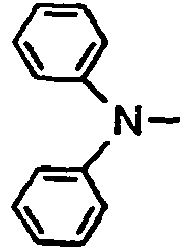
3 H- 
3 H- 163 (II) 
3 H- 
3 H- 164 (II) 
3 H- 
3 H- Table 32 Compound No. General formula R1 Substition position R2 R3 Substition position R4 165 (II) 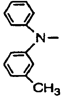
3 H- 
3 H- 166 (II) H- 3 H- 
3 H- 167 (II) H- 3 H- 
3 H- 168 (II) H- 3 H- 
3 H- 169 (II) H- 3 H- 
3 H- Table 33 Compound No. General formula R1 R2 R3 Substition position R4 170 (II) H- H- 
3 H- 171 (II) H- H- 
3 H- 172 (II) H- H- 3 H- 173 (II) H- H- 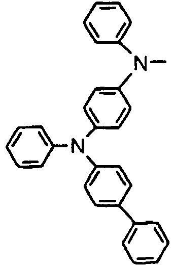
3 H- 174 (II) H- H- 
3 H- Table 34 Compound No. General formula R1 R2 R3 Substition position R4 175 (II) H- H- 
3 H- 176 (II) H- H- 
3 H- 177 (II) H- H- 
3 H- 178 (II) H- H- 
3 H- 179 (II) H- H- 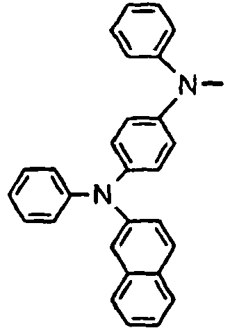
3 H- Table 35 Compound No. General formula R1 R2 R3 Substition position R4 180 (II) H- H- 
3 H- 181 (II) H- H- 
3 H- 182 (II) H- H- 
3 H- 183 (II) H- H- 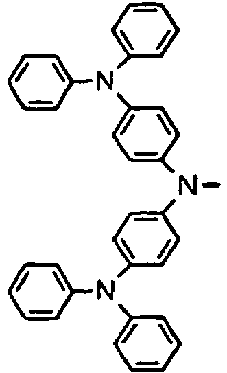
3 H- Table 36 Compound No. General formula R1 R2 R3 Substition position R4 184 (II) H- H- 
3 H- 185 (II) H- H- 
3 H- 186 (II) H- H- 
3 H- 187 (II) H- H- 
3 H- Table 37 Compound No. General formula R1 R2 R3 Substition position R4 188 (II) H- H- 
3 H- 189 (II) H- H- 
3 H- 190 (II) H- H- 
3 H- Table 38 Compound No. General formula R1 Substition position R2 Substition position R3 R4 191 (II) 
3 
3 H- H- 192 (II) 
3 
3 H- H- 193 (II) 
3 
3 H- H- 194 (II) 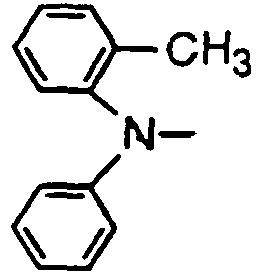
3 
3 H- H- 195 (II) 
3 
3 H- H- 196 (II) 
3 
3 H- H- Table 39 Compound No. General formula R1 Substition position R2 Substition position R3 R4 197 (II) 
3 
3 H- H- 198 (II) 
3 
3 H- H- 199 (II) 
3 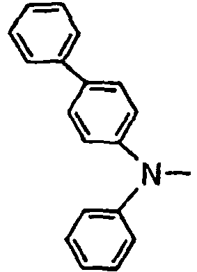
3 H- H- 200 (II) 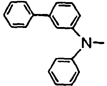
3 
3 H- H- 201 (II) 
3 
3 H- H- 202 (II) 
3 
3 H- H- Table 40 Compound No. General formula R1 Substition position R2 Substition position R3 R4 203 (II) 
3 
3 H- H- 204 (II) 
3 
3 H- H- 205 (II) 
3 
3 H- H- 206 (II) 
3 
3 H- H- 207 (II) 
3 
3 H- H- Table 41 Compound No. General formula R1 Substition position R2 Substition position R3 R4 208 (II) 
3 
3 H- H- 209 (II) 
3 
3 H- H- 210 (II) 
3 
3 H- H- 211 (II) 
3 
3 H- H- Table 42 Compound No. General formula R1 Substition position R2 Substition position R3 R4 212 (II) 
3 
3 H- H- 213 (II) 
3 
3 H- H- 214 (II) 
3 
3 H- H- 215 (II) 
3 
3 H- H- 216 (II) 
3 
3 H- H- Table 43 Compound No. General formula R1 Substition position R2 Substition position R3 Substition position R4 217 (II) 
3 
3 H- 3 H- 218 (II) 
3 
3 
3 H- 219 (II) 
3 
3 
3 H- 220 (II) 
3 
3 
3 H- 221 (II) 
3 
3 
3 H 222 (II) 
3 
3 
3 H- Table 44 Compound No. General formula R1 Substition position R2 Substition position R3 Substition position R4 Substition position 223 (II) 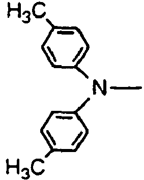
3 
3 
3 H- 3 224 (II) 
3 
3 
3 H- 3 225 (II) 
3 
3 
3 H- 3 226 (II) 
3 
3 
3 
3 227 (II) 
3 
3 
3 
3 228 (II) 
3 
3 
3 
3 Table 45 Compound No. General formula R1 Substition position R2 Substition position R3 Substition position R4 Substition position 229 (II) 
3 
3 
3 
3 230 (II) 
3 
3 
3 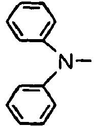
3 231 (II) 
3 
3 
3 
3 232 (II) 
3 
3 
3 
3 233 (II) 
3 
3 
3 
3 Table 46 Compound No. General formula R1 Substition position R2 R3 Substition position R4 234 (II) 
3 H- 
3 H- 235 (II) 
3 H- 
3 H- 236 (II) 
3 H- 
3 H- 237 (II) 
3 H- 
3 H- 238 (II) 
3 H- 
3 H- Table 47 Compound No. General formula R1 Substition position R2 R3 Substition position R4 239 (II) 
3 H- 
4 H- 240 (II) 
3 H- 
4 H- 241 (II) 
3 H- 
4 H- 242 (II) 
3 H- 
4 H- 243 (II) 
3 H- 
4 H- 244 (II) 
3 H- 
4 H- 245 (II) 
3 H- 
4 H- 246 (II) 
3 H- 
4 H- Table 48 Compound No. General formula R1 Substition position R2 R3 Substition position R4 247 (II) 
3 H- 
4 H- 248 (II) 
3 H- 
4 H- 249 (II) 
3 H- 
4 H- 250 (II) 
3 H- 
4 H- 251 (II) 
3 H- 
4 H- 252 (II) 
3 H- 
4 H- Table 49 Compound No. General formula R1 Substition position R2 R3 Substition position R4 253 (II) 
3 H- 
4 H- 254 (II) 
3 H- 
4 H- 255 (II) 
3 H- 
4 H- 256 (II) 
3 H- 
4 H- 257 (II) 
3 H- 
4 H- Table 50 Compound No. General formula R1 Substition position R2 Substition position R3 R4 258 (II) 
3 
4 H- H- 259 (II) 
3 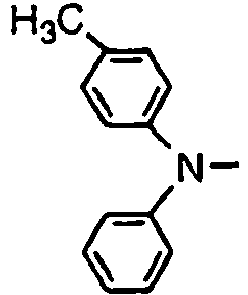
4 H- H- 260 (II) 
3 
4 H- H- 261 (II) 
3 
4 H- H- 262 (II) 
3 
4 H- H- 263 (II) 
3 
4 H- H- 264 (II) 
3 
4 H- H- 265 (II) 
3 
4 H- H- Table 51 Compound No. General formula R1 Substition position R2 Substition position R3 Substition position R4 266 (II) 
3 
3 
4 H- 267 (II) 
3 
4 
4 H- 268 (II) 
4 
3 
4 H- 269 (II) 
4 
4 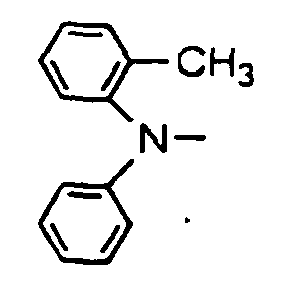
3 H- 270 (II) 
4 
3 
4 H- 271 (II) 
3 
4 
3 H- 272 (II) 
4 
3 
4 H- 273 (II) 
4 
4 
3 H- Table 52 Compound No. General formula R1 Substition position R2 Substition position R3 Substition position R4 Substition position 274 (II) 
3 
3 
4 
4 275 (II) 
3 
4 
3 
4 276 (II) 
3 
4 
3 
4 277 (II) 
4 
4 
4 
3 278 (II) 
3 
4 
3 
4 279 (II) 
4 
4 
3 
3 280 (II) 
4 
3 
4 
3 281 (II) 
4 
4 
4 
3 Table 53 Compound No. General formula R1 Substition position R2 R3 Substition position R4 282 (II) 
4 H- 
4 H- 283 (II) 
4 H- 
4 H- 284 (II) 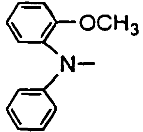
4 H- 
4 H- 285 (II) 
4 H- 
4 H- 286 (II) 
4 H- 
4 H- 287 (II) 
4 H- 
4 H- 288 (II) 
4 H- 
4 H- Table 54 Compound No. General formula R1 Substition position R2 R3 Substition position R4 289 (II) 
4 H- 
4 H- 290 (II) 
4 H- 
4 H- 291 (II) 
4 H- 
4 H- 292 (II) 
4 H- 
4 H- 293 (II) 
4 H- 
4 H- 294 (II) 
4 H- 
4 H- Table 55 Compound No. General formula R1 Substition position R2 Substition position R3 Substition position R4 Substition position 295 (II) 
4 
4 
4 
4 296 (II) 
4 
3 
4 
3 297 (II) 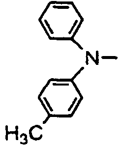
4 
2,3 
4 
2,3 298 (II) 
4 
3,4 
4 
3,4 299 (II) 
4 
4 
4 
4 300 (II) 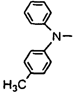
4 
4 
4 
4 Table 56 Compound No. General formula R1 Substition position R2 R3 Substition position R4 301 (III) 
4 H- 
4 H- 302 (III) 
4 H- 
4 H- 303 (III) 
4 H- 
4 H- 304 (III) 
4 H- 
4 H- 305 (III) 
3 H- 
3 H- 306 (III) 
3 H- 
3 H- 307 (III) 
4 H- 
3 H- Table 57 Compound No. General formula R1 Substition position R2 R3 Substition position R4 308 (III) 
4 H- 
4 H- 309 (III) 
4 H- 
4 H- 310 (III) 
3 H- 
3 H- 311 (III) 
4 H- 
3 H- 312 (III) 
4 H- 
4 H- 313 (III) 
3 H- 
3 H- 314 (III) 4 H- 
3 H- Table 58 Compound No. General formula R1 Substition position R2 R3 Substition position R4 315 (III) 
4 H- 
4 H- 316 (III) 4 H- 4 H- 317 (III) 3 H- 3 H- 318 (III) 
3 H- 
3 H- 319 (III) 4 H- 3 H- 320 (III) 
4 H- 
4 H- Table 59 Compound No. General R1 formula Substition position R2 Substition position R3 Substition position R4 Substition position 321 (III) H- H- 
4 H- 322 (III) H- H- 
3 H- 323 (III) 
4 
4 H- H- H- 324 (III) 
4 
4 
4 H- 325 (III) 
4 
4 
4 
4 Table 60 Compound No. General formula R1 Substition position R2 R3 Substition position R4 326 (IV) 
4 H- 
4 H- 327 (IV) 
4 H- 
4 H- 328 (IV) 
4 H- 
4 H- 329 (IV) 
4 H- 
4 H- 330 (IV) 
3 H- 
3 H- 331 (IV) 
3 H- 
3 H- 332 (IV) 
3 H- 
3 H- Table 61 Compound No. General formula R1 Substition position R2 R3 Substition position R4 333 (IV) 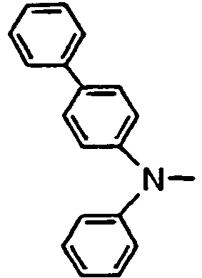
4 H- 
4 H- 334 (IV) 
4 H- 
4 H- 335 (IV) 
3 H- 
3 H- 336 (IV) 
4 H- 
3 H- 337 (IV) 
4 H- 
4 H- 338 (IV) 
3 H- 
3 H- 339 (IV) 
4 H- 
3 H- Table 62 Compound No. General formula R1 Substition position R2 R3 Substition position R4 340 (IV) 
4 H- 
4 H- 341 (IV) 
4 H- 
4 H- 342 (IV) 
3 H- 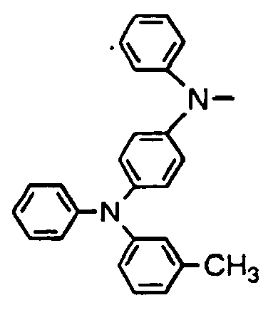
3 H- 343 (IV) 
3 H- 
3 H- 344 (IV) 
4 H- 
3 H- 345 (III) 
4 H- 
4 H- 
Table 64 Compound No. General formula R1 Substition position R2 R3 Substition position R4 351 (V) 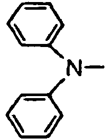
4 H- 
4 H- 352 (V) 
4 H- 
4 H- 353 (V) 
4 H- 
4 H- 354 (V) 
4 H- 
4 H- 355 (V) 
4 H- 
4 H- 356 (V) 
4 H- 
4 H- 357 (V) 
4 H- 
4 H- Table 65 Compound No. General formula R1 Substition position R2 R3 Substition position R4 358 (V) 
4 H- 
4 H- 359 (V) 
4 H- 
4 H- 360 (V) 
4 H- 
4 H- 361 (V) 
4 H- 
4 H- 362 (V) 
4 H- 
4 H- 363 (V) 
4 H- 
4 H- 364 (V) 
4 H- 
4 H- Table 66 Compound No. General formula R1 Substition position R2 R3 Substition position R4 365 (V) 
4 H- 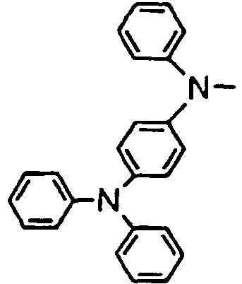
4 H- 366 (V) 
4 H- 
4 H- 367 (V) 
4 H- 
4 H- 368 (V) 
4 H- 
4 H- Table 67 Compound No. General formula R1 Substition position R2 R3 Substition position R4 369 (V) 
3 H- 
3 H- 370 (V) 
3 H- 
3 H- 371 (V) 
3 H- 
3 H- 372 (V) 
3 H- 
3 H- 373 (V) 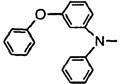
3 H- 
3 H- 374 (V) 
3 H- 
3 H- 375 (V) 
3 H- 
4 H- Table 68 Compound No. General formula R1 Substition position R2 R3 Substition position R4 376 (V) 
3 H- 
3 H- 377 (V) 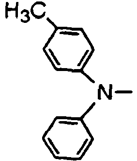
3 H- 
3 H- 378 (V) 
3 H- 
3 H- 379 (V) 
3 H- 
3 H- 380 (V) 
3 H- 
3 H- 381 (V) 
3 H- 
3 H- 382 (V) 
3 H- 
3 H- Table 69 Compound No. General formula R1 Substition position R2 R3 Substition position R4 383 (V) 
3 H- 
3 H- 384 (V) 
3 H- 
3 H- 385 (V) 
3 H- 
3 H- 386 (V) 
3 H- 
3 H- Table 70 Compound No. General formula R1 Substition position R2 R3 Substition position R4 387 (VI) 
4 H- 
4 H- 388 (VI) 
4 H- 
4 H- 389 (VI) 
4 H- 
4 H- 390 (VI) 
4 H- 
4 H- 391 (VI) 
4 H- 
4 H- 392 (VI) 
4 H- 
4 H- 393 (VI) 
4 H- 
4 H- Table 71 Compound No. General formula R1 Substition position R2 R3 Substition position R4 394 (VI) 
4 H- 
4 H- 395 (VI) 
4 H- 
4 H- 396 (VI) 
4 H- 
4 H- 397 (VI) 
4 H- 
4 H- 398 (VI) 
4 H- 
4 H- 399 (VI) 
4 H- 
4 H- 400 (VI) 
4 H- 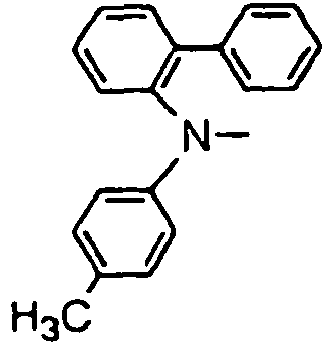
4 H- Table 72 Compound No. General formula R1 Substition position R2 R3 Substition position R4 401 (VI) 
4 H- 
4 H- 402 (VI) 
4 H- 
4 H- 403 (VI) 
4 H- 
4 H- 404 (VI) 
4 H- 
4 H- Table 73 Compound No. General formula R1 Substition position R2 R3 Substition position R4 405 (VI) 
3 H- 
3 H- 406 (VI) 3 H- 
3 H- 407 (VI) 
3 H- 
3 H- 408 (VI) 
3 H- 
3 H- 409 (VI) 
3 H- 
3 H- 410 (VI) 
3 H- 
3 H- 411 (VI) 
3 H- 
4 H- Table 74 Compound No. General formula R1 Substition position R2 R3 Substition position R4 412 (VI) 
3 H- 
3 H- 413 (VI) 
3 H- 
3 H- 414 (VI) 
3 H- 
3 H- 415 (VI) 
4 H- 
3 H- 416 (VI) 
3 H- 
3 H- 417 (VI) 
4 H- 
3 H- 418 (VI) 
3 H- 
3 H- Table 75 Compound No. General formula R1 Substition position R2 R3 Substition position R4 419 (VI) 
3 H- 
3 H- 420 (VI) 
3 H- 
3 H- 421 (VI) 
3 H- 
3 H- 422 (VI) 
3 H- 
3 H- Table 76 Compound No. General formula R1 Substition position R2 R3 Substition position R4 R5 423 (VII) 
4 H- 
4 H- 
424 (VII) 
4 H- 
4 H- 
425 (VII) 
4 H- 
4 H- 
426 (VII) 
4 H- 
4 H- 
427 (VII) 
4 H- 
4 H- 
428 (VII) 
4 H- 
4 H- 
Table 77 Compound No. General formula R1 Substition position R2 R3 Substition position R4 R5 429 (VII) 
4 H- 
4 H- 
430 (VII) 
4 H- 
4 H- 
431 (VII) 
4 H- 
4 H- 
432 (VII) 
4 H- 
4 H- 
433 (VII) 
4 H- 
4 H- 
434 (VII) 
4 H- 
4 H- 
435 (VII) 
4 H- 
4 H- 
436 (VII) 
4 H- 
4 H- 
Table 78 Compound General No. formula R1 Substition position R2 R3 Substition position R4 R5 437 (VII) 
4 H- 
4 H- 
438 (VII) 
4 H- 
4 H- 
439 (VII) 
4 H- 
4 H- 
440 (VII) 
4 H- 
4 H- 
441 (VII) 
4 H- 
4 H- 
442 (VII) 
4 H- 
4 H- 
- The compounds of the invention may have such structures as given below.


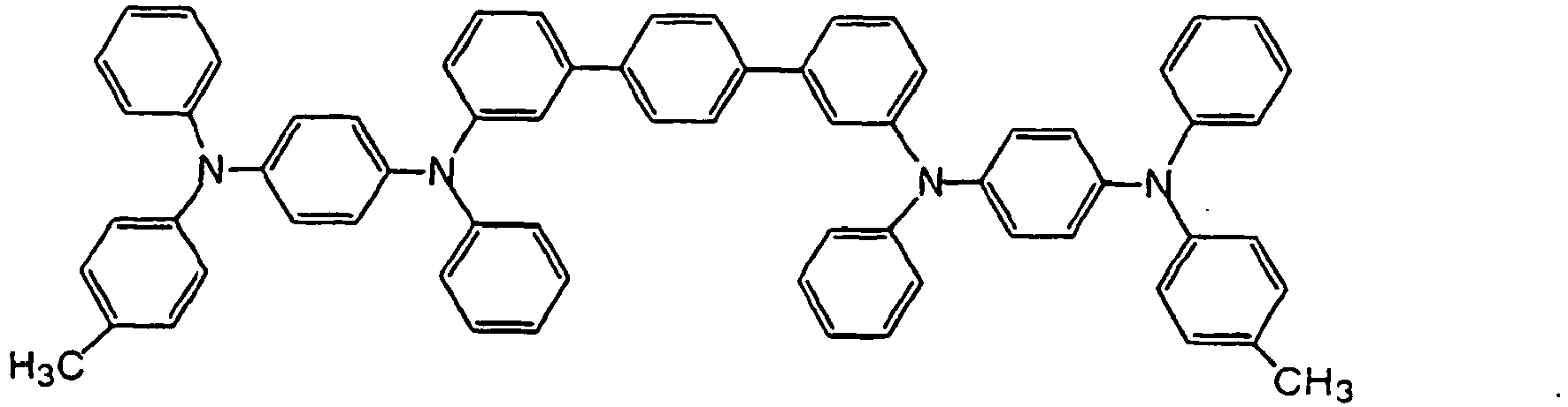


- The compounds of the invention may be synthesized by the Ullmann reaction for the condensation of, for instance, a primary or secondary aromatic amine and an aromatic iodide using a catalyst such as copper. When R01 and R02 are asymmetric with respect to R03 and R04 (both sides of the biphenyl moieties are asymmetric), R01 and R02, and R03 and R04 may synthesize the corresponding amines, finally followed by the coupling of the biphenyl moieties (guanine coupling, Ni(dppp)Cl2, etc.).
- Illustrative synthesis examples are given below as (1) to (4). Using copper as the catalyst, 4,4'-diiodobiphenyl is coupled to a compound having formula (A) in (1), and a compound,having formula (B) is coupled to a compound having formula (C) in (2), thereby obtaining an asymmetric compound having formula (D). In (3), a compound having formula (E) is coupled to a compound having formula (F) using Ni(dppp)Cl2 to obtain an asymmetric compound having formula (G). In (4), an asymmetric compound having formula (K) is synthesized from a compound having formula (J), and a compound having formula (I) obtained from a compound having formula (H). Here it is to be noted that R30, R41, R45 and R50 in the following formulae (A) to (K) are tantamount to R01, R02, R03 and R04 in general formula (I), respectively, and R32, R33, R42, R43, R45, R47, R52 and R53 are tantamount to R11, R12, R13, R14, R15, R16 and R17 in general formula (I), respectively.


- The compounds of the invention may be identified by mass spectroscopy, infrared absorption spectra (IR), 1H or 13C nuclear magnetic resonance spectra (NMR) or the like.
- These compounds of the invention have a molecular weight of the order of 640 to 2,000 and a high melting point of 190 to 300°C, and show a high glass transition temperature of 80 to 200°C. They are put as by ordinary vacuum evaporation into a transparent amorphous state which is stable even at higher than room temperature; that is, they are obtained in the form of a smooth and good film which is maintained intact over an extended period. It is here to be noted that some of the compounds of the invention have no melting point and exist in an amorphous state even at high temperatures. It is thus possible to obtain a homogeneous thin film that is by itself stable without recourse to a binder resin.
- By using the compounds of the invention, the Hole mobility is so improved that a device having an increased current density can be obtained. The Hole mobility obtained by the compound of the invention is preferably at least 1.0 × 10⁻³ cm2/Vs, especially 1.1 x 10⁻³ to 100 x 10-3 cm2/Vs, and more especially 1.1 x 10⁻³ to 20.0 x 10⁻³ cm2/Vs. The Hole mobility of the layer containing the compound of the invention is preferably up to 1/2, especially about 1/4 to 1/1,000, and more especially about 1/4 to 1/100 of that of the light emitting layer. In the invention, the hole injecting layer is formed of the compound of the invention which imparts such excellent Hole mobility thereto. Even when such a hole injecting layer has a thickness of at least 100 nm, and especially at least 200 nm, there is obtained a device that can be operated with no difficulty. It is here to be noted that the upper limit on the thickness of the hole injecting layer is usually about 5,000 nm although the invention is not limited thereto. In the practice of the invention, this film thickness may be determined in such a manner that, while the optical refractive index of each layer is taken into account, the optimum light extraction efficiency is obtained with no problem in conjunction with the angle of view, etc.
- The compounds according to the invention may be used alone or in combination of two or more.
- The EL device of the invention comprises at least one organic compound layer, and said at least one organic compound layer comprises the compound or compounds of the invention. One exemplary construction of the organic EL device according to the invention is shown in
Fig. 1 . As illustrated, the organic EL device comprises ahole injecting electrode 3, a hole injecting and transportinglayer 4, alight emitting layer 5, an electron injecting and transportinglayer 6 and anelectron injecting electrode 7 in the described order. Furthermore, if acolor filter 8, afluorescence conversion filter 9, an organic EL device as mentioned above, asealing layer 10 and acover 11 are stacked and formed on aglass substrate 2 in the described order, an organic EL color display is then obtained. - The light emitting layer has functions of injecting holes and electrons, transporting them, and recombining holes and electrons to create excitons. The hole injecting and transporting layer has functions of facilitating injection of holes from the hole injecting electrode, providing stable transportation of holes and blocking electrons, and the electron injecting and transporting layer has functions of facilitating injection of electrons from the electron injecting electrode, providing stable transportation of electrons and blocking holes. These layers are effective for increasing the number of holes and electrons injected into the light emitting layer and confining holes and electrons therein for optimizing the recombination region to improve light emission efficiency. The electron injecting and transporting layer and the hole injecting and transporting layer may be provided, if required, while care is taken of the magnitudes of the functions which the compound used for the light emitting layer has in injecting electrons, transporting electrons, injecting holes, and transporting holes. For instance, when the compound used for the light emitting layer has great functions in injecting and transporting holes or electrons, the hole or electron injecting and transporting layer may be dispensed with; that is, the light emitting layer may be allowed to function as a hole injecting and transporting layer or an electron injecting and transporting layer. In some cases, both the hole injecting and transporting layer and the electron injecting and transporting layer may be dispensed with. Alternatively, the hole injecting and transporting layer and the electron injecting and transporting layer may be each separated into an injecting layer and a transporting layer.
- By controlling the thickness of the organic layer while care is taken of the carrier mobility or carrier density (determined depending on ionization potential and electron affinity) of the light emitting layer, electron injecting and transporting layer or hole injecting and transporting layer to be combined therewith, it is possible to freely determine the recombination/light emitting region. It is in turn possible to design the color of light to be emitted, and control emission luminance and spectra due to the interference effect between both electrode as well as the spatial distribution of light emission.
- The compound of the invention may be applied to any one of the hole injecting layer, hole transporting layer, light emitting layer, and hole injecting and transporting layer. Since the compound of the invention is excellent in the capability of injecting holes, however, it is preferably applied to the hole injecting layer or hole injecting and transporting layer, especially the hole injecting layer. With the compound of the invention that has both the phenylenediamine skeleton and the diamine skeleton including a plurality of phenylene radicals such as a benzidine skeleton, it is possible to freely control ionization potential and carrier mobility without sacrifice of heat resistance and, hence, optimize hole injection efficiency depending on the material to be combined therewith.
- Here an account is given of the case where the compound of the invention is used for the hole injecting and transporting layer. The hole injecting and transporting layer may be formed by the evaporation of the compound of the invention or the coating of a dispersion of the compound of the invention in a resin binder. Especially the evaporation of the compound of the invention yields a good enough amorphous film.
- When the compound of the invention is used for the hole injecting and transporting layer, the fluorescent material used for the light emitting layer may be selected from materials emitting fluorescence of longer wavelength. For instance, a sensible selection may be made from at least one fluorescent material used for the light emitting layer in combination with the compound of the invention. In such a case, too, the compound of the invention may be applied to the light emitting layer.
- In this case, the compound of the invention may be used. However, the compound of the invention has the phenylenediamine skeleton contributing to very strong donicity, and so is susceptible to interaction with the light emitting layer, resulting a drop of the intensity of fluorescence due to the formation of exciplexes, etc. This in turn offers problems such as a light emission efficiency drop, and a color purity drop due to the broadening of emission spectra, and so is undesired. When a light emitting material having no interaction with the compound of the invention, however, the compound of the invention may be used as a hole transporting material.
- The hole injecting and transporting layer may be formed of a combination of more than one of hole injecting and transporting materials. In a particularly preferred embodiment, hole injecting and transporting materials are laminated on ITO in the order of increasing ionization potential, for instance, in the order of a hole injecting layer and a hole transporting layer. Thus, it is preferable to form on the ITO surface a hole injecting material having a good thin film property so that a uniform thin film can be formed on the ITO surface having a varying hydrophilic nature. Since evaporation is utilized in the manufacture of devices, films as thin as about 1 to 10 nm can be formed in a uniform and pinhole-free state. If film thickness, refractive index, etc. are regulated, it is then possible to prevent an efficiency drop by controlling the color of light emitted and emission luminance or making use of interference light effects such as the spatial distribution of light emission.
- For the hole transporting layer opposite to the light emitting layer, it is preferable to use a triarylamine polymer having a benzidine skeleton alone and less susceptible to interaction with the light emitting material, such as those set forth in
JP-A's 63-295695 5-234681 7-43564 - In the invention, the light emitting layer may contain a fluorescent material. The fluorescent material used herein, for instance, may be at least one compound selected from compounds such as those disclosed in
JP-A 63-264692 6-110569 6-114456 - Preferably, the fluorescent compound is used in combination with a host substance capable of emitting light by itself; that is, it is preferable that the fluorescent compound is used as a dopant. In such a case, the content of the fluorescent compound in the light emitting layer is in the range of preferably 0.01 to 10% by weight, and especially 0.1 to 5% by weight. By using the fluorescent compound in combination with the host substance, it is possible to vary the wavelength performance of light emission, thereby making light emission possible on a longer wavelength side and, hence, improving the light emission efficiency and stability of the device.
- Quinolinolato complexes, and aluminum complexes containing 8-quinolinol or its derivatives as ligands are preferred for the host substance. Such aluminum complexes are typically disclosed in
JP-A's 63-264692 3-255190 5-70733 5-258859 6-215874 - Exemplary aluminum complexes include tris(8-quinolinolato)aluminum, bis(8-quinolinolato)magnesium, bis(benzo{f}-8-quinolinolato)zinc, bis(2-methyl-8-quinolinolato)aluminum oxide, tris(8-quinolinolato)indium, tris(5-methyl-8-quinolinolato)aluminum, 8-quinolinolato-lithium, tris(5-chloro-8-quinolinolato)gallium, bis(5-chloro-8-quinolinolato)calcium, 5,7-dichloro-8-quinolinolatoaluminum, tris(5,7-dibromo-8-hydroxyquinolinolato)aluminum, and poly[zinc(II)-bis(8-hydroxy-5-quinolinyl)methane].
- Use may also be made of aluminum complexes containing other ligands in addition to 8-quinolinol or its derivatives, for instance, bis(2-methyl-8-quinolinolato)(phenolato) aluminum (III), bis(2-methyl-8-quinolinolato)(o-cresolato) aluminum (III), bis(2-methyl-8-quinolinolato)(m-cresolato) aluminum (III), bis(2-methyl-8-quinolinolato)(p-cresolato) aluminum (III), bis(2-methyl-8-quinolinolato)(o-phenylphenolato)aluminum (III), bis(2-methyl-8-quinolinolato) (m-phenylphenolato)aluminum (III), bis(2-methyl-8-quinolinolato) (p-phenylphenolato)aluminum (III), bis (2-methyl-8-quinolinolato)(2,3-dimethylphenolato)aluminum (III), bis(2-methyl-8-quinolinolato)(2,6-dimethylphenolato)aluminum (III), bis (2-methyl-8-quinolinolato) (3,4-dimethylphenolato)aluminum (III), bis(2-methyl-8-quinolinolato)(3,5-dimethylphenolato) aluminum (III), bis(2-methyl-8-quinolinolato)(3,5-di-tert-butylphenolato)aluminum (III), bis(2-methyl-8-quinolinolato)(2,6-diphenylphenolato)aluminum (III), bis(2-methyl-8-quinolinolato) (2,4,6-triphenylphenolato)aluminum (III), bis(2-methyl-8-quinolinolato)(2,3,6-trimethylphenolato)aluminum (III), bis(2-methyl-8-quinolinolato) (2,3,5,6-tetramethylphenolato)aluminum (III), bis(2-methyl-8-quinolinolato)(1-naphtholato)aluminum (III), bis(2-methyl-8-quinolinolato)(2-naphtholato)aluminum (III), bis(2,4-dimethyl-8-quinolinolato)(o-phenylphenolato)aluminum (III), bis(2,4-dimethyl-8-quinolinolato) (p-phenylphenolato)aluminum (III), bis(2,4-dimethyl-8-quinolinolato) (m-phenylphenolato) aluminum (III), bis(2,4-dimethyl-8-quinolinolato)(3,5-dimethylphenolato)aluminum (III), bis(2,4-dimethyl-8-quinolinolato)(3,5-di-tert-butylphenolato)aluminum (III), bis(2-methyl-4-ethyl-8-quinolinolato)(p-cresolato)aluminum (III), bis(2-methyl-4-methoxy-8-quinolinolato)(p-phenylphenolato)aluminum (III), bis(2-methyl-5-cyano-8-quinolinolato)(o-cresolato)aluminum (III), and bis(2-methyl-6-trifluoromethyl-8-quinolinolato)(2-naphtholato)aluminum (III).
- Besides, use may be made of bis(2-methyl-8-quinolinolato)aluminum (III)-µ-oxo-bis(2-methyl-8-quinolinolato) aluminum (III), bis(2,4-dimethyl-8-quinolinolato)aluminu_m (III)-µ-oxo-bis(2,4-dimethyl-8-quinolinolato)aluminum (III), bis(4-ethyl-2-methyl-8-quinolinolato)aluminum (III)-µ-oxo-bis(4-ethyl-2-methyl-8-quinolinolato)aluminum (III), bis(2-methyl-4-methoxyquinolinolato)aluminum (III)-µ-oxo-bis(2-methyl-4-methoxyquinolinolato)aluminum (III), bis(5-cyano-2-methyl-8-quinolinolato)aluminum (III)-µ-oxo-bis(5-cyano-2-methyl-8-quinolinolato)aluminum (III), bis(2-methyl-5-trifluoromethyl-8-quinolinolato)aluminum (III)-µ-oxo-bis(2-methyl-5-trifluoromethyl-8-quinolinolato)aluminum (III), ecc.
- Other preferable host substances include phenylanthracene derivatives disclosed in Japanese Patent Application No.
6-110569 6-114456 - The phenylanthracene derivatives are represented by the following formula (VIII):
A1-L1-A2 (VIII)
- In formula (VIII), A1 and A2 may be identical with or different from each other, and are each a monophenylanthryl or diphenylanthryl group.
- The monophenylanthryl or diphenylanthryl group represented by A1, and A2 may, or may not, have a substituent. The substituent, for instance, may be an alkyl, aryl, alkoxy, aryloxy or amino group which may have another substituent. Where is substituted by such a substituent is not critical in the invention. However, it is preferable that the phenyl group attached to the anthracene ring rather than the anthracene ring per se is substituted by such a substituent. Preferably in this case, the bond position of the phenyl group in the anthracene ring is the 9- or 10-position in the anthracene ring.
- In formula (VIII), L1 stands for a single bond or an arylene group. The arylene group given by L1 is preferably unsubstituted. For instance, the arylene group includes an ordinary arylene group such as a phenylene group, a biphenylene group, and an anthrylene group as well as two or more such arylene groups attached directly to each other. L1 is preferably a single bond, and a p-phenylene or 4,4'-biphenylene group.
- L1 may also include two or more such arylene groups as attached to each other via an alkylene group, -O-, -S- or - NR- where R is an alkyl or aryl group. For instance, a methyl or ethyl group is mentioned for the alkyl group and a phenyl group is mentioned for the aryl group. Particular preference is given to the aryl group, for instance, a phenyl group as well as A1 and A2. A phenyl group with A1 or A2 attached thereto may also be acceptable. Preferred for the alkylene group are a methylene group, an ethylene group or the like. Examples of such an arylene group are given below.
- The tetraarylethene derivatives are represented by the following formula (IX):

- In formula (IX), Ar1, Ar2 and Ar3 may be identical with or different from one another, and are each an aromatic residue.
- Aromatic hydrocarbon groups (aryl groups), and aromatic heterocyclic groups, for instance, may be mentioned for the aromatic residues represented by Ar1, Ar2 and Ar3. The aromatic hydrocarbon groups may monocyclic or polycyclic aromatic hydrocarbon groups, and include fused rings or ring combinations as well. Each aromatic hydrocarbon group has preferably 6 to 30 carbon atoms in all, and may have a substituent represented by an alkyl group, an aryl group, an alkoxy group, an aryloxy group, an amino group or the like. The aromatic hydrocarbon groups, for instance, include phenyl, alkylphenyl, alkoxyphenyl, arylphenyl, aryloxyphenyl, aminophenyl, biphenyl, naphthyl, anthryl, pyrenyl, and perylenyl groups.
- The aromatic heterocyclic groups are preferably those containing O, N, and S as a hetero-atom, and may each be a five- or six-membered ring. For instance, thienyl, furyl, pyrrolyl and pyridyl groups are mentioned.
- A phenyl group is particularly preferred for the aromatic group represented by Ar1, Ar2, and Ar3.
- The letter n is an integer of preferably 2 to 6, and especially 2 to 4.
- L2 is an n-valent aromatic residue. It is preferably a di- to hexa-valent, especially di- to tetra-valent residue derived from an aromatic hydrocarbon, an aromatic heterocyclic ring, an aromatic ether or an aromatic amine. This aromatic residue, which may have a substituent, is preferably unsubstituted.
- The light emitting layer is formed by using the compound of formula (IX) in combination with the aforesaid host material. It is also preferred that the light emitting layer is formed of a mixed layer of at least one compound capable of injecting and transporting holes with at least one compound capable of injecting and transporting electrons. Preferably in this case, a dopant is incorporated in the mixed layer. The content of the dopant compound in the mixed layer is in the range of preferably 0.01 to 20% by weight, and especially 0.1 to 15% by weight.
- In the mixed layer with a hopping conduction path available for carriers, each carrier migrates in the polarly prevailing substance, so making the injection of carriers having an opposite polarity unlikely to occur. This leads to an increase in the service life of the device due to less damage to the organic compound. By incorporating the compound of formula (IX) in such a mixed layer, it is possible to vary the wavelength performance of light emission that the mixed layer itself possesses, thereby shifting the wavelength of light emission to a longer wavelength side and improving the intensity of light emission, and the stability of the device as well.
- The compound capable of injecting and transporting holes and the compound capable of injecting and transporting electrons, both used to form the mixed layer, may be selected from compounds for the injection and transportation of holes and compounds for the injection and transportation of electrons. Especially for the compounds capable of injecting and transporting electrons, it is preferable to use metal complexes containing quinoline derivatives, especially 8-quinolinol or its derivatives as ligands, in particular, tris(8-quinolinolato) aluminum (Alq3). It is also preferable to use the aforesaid phenylanthracene derivatives, and tetraarylamine derivatives.
- For the compounds for the injection and transportation of holes, it is preferable to use amine derivatives having strong fluorescence, for instance, hole transporting materials such as tetraphenyldiamine derivatives, styrylamine derivatives, and amine derivatives having an aromatic fused ring, as already mentioned.
- In this case, the mixing ratio is determined while the carrier mobility and carrier density are taken into consideration. In general, however, it is preferred that the weight ratio between the compound capable of injecting and transporting holes and the compound capable of injecting and transporting electrons is of the order of 1/99 to 99/1, particularly 10/90 to 90/10, and more particularly 20/80 to 80/20.
- The thickness of the mixed layer must correspond to che thickness of a single molecular layer, and so is preferably less than the thickness of the organic compound layer. More specifically, the mixed layer has a thickness of preferably 1 to 85 nm, especially 5 to 60 nm, and more especially 5
co 50 nm. - Preferably, the mixed layer is formed by co-evaporation where the selected compounds are evaporated from different evaporation sources. When the compounds to be mixed have identical or slightly different vapor pressures (evaporation temperatures), however, they may have previously been mixed together in the same evaporation boat for the subsequent evaporation. Preferably, the compounds are uniformly mixed together in the mixed layer. However, the compounds in an archipelagic form may be present in the mixed layer. The light emitting layer may generally be formed at a given thickness by the evaporation of the organic fluorescent substance or coating a dispersion of the organic fluorescent substance in a resin binder.
- In the practice of the invention, the electron injecting and transporting layer may be provided. For the electron injecting and transporting layer, there may be used quinoline derivatives such as organic metal complexes containing 8-quinolinol or its derivatives as ligands, for instance, tris(8-quinolinolato)aluminum (Alq3), oxadiazole derivatives, perylene derivatives, pyridine derivatives, pyrimidine derivatives, quinoxaline derivative, diphenylquinone derivatives, and nitro-substituted fluorene derivatives. The electron injecting and transporting layer may also serve as a light emitting layer. In this case, it is preferable to use tris(8-quinolilato)aluminum, etc. Like the light emitting layer, the electron injecting and transporting layer may then be formed by evaporation or the like.
- When the compound of the invention is used for the light emitting layer, the hole, and electron injecting and transporting layer may be formed of various organic compounds as disclosed in
JP-A's 63-295695 2-191694 3-792 - When the compound of the invention is used for the light emitting layer, it is preferable to combine the compound of the invention with the aforesaid light emitting material unlikely to extinguish light due to their interaction. The compound of the invention emits strong blue fluorescence, and so can achieve a high-luminance light emitting device when combined with a material having little interaction therewith.
- The thickness of the light emitting layer, the hole injecting and transporting layer, and the electron injecting and transporting layer is not critical and varies with the design of recombination/light emitting region and a particular formation technique although it is usually of the order of preferably 5 to 500 nm, and especially 10 to 200 nm.
- The thickness of the hole injecting and transporting layers, and the electron injecting and transporting layer is equal to, or about 1/10 times to about 10 times as large as, the thickness of the light emitting layer although it depends on the design of the recombination/light emitting region.
- When the electron or hole injecting and transporting layer is separated into an injecting layer and a transporting layer, it is preferable that the injecting layer is at least 1 nm thick and the transporting layer is at least 1 nm and especially at least 20 nm thick.
- The upper limit on thickness is usually about 500 nm and especially about 100 nm for the injecting layer and about 500 nm for the transporting layer. The same film thickness applies when two injecting and transporting layers are provided.
- By controlling the thickness of the organic layer while care is taken of the carrier mobility or carrier density (determined depending on ionization potential and electron affinity) of the light emitting layer, electron injecting and transporting layer or hole injecting and transporting layer to be combined therewith, it is possible to freely determine the recombination/light emitting region. It is in turn possible to design the color of light to be emitted, and control emission luminance and spectra due to the interference effect between both electrode as well as the spatial distribution of light emission.
- For the electron injecting electrode, it is preferable to use a material having a low work function, for instance, Li, Na, K, Mg, Al, Ag or In, an alloy thereof, or an oxide or halide thereof. It is also preferred that the electron injecting electrode be formed of fine crystal grains, especially in an amorphous state. The electron injecting electrode has preferably a thickness of the order of 10 to 1,000 nm.
- Furthermore, it is preferable to evaporate and sputter Al or a fluorine type compound at the final stage of electrode formation, because an improved sealing effect is obtained with an interconnection resistance drop in the case of Al.
- To allow the EL device to emit light at its surface, it is required that at least one of the two electrodes be transparent or semitransparent. Since there is some limitation on the material of which the electron injecting electrode is formed as mentioned above, however, the material and thickness of the hole injecting electrode are preferably determined such that at least 80% of the light emitted transmits through it. For instance, it is preferable to use ITO (tin-doped indium oxide), IZO (zinc-doped indium oxide), SnO2, Ni, Au, Pt, Pd, and polypyrrole for the hole injecting electrode. It is also preferable that the hole injecting electrode has a thickness of the order of 10 to 500 nm. To improve the reliability of the device, it is required that the driving voltage be low. Preferable to this end is an ITO of 10 to 30 Ω/□ (with a thickness of 80 to 300 nm). In the practice of the invention, the thickness and optical constant of the ITO may be designed such that high light extraction efficiency and high color purity are satisfied by the interference effect due to reflection at the ITO interface.
- To a large device such as a display device, an Al interconnection may be applied because the resistance of the ITO increases.
- Preferably but not exclusively, transparent or translucent materials such as glasses, and resins are used for the substrate material because, in the illustrated embodiment, the emitted light is extracted or taken out of the substrate side. The substrate may be colored or otherwise provided with a color filter film, fluorescence conversion film or dielectric reflecting film for controlling the color of light emitted.
- It is here to be noted that when an opaque material is used for the substrate, the order of lamination shown in
Fig. 1 may be reversed. - For the color filter film, a color filter employed with liquid crystal display devices may be used. However, it is preferable to control the properties of the color filter in conformity to the light emitted from the organic EL device, thereby optimizing the efficiency of taking out light emission and color purity.
- By using a color filter capable of cutting off extraneous light of such wavelength as absorbed by an EL device material or the fluorescence conversion layer, it is possible to improve the light resistance of the device and the contrast of what is displayed on the device.
- Instead of the color filter, an optical thin film such as a dielectric multilayer film may be used.
- The fluorescence conversion film absorbs light emitted from an EL device and gives out light from the phosphors contained therein for the color conversion of light emission, and is composed of three components, a binder, a fluorescent material and a light absorbing material.
- In the practice of the invention, it is basically preferable to use a fluorescent material having high fluorescent quantum efficiency, and especially a fluorescent material having strong absorption in an EL light emission wavelength region. Laser dyes are suitable for the practice of the invention. To this end, for instance, it is preferable to use rohodamine compounds, perylene compounds, cyanine compounds, phthalocyanine compounds (including subphthalocyanine compounds, etc.), naphthaloimide compounds, fused cyclic hydrocarbon compounds, fused heterocyclic compounds, styryl compounds, and coumarin compounds.
- For the binder, it is basically preferable to make an appropriate selection from materials that do not extinguish fluorescence. It is particularly preferable to use a material that can be finely patterned by photolithography, printing or the like. It is also preferable to use a material that is not damaged during ITO film formation.
- The light absorbing material is used when light is not fully absorbed by the fluorescent material, and so may be dispensed with, if not required. For the light absorbing material, it is preferable to make a selection from materials that do not extinguish the fluorescence of the fluorescent material.
- In what follows, how to fabricate the EL device of the invention will now be explained.
- To form the hole, and electron injecting electrode, it is preferable to use vapor phase growth processes such as evaporation, and sputtering.
- To form the hole injecting and transporting layer, the light emitting layer, and the electron injecting and transporting layer, it is preferable to use a vacuum evaporation technique which enables a homogeneous thin film to be obtained. According to the vacuum evaporation process, it is possible to obtain homogeneous thin films in an amorphous state or with a crystal grain diameter of at most 0.1 µm. The use of a thin film having a crystal grain diameter exceeding 0.1 µm results in non-uniform light emission. To avoid this, it is required to increase the driving voltage of the device; however, there is a striking drop of hole injection efficiency.
- No particular limitation is imposed on vacuum evaporation conditions. However, an evaporation rate of the order of 0.01 to 1 nm/sec. is preferably applied at a degree of vacuum of up to 10-5 Torr (10-4 Pa). It is also preferable to form the layers continuously in vacuum. If the layers are continuously formed in vacuum, high properties are then obtained because the adsorption of impurities on the interface between the adjacent layers can be avoided. In addition, the driving voltage of the device can be flowered while the growth and occurrence of dark spots are inhibited.
- When the vacuum evaporation process is used to form the layers, each containing a plurality of compounds, it is preferable to carry out co-evaporation while boats charged with the compounds are individually placed under temperature control.
- The EL device of the invention is generally of the DC drive type while it may be of the AC or pulse drive type. The applied voltage is generally of the order of 2 to 20 volts.
- The present invention are explained more specifically with reference to some synthesis examples and examples.
- In a 200 ml reaction vessel 26 grams of N,N-diphenyl-1,4-phenylenediamine and 22 grams of 3-iodotoluene were heated together with 0.3 grams of activated copper powders, 50 grams of potassium carbonate and 50 ml of decalin at an oil bath temperature of 200°C for 24 hours in an Ar atmosphere. After the completion of the reaction, the reaction solution was filtrated with the addition of 100 ml of toluene thereto, thereby removing insolubles. The filtrate was washed with water, and dried over sodium sulfate. Following this, the solvent was removed by distillation from the filtrate, and the residue was purified twice by means of a silica gel column (using a mixed solvent of n-hexane and toluene as a developing solvent), thereby obtaining 17 grams of N,N'-diphenyl-N-(3-tolyl)-1,4-phenylenediamine.
- Then, in a 200
ml reaction vessel 10 grams of N,N'diphenyl-N-(3-tolyl)-1,4-phenylenediamine obtained as mentioned above and 4.6 grams of 4,4'-diiodobiphenyl were heated together with 0.3 grams of activated copper powders, 8.0 grams of potassium carbonate and 100 ml of decalin at an oil bath temperature of 220°C for 40 hours in an Ar atmosphere. After the completion of the reaction, the reaction solution was filtrated with the addition of 200 ml of toluene thereto, thereby removing insolubles. The filtrate was washed with water, and dried over sodium sulfate. Following this, the solvent was removed by distillation from the filtrate, and the residue was purified four times by means of a silica gel column (using a mixed solvent of n-hexane and toluene as a developing solvent), thereby obtaining 7 grams of N,N'-diphenyl-N,N-bis[N-phenyl-N-3-tolyl(4-aminophenyl)] benzidine, 2 grams of which were purified by sublimation to obtain 1.8 grams of a slightly pale yellow glassy compound emitting strong blue fluorescence. This compound has a structure mentioned below as HIM33.
1H-NMR spectra are shown inFig. 2 .
13C-NMR spectra are shown inFig. 3 .
Infrared absorption spectra are shown inFig. 4 .
Differential scanning calorimetry (DSC)
Melting point: 234°C (partially amorphous)
Glass transition temperature (DSC): 99°C - N,N'-diphenyl-N,N'-bis[N-phenyl-N-4-tolyl(4-aminophenyl)]benzidine referred to below as HIM34 was obtained as in synthesis example 1 with the exception that 4-iodotoluene was used in place of 3-iodotoluene.

1H-NMR spectra are shown inFig. 5 .
13C-NMR spectra are shown inFig. 6 .
Infrared absorption spectra are shown inFig. 7 .
Differential scanning calorimetry (DSC)
Melting point: unmeasurable because of amorphism
Glass transition temperature (DSC): 107'C - N,N'-diphenyl-N,N'-bis[N-phenyl-N-4-tolyl(4-aminophenyl)]benzidine referred to below as HIM38 was obtained as in synthesis example 1 with the exception that 4-iodonaphthalene was used in place of 3-iodotoluene.

1H-NMR spectra are shown inFig. 8 .
13C-NMR spectra are shown inFig. 9 .
Infrared absorption spectra are shown inFig. 10 .
Differential scanning calorimetry (DSC)
Melting point: unmeasurable because of amorphism
Glass transition temperature (DSC): 125°C - N,N'-diphenyl-N,N'-bis[N-phenyl-N-4-tolyl(4-aminophenyl)]benzidine referred to below as HIM35 was obtained as in synthesis example 1 with the exception that 3-iodobiphenyl was used in place of 3-iodotoluene.

Differential scanning calorimetry (DSC)
Melting point: unmeasurable because of amorphism
Glass transition temperature (DSC): 120°C - As in synthesis example 1, N,N'-diphenyl-N-(3-tolyl)-1,4-phenylenediamine was obtained.
- In a 200 ml reaction vessel 17.5 grams of N,N'-diphenyl-N-3-tolylphenylenediamine and 32 grams of 1,4-diiodobenzene were heated together with 0.3 grams of activated copper powders, 50 grams of potassium carbonate and 50 ml of decalin at an oil bath temperature of 200°C for 24 hours in an Ar atmosphere. After the completion of the reaction, the reaction solution was filtrated with the addition of 100 ml of toluene thereto, thereby removing insolubles. The filtrate was washed with water, and dried over sodium sulfate. Following this, the solvent was removed by distillation from the filtrate. The residue was washed with acetone, and then purified twice by means of a silica gel column (using a mixed solvent of n-hexane and toluene as a developing solvent), thereby obtaining 20 grams of N,N'-diphenyl-N-3-tolyl-N'-4-(iodophenyl)-1,4-phenylenediamine.
- Then, in a 200
ml reaction vessel 13,8 grams of N,N'-diphenyl-N-(3-tolyl)-N'-4-(iodophenyl)-1,4-phenylenediamine and 4.28 grams of N,N'-diphenylbenzidine were heated together with 0.3 grams of activated copper powders, 26 grams of potassium carbonate and 50 ml of decalin at an oil bath temperature of 200°C for 40 hours in an Ar atmosphere. After the completion of the reaction, the reaction solution was filtrated with the addition of 100 ml of toluene thereto, thereby removing insolubles. The filtrate was washed with water, and dried over sodium sulfate. Following this, the solvent was removed by distillation from the filtrate, and the residue was purified twice by means of a silica gel column (using a mixed solvent of n-hexane and toluene as a developing solvent), thereby obtaining 8 grams of N,N'-diphenyl-N,N'-bis{N-phenyl-N-[3-tolyl-N-phenyl(4-aminophenyl)}benzidine, 2 grams of which were purified by sublimation to obtain 1.8 grams of a slightly pale yellow glassy compound emitting strong blue fluorescence. This compound has such a structure referred to below as HIM73.
1H-NMR spectra are shown inFig. 11 .
13C-NMR spectra are shown inFig. 12 .
Infrared absorption spectra are shown inFig. 13 .
Differential scanning calorimetry (DSC)
Melting point: unmeasurable because of amorphism
Glass transition temperature (DSC): 122°C - N,N'-diphenyl-N,N'-bis[N-phenyl-N-[N-phenyl-N-4-tolyl(4-aminophenyl)](4-aminophenyl)]benzidine referred to below as HIM74 was obtained as in synthesis example 5 with the exception that 4-iodotoluene was used instead of 3-iodotoluene.

1H-NMR spectra are shown inFig. 14 .
13C-NMR spectra are shown inFig. 15 .
Infrared absorption spectra are shown inFig. 16 .
Differential scanning calorimetry (DSC)
Melting point: unmeasurable because of amorphism
Glass transition temperature (DSC): 126°C - N,N'-diphenyl-N,N'-bis{N-phenyl-N-[N-phenyl-N-1-naphthyl (4-aminophenyl)](4-aminophenyl)}benzidine referred to below as
HIM 78 was obtained as in synthesis example 5 with the exception that 1-iodonaphthalene was used instead of 3-iodotoluene.
1H-NMR spectra are shown inFig. 17 .
13C-NMR spectra are shown inFig. 18 .
Infrared absorption spectra are shown inFig. 19 .
Differential scanning calorimetry (DSC)
Melting point: unmeasurable because of amorphism
Glass transition temperature (DSC): 138°C - In a 1,000 ml reaction vessel 26 grams of 4,4"-diamino-p-terphenyl were suspended in 200 ml of pure water and 100 ml of concentrated hydrochloric acid for stirring. Then, the vessel was immersed in an ice bath and cooled therein down to 5°C or lower. Following this, an aqueous solution of 15 grams of sodium nitrite dissolved in 200 ml of pure water was slowly added dropwise to the suspension, which was in turn brought up to room temperature for a 2-hour stirring. An organic layer was extracted from the reaction solution with ethyl acetate, followed by washing and drying. The obtained brown liquid was purified three times by means of a silica gel column to obtain 30 grams of 4,4''-diiodo-p-terphenyl.
- In a 200 ml reaction vessel 21 grams of N,N'-diphenyl-N-3-tolylphenylenediamine and 10 grams of 4,4''-diiodo-p-terphenyl were heated together with 0.3 grams of activated copper powders, 50 grams of potassium carbonate and 50 ml of decalin at an oil bath temperature of 200°C for 24 hours in an Ar atmosphere. After the completion of the reaction, the reaction solution was filtrated with the addition of 100 ml of toluene thereto for removal of insolubles, and the filtrate was washed with water and dried over sodium sulfate. Following this, the solvent was removed by distillation from the filtrate, and the residue was purified twice by means of a silica gel column (using a mixed solvent of n-hexane and toluene as a developing solvent), thereby obtaining 15 grams of N,N"-diphenyl-N,N"-bis[N-phenyl-N-3-tolyl(4-aminophenyl)]-1,1''-terphenyl-4,4''-diamine referred to below as HTL103.

- In synthesis example 1, iodobenzene was used instead of 3-iodotoluene.
Mass spectrometry: m/e 822(M+)
Differential scanning calorimetry (DSC)
Melting point: 246°C
Glass transition temperature (DSC): 107°C
Crystallization temperature: 212°C - The crystallinity of this compound is somewhat higher than those of the compounds of synthesis examples 1 to 8. However, this compound yielded a film of amorphous physical properties upon evaporation.
- A glass substrate having a 100 nm-thick ITO transparent electrode (a hole injecting electrode) was ultrasonically washed with neutral detergent, acetone, and ethanol, and then pulled up from boiling ethanol, followed by drying. This substrate was cleaned with UV/O3, and fixed to a substrate holder in a vacuum evaporation system, which was evacuated to a vacuum of 1 x 10⁻⁶ Torr (10-4 Pa).
- Then, the aforesaid N,N'-diphenyl-N,N'-bis[N-phenyl-N-3-tolyl(4-aminophenyl)]benzidine (HIM33: compound No. 3) was evaporated at a deposition rate of 0.2 nm/sec. to a thickness of 50 nm to form a hole injecting layer.
- N,N,N',N'-tetrakisbis-(-3-biphenyl-1-yl)benzidine (TPD) having such a structure as given below and rubrene were co-evaporated at a weight ratio of 10:1 and a deposition rate of 0.2 nm/sec. to a thickness of 20 nm to form a hole transporting layer.

- with the vacuum still kept, tris(quinolinolato) aluminum (Alq3) was evaporated at a deposition rate of 0.2 nm/sec. to a thickness of 50 nm to form a light emitting and electron injecting/transporting layer.
- With the vacuum still kept, MgAg (having a weight ratio of 10:1) was evaporated at a deposition rate of 0.2 nm/sec. to a thickness of 200 nm to form an electron injecting electrode. Finally, Al was evaporated to a thickness of 100 nm to form a protective layer, thereby obtaining an organic EL device.
- Voltage was applied across this organic EL device so that a current was passed therethrough. Consequently, the device was found to emit yellow light of 25,200 cd/m2 (with a light emission maximum wavelength λmax = 565 nm and chromaticity coordinates of x = 0.47 and y = 0.51) at 12 V and 850 mA/cm2. This light emission remained stable over a period of 10,000 hours or longer in a dry argon atmosphere. Nowhere in the device were the occurrence and growth of local non-emitting spots observed. When the device was driven with a constant current of 30 mA/cm2, the half life of luminance was 500 hours (with an initial luminance of 2,030 cd/m2, an initial driving voltage of 6.55 v, and a driving voltage increase of 3.5 V).
- In another test run, a similarly fabricated device was allowed to stand alone in a high temperature vessel of 85°C, and 100°C. The light emitting surface was found to be free of any variation even after the lapse of 500 hours. Nowhere in the device were the occurrence and growth of dark spots of 0.1 mm or greater observed.
- A device was prepared as in example 1 with the exception that N,N'-diphenyl-N,N'-bis[N-phenyl-N-4-tolyl(4-aminophenyl)]benzidine (HIM34: compound No. 2) was used in place of the aforesaid HIM33 (compound No. 3).
- Voltage was applied across this organic EL device so that a current was passed therethrough. Consequently, the device was found to emit yellow light of 26,000 cd/m2 (with a light emission maximum wavelength λmax = 565 nm and chromaticity coordinates of x = 0.47 and y = 0.51) at 12 V and 720 mA/cm2. This light emission remained stable over a period of 10,000 hours or longer in a dry nitrogen atmosphere. Nowhere in the device were the occurrence and growth of local non-emitting spots observed. When the device was driven with a constant current of 30 mA/cm2, the half life of luminance was 800 hours (with an initial luminance of 2,040 cd/m2, an initial driving voltage of 6.59 V, and a driving voltage increase of 3.0 V).
- In another test run, a similarly fabricated device was allowed to stand alone in a high temperature vessel of 85°C, and 100°C. The light emitting surface was found to be free of any variation even after the lapse of 500 hours. Nowhere in the device were the occurrence and growth of dark spots of 0.1 mm or greater observed.
- A device was prepared as in example 1 with the exception that N,N'-diphenyl-N,N'-bis[N-phenyl-N-4-tolyl(4-aminophenyl)]benzidine (HIM38: compound No. 16) was used in place of the aforesaid HIM33 (compound No. 3).
- Voltage was applied across this organic EL device so that a current was passed therethrough. Consequently, the device was found to emit yellow light of 26,000 cd/m2 (with a light emission maximum wavelength λmax = 565 nm and chromaticity coordinates of x = 0.48 and y = 0.50) at 12 V and 825 mA/cm2. This light emission remained stable over a period of 10,000 hours or longer in a dry nitrogen atmosphere. Nowhere in the device were the occurrence and growth of local non-emitting spots observed. When the device was driven with a constant current of 30 mA/cm2, the half life of luminance was 1,600 hours (with an initial luminance of 1,923 cd/m2, an initial driving voltage of 6.59 V, and a driving voltage increase of 1.5 V).
- In another test run, a similarly fabricated device was allowed to stand alone in a high temperature vessel of 85°C, and 100°C. The light emitting surface was found to be free of any variation even after the lapse of 500 hours. Nowhere in the device were the occurrence and growth of dark spots of 0.1 mm or greater observed.
- A device was prepared as in example 1 with the exception that N,N'-diphenyl-N,N'-bis{N-phenyl-N-[N-3-tolyl-N-phenyl(4-aminophenyl)](4-aminophenyl)}benzidine (HIM73: compound No. 26) was used for the aforesaid HIM 33 (compound No. 3).
- Voltage was applied across this organic EL device so that a current was passed therethrough. Consequently, the device was found to emit yellow light of 24,800 cd/m2 (with a light emission maximum wavelength λmax = 565 nm and chromaticity coordinates of x = 0.49 and y = 0.50) at 13 V and 1,155 mA/cm2. This light emission remained stable over a period of 10,000 hours or longer in a dry nitrogen atmosphere. Nowhere in the device were the occurrence and growth of local non-emitting spots observed. When the device was driven with a constant current of 30 mA/cm2, the half life of luminance was 1,000 hours (with an initial luminance of 1,841 cd/m2, an initial driving voltage of 6.76 V, and a driving voltage increase of 2.5 V).
- In another test run, a similarly fabricated device was allowed to stand alone in a high temperature vessel of 85°C, and 120°C. The light emitting surface was found to be free of any variation even after the lapse of 500 hours. Nowhere in the device were the occurrence and growth of dark spots of 0.1 mm or greater observed.
- A device was prepared as in example 1 with the exception that N,N'-diphenyl-N,N'-bis{N-phenyl-N-[N-phenyl-N-4-tolyl(4-aminophenyl)](4-aminophenyl)}benzidine (HIM74: compound No. 25) was used for the aforesaid HIM33 (compound No. 3).
- Voltage was applied across this organic EL device so that a current was passed therethrough. Consequently, the device was found to emit yellow light of 24,800 cd/m2 (with a light emission maximum wavelength λmax = 564 nm and chromaticity coordinates of x = 0.49 and y = 0.50) at 13 V and 1,155 mA/cm2. This light emission remained stable over a period of 10,000 hours or longer in a dry nitrogen atmosphere. Nowhere in the device were the occurrence and growth of local non-emitting spots observed. When the device was driven with a constant current of 30 mA/cm2, the half life of luminance, was 1,000 hours (with an initial luminance of 1,841 cd/m2, an initial driving voltage of 6.76 V, and a driving voltage increase of 1.5 V).
- In another test run, a similarly fabricated device was allowed to stand alone in a high temperature vessel of 85°C, and 120°C. The light emitting surface was found to be free of any variation even after the lapse of 500 hours. Nowhere in the device were the occurrence and growth of dark spots of 0.1 mm or greater observed.
- A device was prepared as in example 1 with the exception that N,N'-diphenyl-N,N'-bis[N-phenyl-N-4-tolyl(4-aminophenyl)]benzidine (HIM35: compound No. 10) or N,N'-diphenyl-N,N'-bis{N-phenyl-N-[N-phenyl-N-1-naphthyl(4-aminophenyl)](4-aminophenyl)}benzidine (HIM78: compound No. 40) was used in place of the aforesaid HIM33 (compound No. 3). Equivalent results as in example 1 were obtained. Even with other exemplified compounds, equivalent results were obtained.
- A device was prepared as in example 1. Instead of the hole transporting layer of example 1, however, a hole transporting and light emitting layer was formed by mixing a hole transporting material TPD, rubrene, i.e., a light emitting material having such a structure as given below and aluminum quinolinol (Alq3), i.e., an electron injecting material having such a structure as given below at a weight mixing ratio of 5:5:1 to form a mixed layer of 40 nm in thickness by means of triple co-evaporation. Thereafter, aluminum quinolinol (Alq3) was evaporated to a thickness of 30 nm.


- Voltage was applied across this organic EL device so that a current was passed therethrough. Consequently, the device was found to emit yellow light of 26,300 cd/m2 (with a light emission maximum wavelength λmax = 565 nm and chromaticity coordinates of x = 0.49 and y = 0.51) at 13 V and 980 mA/cm2. This light emission remained stable over a period of 10,000 hours or longer in a dry nitrogen atmosphere. Nowhere in the device were the occurrence and growth of local non-emitting spots observed. When the device was driven with a constant current of 30 mA/cm2, the half life of luminance was 30,000 hours (2,350 cd/m2 and a driving voltage increase of 1.0 V), and the half life was 10,000 hours or longer when the initial luminance was 300 cd/m2.
- In another test run, a similarly fabricated device was allowed to stand alone in a high temperature vessel of 85°C. The light emitting surface was found to be free of any variation even after the lapse of 500 hours. Nowhere in the device were the occurrence and growth of dark spots of 0.1 mm or greater observed.
- The hole transporting layer of example 1 was formed of TPD alone, the thickness of the Alq3 light emitting layer was changed to 10 nm, and a tetraphenylethene or phenylanthracene layer of 30 nm in thickness was interleaved between the hole transporting layer and the light emitting layer. Consequently, equivalent results as mentioned above were obtained.
- A device was prepared as in example 1 with the exception that 4,4',4''-tris[-N-(-3-methylphenyl)-N-phenylamino] triphenylamine (MTDATA) having such a structure as given below was used in place of HIM33 (compound No. 3).

- Voltage was applied across this organic EL device so that a current was passed therethrough. Consequently, the device was found to emit yellow light of 21,400 cd/m2 (with a light emission maximum wavelength λmax = 565 nm and chromaticity coordinates of x = 0.48 and y = 0.50) at 14 V and 767 mA/cm2. This light emission remained stable over a period of 10,000 hours or longer in a dry nitrogen atmosphere. When the device was driven with a constant current of 30 mA/cm2, the half life of luminance was 400 hours (2,120 cd/m2, an initial driving voltage of 7.9 V, and a driving voltage increase of 4.5 V).
- In another test run, a similarly fabricated device was allowed to stand alone in a high temperature vessel of 85°C. Variations in the light emitting surface were already observed after the lapse of 10 hours. Dark spots occurred and continued to grow.
- A device was prepared as in example 1 with the exception that copper phthalocyanine having such a structure as given below and a thickness of 10 nm was used for HIM33 (compound No. 3).

- Voltage was applied across this organic EL device so that a current was passed therethrough. Consequently, the device was found to emit yellow light of 21,000 cd/m2 (with a light emission maximum wavelength λmax = 565 nm and chromaticity coordinates of x = 0.49 and y = 0.50) at 14 V and 532 mA/cm2. When the device was driven with a constant current of 30 mA/cm2, the half life of luminance was found to be 200 hours (1,873 cd/m2, an initial driving voltage of 6.50 V, and a driving voltage increase of 8.0 V). Thereafter, no precise luminance could be measured due to growing dark spots.
- In another test run, a similarly fabricated device was allowed to stand alone in a high temperature vessel of 85°C. Variations in the light emitting surface were already observed after the lapse of 10 hours. Dark spots occurred and continued to grow.
- A glass substrate having a 100 nm-thick ITO transparent electrode (a hole injecting electrode) was ultrasonically washed with neutral detergent, acetone, and ethanol, and then pulled up from boiling ethanol, followed by drying. This substrate was cleaned with UV/O3, and fixed to a substrate holder in a vacuum evaporation system, which was evacuated co a vacuum of 1 x 10⁻⁶ Torr (10-4 Pa).
- Then, the aforesaid N,N'-diphenyl-N,N'-bis[N-phenyl-N-4-tolyl(4-aminophenyl)]benzidine (HIM34: compound No. 2) was evaporated at a
deposition rate cf 2 nm/sec. to a thickness of 200 nm. - With the vacuum still kept, Al was evaporated at a deposition rate of 2 nm/sec. to a thickness of 200 nm to form an electron injecting electrode, thereby obtaining a single layer device.
- Upon the application of voltage to this device, a current of 100 mA/cm2 was passed at 5 V through it. When the device was driven with a constant current of 100 mA/cm2, the current flowed in a stable manner over 1,000 hours. In the meantime, a voltage increase was 0.5 V. Furthermore, the voltage vs. current density characteristics of this device were measured. The results are shown in
Fig. 20 . - After the lamination on the device of the aforesaid N,N'-diphenyl-N,N'-bis[N-phenyl-N-4-tolyl(4-aminophenyl)] benzidine (HIM34: compound No. 2), the Hole mobility was found to be 2.7 x 10⁻³ cm2/Vs as measured by the time-of-flight method. This value is at least twice as high as that of a general hole injecting and transporting material TPD, i.e., N,N'-bis(3-methylphenyl)-N,N'-diphenyl-1,1'-biphenyl-4,4'-diamine.
- A device was obtained as in example 9 with the exception that the aforesaid MTDATA was used in place of HIM34.
- Upon the application of voltage to this device, a current of barely 20 mA/cm2 was passed at 5 V through it. When the device was driven with a constant current of 100 mA/cm2, the current flowed in a stable manner over 1,000 hours. In the meantime, however, a voltage increase was as large as 3.1 V. Furthermore, the voltage vs. current density characteristics of the device were measured. The results are shown in
Fig. 20 . - As can be seen from
Fig. 20 , the device of the invention makes it possible to obtain a much higher current density at the same voltage because of its enhanced hole supply efficiency. - An organic EL device was prepared as in example 2 with the exception that the thickness of the hole injecting layer containing N,N'-diphenyl-N,N'-bis[N-phenyl-N-4-tolyl(4-aminophenyl)]benzidine (HIM34: compound No. 2) was changed from 50 nm to 300 nm.
- Voltage was applied across this organic EL device so that a current was passed therethrough. Consequently, the device was found to emit yellow light of 24,500 cd/m2 (with a light emission maximum wavelength λmax = 565 nm and chromaticity coordinates of x = 0.47 and y = 0.51) at 13 V and 800 mA/cm2. This light emission remained stable over a period of 10,000 hours or longer in a dry argon atmosphere. Nowhere in the device were the occurrence and growth of local non-emitting spots observed. When the device was driven with a constant current of 30 mA/cm2, the half life of luminance was 1,500 hours (with an initial luminance of 1,800 cd/m2, an initial driving voltage of 7.6 V, and a driving voltage increase of 3.0 V).
- In another test run, a similarly fabricated device was allowed to stand alone in a high temperature vessel of 85°C. The light emitting surface was found to be free of any variation even after the lapse of 500 hours. Nowhere in the device were the occurrence and growth of dark spots of 0.1 mm or greater observed.
- From the results mentioned above, it is understood that even when the layer containing the compound of the invention is thick, there is no substantial driving voltage increase.
- The organic EL device constructed using the compound of the invention is substantially free from a driving voltage increase or a luminance drop and a current leakage with neither development nor growth of local non-emitting spots while it is driven, and so is capable of emitting light with high luminance, and high reliability such as high heat resistance. According to the invention, the optimum work function can be imparted to a hole injecting electrode or an organic material combined therewith, so that a device emitting light continuously with high reliability can be achieved.
- Furthermore, it is possible to achieve an organic EL device having high Hole mobility and ever higher current density.
Claims (12)
- An organic EL device comprising organic compound layers, at least
one of which has a skeleton represented by formula (I):

- An organic EL device as claimed in claim 1 wherein r1 + r2 + r3 + r4 = 2 to 4.
- An organic EL device as claimed in claim 1, wherein a set of phenylene groups represented by L0 is a 4,4'-biphenylene group.
- An organic EL device comprising at least two organic compound layers, wherein the organic compound layer recited in any one of claims 1 to 3 is an organic compound layer having a function of injecting and transporting holes.
- An organic EL device comprising three or more layers including at least an organic compound layer having a function of injecting holes and at least an organic compound layer having a function of transporting holes, wherein:the organic compound layer recited in any one of claims 1 to 3 is an organic compound layer having said function of injecting holes.
- An organic EL device as claimed in either claim 4 or 5,
wherein at least one layer of said organic compound layers includes a light emitting layer containing a hole transporting compound and an electron transporting compound. - An organic EL device as claimed in claim 6, wherein said light emitting layer exists between the organic compound layer having a function of injecting holes and/or the organic compound layer having a function of transporting holes and the organic compound layer having a function of transporting electrons and/or an organic compound layer having a function of injecting electrons.
- An organic EL device comprising a hole injecting electrode, and including at least an organic compound layer having a function of injecting and transporting holes as recited in claim 4, an organic compound layer having a function of transporting holes, a light emitting layer, and an electron injecting electrode laminated on said hole injecting electrode in the described order.
- An organic EL device comprising a hole injecting electrode, and including at least an organic compound layer having a function of injecting holes as recited in claim 5, a light emitting layer, and an electron injecting electrode laminated on said hole injecting electrode in the described order.
- An organic EL device as claimed in any one of claims 4 to 9, wherein said organic compound layer having a function of injecting holes has a thickness of at least 100 nm.
- An organic EL device as claimed in any one of claims 6 to 10, wherein said layer containing said compound has a Hole mobility of at least 1.0 x 10⁻³ cm2/Vs.
- An organic EL device as claimed in any one of claim 6 to 11, wherein the Hole mobility of said layer containing said compound is up to a half of that of said light emitting layer.
Applications Claiming Priority (3)
| Application Number | Priority Date | Filing Date | Title |
|---|---|---|---|
| JP358416/96 | 1996-12-28 | ||
| JP35841696 | 1996-12-28 | ||
| PCT/JP1997/004904 WO1998030071A1 (en) | 1996-12-28 | 1997-12-26 | Organic electroluminescent elements |
Publications (4)
| Publication Number | Publication Date |
|---|---|
| EP0891121A1 EP0891121A1 (en) | 1999-01-13 |
| EP0891121A4 EP0891121A4 (en) | 2003-01-02 |
| EP0891121B1 true EP0891121B1 (en) | 2012-09-26 |
| EP0891121B8 EP0891121B8 (en) | 2013-01-02 |
Family
ID=18459187
Family Applications (1)
| Application Number | Title | Priority Date | Filing Date |
|---|---|---|---|
| EP97950436A Expired - Lifetime EP0891121B8 (en) | 1996-12-28 | 1997-12-26 | Organic electroluminescent elements |
Country Status (4)
| Country | Link |
|---|---|
| US (3) | US6344283B1 (en) |
| EP (1) | EP0891121B8 (en) |
| JP (3) | JP3654909B2 (en) |
| WO (1) | WO1998030071A1 (en) |
Cited By (4)
| Publication number | Priority date | Publication date | Assignee | Title |
|---|---|---|---|---|
| US8420229B2 (en) | 2007-10-26 | 2013-04-16 | Global OLED Technologies LLC | OLED device with certain fluoranthene light-emitting dopants |
| US8680693B2 (en) | 2006-01-18 | 2014-03-25 | Lg Chem. Ltd. | OLED having stacked organic light-emitting units |
| US8956738B2 (en) | 2005-10-26 | 2015-02-17 | Global Oled Technology Llc | Organic element for low voltage electroluminescent devices |
| US9118020B2 (en) | 2006-04-27 | 2015-08-25 | Global Oled Technology Llc | Electroluminescent devices including organic eil layer |
Families Citing this family (206)
| Publication number | Priority date | Publication date | Assignee | Title |
|---|---|---|---|---|
| US6344283B1 (en) * | 1996-12-28 | 2002-02-05 | Tdk Corporation | Organic electroluminescent elements |
| WO2000014174A1 (en) * | 1998-09-09 | 2000-03-16 | Idemitsu Kosan Co., Ltd. | Organic electroluminescence device and phenylenediamine derivative |
| JP4542646B2 (en) * | 1998-09-09 | 2010-09-15 | 出光興産株式会社 | Organic electroluminescence device and phenylenediamine derivative |
| CN1219747C (en) * | 1998-12-28 | 2005-09-21 | 出光兴产株式会社 | Organic electroluminescent device |
| JP4001692B2 (en) * | 1999-02-18 | 2007-10-31 | パイオニア株式会社 | Organic electroluminescence device and manufacturing method thereof |
| JP4718670B2 (en) * | 1999-09-24 | 2011-07-06 | 株式会社半導体エネルギー研究所 | EL display device |
| US6641933B1 (en) | 1999-09-24 | 2003-11-04 | Semiconductor Energy Laboratory Co., Ltd. | Light-emitting EL display device |
| EP1136469B1 (en) * | 1999-09-30 | 2009-04-15 | Idemitsu Kosan Co., Ltd. | Organic electroluminescence element using an amine compound |
| JP3793537B2 (en) * | 1999-12-20 | 2006-07-05 | 松下電器産業株式会社 | Thin film EL device |
| KR100721656B1 (en) | 2005-11-01 | 2007-05-23 | 주식회사 엘지화학 | Organic electronic devices |
| US6803720B2 (en) * | 2000-12-15 | 2004-10-12 | Universal Display Corporation | Highly stable and efficient OLEDs with a phosphorescent-doped mixed layer architecture |
| CN100377382C (en) * | 2001-05-24 | 2008-03-26 | 出光兴产株式会社 | Organic electroluminescent device |
| CN101355141B (en) * | 2001-06-15 | 2012-02-29 | 佳能株式会社 | Organic electroluminescent device |
| JP5010076B2 (en) * | 2001-08-01 | 2012-08-29 | 三井化学株式会社 | Organic electroluminescence device |
| US6849345B2 (en) | 2001-09-28 | 2005-02-01 | Eastman Kodak Company | Organic electroluminescent devices with high luminance |
| US6759146B2 (en) * | 2001-11-08 | 2004-07-06 | Xerox Corporation | Organic devices |
| US6610455B1 (en) | 2002-01-30 | 2003-08-26 | Eastman Kodak Company | Making electroluminscent display devices |
| US6872472B2 (en) | 2002-02-15 | 2005-03-29 | Eastman Kodak Company | Providing an organic electroluminescent device having stacked electroluminescent units |
| GB0204989D0 (en) * | 2002-03-04 | 2002-04-17 | Opsys Ltd | Phosphorescent compositions and organic light emitting devices containing them |
| US20100026176A1 (en) | 2002-03-28 | 2010-02-04 | Jan Blochwitz-Nomith | Transparent, Thermally Stable Light-Emitting Component Having Organic Layers |
| WO2003090502A2 (en) | 2002-04-19 | 2003-10-30 | 3M Innovative Properties Company | Materials for organic electronic devices |
| US7241512B2 (en) | 2002-04-19 | 2007-07-10 | 3M Innovative Properties Company | Electroluminescent materials and methods of manufacture and use |
| US6771021B2 (en) | 2002-05-28 | 2004-08-03 | Eastman Kodak Company | Lighting apparatus with flexible OLED area illumination light source and fixture |
| US6890627B2 (en) | 2002-08-02 | 2005-05-10 | Eastman Kodak Company | Laser thermal transfer from a donor element containing a hole-transporting layer |
| US6939660B2 (en) | 2002-08-02 | 2005-09-06 | Eastman Kodak Company | Laser thermal transfer donor including a separate dopant layer |
| US6747618B2 (en) | 2002-08-20 | 2004-06-08 | Eastman Kodak Company | Color organic light emitting diode display with improved lifetime |
| GB0220080D0 (en) * | 2002-08-29 | 2002-10-09 | Isis Innovation | Blended dendrimers |
| US20040062947A1 (en) * | 2002-09-25 | 2004-04-01 | Lamansky Sergey A. | Organic electroluminescent compositions |
| US7094902B2 (en) | 2002-09-25 | 2006-08-22 | 3M Innovative Properties Company | Electroactive polymers |
| JP4142404B2 (en) * | 2002-11-06 | 2008-09-03 | 出光興産株式会社 | Aromatic amine derivative and organic electroluminescence device using the same |
| US6869698B2 (en) * | 2002-12-04 | 2005-03-22 | Canon Kabushiki Kaisha | Organic light-emitting device using paracyclophane |
| US7230594B2 (en) | 2002-12-16 | 2007-06-12 | Eastman Kodak Company | Color OLED display with improved power efficiency |
| JP2004262761A (en) * | 2003-01-16 | 2004-09-24 | Idemitsu Kosan Co Ltd | Aromatic amine derivative and organic electroluminescent element using the same |
| EP1443093A1 (en) * | 2003-01-29 | 2004-08-04 | Samsung SDI Co., Ltd. | Molecular chemical compounds capable of emitting photoluminescence comprising electron shiftable structures and their use in photoluminescence erasure display devices |
| US7402343B2 (en) | 2003-01-29 | 2008-07-22 | Samsung Sdi Co., Ltd. | Molecular chemical compounds with structures allowing electron displacement and capable of emitting photoluminescent radiation, and photoluminescence quenching device employing the same |
| US7192657B2 (en) | 2003-04-15 | 2007-03-20 | 3M Innovative Properties Company | Ethynyl containing electron transport dyes and compositions |
| US7271406B2 (en) | 2003-04-15 | 2007-09-18 | 3M Innovative Properties Company | Electron transport agents for organic electronic devices |
| US6919140B2 (en) | 2003-07-10 | 2005-07-19 | Eastman Kodak Company | Organic electroluminescent devices with high luminance |
| US7221332B2 (en) | 2003-12-19 | 2007-05-22 | Eastman Kodak Company | 3D stereo OLED display |
| WO2005063684A1 (en) * | 2003-12-26 | 2005-07-14 | Hodogaya Chemical Co., Ltd. | Tetramine compound and organic el device |
| JP4587703B2 (en) * | 2004-05-07 | 2010-11-24 | ケミプロ化成株式会社 | Novel quarter phenylene derivative and organic EL device using the same |
| US7541099B2 (en) * | 2004-05-21 | 2009-06-02 | Semiconductor Energy Laboratory Co., Ltd. | Anthracene derivative and light emitting element and light emitting device using the same |
| JP4879514B2 (en) * | 2004-05-21 | 2012-02-22 | 株式会社半導体エネルギー研究所 | Anthracene derivative, and light emitting element and light emitting device using the same |
| JP4461367B2 (en) * | 2004-05-24 | 2010-05-12 | ソニー株式会社 | Display element |
| JP2006295104A (en) | 2004-07-23 | 2006-10-26 | Semiconductor Energy Lab Co Ltd | Light emitting element and light emitting device using the same |
| US7316756B2 (en) | 2004-07-27 | 2008-01-08 | Eastman Kodak Company | Desiccant for top-emitting OLED |
| US9040170B2 (en) | 2004-09-20 | 2015-05-26 | Global Oled Technology Llc | Electroluminescent device with quinazoline complex emitter |
| US7501151B2 (en) | 2004-09-21 | 2009-03-10 | Eastman Kodak Company | Delivering particulate material to a vaporization zone |
| US7501152B2 (en) | 2004-09-21 | 2009-03-10 | Eastman Kodak Company | Delivering particulate material to a vaporization zone |
| WO2006049323A1 (en) * | 2004-11-05 | 2006-05-11 | Semiconductor Energy Laboratory Co., Ltd. | Light-emitting element and light emitting device using the same |
| KR101210858B1 (en) | 2004-11-05 | 2012-12-11 | 가부시키가이샤 한도오따이 에네루기 켄큐쇼 | Light emitting element and light emitting device using the same |
| JP5256568B2 (en) * | 2004-12-28 | 2013-08-07 | 住友化学株式会社 | Polymer compound and polymer light emitting device using the same |
| TWI320294B (en) * | 2005-02-23 | 2010-02-01 | Organic semiconductor light-emitting element and display device | |
| JP4934026B2 (en) * | 2005-04-18 | 2012-05-16 | 出光興産株式会社 | Aromatic triamine compound and organic electroluminescence device using the same |
| US8057916B2 (en) | 2005-04-20 | 2011-11-15 | Global Oled Technology, Llc. | OLED device with improved performance |
| CN101316826A (en) | 2005-11-28 | 2008-12-03 | 出光兴产株式会社 | Amine compound and organic electroluminescent element using same |
| US9666826B2 (en) | 2005-11-30 | 2017-05-30 | Global Oled Technology Llc | Electroluminescent device including an anthracene derivative |
| EP1968131A4 (en) * | 2005-12-27 | 2009-08-19 | Idemitsu Kosan Co | Material for organic electroluminescent device and organic electroluminescent device |
| US7799439B2 (en) | 2006-01-25 | 2010-09-21 | Global Oled Technology Llc | Fluorocarbon electrode modification layer |
| JP5242016B2 (en) * | 2006-03-31 | 2013-07-24 | 双葉電子工業株式会社 | COMPOUND FOR ORGANIC EL ELEMENT AND ORGANIC EL ELEMENT |
| US8623522B2 (en) | 2006-04-26 | 2014-01-07 | Idemitsu Kosan Co., Ltd. | Aromatic amine derivative and electroluminescence device using the same |
| EP2355198B1 (en) | 2006-05-08 | 2015-09-09 | Global OLED Technology LLC | OLED electron-injecting layer |
| CN101473464B (en) | 2006-06-22 | 2014-04-23 | 出光兴产株式会社 | Organic electroluminescent element using heterocyclic aromatic amine derivative |
| GB2440368A (en) | 2006-07-26 | 2008-01-30 | Oled T Ltd | Cathode coating for an electroluminescent device |
| US8277955B2 (en) | 2006-10-17 | 2012-10-02 | Seiko Epson Corporation | Compound for organic EL device and organic EL device |
| KR101426717B1 (en) * | 2006-12-04 | 2014-08-06 | 가부시키가이샤 한도오따이 에네루기 켄큐쇼 | Light-emitting element, light-emitting device, and electronic device |
| GB0625540D0 (en) | 2006-12-22 | 2007-01-31 | Oled T Ltd | Electroluminescent devices |
| GB0625865D0 (en) | 2006-12-29 | 2007-02-07 | Oled T Ltd | Electro-optical or opto-electronic device |
| US8795855B2 (en) | 2007-01-30 | 2014-08-05 | Global Oled Technology Llc | OLEDs having high efficiency and excellent lifetime |
| JP4811314B2 (en) | 2007-03-27 | 2011-11-09 | セイコーエプソン株式会社 | Organic EL device |
| US7911133B2 (en) | 2007-05-10 | 2011-03-22 | Global Oled Technology Llc | Electroluminescent device having improved light output |
| US8034465B2 (en) | 2007-06-20 | 2011-10-11 | Global Oled Technology Llc | Phosphorescent oled having double exciton-blocking layers |
| US7812531B2 (en) | 2007-07-25 | 2010-10-12 | Global Oled Technology Llc | Preventing stress transfer in OLED display components |
| WO2009037155A1 (en) | 2007-09-20 | 2009-03-26 | Basf Se | Electroluminescent device |
| US8129039B2 (en) | 2007-10-26 | 2012-03-06 | Global Oled Technology, Llc | Phosphorescent OLED device with certain fluoranthene host |
| US8076009B2 (en) | 2007-10-26 | 2011-12-13 | Global Oled Technology, Llc. | OLED device with fluoranthene electron transport materials |
| US8431242B2 (en) | 2007-10-26 | 2013-04-30 | Global Oled Technology, Llc. | OLED device with certain fluoranthene host |
| US8016631B2 (en) | 2007-11-16 | 2011-09-13 | Global Oled Technology Llc | Desiccant sealing arrangement for OLED devices |
| US8900722B2 (en) | 2007-11-29 | 2014-12-02 | Global Oled Technology Llc | OLED device employing alkali metal cluster compounds |
| US8877350B2 (en) | 2007-12-11 | 2014-11-04 | Global Oled Technology Llc | White OLED with two blue light-emitting layers |
| GB0804469D0 (en) | 2008-03-11 | 2008-04-16 | Oled T Ltd | Compounds having electroluminescent or electron transport properties |
| US7947974B2 (en) | 2008-03-25 | 2011-05-24 | Global Oled Technology Llc | OLED device with hole-transport and electron-transport materials |
| CN102027613A (en) | 2008-05-16 | 2011-04-20 | 保土谷化学工业株式会社 | Organic electroluminescent device |
| US8324800B2 (en) | 2008-06-12 | 2012-12-04 | Global Oled Technology Llc | Phosphorescent OLED device with mixed hosts |
| US8247088B2 (en) | 2008-08-28 | 2012-08-21 | Global Oled Technology Llc | Emitting complex for electroluminescent devices |
| KR101529062B1 (en) * | 2008-09-05 | 2015-06-16 | 가부시키가이샤 한도오따이 에네루기 켄큐쇼 | Organic semiconductor material and light-emitting element, light-emitting device, lighting system, and electronic device using the same |
| EP2161272A1 (en) | 2008-09-05 | 2010-03-10 | Basf Se | Phenanthrolines |
| US7931975B2 (en) | 2008-11-07 | 2011-04-26 | Global Oled Technology Llc | Electroluminescent device containing a flouranthene compound |
| US8088500B2 (en) | 2008-11-12 | 2012-01-03 | Global Oled Technology Llc | OLED device with fluoranthene electron injection materials |
| US7968215B2 (en) | 2008-12-09 | 2011-06-28 | Global Oled Technology Llc | OLED device with cyclobutene electron injection materials |
| DE102009005746A1 (en) | 2009-01-23 | 2010-07-29 | Merck Patent Gmbh | Materials for organic electroluminescent devices |
| US8216697B2 (en) | 2009-02-13 | 2012-07-10 | Global Oled Technology Llc | OLED with fluoranthene-macrocyclic materials |
| DE102009009277B4 (en) | 2009-02-17 | 2023-12-07 | Merck Patent Gmbh | Organic electronic device, process for its production and use of compounds |
| US20110297235A1 (en) * | 2009-02-23 | 2011-12-08 | Basf Se | Use of triarylamine derivatives as hole-conducting materials in organic solar cells and organic solar cells containing said triarylamine derivatives |
| US8147989B2 (en) | 2009-02-27 | 2012-04-03 | Global Oled Technology Llc | OLED device with stabilized green light-emitting layer |
| US8102114B2 (en) | 2009-02-27 | 2012-01-24 | Global Oled Technology, Llc. | Method of manufacturing an inverted bottom-emitting OLED device |
| TWI387391B (en) * | 2009-03-04 | 2013-02-21 | Chung Shan Inst Of Science | Method for manufacturing organic light emitting device |
| TWI387394B (en) * | 2009-03-04 | 2013-02-21 | Chung Shan Inst Of Science | Organic light emitting diode and method for manufacturing the same |
| DE102009014513A1 (en) | 2009-03-23 | 2010-09-30 | Merck Patent Gmbh | Organic electroluminescent device |
| TWI469968B (en) * | 2009-03-31 | 2015-01-21 | Semiconductor Energy Lab | Heterocyclic compound, and light-emitting element, light-emitting device, lighting device, and electronic appliance using heterocyclic compound |
| KR101764599B1 (en) * | 2009-03-31 | 2017-08-03 | 가부시키가이샤 한도오따이 에네루기 켄큐쇼 | Triazole derivative, and light-emitting element, light-emitting device, lighting device, and electronic device using triazole derivative |
| US8283054B2 (en) | 2009-04-03 | 2012-10-09 | Global Oled Technology Llc | Tandem white OLED with efficient electron transfer |
| US8206842B2 (en) | 2009-04-06 | 2012-06-26 | Global Oled Technology Llc | Organic element for electroluminescent devices |
| DE102009017064A1 (en) | 2009-04-09 | 2010-10-14 | Merck Patent Gmbh | Organic electroluminescent device |
| US9028979B2 (en) | 2009-06-18 | 2015-05-12 | Basf Se | Phenanthroazole compounds as hole transporting materials for electro luminescent devices |
| CN102421858A (en) | 2009-06-22 | 2012-04-18 | 默克专利有限公司 | Conducting formulation |
| EP2462203B1 (en) | 2009-08-04 | 2016-03-02 | Merck Patent GmbH | Electronic devices comprising multi cyclic hydrocarbons |
| DE102009041289A1 (en) | 2009-09-16 | 2011-03-17 | Merck Patent Gmbh | Organic electroluminescent device |
| KR101931922B1 (en) | 2009-09-16 | 2018-12-21 | 메르크 파텐트 게엠베하 | Formulations for the production of electronic devices |
| DE102009042693A1 (en) | 2009-09-23 | 2011-03-24 | Merck Patent Gmbh | Materials for electronic devices |
| DE102009042680A1 (en) | 2009-09-23 | 2011-03-24 | Merck Patent Gmbh | Organic electroluminescent device |
| DE102009053191A1 (en) | 2009-11-06 | 2011-05-12 | Merck Patent Gmbh | Materials for electronic devices |
| DE102009052428A1 (en) | 2009-11-10 | 2011-05-12 | Merck Patent Gmbh | Connection for electronic devices |
| JP2011108899A (en) * | 2009-11-18 | 2011-06-02 | Seiko Epson Corp | Light emitting element, light emitting device, display device, and electronic apparatus |
| WO2011076314A1 (en) | 2009-12-22 | 2011-06-30 | Merck Patent Gmbh | Electroluminescent formulations |
| JP5897472B2 (en) | 2009-12-22 | 2016-03-30 | メルク パテント ゲーエムベーハー | Electroluminescent functional surfactant |
| EP2517275B1 (en) | 2009-12-22 | 2018-11-07 | Merck Patent GmbH | Formulations comprising phase-separated functional materials |
| CN102668152A (en) | 2009-12-23 | 2012-09-12 | 默克专利有限公司 | Compositions comprising polymeric binders |
| JP5840621B2 (en) | 2009-12-23 | 2016-01-06 | メルク パテント ゲーエムベーハー | Composition comprising organic semiconductor compound |
| DE102010010481A1 (en) | 2010-03-06 | 2011-09-08 | Merck Patent Gmbh | Organic electroluminescent device |
| DE102010010631A1 (en) | 2010-03-09 | 2011-09-15 | Merck Patent Gmbh | Materials for electronic devices |
| EP2545600A2 (en) | 2010-03-11 | 2013-01-16 | Merck Patent GmbH | Radiative fibers |
| JP6246468B2 (en) | 2010-03-11 | 2017-12-13 | メルク パテント ゲーエムベーハー | Fiber in therapy and cosmetics |
| KR101823602B1 (en) | 2010-03-25 | 2018-01-30 | 유니버셜 디스플레이 코포레이션 | Solution processable doped triarylamine hole injection materials |
| EP2559078A1 (en) | 2010-04-12 | 2013-02-20 | Merck Patent GmbH | Composition having improved performance |
| EP2559079B1 (en) | 2010-04-12 | 2020-04-01 | Merck Patent GmbH | Composition and method for preparation of organic electronic devices |
| KR101766709B1 (en) * | 2010-04-27 | 2017-08-09 | 노발레드 게엠베하 | Organic semiconducting material and electronic component |
| CN105949177B (en) | 2010-05-03 | 2019-02-01 | 默克专利有限公司 | Preparation and electronic device |
| DE102010020044A1 (en) | 2010-05-11 | 2011-11-17 | Merck Patent Gmbh | Organic electroluminescent device |
| TWI492944B (en) | 2010-05-21 | 2015-07-21 | Semiconductor Energy Lab | Triazole derivative, and light-emitting element, light-emitting device, electronic device and lighting device using the triazole derivative |
| EP2576724B1 (en) | 2010-05-27 | 2019-04-24 | Merck Patent GmbH | Method for preparation of organic electronic devices |
| WO2011147522A1 (en) | 2010-05-27 | 2011-12-01 | Merck Patent Gmbh | Compositions comprising quantum dots |
| US20130226268A1 (en) | 2010-07-26 | 2013-08-29 | Merck Patent Gmbh | Nanocrystals in devices |
| TWI557113B (en) | 2010-08-27 | 2016-11-11 | 半導體能源研究所股份有限公司 | Fluorene derivative, organic compound, and light-emitting element, light-emitting device, and electronic device using the compound |
| CN102386341B (en) | 2010-09-06 | 2015-11-25 | 精工爱普生株式会社 | Light-emitting component, light-emitting device, display unit and electronic equipment |
| DE102010048074A1 (en) | 2010-10-09 | 2012-04-12 | Merck Patent Gmbh | Materials for electronic devices |
| DE102010048607A1 (en) | 2010-10-15 | 2012-04-19 | Merck Patent Gmbh | Connections for electronic devices |
| DE102010055901A1 (en) | 2010-12-23 | 2012-06-28 | Merck Patent Gmbh | Organic electroluminescent device |
| EP2663567B1 (en) | 2011-01-13 | 2016-06-01 | Merck Patent GmbH | Compounds for organic electroluminescent devices |
| WO2012110178A1 (en) | 2011-02-14 | 2012-08-23 | Merck Patent Gmbh | Device and method for treatment of cells and cell tissue |
| JP2012186257A (en) | 2011-03-04 | 2012-09-27 | Seiko Epson Corp | Light-emitting element, light-emitting device, display device, and electronic apparatus |
| JP5672077B2 (en) | 2011-03-04 | 2015-02-18 | セイコーエプソン株式会社 | LIGHT EMITTING ELEMENT, LIGHT EMITTING DEVICE, DISPLAY DEVICE, AND ELECTRONIC DEVICE |
| JP6356060B2 (en) | 2011-03-24 | 2018-07-11 | メルク パテント ゲーエムベーハー | Organic ionic functional materials |
| WO2012149992A1 (en) | 2011-05-04 | 2012-11-08 | Merck Patent Gmbh | Device for preserving fresh goods |
| US9496502B2 (en) | 2011-05-12 | 2016-11-15 | Merck Patent Gmbh | Organic ionic compounds, compositions and electronic devices |
| US9190622B2 (en) | 2011-06-01 | 2015-11-17 | Merck Patent Gmbh | Hybrid ambipolar TFTs |
| DE102011104745A1 (en) | 2011-06-17 | 2012-12-20 | Merck Patent Gmbh | Materials for organic electroluminescent devices |
| EP2737553A1 (en) | 2011-07-25 | 2014-06-04 | Merck Patent GmbH | Copolymers with functionalized side chains |
| DE102012016192A1 (en) | 2011-08-19 | 2013-02-21 | Merck Patent Gmbh | New compounds capable of forming hydrogen bonds are useful in electronic device, e.g. organic electroluminescent device, organic light-emitting transistor and organic light-emitting electrochemical cell |
| EP2748878B1 (en) | 2011-08-22 | 2020-04-01 | Merck Patent GmbH | Organic electroluminescence device |
| US9356242B2 (en) | 2011-10-06 | 2016-05-31 | Merck Patent Gmbh | Organic electroluminescent device |
| DE102011117422A1 (en) | 2011-10-28 | 2013-05-02 | Merck Patent Gmbh | Hyperbranched polymers, process for their preparation and their use in electronic devices |
| DE102012022880A1 (en) | 2011-12-22 | 2013-06-27 | Merck Patent Gmbh | Electronic device e.g. organic integrated circuits, organic field-effect transistors, organic thin-film transistors, organic light emitting transistors, comprises an organic layer comprising substituted heteroaryl compounds |
| JP6239624B2 (en) | 2012-09-18 | 2017-11-29 | メルク パテント ゲーエムベーハー | Materials for electronic devices |
| GB201306365D0 (en) | 2013-04-09 | 2013-05-22 | Kathirgamanathan Poopathy | Heterocyclic compounds and their use in electro-optical or opto-electronic devices |
| US10593886B2 (en) | 2013-08-25 | 2020-03-17 | Molecular Glasses, Inc. | OLED devices with improved lifetime using non-crystallizable molecular glass mixture hosts |
| KR101922494B1 (en) | 2013-10-04 | 2018-11-27 | 닛산 가가쿠 가부시키가이샤 | Aniline derivatives and uses thereof |
| JP6716457B2 (en) | 2013-12-06 | 2020-07-01 | メルク パテント ゲーエムベーハー | Compositions containing polymeric binders containing acrylate and/or methacrylate units |
| JP5875742B1 (en) * | 2014-07-25 | 2016-03-02 | 保土谷化学工業株式会社 | Organic electroluminescence device |
| US10615343B2 (en) | 2014-09-05 | 2020-04-07 | Merck Patent Gmbh | Formulations and electronic devices |
| US10276800B2 (en) | 2014-11-14 | 2019-04-30 | Hodogaya Chemical Co., Ltd. | Organic electroluminescence device having at least an a node, a hole injection layer, a first hole transport layer. A second hole transport layer a luminous layer, an electron transport layer, and a cathode |
| US10892420B2 (en) * | 2014-11-18 | 2021-01-12 | Hodogaya Chemical Co., Ltd. | Organic electroluminescent device |
| WO2016107663A1 (en) | 2014-12-30 | 2016-07-07 | Merck Patent Gmbh | Formulations and electronic devices |
| WO2016120007A1 (en) | 2015-01-30 | 2016-08-04 | Merck Patent Gmbh | Formulations with a low particle content |
| CN107431139B (en) | 2015-03-30 | 2020-12-01 | 默克专利有限公司 | Formulations of organic functional materials comprising siloxane solvents |
| JP6693053B2 (en) * | 2015-06-03 | 2020-05-13 | セイコーエプソン株式会社 | Light emitting element, light emitting device, authentication device, and electronic device |
| CN107690720B (en) | 2015-06-12 | 2020-04-03 | 默克专利有限公司 | Esters containing non-aromatic rings as solvents for OLED formulations |
| WO2017008883A1 (en) | 2015-07-15 | 2017-01-19 | Merck Patent Gmbh | Composition comprising organic semiconducting compounds |
| JP2018527733A (en) | 2015-08-28 | 2018-09-20 | メルク パテント ゲーエムベーハー | Formulation of organic functional material containing epoxy group-containing solvent |
| US11005042B2 (en) | 2015-12-10 | 2021-05-11 | Merck Patent Gmbh | Formulations containing ketones comprising non-aromatic cycles |
| WO2017102048A1 (en) | 2015-12-15 | 2017-06-22 | Merck Patent Gmbh | Esters containing aromatic groups as solvents for organic electronic formulations |
| WO2017102049A1 (en) | 2015-12-16 | 2017-06-22 | Merck Patent Gmbh | Formulations containing a mixture of at least two different solvents |
| EP3390549B1 (en) | 2015-12-16 | 2022-06-29 | Merck Patent GmbH | Formulations containing a solid solvent |
| EP3417033B1 (en) | 2016-02-17 | 2021-02-24 | Merck Patent GmbH | Formulation of an organic functional material |
| DE102016003104A1 (en) | 2016-03-15 | 2017-09-21 | Merck Patent Gmbh | Container comprising a formulation containing at least one organic semiconductor |
| JP2019523997A (en) | 2016-06-16 | 2019-08-29 | メルク パテント ゲーエムベーハー | Formulation of organic functional materials |
| KR102374183B1 (en) | 2016-06-17 | 2022-03-14 | 메르크 파텐트 게엠베하 | Formulation of organic functional materials |
| TW201815998A (en) | 2016-06-28 | 2018-05-01 | 德商麥克專利有限公司 | Formulation of an organic functional material |
| KR102427363B1 (en) | 2016-08-04 | 2022-07-29 | 메르크 파텐트 게엠베하 | Formulation of organic functional materials |
| EP3532565B1 (en) | 2016-10-31 | 2021-04-21 | Merck Patent GmbH | Formulation of an organic functional material |
| EP3532566B1 (en) | 2016-10-31 | 2021-04-21 | Merck Patent GmbH | Formulation of an organic functional material |
| WO2018104202A1 (en) | 2016-12-06 | 2018-06-14 | Merck Patent Gmbh | Preparation process for an electronic device |
| JP7091337B2 (en) | 2016-12-13 | 2022-06-27 | メルク パテント ゲーエムベーハー | Formulation of organic functional materials |
| CN110088925A (en) | 2016-12-22 | 2019-08-02 | 默克专利有限公司 | Mixture comprising at least two organic functions chemical combination objects |
| TWI763772B (en) | 2017-01-30 | 2022-05-11 | 德商麥克專利有限公司 | Method for forming an organic element of an electronic device |
| TWI791481B (en) | 2017-01-30 | 2023-02-11 | 德商麥克專利有限公司 | Method for forming an organic electroluminescence (el) element |
| KR20190131554A (en) | 2017-03-31 | 2019-11-26 | 메르크 파텐트 게엠베하 | Printing method for organic light emitting diodes (OLED) |
| WO2018189050A1 (en) | 2017-04-10 | 2018-10-18 | Merck Patent Gmbh | Formulation of an organic functional material |
| JP7330898B2 (en) | 2017-05-03 | 2023-08-22 | メルク パテント ゲーエムベーハー | Formulation of organic functional material |
| EP3645766A1 (en) | 2017-06-26 | 2020-05-06 | Merck Patent GmbH | Homogeneous mixtures |
| TWI813576B (en) | 2017-07-03 | 2023-09-01 | 德商麥克專利有限公司 | Formulations with a low content of phenol type impurities |
| WO2019016184A1 (en) | 2017-07-18 | 2019-01-24 | Merck Patent Gmbh | Formulation of an organic functional material |
| KR20200093653A (en) | 2017-12-15 | 2020-08-05 | 메르크 파텐트 게엠베하 | Formulation of organic functional materials |
| WO2019162483A1 (en) | 2018-02-26 | 2019-08-29 | Merck Patent Gmbh | Formulation of an organic functional material |
| US11603479B2 (en) | 2018-06-15 | 2023-03-14 | Merck Kgaa | Formulation of an organic functional material |
| JP2022502829A (en) | 2018-09-24 | 2022-01-11 | メルク パテント ゲーエムベーハー | Methods for Producing Granular Materials |
| CN112930606A (en) | 2018-11-06 | 2021-06-08 | 默克专利有限公司 | Method for forming organic element of electronic device |
| US20220127286A1 (en) | 2019-03-04 | 2022-04-28 | Merck Patent Gmbh | Ligands for nano-sized materials |
| KR20230002860A (en) | 2020-04-21 | 2023-01-05 | 메르크 파텐트 게엠베하 | Emulsion containing organic functional materials |
| WO2021259824A1 (en) | 2020-06-23 | 2021-12-30 | Merck Patent Gmbh | Method for producing a mixture |
| JP2023552761A (en) | 2020-12-08 | 2023-12-19 | メルク パテント ゲーエムベーハー | Methods for ink-based and inkjet printing |
| EP4340969A1 (en) | 2021-05-21 | 2024-03-27 | Merck Patent GmbH | Method for the continuous purification of at least one functional material and device for the continuous purification of at least one functional material |
| CN117730638A (en) | 2021-08-02 | 2024-03-19 | 默克专利有限公司 | Printing method by combining inks |
| CN117881716A (en) | 2021-08-31 | 2024-04-12 | 默克专利有限公司 | Composition and method for producing the same |
| TW202349760A (en) | 2021-10-05 | 2023-12-16 | 德商麥克專利有限公司 | Method for forming an organic element of an electronic device |
| WO2023237458A1 (en) | 2022-06-07 | 2023-12-14 | Merck Patent Gmbh | Method of printing a functional layer of an electronic device by combining inks |
Family Cites Families (28)
| Publication number | Priority date | Publication date | Assignee | Title |
|---|---|---|---|---|
| JPS62267749A (en) | 1986-05-16 | 1987-11-20 | Fuji Xerox Co Ltd | Novel benzidine compound and its production |
| US4720432A (en) | 1987-02-11 | 1988-01-19 | Eastman Kodak Company | Electroluminescent device with organic luminescent medium |
| WO1991003142A1 (en) | 1989-08-18 | 1991-03-07 | Idemitsu Kosan Co., Ltd. | Organic electroluminescent element |
| JP3069139B2 (en) * | 1990-03-16 | 2000-07-24 | 旭化成工業株式会社 | Dispersion type electroluminescent device |
| JP2721442B2 (en) * | 1991-02-27 | 1998-03-04 | 株式会社リコー | EL device |
| US5792597A (en) | 1991-02-28 | 1998-08-11 | Fuji Photo Film Co., Ltd. | Image forming method |
| JP3016896B2 (en) | 1991-04-08 | 2000-03-06 | パイオニア株式会社 | Organic electroluminescence device |
| EP0517542B1 (en) * | 1991-06-05 | 1995-08-30 | Sumitomo Chemical Company Limited | Organic electroluminescence devices |
| JPH07110940B2 (en) * | 1991-06-05 | 1995-11-29 | 住友化学工業株式会社 | Organic electroluminescent device |
| JP2994492B2 (en) | 1991-06-25 | 1999-12-27 | 太平洋セメント株式会社 | Multilayer piezoelectric actuator and method of manufacturing the same |
| JP3005334B2 (en) * | 1991-08-29 | 2000-01-31 | 三井化学株式会社 | Electrophotographic photoreceptor |
| JP3565870B2 (en) * | 1992-02-25 | 2004-09-15 | 株式会社リコー | Electroluminescent device |
| JPH06203963A (en) | 1993-01-08 | 1994-07-22 | Idemitsu Kosan Co Ltd | Organic electroluminescent element |
| JP3229081B2 (en) | 1993-08-17 | 2001-11-12 | 旭化成株式会社 | Organic film element |
| JP3273389B2 (en) * | 1993-10-13 | 2002-04-08 | 株式会社リコー | EL device |
| DE69412567T2 (en) * | 1993-11-01 | 1999-02-04 | Hodogaya Chemical Co Ltd | Amine compound and electroluminescent device containing it |
| EP0666298A3 (en) * | 1994-02-08 | 1995-11-15 | Tdk Corp | Organic EL element and compound used therein. |
| JP3828595B2 (en) * | 1994-02-08 | 2006-10-04 | Tdk株式会社 | Organic EL device |
| EP0681019B1 (en) * | 1994-04-26 | 1999-09-01 | TDK Corporation | Phenylanthracene derivative and organic EL element |
| JP3816969B2 (en) * | 1994-04-26 | 2006-08-30 | Tdk株式会社 | Organic EL device |
| JP3306735B2 (en) | 1995-01-19 | 2002-07-24 | 出光興産株式会社 | Organic electroluminescent device and organic thin film |
| JP3712760B2 (en) * | 1995-05-17 | 2005-11-02 | Tdk株式会社 | Organic EL device |
| JP3650218B2 (en) | 1996-05-10 | 2005-05-18 | ケミプロ化成株式会社 | High molecular weight aromatic amine compound and hole transporting material comprising the same |
| JPH1060425A (en) | 1996-08-19 | 1998-03-03 | Matsushita Electric Ind Co Ltd | Organic electroluminescent element |
| JP3866293B2 (en) * | 1996-08-19 | 2007-01-10 | Tdk株式会社 | Organic EL device |
| US6344283B1 (en) * | 1996-12-28 | 2002-02-05 | Tdk Corporation | Organic electroluminescent elements |
| WO2000014174A1 (en) * | 1998-09-09 | 2000-03-16 | Idemitsu Kosan Co., Ltd. | Organic electroluminescence device and phenylenediamine derivative |
| JP4024009B2 (en) * | 2000-04-21 | 2007-12-19 | Tdk株式会社 | Organic EL device |
-
1997
- 1997-12-26 US US09/125,791 patent/US6344283B1/en not_active Expired - Lifetime
- 1997-12-26 JP JP52987598A patent/JP3654909B2/en not_active Expired - Lifetime
- 1997-12-26 EP EP97950436A patent/EP0891121B8/en not_active Expired - Lifetime
- 1997-12-26 WO PCT/JP1997/004904 patent/WO1998030071A1/en active Application Filing
-
2002
- 2002-01-04 US US10/035,161 patent/US6623872B2/en not_active Expired - Lifetime
-
2003
- 2003-07-14 US US10/617,688 patent/US7097918B2/en not_active Expired - Fee Related
-
2009
- 2009-06-22 JP JP2009148123A patent/JP4623223B2/en not_active Expired - Fee Related
-
2010
- 2010-07-23 JP JP2010166494A patent/JP4666113B2/en not_active Expired - Lifetime
Cited By (4)
| Publication number | Priority date | Publication date | Assignee | Title |
|---|---|---|---|---|
| US8956738B2 (en) | 2005-10-26 | 2015-02-17 | Global Oled Technology Llc | Organic element for low voltage electroluminescent devices |
| US8680693B2 (en) | 2006-01-18 | 2014-03-25 | Lg Chem. Ltd. | OLED having stacked organic light-emitting units |
| US9118020B2 (en) | 2006-04-27 | 2015-08-25 | Global Oled Technology Llc | Electroluminescent devices including organic eil layer |
| US8420229B2 (en) | 2007-10-26 | 2013-04-16 | Global OLED Technologies LLC | OLED device with certain fluoranthene light-emitting dopants |
Also Published As
| Publication number | Publication date |
|---|---|
| JP2011009758A (en) | 2011-01-13 |
| EP0891121A1 (en) | 1999-01-13 |
| WO1998030071A1 (en) | 1998-07-09 |
| JP4623223B2 (en) | 2011-02-02 |
| US7097918B2 (en) | 2006-08-29 |
| JP3654909B2 (en) | 2005-06-02 |
| EP0891121A4 (en) | 2003-01-02 |
| US6344283B1 (en) | 2002-02-05 |
| US6623872B2 (en) | 2003-09-23 |
| US20040110030A1 (en) | 2004-06-10 |
| JP4666113B2 (en) | 2011-04-06 |
| US20020102434A1 (en) | 2002-08-01 |
| EP0891121B8 (en) | 2013-01-02 |
| JP2009260365A (en) | 2009-11-05 |
Similar Documents
| Publication | Publication Date | Title |
|---|---|---|
| EP0891121B1 (en) | Organic electroluminescent elements | |
| US6150043A (en) | OLEDs containing thermally stable glassy organic hole transporting materials | |
| EP0681019B1 (en) | Phenylanthracene derivative and organic EL element | |
| JP3816969B2 (en) | Organic EL device | |
| JP4364130B2 (en) | Organic EL device | |
| EP0934992B1 (en) | Light-emitting material for organo-electroluminescence device and organic electroluminescence device | |
| JP3866293B2 (en) | Organic EL device | |
| KR100915271B1 (en) | Organic Electroluminescence Element and Display | |
| EP2365735B1 (en) | Luminescent element material and luminescent element comprising the same | |
| JP3419534B2 (en) | Trisarylaminobenzene derivative, compound for organic EL device and organic EL device | |
| EP0666298A2 (en) | Organic EL element and compound used therein | |
| EP0973210A2 (en) | Triphenylamine derivative and organic electroluminescence device comprising the same | |
| JP3974720B2 (en) | Organic EL device | |
| JP3793607B2 (en) | Organic EL devices using coumarin derivatives | |
| JP2003026616A (en) | Compound for organic el(electroluminescent) device and organic el device using it | |
| US6682832B2 (en) | Thin film el device | |
| JP3642606B2 (en) | Organic EL device | |
| JP3871396B2 (en) | Organic EL device | |
| JPH10219242A (en) | Compound for organic el element and organic el element | |
| JP3471910B2 (en) | Organic EL device | |
| JP4190542B2 (en) | Phenylanthracene derivative |
Legal Events
| Date | Code | Title | Description |
|---|---|---|---|
| PUAI | Public reference made under article 153(3) epc to a published international application that has entered the european phase |
Free format text: ORIGINAL CODE: 0009012 |
|
| 17P | Request for examination filed |
Effective date: 19980828 |
|
| AK | Designated contracting states |
Kind code of ref document: A1 Designated state(s): DE FR GB NL |
|
| A4 | Supplementary search report drawn up and despatched |
Effective date: 20021107 |
|
| AK | Designated contracting states |
Kind code of ref document: A4 Designated state(s): DE FR GB NL |
|
| 17Q | First examination report despatched |
Effective date: 20050523 |
|
| 17Q | First examination report despatched |
Effective date: 20050523 |
|
| REG | Reference to a national code |
Ref country code: DE Ref legal event code: R079 Ref document number: 69740485 Country of ref document: DE Free format text: PREVIOUS MAIN CLASS: H05B0033220000 Ipc: H01L0051000000 |
|
| RIC1 | Information provided on ipc code assigned before grant |
Ipc: H01L 51/50 20060101ALI20120207BHEP Ipc: H05B 33/14 20060101ALI20120207BHEP Ipc: H05B 33/12 20060101ALI20120207BHEP Ipc: C09K 11/06 20060101ALI20120207BHEP Ipc: H01L 51/00 20060101AFI20120207BHEP |
|
| GRAP | Despatch of communication of intention to grant a patent |
Free format text: ORIGINAL CODE: EPIDOSNIGR1 |
|
| GRAS | Grant fee paid |
Free format text: ORIGINAL CODE: EPIDOSNIGR3 |
|
| GRAA | (expected) grant |
Free format text: ORIGINAL CODE: 0009210 |
|
| RIN1 | Information on inventor provided before grant (corrected) |
Inventor name: ENDO, HIROYUKI, TDK CORPORATION Inventor name: INOUE, TETSUSHI, TDK CORPORATION Inventor name: FUJITA, TETSUJI, TDK CORPORATION Inventor name: AOTANI, JUNJI, TDK CORPORATION |
|
| AK | Designated contracting states |
Kind code of ref document: B1 Designated state(s): DE FR GB NL |
|
| REG | Reference to a national code |
Ref country code: GB Ref legal event code: FG4D |
|
| RAP2 | Party data changed (patent owner data changed or rights of a patent transferred) |
Owner name: FUTABA CORPORATION |
|
| REG | Reference to a national code |
Ref country code: DE Ref legal event code: R096 Ref document number: 69740485 Country of ref document: DE Effective date: 20121122 |
|
| REG | Reference to a national code |
Ref country code: DE Ref legal event code: R082 Ref document number: 69740485 Country of ref document: DE Representative=s name: MURGITROYD & COMPANY, DE |
|
| REG | Reference to a national code |
Ref country code: NL Ref legal event code: VDEP Effective date: 20120926 |
|
| PG25 | Lapsed in a contracting state [announced via postgrant information from national office to epo] |
Ref country code: NL Free format text: LAPSE BECAUSE OF FAILURE TO SUBMIT A TRANSLATION OF THE DESCRIPTION OR TO PAY THE FEE WITHIN THE PRESCRIBED TIME-LIMIT Effective date: 20120926 |
|
| PLBE | No opposition filed within time limit |
Free format text: ORIGINAL CODE: 0009261 |
|
| STAA | Information on the status of an ep patent application or granted ep patent |
Free format text: STATUS: NO OPPOSITION FILED WITHIN TIME LIMIT |
|
| GBPC | Gb: european patent ceased through non-payment of renewal fee |
Effective date: 20121226 |
|
| 26N | No opposition filed |
Effective date: 20130627 |
|
| REG | Reference to a national code |
Ref country code: FR Ref legal event code: ST Effective date: 20130830 |
|
| REG | Reference to a national code |
Ref country code: DE Ref legal event code: R097 Ref document number: 69740485 Country of ref document: DE Effective date: 20130627 |
|
| PG25 | Lapsed in a contracting state [announced via postgrant information from national office to epo] |
Ref country code: GB Free format text: LAPSE BECAUSE OF NON-PAYMENT OF DUE FEES Effective date: 20121226 Ref country code: FR Free format text: LAPSE BECAUSE OF NON-PAYMENT OF DUE FEES Effective date: 20130102 |
|
| PGFP | Annual fee paid to national office [announced via postgrant information from national office to epo] |
Ref country code: DE Payment date: 20161220 Year of fee payment: 20 |
|
| REG | Reference to a national code |
Ref country code: DE Ref legal event code: R071 Ref document number: 69740485 Country of ref document: DE |