EP0910686B1 - Temperature controlling method and apparatus for a plasma processing chamber - Google Patents
Temperature controlling method and apparatus for a plasma processing chamber Download PDFInfo
- Publication number
- EP0910686B1 EP0910686B1 EP97925746A EP97925746A EP0910686B1 EP 0910686 B1 EP0910686 B1 EP 0910686B1 EP 97925746 A EP97925746 A EP 97925746A EP 97925746 A EP97925746 A EP 97925746A EP 0910686 B1 EP0910686 B1 EP 0910686B1
- Authority
- EP
- European Patent Office
- Prior art keywords
- window
- chamber
- antenna
- dielectric member
- temperature
- Prior art date
- Legal status (The legal status is an assumption and is not a legal conclusion. Google has not performed a legal analysis and makes no representation as to the accuracy of the status listed.)
- Expired - Lifetime
Links
Images
Classifications
-
- C—CHEMISTRY; METALLURGY
- C23—COATING METALLIC MATERIAL; COATING MATERIAL WITH METALLIC MATERIAL; CHEMICAL SURFACE TREATMENT; DIFFUSION TREATMENT OF METALLIC MATERIAL; COATING BY VACUUM EVAPORATION, BY SPUTTERING, BY ION IMPLANTATION OR BY CHEMICAL VAPOUR DEPOSITION, IN GENERAL; INHIBITING CORROSION OF METALLIC MATERIAL OR INCRUSTATION IN GENERAL
- C23C—COATING METALLIC MATERIAL; COATING MATERIAL WITH METALLIC MATERIAL; SURFACE TREATMENT OF METALLIC MATERIAL BY DIFFUSION INTO THE SURFACE, BY CHEMICAL CONVERSION OR SUBSTITUTION; COATING BY VACUUM EVAPORATION, BY SPUTTERING, BY ION IMPLANTATION OR BY CHEMICAL VAPOUR DEPOSITION, IN GENERAL
- C23C16/00—Chemical coating by decomposition of gaseous compounds, without leaving reaction products of surface material in the coating, i.e. chemical vapour deposition [CVD] processes
- C23C16/44—Chemical coating by decomposition of gaseous compounds, without leaving reaction products of surface material in the coating, i.e. chemical vapour deposition [CVD] processes characterised by the method of coating
- C23C16/455—Chemical coating by decomposition of gaseous compounds, without leaving reaction products of surface material in the coating, i.e. chemical vapour deposition [CVD] processes characterised by the method of coating characterised by the method used for introducing gases into reaction chamber or for modifying gas flows in reaction chamber
- C23C16/45563—Gas nozzles
- C23C16/45565—Shower nozzles
-
- C—CHEMISTRY; METALLURGY
- C23—COATING METALLIC MATERIAL; COATING MATERIAL WITH METALLIC MATERIAL; CHEMICAL SURFACE TREATMENT; DIFFUSION TREATMENT OF METALLIC MATERIAL; COATING BY VACUUM EVAPORATION, BY SPUTTERING, BY ION IMPLANTATION OR BY CHEMICAL VAPOUR DEPOSITION, IN GENERAL; INHIBITING CORROSION OF METALLIC MATERIAL OR INCRUSTATION IN GENERAL
- C23C—COATING METALLIC MATERIAL; COATING MATERIAL WITH METALLIC MATERIAL; SURFACE TREATMENT OF METALLIC MATERIAL BY DIFFUSION INTO THE SURFACE, BY CHEMICAL CONVERSION OR SUBSTITUTION; COATING BY VACUUM EVAPORATION, BY SPUTTERING, BY ION IMPLANTATION OR BY CHEMICAL VAPOUR DEPOSITION, IN GENERAL
- C23C16/00—Chemical coating by decomposition of gaseous compounds, without leaving reaction products of surface material in the coating, i.e. chemical vapour deposition [CVD] processes
- C23C16/44—Chemical coating by decomposition of gaseous compounds, without leaving reaction products of surface material in the coating, i.e. chemical vapour deposition [CVD] processes characterised by the method of coating
- C23C16/455—Chemical coating by decomposition of gaseous compounds, without leaving reaction products of surface material in the coating, i.e. chemical vapour deposition [CVD] processes characterised by the method of coating characterised by the method used for introducing gases into reaction chamber or for modifying gas flows in reaction chamber
- C23C16/45563—Gas nozzles
- C23C16/45572—Cooled nozzles
-
- C—CHEMISTRY; METALLURGY
- C23—COATING METALLIC MATERIAL; COATING MATERIAL WITH METALLIC MATERIAL; CHEMICAL SURFACE TREATMENT; DIFFUSION TREATMENT OF METALLIC MATERIAL; COATING BY VACUUM EVAPORATION, BY SPUTTERING, BY ION IMPLANTATION OR BY CHEMICAL VAPOUR DEPOSITION, IN GENERAL; INHIBITING CORROSION OF METALLIC MATERIAL OR INCRUSTATION IN GENERAL
- C23C—COATING METALLIC MATERIAL; COATING MATERIAL WITH METALLIC MATERIAL; SURFACE TREATMENT OF METALLIC MATERIAL BY DIFFUSION INTO THE SURFACE, BY CHEMICAL CONVERSION OR SUBSTITUTION; COATING BY VACUUM EVAPORATION, BY SPUTTERING, BY ION IMPLANTATION OR BY CHEMICAL VAPOUR DEPOSITION, IN GENERAL
- C23C16/00—Chemical coating by decomposition of gaseous compounds, without leaving reaction products of surface material in the coating, i.e. chemical vapour deposition [CVD] processes
- C23C16/44—Chemical coating by decomposition of gaseous compounds, without leaving reaction products of surface material in the coating, i.e. chemical vapour deposition [CVD] processes characterised by the method of coating
- C23C16/50—Chemical coating by decomposition of gaseous compounds, without leaving reaction products of surface material in the coating, i.e. chemical vapour deposition [CVD] processes characterised by the method of coating using electric discharges
- C23C16/505—Chemical coating by decomposition of gaseous compounds, without leaving reaction products of surface material in the coating, i.e. chemical vapour deposition [CVD] processes characterised by the method of coating using electric discharges using radio frequency discharges
- C23C16/507—Chemical coating by decomposition of gaseous compounds, without leaving reaction products of surface material in the coating, i.e. chemical vapour deposition [CVD] processes characterised by the method of coating using electric discharges using radio frequency discharges using external electrodes, e.g. in tunnel type reactors
-
- H—ELECTRICITY
- H01—ELECTRIC ELEMENTS
- H01J—ELECTRIC DISCHARGE TUBES OR DISCHARGE LAMPS
- H01J37/00—Discharge tubes with provision for introducing objects or material to be exposed to the discharge, e.g. for the purpose of examination or processing thereof
- H01J37/32—Gas-filled discharge tubes
- H01J37/32009—Arrangements for generation of plasma specially adapted for examination or treatment of objects, e.g. plasma sources
- H01J37/32082—Radio frequency generated discharge
- H01J37/321—Radio frequency generated discharge the radio frequency energy being inductively coupled to the plasma
-
- H—ELECTRICITY
- H01—ELECTRIC ELEMENTS
- H01J—ELECTRIC DISCHARGE TUBES OR DISCHARGE LAMPS
- H01J37/00—Discharge tubes with provision for introducing objects or material to be exposed to the discharge, e.g. for the purpose of examination or processing thereof
- H01J37/32—Gas-filled discharge tubes
- H01J37/32431—Constructional details of the reactor
- H01J37/32458—Vessel
- H01J37/32522—Temperature
Definitions
- the invention relates to a plasma processing chamber and to a method of controlling the temperature of a plasma processing chamber. More particularly, the invention relates to a method and processing chamber for cooling an interior surface facing a substrate to prevent process drift when multiple substrates are processed consecutively.
- Vacuum processing chambers are generally used for chemical vapor depositing (CVD) and etching of materials on substrates by supplying process gas to the vacuum chamber and application of an RF field to the gas.
- Examples of parallel plate, transformer coupled plasma (TCP, also called ICP), and electron-cyclotron resonance (ECR) reactors are disclosed in commonly owned U.S. Patent Nos. 4,340,462; 4,948,458; and 5,200,232.
- the substrates are held in place within the vacuum chamber during processing by substrate holders.
- Conventional substrate holders include mechanical clamps and electrostatic clamps (ESC). Examples of mechanical clamps and ESC substrate holders are provided in commonly owned U.S. Patent No. 5,262,029 and commonly owned U.S. Application No. 08/401,524 filed on March 10, 1995.
- Substrate holders in the form of an electrode can supply radiofrequency (RF) power into the chamber, as disclosed in U.S. Patent No. 4,579,618.
- RF radiofrequency
- Plasma processing systems wherein an antenna coupled to a radiofrequency (RF) source energizes gas into a plasma state within a process chamber are disclosed in U.S. Patent Nos. 4,948,458; 5,198,718; 5,241,245; 5,304,279; and 5,401,350.
- the antenna is located outside the process chamber and the RF energy is supplied into the chamber through a dielectric window.
- Such processing systems can be used for a variety of semiconductor processing applications such as etching, deposition, resist stripping, etc.
- An object of the present invention is to overcome the problem of process drift and degradation of the quality of the processed substrates when substrates are processed continuously by controlling the temperature of an interior surface facing the substrate.
- the temperature control of the interior surface facing the substrate allows substrates to be processed consecutively with minimal process drift.
- a method of processing a substrate in a plasma processing chamber whilst controlling the temperature of the plasma processing chamber comprising:
- a plasma processing chamber comprising:
- the cooling mechanism can operate such as by passing a temperature controlling fluid in heat transfer contact with the dielectric member to maintain the interior surface below the threshold temperature.
- the threshold temperature can be less than or equal to 363°K (90°C) during processing such as oxide etching.
- the dielectric member can be a chamber component such as a gas distribution plate or a dielectric window.
- the dielectric member comprises a dielectric window or combination window/gas distribution plate and the temperature controlling fluid is a liquid passed through a channel in an RF antenna separated from the interior of the chamber by the window.
- the temperature controlling fluid is preferably a dielectric liquid and the interior surface is preferably maintained at a temperature of less than or equal to 353°K (80°C).
- process drift causes the process results to drift out of a "process window" within which the specifications of the resulting substrate are acceptable for their intended purpose.
- process window the processed substrates are not within specifications and cannot he used.
- Substrates which are etched in an oxide etching process generally include an underlayer, an oxide layer which is to be etched, and a photoresist layer formed on top of the oxide layer.
- the oxide layer may be one of SiO 2 , BPSG, PSG, or other oxide material.
- the underlayer may be Si, TiN, silicide, or other underlying layer or substrate material.
- the etch selectivity, which is the etch rate of the layer to be etched compared to the photoresist etch rate is preferably around 4:1 or higher.
- the etch selectivity of the oxide layer compared to the underlayer is preferably greater than the oxide:photoresist etch selectively, e.g., 40:1.
- etch selectivities can change during consecutive processing of substrates due to the temperature increase of the processing chamber. For instance, when the chamber heats to above 353°K (80°C) during oxide etching, a reaction can occur wherein CF 3 forms CF 2 and HF with the CF 2 leading to increased polymer deposition causing process drift. The same problem may occur for other processes such as deposition reactions or resist stripping wherein chemical interactions with a masked layer cause polymer deposition. Such deposits are undesirable since they can lead to nonuniform processing of the wafers, a problem which worsens as more wafers are processed.
- Processing chambers for etching layers such as oxide, metal, polysilicon, resist, etc., and film deposition processes generally include a substrate support having an RF biasing electrode, and a clamp for holding the substrate on the support when He backside cooling is performed.
- Substrate supports are generally liquid cooled to prevent an increase in temperature of the substrate above acceptable levels.
- the chamber surface may heat up during processing of substrates and cause undesirable process drift owing to changes in the etch chemistry arising from this temperature change.
- the etch rate of the oxide and the etch selectivity can also change as the number of substrates which have been continuously etched increases due to an increase in the temperature of the chamber.
- the etch rate of the oxide decreases due to the increase in temperature of the chamber until eventually the etching may stop.
- the etch selectivity which is the etch rate of the layer to be etched compared to that of the photoresist or underlying layer also changes due to the increasing temperature in the processing chamber.
- an interior surface of a dielectric member above the substrate is temperature controlled to minimize the process drift problem.
- the invention is especially useful for preventing process drift during etching of dielectric materials such as silicon dioxide (e.g., doped or undoped TEOS, BPSG, USG (undoped spin-on-glass), thermal oxide, plasma oxide, etc.) typically overlying a conductive layer such as silicon, polysilicon, silicide, titanium nitride, aluminum or a non-conductive material such as silicon nitride.
- dielectric materials such as silicon dioxide (e.g., doped or undoped TEOS, BPSG, USG (undoped spin-on-glass), thermal oxide, plasma oxide, etc.) typically overlying a conductive layer such as silicon, polysilicon, silicide, titanium nitride, aluminum or a non-conductive material such as silicon nitride.
- process drift can be minimized to such an extent that features (such as contact holes, vias, trenches, etc.) can be provided having dimensions of 0.5 ⁇ m and below and aspect ratios ranging from 2:1 to 7:1 can be consistently maintained from substrate to substrate during sequential batch processing of substrates such as semiconductor wafers (e.g., 25 or more consecutive wafers).
- features such as contact holes, vias, trenches, etc.
- aspect ratios ranging from 2:1 to 7:1 can be consistently maintained from substrate to substrate during sequential batch processing of substrates such as semiconductor wafers (e.g., 25 or more consecutive wafers).
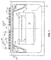
- the vacuum processing chamber 10 includes a substrate holder 12 providing an RF bias to a substrate supported thereon and a mechanical clamp 14 for clamping the substrate while it is He backcooled.
- a source of energy for maintaining a high density (e.g 10 17 -10 18 ions/m 3 (10 11 -10 12 ) (ions/cm 3 )) plasma in the chamber such as an antenna 18 powered by a suitable RF source and suitable RF impedance matching circuitry inductively couples RF energy into the chamber 10 so as to provide a high density plasma.
- the chamber includes suitable vacuum pumping apparatus for maintaining the interior of the chamber at a desired pressure (e.g.
- a substantially planar dielectric window 20 of uniform thickness is provided between the antenna 18 and the interior of the processing chamber 10 and forms the vacuum wall at the top of the processing chamber 10.
- a gas distribution plate commonly called a showerhead 22, is provided beneath the window 20 and includes a plurality of openings such as circular holes (not shown) for delivering process gas supplied by the gas supply 23 to the processing chamber 10.
- the gas distribution plate 22 can be omitted and process gas can be supplied to the chamber by other arrangements such as gas rings, etc.
- the antenna 18, according to one embodiment of the present invention is provided with a channel 24 through which a temperature control fluid is passed via inlet and outlet conduits 25,26.
- the antenna 18 and/or window 20 could be cooled by other techniques such as by blowing air over the antenna and window, passing a cooling medium through or in heat transfer contact with the window and/or gas distribution plate, etc.
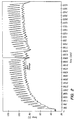
- FIG. 2 is a graph of time versus temperature which illustrates the effect of process drift on an oxide etch profile.
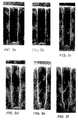
- FIGS. 3a-f the etch profiles of the etched substrates which are shown in the six photomicrographs change over time when substrates are processed consecutively.
- the second (FIG. 3a) and sixth substrates (FIG. 3b) to be etched have etch walls which are seen in cross section to be almost vertical.
- the 12th FIG.
- the etch walls are less vertical.
- the process was delayed for a boat (i.e., wafer cassette) change and a transfer module reset. These delays caused breaks in the continuous processing of the substrates and resulted in the temperature drops shown on the graph. After the boat change and transfer module reset, the temperature of the processing chamber and the process window continued to rise.
- the etch profile of these substrates was distorted to a great degree. With such distortion of the etch profile, the contact holes which are being tched may not be etched completely through the oxide layer to the underlayer. The failure to etch all the way through the oxide layer can lead to final integrated circuit chips which are inoperative.
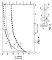
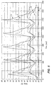
- FIG. 4 is a graph of parameters in the apparatus shown in FIG. 1 during a run of 25 silicon semiconductor wafers wherein selectivities are shown on the right side of the graph and temperatures at various locations of an aluminum nitride window are shown on the left side of the graph.
- the window was cooled by blowing air against the antenna and window at a rate of 7.1 x 10 -2 m 3 /s (150 cubic feet per minute).
- Curve A shows the temperature of the center of the window
- curve B shows the temperature of an outer edge of the window
- curve C shows the temperature at a location between the center and edge of the window.
- Curve D shows the selectivity at the center of the wafer and curve E shows the selectivity at an outer edge of the wafer.
- test results shown in FIG. 4 were carried out in an inductively coupled plasma reactor having an aluminum nitride window (similar to the arrangement shown in FIG. 1 but with a 0.25 m (10 inch) hole in the center of the gas distribution plate to expose the window) cooled by passing air over a spiral antenna spaced 0.004 m (0.14 inch) above an outer surface of the window.
- the antenna was supplied with 13.56 MHz RF power and the RF biasing electrode in the substrate support was supplied with 4 MHz RF power.
- the window temperatures did not increase above 343°K (120°C) as shown in FIG. 3.
- the processing of the wafers included a 90 second oxide etch using 4.2 x 10 -7 m 3 s -1 (25 sccm) C 2 HF 5 and 2.5 x 10 -7 m 3 s -1 (15 sccm) CHF 3 with 1100 watts applied to the antenna, 1300 watts applied to the bottom RF biasing electrode in the substrate support, a chamber pressure of 0.67 Pa (5 mTorr), and the bottom electrode at 263°K (10°C).
- the oxide etch was followed by a 10 seconds ashing step using 1.25 x 10 -5 m 3 s -1 (750 sccm) O 2 with 400 watts applied to the antenna and 100 watts applied to the RF biasing electrode and a chamber pressure of 15.5 mTorr followed by a second ashing step for 50 seconds using 1.25 x 10 -5 m 3 s -1 (750 sccm) O 2 with 400 watts applied to the antenna and 40 watts RF biasing power. Ashing, however, was omitted on wafer Nos. 2, 6, 12, 18 and 25. Including transport and other overhead operations, the cycle time was about 230 seconds per wafer. Probes were used to measure the window temperature at radii of 0.017 m (0.68 inches) and 0.14m (5.68 inches).
- FIG. 5 is a graph of window temperatures during a run of 5 wafers in the apparatus shown in FIG. 1.
- the window was cooled by passing a dielectric liquid at about 293°K (20°C) through a channel in the antenna while powering the antenna at about 1850 watts and powering an RF biasing electrode in the substrate support at about 2100 watts.
- a dielectric liquid at about 293°K (20°C)
- curve A shows the temperature at the center of the window
- curve B shows the temperature at a distance of 0.07m (2.75 inches) from the center of the window
- curve C shows the temperature at a distance of 0.13m (0.5 inch) from the center of the gas distribution plate
- curve D shows the temperature at a distance of 0.076m (3 inches) from the center of the plate
- curve E shows the temperature of coolant entering the antenna
- curve F shows the temperature of coolant exiting the antenna.
- a wafer is positioned on the substrate holder 12 and is typically held in place by an electrostatic clamp, a mechanical clamp, or other clamping mechanism when He backcooling is employed.
- Process gas is then supplied to the vacuum processing chamber 10 by passing the process gas through a gap between the window 20 and the gas distribution plate 22.
- a suitable gas distribution plate (i.e., showerhead) arrangement is disclosed in commonly owned U.S. Patent Application Serial No.08/509,080, the disclosure of which is hereby incorporated by reference.
- the window and gas distribution plate arrangement in FIG. 1 are planar and of uniform thickness, non-planar and/or non-uniform thickness geometries can be used for the window and/or gas distribution plate.
- a high density plasma is then ignited in the space between the wafer and the window by supplying suitable RF power to the antenna 18.
- a temperature control fluid is passed through the channel 24 in the antenna 18 to maintain the antenna 18, window 20 and gas distribution plate 22 at a temperature below a threshold temperature.
- the chamber pressure is typically below 40 Pa (300) (mTorr), preferably 0.27-5.3 Pa (2-40 mTorr), the antenna is powered at 200-2000 watts, preferably 400-1600 watts, theRE bias is ⁇ 2200 watts, preferably 1200-2200 watts, and the He backpressure is 666-5333 Pa (5-40 torr) preferably 933-2666 Pa (7-20Torr).
- the process gas can include 1.6 x 10 -7 -3.3 x 10 -6 m 3 s -1 (10-200 sccm) CHF 3 , 1.6 x 10 -7 -1.6 x 10 -6 m 3 s -1 (10-100 sccm) C 2 HF 5 and/or 1.6 x 10 -7 -1.6 x 10 -6 m 3 s -1 (10-100) C 2 F 6 .
- process drift may lead to changes in the oxide etch rate, the etch profile, and the etch selectivities and such process drift results from buildup of heat in the processing chamber as multiple substrates are consecutively processed. It has been discovered that if the temperature of the window 20 and/or gas distribution plate 22 in contact with the plasma processing the substrate can be maintained below the threshold temperature, the process drift can be substantially reduced.
- the temperatures of other surfaces of the interior of the vacuum processing chamber 10 such as conical ring 30 can also be temperature controlled so as to be below the threshold temperature.
- Temperature control of the gas distribution plate 22 can be provided by using channel 24 for circulating a fluid through the antenna 18 from a closed circuit temperature controller 28.
- the temperature controller preferably monitors the window temperature such as by one or more temperature sensors 27 and controls coolant temperature and/or flow rate of coolant through the antenna 18 to maintain the window below a threshold temperature.
- the antenna 18 is preferably in good thermal contact with the window 20 to provide adequate heat transfer between the window and the antenna 18.
- the window is made of a high thermal conductivity dielectric material such as aluminum nitride which maximizes heat transfer from the antenna 18 through the window to the gas distribution plate 22.
- the gas distribution plate 22 is also preferably made of a material having a high thermal conductivity, such as, aluminum nitride but other dielectric materials such as aluminum oxide or quartz can also be used for the gas distribution plate 22.
- the heat which is received by the gas distribution plate 22 due to ion bombardment from the plasma is passed through the window 20 and can be removed by passing cooling fluid within the antenna 18, increasing gas pressure between the window and gas distribution plate 22 and/or blowing cooling gas over the antenna.
- the antenna 18 can have various shapes and profiles such as a substantially planar profile and/or a spiral shape having one or more (e.g., 3 to 7) turns in the spiral.
- the channel 24 preferably extends through all portions of the antenna 18 from a cooling fluid inlet to a cooling fluid outlet.
- the cooling fluid may flow from the exterior of the spiral antenna 18 toward the center, or from the center to the exterior thereof.
- the antenna may be bonded to the window by any suitable technique such as brazing, adhesive (e.g., RTV), etc., which provides good heat transfer characteristics between the antenna and the window.
- the cooling fluid which is passed through the antenna is preferably a non-conducting liquid such as deionized water or Fluoroinert (a dielectric fluid made by DuPont).
- the antenna can include a cooling tube which is bonded to a surface, such as a top surface, of the antenna.
- the cooling fluid is passed through the cooling tube in the same manner as the channel 24.
- the window 20 and the gas distribution plate 22 may be formed as a single piece.
- higher thermal conductivity of the window/gas distribution plate 22 arrangement can be provided and/or the heat transfer across the window and the gas distribution plate 22 can be made more uniform.
- suitable gas passages and outlet holes can be provided in a green ceramic dielectric material which is later sintered to form a unitary plate.
- the dimensions of the passages and holes are preferably small enough to avoid conditions under which plasma would form during flow of process gas and powering of the antenna.
- the temperature of the gas distribution plate 22 can be controlled by controlling the temperature of the circulating fluid in the antenna 18.
- the temperature of the gas distribution plate 22 is desirably maintained below a threshold temperature.
- the threshold temperature can be 393°K (120°C) or less, preferably 363°K (90°C) or less, and more preferably 80°C or less such as by controlling the temperature of the circulating fluid with a closed circuit cooling system.
- the temperature of the window may also be controlled by modulating the pressure of the process gas behind the gas distribution plate 22 during the etching process. Additionally, the temperature may also be controlled by additional steps such as ashing steps in the process or during wafer transport which cause delays and allow cooling of the vacuum chamber and consequently the window/gas distribution plate 22 arrangement.
- the antenna may be desirable to locate the antenna such that portions thereof do not overlie any outlet holes in the gas distribution plate.
- the antenna comprises a multi-turn coil and the gas distribution plate includes a center hole and 6 holes located on a circle at a fixed radius from the center hole, the antenna is preferably located such that any turn passing through the circle is located equally between a pair of adjacent holes located on the circle. Such positioning of the antenna would minimize the possibility of striking a plasma in the holes located closest to the antenna.
- Dielectric plates used as windows into the vacuum environment of a process chamber are subject to atmospheric pressure of about 10 4 Kg/m 2 .
- process requirements may dictate that the inner surface of such a window be composed of a process compatible material, for its chemical and/or physical properties, e.g. quartz. This can therefore be prepared as a bulk window material, or prepared as a coating or bonded surface of sufficient thickness of some other material or composite structure, or prepared as a cover plate supported separately in the vacuum.
- the window design must be compatible with the structural requirements set forth above, or if a coating or bonding technique is employed, the composite structure will be susceptible to film tension effects in the growth or bonding process, and the possibility of differential thermal stress, and in the last case of a cover plate, a separate support structure may be required.
- the process requirements may dictate that the surface temperature of the chamber walls possibly including the inner surface of any dielectric window or cover plate thereto affixed, be constrained, and possibly actively controlled.
- Windows into process chambers are usually used for the transmission of energy into, or from the process chamber.
- power in the form of U-V, visible, I-R, microwave and RF E-M radiation are all transmitted into and from vacuum chambers using dielectric windows. If significant power is transmitted in this way, the dielectric may become heated by loss processes depending on the frequency ( ⁇ ), and the loss factor (tan ⁇ ). Even if transmission loss heating is negligible, the window constitutes a wall of the process chamber and may be heated by radiation, convection and conduction processes from the components and process materials in the chamber.
- TCP transmission coupled plasma
- several. watts can be dissipated on every square cm of the window's inner surface. If the window is made of bulk quartz material 0.02 m (2 cm) thick, this will result in an unavoidable temperature rise of the inner surface of several hundred °C.
- Quartz can be used as the window material since it is compatible with many process regimes and has good thermal shock resistance due to its low coefficient of thermal expansion. However, it only has moderate mechanical properties, extremely low thermal conductivity leading to high temperature gradients, and high differential expansion stress when in contact with materials having significantly different coefficients of thermal expansion. Materials having a combination of such properties can be utilized in a composite window according to a further aspect of the invention.
- a composite window can be provided with a process compatible material such as quartz as its inner surface and/or the window can be constructed in a manner such that the inner surface can be temperature monitored with the temperature thereof being passively or actively controlled.
- the bulk material of the window for its vacuum compatibility, dielectric properties, relative process inertness, mechanical and thermal properties.
- aluminum nitride is fairly inert, has good dielectric properties (low dielectric constant and loss factor), has mechanical properties similar to alumina including thermal expansion, and thermal capacity, but has thermal conductivity approximately five times greater than alumina, i.e. two orders of magnitude greater than that of quartz.
- Such a window will only support a temperature gradient of about 274°K (1°C) across it for each watt/cm 2 dissipated, will have a rather short thermal time constant (seconds rather than minutes), and will therefore still be fairly good with regard to thermal shock.
- it is possible to control the inside temperature of the window by monitoring the temperature of the outside and heating or cooling the outside selectively, since the inside surface will closely follow suit, unlike the case of a bulk quartz window for instance.
- a relatively thin, e.g., about 2 x 10 -3 m (2 mm) thick, sub-plate comprising one or more layers of which the exposed layer is of process compatible material can be supported in close proximity to the lower surface of, and concentric with the main window plate.
- Such a plate even if made of quartz, for instance, will only account for a temperature differential across its thickness of some tens of degrecs instead of hundreds of degrees as was the case for the 1 x 10 -2 m (2 cm) thick quartz window when subjected to the same thermal flux.
- the outside of the sub-plate may be separated from the outer window by a vacuum, and even though the plate is in close proximity to the outer window, it is not in intimate thermal contact with the main window plate, such that a large temperature differential could be built up across the interspace between them.
- a thin film of thermally conductive contact medium can be employed to minimize the temperature drop across the interspace. If the medium is fluid or elastic, excessive rigidity can be avoided, such that no large differential expansion forces will be set up.
- the mechanical support of such a sub-plate adjacent to the main window can be arranged, as shown in FIG. 6, such that there is only a small leakage path 40, if any, from the interspace 42 between the main window plate 44 and the sub-plate 46 into the chamber 48 proper, an elastomer edge seal 50,52 being provided if necessary for use with a fluid thermal contact medium.
- the interspace 42 can be filled with an inert thermal contact medium such as vacuum grease, a thin silicone rubber film, or most conveniently with a gas.
- the gas is preferably a light inert gas at a pressure which optimizes thermal conductance since the gas is not being used for convective transport, e.g., He at about 1333 Pa (10 Torr), being typical, depending on gap dimensions and mean free path considerations.
- a gas is the contact medium, an inlet, and, if required, an outlet also, are arranged such that the interspace 42 can be filled to the appropriate pressure via a suitable gas supply passage such as passage 54.
- the He pressure which can be two orders or magnitude below atmospheric pressure must be supported by the sub-plate, or if grease or a film is used as the contact medium, provision can be made to vent any trapped or included gas and to allow for the relief of thermal expansion forces.
- the contact medium can comprise the process gas or a gas added to the process gas.
- the openings in the gas distribution plate can be sized so as to optimize pressure in the interspace and improve heat transfer from the sub-plate to the main window.
- the gas pressure in the interspace between the window and gas distribution plate can be regulated within a range of 133-13,324 Pa (1-100Torr).
- the complete assembly consisting of a sandwich of main window plate, thin film of thermal conductor (be it semi-solid, or fluid), and sub-plate, will allow monitoring and temperature control of the inside surface facing the chamber by means of contact with the outside of the main window by virtue of the greatly improved thermal conductance between inside and outside surfaces when compared with a solid window of the sub-plate material, e.g. quartz, capable of performing the same structural function.
- the outside temperature can be monitored by standard thermometric techniques, both contacting and otherwise. Temperature control can be achieved using embedded, contact or radiant, heater elements, and/or forced fluid (liquid or gas) on the exposed surface of the main window.
- Simultaneous continuous direct temperature monitoring and precision control of the inside surface may not be possible from the outside alone, although knowledge of the thermal characteristics and recent history of the double plate window can be utilized. For instance, pulsing the feedback control system to observe the dynamic response of monitoring sensors in various positions on the window would be one technique, while another might employ sensors inserted into the main window sub-plate interspace.
Abstract
Description
Claims (26)
- A method of processing a substrate in a plasma processing chamber (10) whilst controlling the temperature of the plasma processing chamber (10); said method comprising:placing a substrate on a substrate holder (12) in the processing chamber wherein an interior surface of a dielectric member (20) made of high thermal conductivity material or comprising high thermal conductivity material and an inner surface of process compatible material and forming a wall of the processing chamber faces the substrate holder;processing the substrate by supplying process gas to the processing chamber and energizing the process gas into a plasma state by inductively coupling RF energy through the dielectric member into the processing chamber;operating a cooling mechanism to cool the dielectric member to maintain the interior surface thereof below a threshold temperature during the processing of the substrate; andconsecutively processing substrates in the processing chamber by contacting the substrates with plasma gas while maintaining the interior surface below the threshold temperature.
- A method according to claim 1 wherein the processing chamber includes a substantially planar antenna (18), the process gas being energized into the plasma state by supplying RF power to the antenna, and the step of cooling being carried out by passing a temperature controlling fluid in contact with the dielectric member or the antenna.
- A method according to claim 2 wherein the step of cooling is carried out by passing an aqueous or non-aqueous electrically non-conducting liquid through a channel (24) in the antenna.
- A method according to claim 2 or 3 wherein the liquid is passed through the antenna by a closed circuit cooling system.
- A method according to any one of the preceding claims wherein the processing comprises etching and the threshold temperature is less than or equal to 90°C.
- A method according to any one of the preceding claims wherein the plasma comprises a high density plasma and the substrates are processed by etching an oxide layer on the substrates with the high density plasma while applying an RF bias to the substrates.
- A method according to any one of the preceding claims wherein the dielectric member comprises a dielectric window and the processing comprises plasma etching a masked layer on each of the substrates.
- A method according to any one of the preceding claims wherein the dielectric member comprises a dielectric window having first and second sections separated from each other by a gap, the first section including an outer surface exposed to ambient pressure and the second section including the interior surface, the cooling step being carried out by providing a heat transfer medium in the gap.
- A method according to claim 2 wherein the dielectric member comprises a gas distribution plate (22), the temperature of the gas distribution plate being maintained below the threshold temperature by passing the temperature controlling fluid through the antenna.
- A plasma processing chamber (10) comprising:a substrate holder (12) for supporting a substrate within the processing chamber;a dielectric member (20) made of high thermal conductivity material or comprising high thermal conductivity material and an inner surface of process compatible material and having an interior surface thereof facing the substrate holder;a gas supply supplying process gas to the chamber;an RF energy source (19) which inductively couples RF energy through the dielectric member and into the chamber to energize the process gas into a plasma state; anda cooling mechanism which cools the dielectric member and maintains the interior surface below a threshold temperature.
- A chamber according to claim 10 wherein the dielectric member comprises a gas distribution plate (22) having a plurality of holes therethrough supplying the process gas to the interior of the chamber and the gas supply supplies gas to the gas distribution plate.
- A chamber according to claim 10 wherein the dielectric member includes a dielectric window (20) and the RF energy source comprises a substantially planar antenna (18) adjacent the window, the antenna supplying RF power through the window to energize process gas in the processing chamber into a plasma state.
- A chamber according to claim 10 wherein the chamber includes a dielectric window (20) and the RF energy source comprises an antenna (18) adjacent the window, the antenna supplying RF power through the window to energize process gas in the processing chamber into a plasma state, the interior surface comprising an inner surface of the window and the cooling mechanism including a closed circuit temperature controller (28) and a channel (24) in the antenna through which a temperature controlling fluid is circulated.
- A chamber according to claim 10 wherein the dielectric member comprises a dielectric window having first and second sections (44, 46) separated from each other by a gap (42), the first section including an outer surface exposed to ambient pressure and the second section including the interior surface, the gap being filled with a heat transfer medium.
- A chamber according to claim 14 wherein the heat transfer medium is a coolant and the cooling mechanism circulates the coolant in the gap.
- A chamber according to claim 10 wherein the chamber includes a dielectric window (20), the RF energy source comprises a substantially planar antenna (18) adjacent the window, the antenna supplying RF power through the window to energize process gas in the processing chamber into a plasma state and the dielectric member comprises a dielectric gas distribution plate (22) with the dielectric window disposed between the antenna and the gas distribution plate.
- A chamber according to claim 16 wherein the window comprises a unitary body of alumina or aluminium nitride.
- A chamber according to claim 16 wherein the cooling mechanism passes a temperature controlling fluid in heat transfer contact with the antenna or the gas distribution plate.
- A chamber according to claim 10 and further comprising a closed circuit cooling system which supplies an electrically non-conducting cooling liquid to the cooling mechanism.
- A chamber according to claim 13, 18 or 19 wherein the fluid or liquid is a non-aqueous dielectric.
- A chamber according to claim 10 wherein the RF energy source (19) is thermally coupled to the dielectric member (20) and the dielectric member consists essentially of aluminium nitride or alumina.
- A chamber according to claim 10 wherein the dielectric member comprises a unitary body of Al2O3 or AIN.
- A chamber according to claim 10 wherein the dielectric member is in thermal contact with the RF energy source.
- A chamber according to claim 10 wherein the plasma processing chamber comprises a plasma etching reactor and the cooling mechanism maintains the interior surface of the dielectric member at a temperature less than a temperature at which process drift occurs.
- A chamber according to claim 10 wherein the cooling mechanism includes one or more sensors (27) monitoring the temperature of an exterior surface of the dielectric member and the cooling mechanism maintains the interior surface of the dielectric member below the threshold temperature based on output from the one or more sensors.
- A chamber according to claim 10 wherein the dielectric member consists essentially of a material having thermal conductivity of at least 20 W/m-K.
Applications Claiming Priority (3)
| Application Number | Priority Date | Filing Date | Title |
|---|---|---|---|
| US658259 | 1996-06-05 | ||
| US08/658,259 US5863376A (en) | 1996-06-05 | 1996-06-05 | Temperature controlling method and apparatus for a plasma processing chamber |
| PCT/US1997/009031 WO1997046730A1 (en) | 1996-06-05 | 1997-06-02 | Temperature controlling method and apparatus for a plasma processing chamber |
Publications (2)
| Publication Number | Publication Date |
|---|---|
| EP0910686A1 EP0910686A1 (en) | 1999-04-28 |
| EP0910686B1 true EP0910686B1 (en) | 2003-01-08 |
Family
ID=24640537
Family Applications (1)
| Application Number | Title | Priority Date | Filing Date |
|---|---|---|---|
| EP97925746A Expired - Lifetime EP0910686B1 (en) | 1996-06-05 | 1997-06-02 | Temperature controlling method and apparatus for a plasma processing chamber |
Country Status (9)
| Country | Link |
|---|---|
| US (1) | US5863376A (en) |
| EP (1) | EP0910686B1 (en) |
| JP (1) | JP4166831B2 (en) |
| CN (1) | CN1104511C (en) |
| AT (1) | ATE230811T1 (en) |
| AU (1) | AU3079597A (en) |
| DE (1) | DE69718321T2 (en) |
| IL (1) | IL127357A (en) |
| WO (1) | WO1997046730A1 (en) |
Families Citing this family (170)
| Publication number | Priority date | Publication date | Assignee | Title |
|---|---|---|---|---|
| US6231776B1 (en) | 1995-12-04 | 2001-05-15 | Daniel L. Flamm | Multi-temperature processing |
| US5711851A (en) * | 1996-07-12 | 1998-01-27 | Micron Technology, Inc. | Process for improving the performance of a temperature-sensitive etch process |
| JP2921499B2 (en) * | 1996-07-30 | 1999-07-19 | 日本電気株式会社 | Plasma processing equipment |
| US5993594A (en) | 1996-09-30 | 1999-11-30 | Lam Research Corporation | Particle controlling method and apparatus for a plasma processing chamber |
| US6464843B1 (en) * | 1998-03-31 | 2002-10-15 | Lam Research Corporation | Contamination controlling method and apparatus for a plasma processing chamber |
| EP1145276A1 (en) * | 1998-12-30 | 2001-10-17 | Lam Research Corporation | Method and apparatus for etch rate stabilization |
| US6502529B2 (en) | 1999-05-27 | 2003-01-07 | Applied Materials Inc. | Chamber having improved gas energizer and method |
| US6916399B1 (en) | 1999-06-03 | 2005-07-12 | Applied Materials Inc | Temperature controlled window with a fluid supply system |
| US6444083B1 (en) | 1999-06-30 | 2002-09-03 | Lam Research Corporation | Corrosion resistant component of semiconductor processing equipment and method of manufacturing thereof |
| US6227140B1 (en) | 1999-09-23 | 2001-05-08 | Lam Research Corporation | Semiconductor processing equipment having radiant heated ceramic liner |
| US6408786B1 (en) | 1999-09-23 | 2002-06-25 | Lam Research Corporation | Semiconductor processing equipment having tiled ceramic liner |
| KR100806097B1 (en) * | 1999-09-30 | 2008-02-21 | 램 리써치 코포레이션 | Pretreated gas distribution plate |
| US6673198B1 (en) * | 1999-12-22 | 2004-01-06 | Lam Research Corporation | Semiconductor processing equipment having improved process drift control |
| JP3379506B2 (en) * | 2000-02-23 | 2003-02-24 | 松下電器産業株式会社 | Plasma processing method and apparatus |
| US6528751B1 (en) | 2000-03-17 | 2003-03-04 | Applied Materials, Inc. | Plasma reactor with overhead RF electrode tuned to the plasma |
| US8048806B2 (en) * | 2000-03-17 | 2011-11-01 | Applied Materials, Inc. | Methods to avoid unstable plasma states during a process transition |
| US6894245B2 (en) * | 2000-03-17 | 2005-05-17 | Applied Materials, Inc. | Merie plasma reactor with overhead RF electrode tuned to the plasma with arcing suppression |
| US7220937B2 (en) * | 2000-03-17 | 2007-05-22 | Applied Materials, Inc. | Plasma reactor with overhead RF source power electrode with low loss, low arcing tendency and low contamination |
| US6900596B2 (en) | 2002-07-09 | 2005-05-31 | Applied Materials, Inc. | Capacitively coupled plasma reactor with uniform radial distribution of plasma |
| US7196283B2 (en) | 2000-03-17 | 2007-03-27 | Applied Materials, Inc. | Plasma reactor overhead source power electrode with low arcing tendency, cylindrical gas outlets and shaped surface |
| US20070048882A1 (en) * | 2000-03-17 | 2007-03-01 | Applied Materials, Inc. | Method to reduce plasma-induced charging damage |
| US8617351B2 (en) | 2002-07-09 | 2013-12-31 | Applied Materials, Inc. | Plasma reactor with minimal D.C. coils for cusp, solenoid and mirror fields for plasma uniformity and device damage reduction |
| US7141757B2 (en) * | 2000-03-17 | 2006-11-28 | Applied Materials, Inc. | Plasma reactor with overhead RF source power electrode having a resonance that is virtually pressure independent |
| US7030335B2 (en) * | 2000-03-17 | 2006-04-18 | Applied Materials, Inc. | Plasma reactor with overhead RF electrode tuned to the plasma with arcing suppression |
| US6890861B1 (en) | 2000-06-30 | 2005-05-10 | Lam Research Corporation | Semiconductor processing equipment having improved particle performance |
| US6506254B1 (en) | 2000-06-30 | 2003-01-14 | Lam Research Corporation | Semiconductor processing equipment having improved particle performance |
| US20020185226A1 (en) * | 2000-08-10 | 2002-12-12 | Lea Leslie Michael | Plasma processing apparatus |
| US7270724B2 (en) | 2000-12-13 | 2007-09-18 | Uvtech Systems, Inc. | Scanning plasma reactor |
| US6790242B2 (en) | 2000-12-29 | 2004-09-14 | Lam Research Corporation | Fullerene coated component of semiconductor processing equipment and method of manufacturing thereof |
| US6620520B2 (en) * | 2000-12-29 | 2003-09-16 | Lam Research Corporation | Zirconia toughened ceramic components and coatings in semiconductor processing equipment and method of manufacture thereof |
| US6533910B2 (en) | 2000-12-29 | 2003-03-18 | Lam Research Corporation | Carbonitride coated component of semiconductor processing equipment and method of manufacturing thereof |
| US6613442B2 (en) * | 2000-12-29 | 2003-09-02 | Lam Research Corporation | Boron nitride/yttria composite components of semiconductor processing equipment and method of manufacturing thereof |
| US6537429B2 (en) | 2000-12-29 | 2003-03-25 | Lam Research Corporation | Diamond coatings on reactor wall and method of manufacturing thereof |
| US7128804B2 (en) * | 2000-12-29 | 2006-10-31 | Lam Research Corporation | Corrosion resistant component of semiconductor processing equipment and method of manufacture thereof |
| US6805952B2 (en) | 2000-12-29 | 2004-10-19 | Lam Research Corporation | Low contamination plasma chamber components and methods for making the same |
| US6773683B2 (en) * | 2001-01-08 | 2004-08-10 | Uvtech Systems, Inc. | Photocatalytic reactor system for treating flue effluents |
| US6830622B2 (en) * | 2001-03-30 | 2004-12-14 | Lam Research Corporation | Cerium oxide containing ceramic components and coatings in semiconductor processing equipment and methods of manufacture thereof |
| US6527911B1 (en) * | 2001-06-29 | 2003-03-04 | Lam Research Corporation | Configurable plasma volume etch chamber |
| JP3876167B2 (en) * | 2002-02-13 | 2007-01-31 | 川崎マイクロエレクトロニクス株式会社 | Cleaning method and semiconductor device manufacturing method |
| US6780787B2 (en) | 2002-03-21 | 2004-08-24 | Lam Research Corporation | Low contamination components for semiconductor processing apparatus and methods for making components |
| US7311797B2 (en) * | 2002-06-27 | 2007-12-25 | Lam Research Corporation | Productivity enhancing thermal sprayed yttria-containing coating for plasma reactor |
| TWI283899B (en) * | 2002-07-09 | 2007-07-11 | Applied Materials Inc | Capacitively coupled plasma reactor with magnetic plasma control |
| US7569497B2 (en) * | 2002-07-30 | 2009-08-04 | Tokyo Electron Limited | Method and apparatus for forming insulating layer |
| KR100468203B1 (en) * | 2002-08-16 | 2005-01-26 | 어댑티브프라즈마테크놀로지 주식회사 | Apparatus and Method for controlling temperature of dome in Plasma etching system |
| US7247218B2 (en) | 2003-05-16 | 2007-07-24 | Applied Materials, Inc. | Plasma density, energy and etch rate measurements at bias power input and real time feedback control of plasma source and bias power |
| US7470626B2 (en) * | 2003-05-16 | 2008-12-30 | Applied Materials, Inc. | Method of characterizing a chamber based upon concurrent behavior of selected plasma parameters as a function of source power, bias power and chamber pressure |
| US7795153B2 (en) * | 2003-05-16 | 2010-09-14 | Applied Materials, Inc. | Method of controlling a chamber based upon predetermined concurrent behavior of selected plasma parameters as a function of selected chamber parameters |
| US7452824B2 (en) * | 2003-05-16 | 2008-11-18 | Applied Materials, Inc. | Method of characterizing a chamber based upon concurrent behavior of selected plasma parameters as a function of plural chamber parameters |
| US7910013B2 (en) | 2003-05-16 | 2011-03-22 | Applied Materials, Inc. | Method of controlling a chamber based upon predetermined concurrent behavior of selected plasma parameters as a function of source power, bias power and chamber pressure |
| US7901952B2 (en) * | 2003-05-16 | 2011-03-08 | Applied Materials, Inc. | Plasma reactor control by translating desired values of M plasma parameters to values of N chamber parameters |
| US8540843B2 (en) | 2004-06-30 | 2013-09-24 | Lam Research Corporation | Plasma chamber top piece assembly |
| US7780791B2 (en) * | 2004-06-30 | 2010-08-24 | Lam Research Corporation | Apparatus for an optimized plasma chamber top piece |
| US20060000551A1 (en) * | 2004-06-30 | 2006-01-05 | Saldana Miguel A | Methods and apparatus for optimal temperature control in a plasma processing system |
| US7323116B2 (en) * | 2004-09-27 | 2008-01-29 | Lam Research Corporation | Methods and apparatus for monitoring a process in a plasma processing system by measuring self-bias voltage |
| US20060065631A1 (en) * | 2004-09-27 | 2006-03-30 | Chia-Cheng Cheng | Methods and apparatus for monitoring a process in a plasma processing system by measuring impedance |
| US20060065632A1 (en) * | 2004-09-27 | 2006-03-30 | Chia-Cheng Cheng | Methods and apparatus for monitoring a process in a plasma processing system by measuring a plasma frequency |
| US7396431B2 (en) * | 2004-09-30 | 2008-07-08 | Tokyo Electron Limited | Plasma processing system for treating a substrate |
| US20060081185A1 (en) * | 2004-10-15 | 2006-04-20 | Justin Mauck | Thermal management of dielectric components in a plasma discharge device |
| US7359177B2 (en) * | 2005-05-10 | 2008-04-15 | Applied Materials, Inc. | Dual bias frequency plasma reactor with feedback control of E.S.C. voltage using wafer voltage measurement at the bias supply output |
| US7445726B2 (en) * | 2005-09-05 | 2008-11-04 | United Microelectronics Corp. | Photoresist trimming process |
| AT502351A1 (en) * | 2005-09-12 | 2007-03-15 | Ziger Peter | APPENDIX FOR THE PLASMA PROCESSING OF ENDLESS MATERIAL |
| US20080083732A1 (en) * | 2006-10-10 | 2008-04-10 | Sumitomo Electric Industries, Ltd. | Wafer holder and exposure apparatus equipped with wafer holder |
| US8097105B2 (en) * | 2007-01-11 | 2012-01-17 | Lam Research Corporation | Extending lifetime of yttrium oxide as a plasma chamber material |
| US7972471B2 (en) * | 2007-06-29 | 2011-07-05 | Lam Research Corporation | Inductively coupled dual zone processing chamber with single planar antenna |
| US8449786B2 (en) * | 2007-12-19 | 2013-05-28 | Lam Research Corporation | Film adhesive for semiconductor vacuum processing apparatus |
| SG187386A1 (en) | 2007-12-19 | 2013-02-28 | Lam Res Corp | A composite showerhead electrode assembly for a plasma processing apparatus |
| JP5710267B2 (en) | 2007-12-21 | 2015-04-30 | ラム リサーチ コーポレーションLam Research Corporation | Silicon deep etching with silicon structure fabrication and profile control |
| JP5444218B2 (en) * | 2008-07-04 | 2014-03-19 | 東京エレクトロン株式会社 | Plasma processing apparatus and temperature adjustment mechanism of dielectric window |
| US8173547B2 (en) | 2008-10-23 | 2012-05-08 | Lam Research Corporation | Silicon etch with passivation using plasma enhanced oxidation |
| KR200475462Y1 (en) * | 2009-03-27 | 2014-12-03 | 램 리써치 코포레이션 | Replaceable upper chamber section of plasma processing apparatus |
| JP5309213B2 (en) * | 2009-08-25 | 2013-10-09 | キヤノンアネルバ株式会社 | Plasma processing apparatus and device manufacturing method |
| US9076634B2 (en) * | 2009-09-10 | 2015-07-07 | Lam Research Corporation | Replaceable upper chamber parts of plasma processing apparatus |
| US20110278260A1 (en) | 2010-05-14 | 2011-11-17 | Applied Materials, Inc. | Inductive plasma source with metallic shower head using b-field concentrator |
| US10283321B2 (en) | 2011-01-18 | 2019-05-07 | Applied Materials, Inc. | Semiconductor processing system and methods using capacitively coupled plasma |
| KR101208567B1 (en) | 2011-02-08 | 2012-12-06 | 엘아이지에이디피 주식회사 | Upper Lid for substrate processing apparatus |
| US9064815B2 (en) | 2011-03-14 | 2015-06-23 | Applied Materials, Inc. | Methods for etch of metal and metal-oxide films |
| US9978565B2 (en) * | 2011-10-07 | 2018-05-22 | Lam Research Corporation | Systems for cooling RF heated chamber components |
| US8904887B2 (en) * | 2011-11-17 | 2014-12-09 | The Aerospace Corporation | Radio frequency transparent thermal window |
| CN103515179B (en) * | 2012-06-29 | 2016-02-10 | 北京北方微电子基地设备工艺研究中心有限责任公司 | Plasma-reaction-chamber and there is its plasma device |
| US9267739B2 (en) | 2012-07-18 | 2016-02-23 | Applied Materials, Inc. | Pedestal with multi-zone temperature control and multiple purge capabilities |
| US9373517B2 (en) | 2012-08-02 | 2016-06-21 | Applied Materials, Inc. | Semiconductor processing with DC assisted RF power for improved control |
| CN103681410B (en) * | 2012-08-31 | 2016-08-31 | 细美事有限公司 | For processing the device of substrate |
| US9132436B2 (en) | 2012-09-21 | 2015-09-15 | Applied Materials, Inc. | Chemical control features in wafer process equipment |
| CN103794457B (en) * | 2012-10-29 | 2016-08-03 | 中微半导体设备(上海)有限公司 | A kind of apparatus for processing plasma and temperature isolation device therein |
| US8970114B2 (en) | 2013-02-01 | 2015-03-03 | Lam Research Corporation | Temperature controlled window of a plasma processing chamber component |
| US10256079B2 (en) | 2013-02-08 | 2019-04-09 | Applied Materials, Inc. | Semiconductor processing systems having multiple plasma configurations |
| US9362130B2 (en) | 2013-03-01 | 2016-06-07 | Applied Materials, Inc. | Enhanced etching processes using remote plasma sources |
| US20140356985A1 (en) | 2013-06-03 | 2014-12-04 | Lam Research Corporation | Temperature controlled substrate support assembly |
| KR102262657B1 (en) | 2014-10-13 | 2021-06-08 | 삼성전자주식회사 | Plasma processing device |
| US9355922B2 (en) | 2014-10-14 | 2016-05-31 | Applied Materials, Inc. | Systems and methods for internal surface conditioning in plasma processing equipment |
| US9966240B2 (en) | 2014-10-14 | 2018-05-08 | Applied Materials, Inc. | Systems and methods for internal surface conditioning assessment in plasma processing equipment |
| US11637002B2 (en) | 2014-11-26 | 2023-04-25 | Applied Materials, Inc. | Methods and systems to enhance process uniformity |
| US10573496B2 (en) | 2014-12-09 | 2020-02-25 | Applied Materials, Inc. | Direct outlet toroidal plasma source |
| US10224210B2 (en) | 2014-12-09 | 2019-03-05 | Applied Materials, Inc. | Plasma processing system with direct outlet toroidal plasma source |
| US11257693B2 (en) | 2015-01-09 | 2022-02-22 | Applied Materials, Inc. | Methods and systems to improve pedestal temperature control |
| US9728437B2 (en) | 2015-02-03 | 2017-08-08 | Applied Materials, Inc. | High temperature chuck for plasma processing systems |
| US20160225652A1 (en) | 2015-02-03 | 2016-08-04 | Applied Materials, Inc. | Low temperature chuck for plasma processing systems |
| US9881805B2 (en) | 2015-03-02 | 2018-01-30 | Applied Materials, Inc. | Silicon selective removal |
| US9691645B2 (en) | 2015-08-06 | 2017-06-27 | Applied Materials, Inc. | Bolted wafer chuck thermal management systems and methods for wafer processing systems |
| US9741593B2 (en) | 2015-08-06 | 2017-08-22 | Applied Materials, Inc. | Thermal management systems and methods for wafer processing systems |
| US9349605B1 (en) | 2015-08-07 | 2016-05-24 | Applied Materials, Inc. | Oxide etch selectivity systems and methods |
| US10504700B2 (en) | 2015-08-27 | 2019-12-10 | Applied Materials, Inc. | Plasma etching systems and methods with secondary plasma injection |
| US10504754B2 (en) | 2016-05-19 | 2019-12-10 | Applied Materials, Inc. | Systems and methods for improved semiconductor etching and component protection |
| US10522371B2 (en) | 2016-05-19 | 2019-12-31 | Applied Materials, Inc. | Systems and methods for improved semiconductor etching and component protection |
| US9865484B1 (en) | 2016-06-29 | 2018-01-09 | Applied Materials, Inc. | Selective etch using material modification and RF pulsing |
| US10403474B2 (en) * | 2016-07-11 | 2019-09-03 | Lam Research Corporation | Collar, conical showerheads and/or top plates for reducing recirculation in a substrate processing system |
| US10062575B2 (en) | 2016-09-09 | 2018-08-28 | Applied Materials, Inc. | Poly directional etch by oxidation |
| US10629473B2 (en) | 2016-09-09 | 2020-04-21 | Applied Materials, Inc. | Footing removal for nitride spacer |
| US9934942B1 (en) * | 2016-10-04 | 2018-04-03 | Applied Materials, Inc. | Chamber with flow-through source |
| US10062585B2 (en) | 2016-10-04 | 2018-08-28 | Applied Materials, Inc. | Oxygen compatible plasma source |
| US10546729B2 (en) | 2016-10-04 | 2020-01-28 | Applied Materials, Inc. | Dual-channel showerhead with improved profile |
| US10062579B2 (en) | 2016-10-07 | 2018-08-28 | Applied Materials, Inc. | Selective SiN lateral recess |
| US9947549B1 (en) | 2016-10-10 | 2018-04-17 | Applied Materials, Inc. | Cobalt-containing material removal |
| US9768034B1 (en) | 2016-11-11 | 2017-09-19 | Applied Materials, Inc. | Removal methods for high aspect ratio structures |
| US10163696B2 (en) | 2016-11-11 | 2018-12-25 | Applied Materials, Inc. | Selective cobalt removal for bottom up gapfill |
| US10242908B2 (en) | 2016-11-14 | 2019-03-26 | Applied Materials, Inc. | Airgap formation with damage-free copper |
| US10026621B2 (en) | 2016-11-14 | 2018-07-17 | Applied Materials, Inc. | SiN spacer profile patterning |
| US10566206B2 (en) | 2016-12-27 | 2020-02-18 | Applied Materials, Inc. | Systems and methods for anisotropic material breakthrough |
| US10403507B2 (en) | 2017-02-03 | 2019-09-03 | Applied Materials, Inc. | Shaped etch profile with oxidation |
| US10431429B2 (en) | 2017-02-03 | 2019-10-01 | Applied Materials, Inc. | Systems and methods for radial and azimuthal control of plasma uniformity |
| US10043684B1 (en) | 2017-02-06 | 2018-08-07 | Applied Materials, Inc. | Self-limiting atomic thermal etching systems and methods |
| US10319739B2 (en) | 2017-02-08 | 2019-06-11 | Applied Materials, Inc. | Accommodating imperfectly aligned memory holes |
| US20180235110A1 (en) * | 2017-02-16 | 2018-08-16 | Lam Research Corporation | Cooling system for rf power electronics |
| US10943834B2 (en) | 2017-03-13 | 2021-03-09 | Applied Materials, Inc. | Replacement contact process |
| US10319649B2 (en) | 2017-04-11 | 2019-06-11 | Applied Materials, Inc. | Optical emission spectroscopy (OES) for remote plasma monitoring |
| US10312475B2 (en) * | 2017-05-15 | 2019-06-04 | Applied Materials, Inc. | CVD thin film stress control method for display application |
| US11276559B2 (en) | 2017-05-17 | 2022-03-15 | Applied Materials, Inc. | Semiconductor processing chamber for multiple precursor flow |
| US11276590B2 (en) | 2017-05-17 | 2022-03-15 | Applied Materials, Inc. | Multi-zone semiconductor substrate supports |
| US10497579B2 (en) | 2017-05-31 | 2019-12-03 | Applied Materials, Inc. | Water-free etching methods |
| US10049891B1 (en) | 2017-05-31 | 2018-08-14 | Applied Materials, Inc. | Selective in situ cobalt residue removal |
| US10920320B2 (en) | 2017-06-16 | 2021-02-16 | Applied Materials, Inc. | Plasma health determination in semiconductor substrate processing reactors |
| US10541246B2 (en) | 2017-06-26 | 2020-01-21 | Applied Materials, Inc. | 3D flash memory cells which discourage cross-cell electrical tunneling |
| US10727080B2 (en) | 2017-07-07 | 2020-07-28 | Applied Materials, Inc. | Tantalum-containing material removal |
| US10541184B2 (en) | 2017-07-11 | 2020-01-21 | Applied Materials, Inc. | Optical emission spectroscopic techniques for monitoring etching |
| US10354889B2 (en) | 2017-07-17 | 2019-07-16 | Applied Materials, Inc. | Non-halogen etching of silicon-containing materials |
| US10170336B1 (en) | 2017-08-04 | 2019-01-01 | Applied Materials, Inc. | Methods for anisotropic control of selective silicon removal |
| US10043674B1 (en) | 2017-08-04 | 2018-08-07 | Applied Materials, Inc. | Germanium etching systems and methods |
| US10297458B2 (en) | 2017-08-07 | 2019-05-21 | Applied Materials, Inc. | Process window widening using coated parts in plasma etch processes |
| US10283324B1 (en) | 2017-10-24 | 2019-05-07 | Applied Materials, Inc. | Oxygen treatment for nitride etching |
| US10128086B1 (en) | 2017-10-24 | 2018-11-13 | Applied Materials, Inc. | Silicon pretreatment for nitride removal |
| US10256112B1 (en) | 2017-12-08 | 2019-04-09 | Applied Materials, Inc. | Selective tungsten removal |
| US10903054B2 (en) | 2017-12-19 | 2021-01-26 | Applied Materials, Inc. | Multi-zone gas distribution systems and methods |
| US11328909B2 (en) | 2017-12-22 | 2022-05-10 | Applied Materials, Inc. | Chamber conditioning and removal processes |
| US10854426B2 (en) | 2018-01-08 | 2020-12-01 | Applied Materials, Inc. | Metal recess for semiconductor structures |
| US10679870B2 (en) | 2018-02-15 | 2020-06-09 | Applied Materials, Inc. | Semiconductor processing chamber multistage mixing apparatus |
| US10964512B2 (en) | 2018-02-15 | 2021-03-30 | Applied Materials, Inc. | Semiconductor processing chamber multistage mixing apparatus and methods |
| TWI766433B (en) | 2018-02-28 | 2022-06-01 | 美商應用材料股份有限公司 | Systems and methods to form airgaps |
| US10593560B2 (en) | 2018-03-01 | 2020-03-17 | Applied Materials, Inc. | Magnetic induction plasma source for semiconductor processes and equipment |
| US10319600B1 (en) | 2018-03-12 | 2019-06-11 | Applied Materials, Inc. | Thermal silicon etch |
| US10497573B2 (en) | 2018-03-13 | 2019-12-03 | Applied Materials, Inc. | Selective atomic layer etching of semiconductor materials |
| US10573527B2 (en) | 2018-04-06 | 2020-02-25 | Applied Materials, Inc. | Gas-phase selective etching systems and methods |
| US10490406B2 (en) | 2018-04-10 | 2019-11-26 | Appled Materials, Inc. | Systems and methods for material breakthrough |
| US10699879B2 (en) | 2018-04-17 | 2020-06-30 | Applied Materials, Inc. | Two piece electrode assembly with gap for plasma control |
| US10886137B2 (en) | 2018-04-30 | 2021-01-05 | Applied Materials, Inc. | Selective nitride removal |
| KR102524258B1 (en) | 2018-06-18 | 2023-04-21 | 삼성전자주식회사 | Temperature control unit, temperature measurement unit and plasma processing apparatus including the same |
| US20190385828A1 (en) * | 2018-06-19 | 2019-12-19 | Lam Research Corporation | Temperature control systems and methods for removing metal oxide films |
| US10755941B2 (en) | 2018-07-06 | 2020-08-25 | Applied Materials, Inc. | Self-limiting selective etching systems and methods |
| US10872778B2 (en) | 2018-07-06 | 2020-12-22 | Applied Materials, Inc. | Systems and methods utilizing solid-phase etchants |
| US10672642B2 (en) | 2018-07-24 | 2020-06-02 | Applied Materials, Inc. | Systems and methods for pedestal configuration |
| US10892198B2 (en) | 2018-09-14 | 2021-01-12 | Applied Materials, Inc. | Systems and methods for improved performance in semiconductor processing |
| US11049755B2 (en) | 2018-09-14 | 2021-06-29 | Applied Materials, Inc. | Semiconductor substrate supports with embedded RF shield |
| US11062887B2 (en) | 2018-09-17 | 2021-07-13 | Applied Materials, Inc. | High temperature RF heater pedestals |
| US11417534B2 (en) | 2018-09-21 | 2022-08-16 | Applied Materials, Inc. | Selective material removal |
| US11682560B2 (en) | 2018-10-11 | 2023-06-20 | Applied Materials, Inc. | Systems and methods for hafnium-containing film removal |
| US11121002B2 (en) | 2018-10-24 | 2021-09-14 | Applied Materials, Inc. | Systems and methods for etching metals and metal derivatives |
| US11437242B2 (en) | 2018-11-27 | 2022-09-06 | Applied Materials, Inc. | Selective removal of silicon-containing materials |
| US11721527B2 (en) | 2019-01-07 | 2023-08-08 | Applied Materials, Inc. | Processing chamber mixing systems |
| US10920319B2 (en) | 2019-01-11 | 2021-02-16 | Applied Materials, Inc. | Ceramic showerheads with conductive electrodes |
| EP3813092A1 (en) * | 2019-10-23 | 2021-04-28 | EMD Corporation | Plasma source |
| KR102387278B1 (en) * | 2020-02-18 | 2022-04-18 | 세메스 주식회사 | Apparatus for treating substrate |
Citations (2)
| Publication number | Priority date | Publication date | Assignee | Title |
|---|---|---|---|---|
| EP0690666A1 (en) * | 1994-06-30 | 1996-01-03 | Texas Instruments Incorporated | Structure and method for semiconductor processing |
| EP0756309A1 (en) * | 1995-07-26 | 1997-01-29 | Applied Materials, Inc. | Plasma systems for processing substrates |
Family Cites Families (27)
| Publication number | Priority date | Publication date | Assignee | Title |
|---|---|---|---|---|
| US4340462A (en) * | 1981-02-13 | 1982-07-20 | Lam Research Corporation | Adjustable electrode plasma processing chamber |
| US4579618A (en) * | 1984-01-06 | 1986-04-01 | Tegal Corporation | Plasma reactor apparatus |
| US4960488A (en) * | 1986-12-19 | 1990-10-02 | Applied Materials, Inc. | Reactor chamber self-cleaning process |
| US5262029A (en) * | 1988-05-23 | 1993-11-16 | Lam Research | Method and system for clamping semiconductor wafers |
| GB8905073D0 (en) * | 1989-03-06 | 1989-04-19 | Nordiko Ltd | Ion gun |
| US4948458A (en) * | 1989-08-14 | 1990-08-14 | Lam Research Corporation | Method and apparatus for producing magnetically-coupled planar plasma |
| US5021121A (en) * | 1990-02-16 | 1991-06-04 | Applied Materials, Inc. | Process for RIE etching silicon dioxide |
| US5304279A (en) * | 1990-08-10 | 1994-04-19 | International Business Machines Corporation | Radio frequency induction/multipole plasma processing tool |
| US5074456A (en) * | 1990-09-18 | 1991-12-24 | Lam Research Corporation | Composite electrode for plasma processes |
| JP2519364B2 (en) * | 1990-12-03 | 1996-07-31 | アプライド マテリアルズ インコーポレイテッド | Plasma reactor using UHF / VHF resonant antenna source |
| US5200232A (en) * | 1990-12-11 | 1993-04-06 | Lam Research Corporation | Reaction chamber design and method to minimize particle generation in chemical vapor deposition reactors |
| JP2635267B2 (en) * | 1991-06-27 | 1997-07-30 | アプライド マテリアルズ インコーポレイテッド | RF plasma processing equipment |
| US5477975A (en) * | 1993-10-15 | 1995-12-26 | Applied Materials Inc | Plasma etch apparatus with heated scavenging surfaces |
| US5241245A (en) * | 1992-05-06 | 1993-08-31 | International Business Machines Corporation | Optimized helical resonator for plasma processing |
| US5346578A (en) * | 1992-11-04 | 1994-09-13 | Novellus Systems, Inc. | Induction plasma source |
| JPH06232081A (en) * | 1993-02-08 | 1994-08-19 | Yasuhiro Horiike | Icp plasma processing device |
| US5401350A (en) * | 1993-03-08 | 1995-03-28 | Lsi Logic Corporation | Coil configurations for improved uniformity in inductively coupled plasma systems |
| JPH0773997A (en) * | 1993-06-30 | 1995-03-17 | Kobe Steel Ltd | Plasma cvd device and cvd processing method employing the device and cleaning method for inside of the device |
| US5531834A (en) * | 1993-07-13 | 1996-07-02 | Tokyo Electron Kabushiki Kaisha | Plasma film forming method and apparatus and plasma processing apparatus |
| US5614055A (en) * | 1993-08-27 | 1997-03-25 | Applied Materials, Inc. | High density plasma CVD and etching reactor |
| KR100264445B1 (en) * | 1993-10-04 | 2000-11-01 | 히가시 데쓰로 | Plasma treatment equipment |
| JP3050732B2 (en) * | 1993-10-04 | 2000-06-12 | 東京エレクトロン株式会社 | Plasma processing equipment |
| GB9321489D0 (en) * | 1993-10-19 | 1993-12-08 | Central Research Lab Ltd | Plasma processing |
| JP3267771B2 (en) * | 1993-10-29 | 2002-03-25 | アネルバ株式会社 | Plasma processing equipment |
| US5525159A (en) * | 1993-12-17 | 1996-06-11 | Tokyo Electron Limited | Plasma process apparatus |
| JP3204836B2 (en) * | 1994-03-25 | 2001-09-04 | 東京エレクトロン株式会社 | Plasma processing method and plasma processing apparatus |
| JPH07254498A (en) * | 1994-03-16 | 1995-10-03 | Fujitsu Ltd | High frequency discharge device |
-
1996
- 1996-06-05 US US08/658,259 patent/US5863376A/en not_active Expired - Lifetime
-
1997
- 1997-06-02 IL IL12735797A patent/IL127357A/en not_active IP Right Cessation
- 1997-06-02 AT AT97925746T patent/ATE230811T1/en not_active IP Right Cessation
- 1997-06-02 EP EP97925746A patent/EP0910686B1/en not_active Expired - Lifetime
- 1997-06-02 DE DE69718321T patent/DE69718321T2/en not_active Expired - Lifetime
- 1997-06-02 WO PCT/US1997/009031 patent/WO1997046730A1/en active IP Right Grant
- 1997-06-02 JP JP50065898A patent/JP4166831B2/en not_active Expired - Fee Related
- 1997-06-02 AU AU30795/97A patent/AU3079597A/en not_active Abandoned
- 1997-06-02 CN CN97195275A patent/CN1104511C/en not_active Expired - Fee Related
Patent Citations (2)
| Publication number | Priority date | Publication date | Assignee | Title |
|---|---|---|---|---|
| EP0690666A1 (en) * | 1994-06-30 | 1996-01-03 | Texas Instruments Incorporated | Structure and method for semiconductor processing |
| EP0756309A1 (en) * | 1995-07-26 | 1997-01-29 | Applied Materials, Inc. | Plasma systems for processing substrates |
Also Published As
| Publication number | Publication date |
|---|---|
| IL127357A0 (en) | 1999-10-28 |
| CN1104511C (en) | 2003-04-02 |
| JP2000511701A (en) | 2000-09-05 |
| EP0910686A1 (en) | 1999-04-28 |
| WO1997046730A1 (en) | 1997-12-11 |
| JP4166831B2 (en) | 2008-10-15 |
| AU3079597A (en) | 1998-01-05 |
| US5863376A (en) | 1999-01-26 |
| CN1221460A (en) | 1999-06-30 |
| IL127357A (en) | 2001-03-19 |
| DE69718321T2 (en) | 2003-10-16 |
| ATE230811T1 (en) | 2003-01-15 |
| DE69718321D1 (en) | 2003-02-13 |
Similar Documents
| Publication | Publication Date | Title |
|---|---|---|
| EP0910686B1 (en) | Temperature controlling method and apparatus for a plasma processing chamber | |
| US6048798A (en) | Apparatus for reducing process drift in inductive coupled plasma etching such as oxide layer | |
| US7244311B2 (en) | Heat transfer system for improved semiconductor processing uniformity | |
| JP4481913B2 (en) | Substrate pedestal assembly and processing chamber | |
| US8941037B2 (en) | Substrate processing apparatus, focus ring heating method, and substrate processing method | |
| US8007591B2 (en) | Substrate holder having a fluid gap and method of fabricating the substrate holder | |
| KR102374523B1 (en) | Chamber apparatus for chemical etching of dielectric materials | |
| JP5417338B2 (en) | Temperature control module using gas pressure to control thermal conductivity between coolant and component body and temperature control method | |
| TWI481297B (en) | Method and apparatus for controlling spatial temperature distribution | |
| US6095083A (en) | Vacuum processing chamber having multi-mode access | |
| US8262922B2 (en) | Plasma confinement rings having reduced polymer deposition characteristics | |
| EP0892422A2 (en) | Improvements in or relating to plasma reactors | |
| JP2001501379A (en) | Particle control method and plasma processing chamber | |
| JPH09260474A (en) | Electrostatic chuck and wafer stage | |
| CN110690096A (en) | Electrostatic chuck, plasma processing apparatus, and method of manufacturing semiconductor device | |
| JP7381713B2 (en) | Process kit sheath and temperature control | |
| KR20010042268A (en) | Contamination controlling method and plasma processing chamber | |
| US20200395197A1 (en) | Adjustable thermal break in a substrate support | |
| KR100493903B1 (en) | Temperature control method and apparatus for plasma processing chamber | |
| KR102650167B1 (en) | electrostatic chuck and plasma processing apparatus including the same | |
| US20070044914A1 (en) | Vacuum processing apparatus | |
| KR102268559B1 (en) | Shower head unit and system for treating substrate with the shower head unit | |
| KR20210008725A (en) | Unit for supporting substrate and system for treating substrate with the unit | |
| US20240021418A1 (en) | Apparatus for treating substrate |
Legal Events
| Date | Code | Title | Description |
|---|---|---|---|
| PUAI | Public reference made under article 153(3) epc to a published international application that has entered the european phase |
Free format text: ORIGINAL CODE: 0009012 |
|
| 17P | Request for examination filed |
Effective date: 19981222 |
|
| AK | Designated contracting states |
Kind code of ref document: A1 Designated state(s): AT BE CH DE FR GB IE IT LI NL |
|
| 17Q | First examination report despatched |
Effective date: 20010620 |
|
| GRAG | Despatch of communication of intention to grant |
Free format text: ORIGINAL CODE: EPIDOS AGRA |
|
| GRAG | Despatch of communication of intention to grant |
Free format text: ORIGINAL CODE: EPIDOS AGRA |
|
| GRAH | Despatch of communication of intention to grant a patent |
Free format text: ORIGINAL CODE: EPIDOS IGRA |
|
| GRAH | Despatch of communication of intention to grant a patent |
Free format text: ORIGINAL CODE: EPIDOS IGRA |
|
| GRAA | (expected) grant |
Free format text: ORIGINAL CODE: 0009210 |
|
| AK | Designated contracting states |
Kind code of ref document: B1 Designated state(s): AT BE CH DE FR GB IE IT LI NL |
|
| PG25 | Lapsed in a contracting state [announced via postgrant information from national office to epo] |
Ref country code: NL Free format text: LAPSE BECAUSE OF FAILURE TO SUBMIT A TRANSLATION OF THE DESCRIPTION OR TO PAY THE FEE WITHIN THE PRESCRIBED TIME-LIMIT Effective date: 20030108 Ref country code: LI Free format text: LAPSE BECAUSE OF FAILURE TO SUBMIT A TRANSLATION OF THE DESCRIPTION OR TO PAY THE FEE WITHIN THE PRESCRIBED TIME-LIMIT Effective date: 20030108 Ref country code: CH Free format text: LAPSE BECAUSE OF FAILURE TO SUBMIT A TRANSLATION OF THE DESCRIPTION OR TO PAY THE FEE WITHIN THE PRESCRIBED TIME-LIMIT Effective date: 20030108 Ref country code: AT Free format text: LAPSE BECAUSE OF FAILURE TO SUBMIT A TRANSLATION OF THE DESCRIPTION OR TO PAY THE FEE WITHIN THE PRESCRIBED TIME-LIMIT Effective date: 20030108 |
|
| REF | Corresponds to: |
Ref document number: 230811 Country of ref document: AT Date of ref document: 20030115 Kind code of ref document: T |
|
| REG | Reference to a national code |
Ref country code: GB Ref legal event code: FG4D |
|
| REG | Reference to a national code |
Ref country code: CH Ref legal event code: EP |
|
| REG | Reference to a national code |
Ref country code: IE Ref legal event code: FG4D |
|
| REF | Corresponds to: |
Ref document number: 69718321 Country of ref document: DE Date of ref document: 20030213 Kind code of ref document: P |
|
| PG25 | Lapsed in a contracting state [announced via postgrant information from national office to epo] |
Ref country code: GB Free format text: LAPSE BECAUSE OF NON-PAYMENT OF DUE FEES Effective date: 20030602 |
|
| REG | Reference to a national code |
Ref country code: CH Ref legal event code: PL |
|
| ET | Fr: translation filed | ||
| PLBE | No opposition filed within time limit |
Free format text: ORIGINAL CODE: 0009261 |
|
| STAA | Information on the status of an ep patent application or granted ep patent |
Free format text: STATUS: NO OPPOSITION FILED WITHIN TIME LIMIT |
|
| 26N | No opposition filed |
Effective date: 20031009 |
|
| GBPC | Gb: european patent ceased through non-payment of renewal fee |
Effective date: 20030602 |
|
| PGFP | Annual fee paid to national office [announced via postgrant information from national office to epo] |
Ref country code: IE Payment date: 20120626 Year of fee payment: 16 |
|
| PGFP | Annual fee paid to national office [announced via postgrant information from national office to epo] |
Ref country code: IT Payment date: 20120622 Year of fee payment: 16 |
|
| PGFP | Annual fee paid to national office [announced via postgrant information from national office to epo] |
Ref country code: BE Payment date: 20120625 Year of fee payment: 16 |
|
| BERE | Be: lapsed |
Owner name: *LAM RESEARCH CORP. Effective date: 20130630 |
|
| REG | Reference to a national code |
Ref country code: IE Ref legal event code: MM4A |
|
| PG25 | Lapsed in a contracting state [announced via postgrant information from national office to epo] |
Ref country code: BE Free format text: LAPSE BECAUSE OF NON-PAYMENT OF DUE FEES Effective date: 20130630 |
|
| PG25 | Lapsed in a contracting state [announced via postgrant information from national office to epo] |
Ref country code: IE Free format text: LAPSE BECAUSE OF NON-PAYMENT OF DUE FEES Effective date: 20130602 |
|
| PG25 | Lapsed in a contracting state [announced via postgrant information from national office to epo] |
Ref country code: IT Free format text: LAPSE BECAUSE OF NON-PAYMENT OF DUE FEES Effective date: 20130602 |
|
| REG | Reference to a national code |
Ref country code: FR Ref legal event code: PLFP Year of fee payment: 19 |
|
| PGFP | Annual fee paid to national office [announced via postgrant information from national office to epo] |
Ref country code: DE Payment date: 20150629 Year of fee payment: 19 |
|
| PGFP | Annual fee paid to national office [announced via postgrant information from national office to epo] |
Ref country code: FR Payment date: 20150617 Year of fee payment: 19 |
|
| REG | Reference to a national code |
Ref country code: DE Ref legal event code: R119 Ref document number: 69718321 Country of ref document: DE |
|
| REG | Reference to a national code |
Ref country code: FR Ref legal event code: ST Effective date: 20170228 |
|
| PG25 | Lapsed in a contracting state [announced via postgrant information from national office to epo] |
Ref country code: FR Free format text: LAPSE BECAUSE OF NON-PAYMENT OF DUE FEES Effective date: 20160630 Ref country code: DE Free format text: LAPSE BECAUSE OF NON-PAYMENT OF DUE FEES Effective date: 20170103 |