EP0920114A1 - Power converter wherein mos gate semiconductor device is used - Google Patents
Power converter wherein mos gate semiconductor device is used Download PDFInfo
- Publication number
- EP0920114A1 EP0920114A1 EP98921779A EP98921779A EP0920114A1 EP 0920114 A1 EP0920114 A1 EP 0920114A1 EP 98921779 A EP98921779 A EP 98921779A EP 98921779 A EP98921779 A EP 98921779A EP 0920114 A1 EP0920114 A1 EP 0920114A1
- Authority
- EP
- European Patent Office
- Prior art keywords
- voltage
- type semiconductor
- gate type
- mos gate
- applying
- Prior art date
- Legal status (The legal status is an assumption and is not a legal conclusion. Google has not performed a legal analysis and makes no representation as to the accuracy of the status listed.)
- Granted
Links
Images


Classifications
-
- H—ELECTRICITY
- H03—ELECTRONIC CIRCUITRY
- H03K—PULSE TECHNIQUE
- H03K17/00—Electronic switching or gating, i.e. not by contact-making and –breaking
- H03K17/08—Modifications for protecting switching circuit against overcurrent or overvoltage
- H03K17/081—Modifications for protecting switching circuit against overcurrent or overvoltage without feedback from the output circuit to the control circuit
- H03K17/0812—Modifications for protecting switching circuit against overcurrent or overvoltage without feedback from the output circuit to the control circuit by measures taken in the control circuit
- H03K17/08128—Modifications for protecting switching circuit against overcurrent or overvoltage without feedback from the output circuit to the control circuit by measures taken in the control circuit in composite switches
-
- H—ELECTRICITY
- H01—ELECTRIC ELEMENTS
- H01L—SEMICONDUCTOR DEVICES NOT COVERED BY CLASS H10
- H01L2224/00—Indexing scheme for arrangements for connecting or disconnecting semiconductor or solid-state bodies and methods related thereto as covered by H01L24/00
- H01L2224/01—Means for bonding being attached to, or being formed on, the surface to be connected, e.g. chip-to-package, die-attach, "first-level" interconnects; Manufacturing methods related thereto
- H01L2224/42—Wire connectors; Manufacturing methods related thereto
- H01L2224/47—Structure, shape, material or disposition of the wire connectors after the connecting process
- H01L2224/48—Structure, shape, material or disposition of the wire connectors after the connecting process of an individual wire connector
- H01L2224/4805—Shape
- H01L2224/4809—Loop shape
- H01L2224/48091—Arched
-
- H—ELECTRICITY
- H01—ELECTRIC ELEMENTS
- H01L—SEMICONDUCTOR DEVICES NOT COVERED BY CLASS H10
- H01L2224/00—Indexing scheme for arrangements for connecting or disconnecting semiconductor or solid-state bodies and methods related thereto as covered by H01L24/00
- H01L2224/01—Means for bonding being attached to, or being formed on, the surface to be connected, e.g. chip-to-package, die-attach, "first-level" interconnects; Manufacturing methods related thereto
- H01L2224/42—Wire connectors; Manufacturing methods related thereto
- H01L2224/47—Structure, shape, material or disposition of the wire connectors after the connecting process
- H01L2224/49—Structure, shape, material or disposition of the wire connectors after the connecting process of a plurality of wire connectors
- H01L2224/491—Disposition
- H01L2224/4911—Disposition the connectors being bonded to at least one common bonding area, e.g. daisy chain
- H01L2224/49111—Disposition the connectors being bonded to at least one common bonding area, e.g. daisy chain the connectors connecting two common bonding areas, e.g. Litz or braid wires
-
- H—ELECTRICITY
- H01—ELECTRIC ELEMENTS
- H01L—SEMICONDUCTOR DEVICES NOT COVERED BY CLASS H10
- H01L2224/00—Indexing scheme for arrangements for connecting or disconnecting semiconductor or solid-state bodies and methods related thereto as covered by H01L24/00
- H01L2224/01—Means for bonding being attached to, or being formed on, the surface to be connected, e.g. chip-to-package, die-attach, "first-level" interconnects; Manufacturing methods related thereto
- H01L2224/42—Wire connectors; Manufacturing methods related thereto
- H01L2224/47—Structure, shape, material or disposition of the wire connectors after the connecting process
- H01L2224/49—Structure, shape, material or disposition of the wire connectors after the connecting process of a plurality of wire connectors
- H01L2224/491—Disposition
- H01L2224/4911—Disposition the connectors being bonded to at least one common bonding area, e.g. daisy chain
- H01L2224/49113—Disposition the connectors being bonded to at least one common bonding area, e.g. daisy chain the connectors connecting different bonding areas on the semiconductor or solid-state body to a common bonding area outside the body, e.g. converging wires
-
- H—ELECTRICITY
- H01—ELECTRIC ELEMENTS
- H01L—SEMICONDUCTOR DEVICES NOT COVERED BY CLASS H10
- H01L2924/00—Indexing scheme for arrangements or methods for connecting or disconnecting semiconductor or solid-state bodies as covered by H01L24/00
- H01L2924/10—Details of semiconductor or other solid state devices to be connected
- H01L2924/11—Device type
- H01L2924/13—Discrete devices, e.g. 3 terminal devices
- H01L2924/1304—Transistor
- H01L2924/1305—Bipolar Junction Transistor [BJT]
- H01L2924/13055—Insulated gate bipolar transistor [IGBT]
-
- H—ELECTRICITY
- H01—ELECTRIC ELEMENTS
- H01L—SEMICONDUCTOR DEVICES NOT COVERED BY CLASS H10
- H01L2924/00—Indexing scheme for arrangements or methods for connecting or disconnecting semiconductor or solid-state bodies as covered by H01L24/00
- H01L2924/10—Details of semiconductor or other solid state devices to be connected
- H01L2924/11—Device type
- H01L2924/13—Discrete devices, e.g. 3 terminal devices
- H01L2924/1304—Transistor
- H01L2924/1306—Field-effect transistor [FET]
- H01L2924/13091—Metal-Oxide-Semiconductor Field-Effect Transistor [MOSFET]
Definitions
- the present invention relates to a power converting apparatus using semiconductor elements of MOS gate type such as IGBTs (Insulated Gate Bipolar Transistors) and IEGTs (Injection Enhanced Gate Transistors), and more particularly using high-voltage, large-current power elements.
- MOS gate type such as IGBTs (Insulated Gate Bipolar Transistors) and IEGTs (Injection Enhanced Gate Transistors), and more particularly using high-voltage, large-current power elements.
- IGBTs The withstand voltages of semiconductor elements, represented by IGBTs, have increased. Recently, IGBTs having a high withstand voltage of 1.7 kV or 2.5 kV have put to commercial use. More recently, new elements having higher withstand voltages, such as IGBTs having a withstand voltage of 3.3 kV and IEGTS having a withstand voltage of 4.5 kV, have been developed.
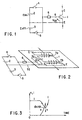
- FIG. 1 A conventional power converting apparatus using a MOS gate type semiconductor element having such a high withstand voltage will be described, with reference to FIGS. 1 to 3.
- a series circuit composed of a power supply 2 for applying a on-gate voltage Eon (usually +15V) and an on switch 4, and a series circuit composed of a power supply 3 for applying an off-gate voltage Eoff and an off switch 5 are connected between the gate and emitter of an IEGT 1 by a gate resistor 6 which serves for both on operation and off operation.
- the SECT 1 is turned on and a current flows through it when the switch 4 is closed, applying the on-gate voltage Eon on the gate and emitter of the IEGT 1 through the gate resistor 6.
- the switch 5 is closed, applying the off-gate voltage Eoff between the gate and emitter of the IEGT 1 through the gate resistor 6.
- the IEGT 1 is thereby turned off, cutting off the current.
- the IEGT 1 is connected to a collector terminal C by a plurality of collector wires 7a (four conductors as shown in the drawing), to an emitter E by a plurality of emitter wires 7b (four conductors as shown in the drawing), and to a gate terminal G by a gate wire 7c.
- Symbol 7d denotes an emitter wire for the gate.
- FIG. 3 shows the waveforms of the voltage and current applied and supplied to the IEGT 1 when the current is cut off in the circuit illustrated in FIG. 1.
- the voltage v applied to the IEGT 1 abruptly rises as the current i decreases.
- the voltage v may break the IEGT 1 down.
- a power converting apparatus comprises a MOS gate type semiconductor element section, an on-voltage applying section for applying an on-voltage between the gate and emitter terminals of the MOS gate type semiconductor element section, and an off-voltage applying section for applying an off-voltage between the gate and emitter terminals of the MOS gate type semiconductor element section.
- the apparatus is characterized by comprising an inductance element connected to the emitter terminal of the MOS gate type semiconductor element section.
- a power converting apparatus comprises a plurality of MOS gate type semiconductor elements, an on-voltage applying section for applying an on-voltage between the gate and emitter terminals of each MOS gate type semiconductor element, and an off-voltage applying section for applying an off-voltage between the gate and emitter terminals of each MOS gate type semiconductor element.
- the apparatus is characterized by further comprising a plurality of inductances connected to the emitter terminals of the MOS gate type semiconductor elements, respectively, and gate control means connected to the gate terminals of the MOS gate type semiconductor elements.
- an inductance element is inserted in the emitter terminals of the MOS gate type semi-conductor elements, and the emitter terminals for the gate is led from the position including this inductance.
- the voltage generated in the inductance from the cutoff voltage that flows at the time of turning off is used to mitigate the gate voltage. This mitigates dv/dt applied to the element, thereby preventing the breakdown of the element and improving the turn-off current balance between the chips of a multi-chip element.
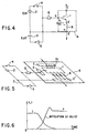
- the IEGT 1 and an emitter terminal E' are connected by inductance elements 8 in the present embodiment.
- the inductance element 8s are a plurality of coils (four coils are shown in the figures).
- di/dt becomes even greater when a large current is cut off, because the inductance elements 8 are inserted.
- the off gate voltage therefore decreases, mitigating dv/dt and preventing the breakdown of the element.
- the value of the voltage can be automatically corrected, thereby to prevent the breakdown of the element at the time of turn-off.
- a collector-side wire 7a is made shorter than the inductance elements 8 that serve also as emitter-side wires. This increases the ratio of the total length of the inductance elements 8 to the total length of all wires, assuming that the total length of all wires remains the same. The advantage of incorporating the inductance elements 8 into the module type element is thereby enhanced further.
- a maximum withstand voltage is applied to the gate of the IEGT.
- dielectric breakdown occurs.
- the gate withstand voltage of a MOS gate type semiconductor element should be suppressed to 100V or less.
- the cutoff current di/dt is usually 200A/ ⁇ s.
- the inductance L is set to have this value or a smaller value, the dielectric breakdown of the gate can be prevented.
- the gate voltage is about 15V.
- the voltage corrected by the inductance namely L*di/di, should be suppressed to 10V or less.
- What satisfies both 500 nH and 50 nH is 50 nH.
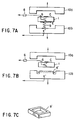
- the chip terminal E of the IEGT 1 and the terminal E' of the press-contact element are connected by an inductance element 9 shaped like a spring. Since the inductance element 9 is so connected to the emitter terminal, the increase in dv/dt, occurring at the time of turning off, can be mitigated to prevent the breakdown of the element.
- annular inductance element (reactor) 9' shown in FIG. 7C is used in place of the spring-shaped inductance element 9 used in the embodiment shown in FIG. 7A.
- the inductance element 9' is arranged, passing through the emitter-side terminal of the pressure-contact type element.
- a method of preventing the breakdown of an element, despite the increase in dv/dt, other than the use of the above-mentioned inductance element may be employed. This method is to increase the gate power-supply voltage gradually, not applying a high voltage.
- a CT (Current Transformer) 11 is used in the present embodiment.
- the CT 11 is connected to a line led from the emitter terminal of an IEGT 1, for detecting the current.
- a power amplifier 15 for receiving the output of the CT 11 and the outputs of resistors 12 to 14 is incorporated in the series circuit composed of an off switch 5 and a power supply 3 that applies an off-gate voltage Eoff.
- a circuit is connected to a gate terminal G and an emitter terminal E; it is provided, replacing the series circuit which is shown in FIG. 4 and which comprises the power supply 3 for applying the off-gate voltage Eoff and the off switch 5.
- the circuit comprises two series circuits.
- the first series circuit comprises a power supply 3a for applying an off-gate voltage Eoff and an off switch 5a.
- the second circuit comprises a power supply 3b for applying an off-gate voltage Eoff and an off switch 5g.
- the power supply 3a of the first series circuit applies, for example, -15V.
- the power supply 3b of the second series circuit applies -10V.
- the power supply of -15V is not used at first to apply the gate voltage, and the voltage of the power supply 5b of -10V is applied after the switch 5b has been closed to turn off the element.
- the switch 5b is opened to prevent erroneous turn-on of the IEGT 1.
- the switch 5a is closed, thereby applying -15 of the power supply 3a.
- a simple gate circuit can mitigate the vd/vt can be mitigated at the time of turning off.
- the fifth and sixth embodiments of this invention will be described, with reference to FIGS. 10A to 10C, FIGS. 11A to 11C, FIGS. 12A and 12B, and FIG. 13.
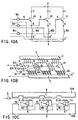
- the fifth embodiment shown in FIG. 10A has three IEGTs 1a, 1b and 1c connected in parallel.
- the emitter terminals E of the IEGTs 1a, 1b and 1c are connected to three module emitter E' by inductance elements 8a, 8b and 8c, respectively.
- Each of the inductance elements 8a, 8b and 8c comprises a plurality of coils (four coils, as shown in the figure).
- the gate voltage of the IEGT 1a changes to Eoff + L(di/dt). That is, the gate voltage for cutting off the current increases.
- the power (V GE +L*di/dt) for cutting off the current immediately increases even if the current starts concentrating.
- the power (V GE -L*di/dt) for cutting off the current decreases.
- the cutoff current of the IEGT 1a is therefore balanced with the cutoff current of the IEGT 1b and also with the cutoff current of the IEGT 1c.
- the IEGTs connected in parallel are balanced in terms of cutoff current in the present embodiment.
- the embodiment can, as a whole, can cut off a large current.
- this inductance element will improve not only the cutoff frequency ability of one IEGT, but also the balance of currents in the case where elements are connected in parallel. As a whole, the inductance element can serve to improve the cutoff frequency ability.
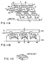
- FIG. 10B shows a plurality of IEGTs 1, which are wire-bonding type chips and incorporated in a module package.
- the bonding wires may be made short at the collector side and long at the emitter side. If so, the advantage of the present embodiment will be greater than otherwise.
- FIG. 10C shows a plurality of IEGTs 1, which are press-contact chips, connected in parallel and incorporated in a press-contact (planar) package.
- FIG. 11B shows another type of an apparatus, in which a plurality of IEGTs 1, or press-contact chips, are connected in parallel.
- Reactors 8' are cores.
- the emitter terminal E' has ends which project toward the IEGTs 1.
- the annular reactors 8' of the type shown in FIG. 11C are mounted around the projecting ends of the emitter E', practically providing the circuit illustrated in FIG. 11A.
- each IEGT becomes unbalanced at the time of turn-off, as is illustrated in FIG. 12A. In the present embodiment, it becomes better balanced as is depicted in FIG. 12B.
- a current sensor i.e., a resistor 100
- the resistor 100 detects an excessive current, causing a transistor 101 to lower the gate potential of the IEGT 1a, whereby the excessive current is suppressed. Gate-control protection is thus accomplished.
- the gate potentials of the chips come to differ during the protection. Consequently, the currents in the chips are likely to become unbalanced with one another.
- the currents in the chips can be balanced well because the reactors 8 control the gate voltages of the chips.
- di/dt greatly changes at the time of turn-off, depending on the value of the on-gate resistance.
- the change of di/dt is related to the time delay of the turn-off phenomenon, but the waveform of the voltage and the waveform of the current scarcely change at the time of turn-off.
- an IEGT In an element having a high withstand voltage, such as an IEGT, however, the current that can be cut off greatly changes with the value of the off-gate resistance.
- An IEGT has specific characteristics. As shown in FIG. 15A, the voltage and current change greatly and the switching loss is small if the off-gate resistance is low, but the current that can be cut off decreases. Conversely, if the off-gate resistance is high, the switching loss is large but the current that can be cut off can be large, as is illustrated in FIG. 15B.
- FIG. 16 shows an embodiment of the invention, in which a plurality of off-gate resistors are provided to make it possible to select a value for the current that can be cut off, from various values.
- This embodiment utilizes the above-mentioned characteristics of an IEGT in order to accomplish protection against a large current that may flow when the upper and lower arms of an inverter or the like are short-circuited.
- a CT 11 for detecting a fault current is connected to the line lead from the emitter terminal of an IEGT 1.
- the output of the CT 11 is supplied to a fault current determining circuit 18.
- Off switches 5a and 5b and resistors 17a and 17b are connected between the gate terminal of the IEGT 1 and a power supply 3 for applying off-gate voltage Eoff.
- the off switches 5a and 6b are controlled, either turned on or turned off, by the fault current determining circuit 18.
- the fault current determining circuit 18 usually closes the switch 5a, and the resistor 17a having a high resistance is thereby used as off-gate resistance.
- a large current such as a fault current can be safely cut off. Since a fault current is one that should not be cut off many times, it will not cause the breakdown of the element or affect the inverter loss even if the switching loss is large.
- This embodiment is different from the embodiment shown in FIGS. 10A to 10C or the embodiment shown in FIGS. 11A to 11C, in that six circuits of the type D (i.e., the circuit shown in FIG. 4) are connected, forming a bridge.
- the bridge circuit is connected between a dc capacitor 19 and a load 20, thereby constituting a three-phase inverter.
- the cut-off current of each IEGT increases, improving the current balance between the chips even more.
- the cut-off currents of MOS gate type semiconductor elements can be large.
- the embodiment can therefore be a power converting apparatus that has a large capacitance.
- This embodiment is a three-phase inverter. Nevertheless, it may be any other type of a power converting apparatus that uses MOS gate semiconductor elements, such as a pulse power supply, a dc power supply, a resonant power converting system, or a chopper circuit. Whichever power converting apparatus it may be, the present embodiment attains the same advantages.
- the present invention can provide a power converting apparatus in which neither an excessive dv/dt is applied to the elements at the time of turn-off, nor a current concentrates in some of the elements, the elements are therefore protected against breakdown, and a large current such as a fault current can be cut off.
Abstract
Description
Claims (18)
- A power converting apparatus comprising a MOS gate type semiconductor element section, an on-voltage applying section for applying an on-voltage between gate and emitter terminals of the MOS gate type semiconductor element section, and an off-voltage applying section for applying an off-voltage between the gate and emitter terminals of the MOS gate type semiconductor element section,said apparatus characterized by comprising an inductance element connected to the emitter terminal of the MOS gate type semiconductor element section.
- An apparatus according to claim 1, wherein the off-voltage applying section comprises means for applying different off-voltages between the gate and emitter terminals of the MOS gate type semiconductor element section.
- An apparatus according to claim 1, wherein the off-voltage applying section comprises:current detecting means for detecting a current flowing in the MOS gate type semiconductor element section; andmeans for applying a variable off-voltage to the MOS gate type semiconductor element section on the basis of a result detected by the current detecting means.
- An apparatus according to claim 1, further comprising:current detecting means for detecting a current flowing in the MOS gate type semiconductor element section;current determining means for determining a current value equal to or greater than a predetermined value, on the basis of a result detected by the current detecting means; andmeans for varying the gate resistance of the MOS gate type semiconductor element section on the basis of the result obtained by the current detecting means.
- An apparatus according to claim 1, characterized in that the inductance element has a value of 50n or less per element of the MOS gate type semi-conductor element section.
- An apparatus according to claim 1, characterized in that the MOS gate type semiconductor element section has a plurality of MOS gate type semiconductor elements, and the inductance element has a plurality of inductances.
- An apparatus according to claim 6, characterized in that the MOS gate type semiconductor element section comprises a plurality of MOS gate type semi-conductor elements connected in parallel.
- An apparatus according to claim 1, characterized in that the on-voltage applying section comprises:an on-voltage power supply for applying an on-voltage between the gate and emitter of the MOS gate type semiconductor element section; andswitching means connected between the gate terminal of the MOS gate type semiconductor element section and the on-voltage power supply.
- An apparatus according to claim 1, characterized in that the off-voltage applying section comprises:an off-voltage power supply for applying an off-voltage between the gate and emitter terminals of the MOS gate type semiconductor element section; andswitching means connected between the gate terminal of the MOS gate type semiconductor element section and the off-voltage power supply.
- An apparatus according to claim 1, characterized in that the inductance element is an annular reactor mounted on the emitter terminal of the MOS gate type semiconductor element section.
- A power converting apparatus comprising:a plurality of MOS gate type semiconductor elements;an on-voltage applying section for applying an on-voltage between gate and emitter terminals of each of said plurality of MOS gate type semiconductor elements; andan off-voltage applying section for applying an off-voltage between the gate and emitter terminals of each of said plurality of MOS gate type semiconductor elements,
characterized by comprising:a plurality of inductances connected to the emitter terminals of said plurality of MOS gate type semiconductor elements, respectively; andgate control means connected to the gate terminals of said plurality of MOS gate type semiconductor elements, for applying different gate voltages to the elements, respectively. - An apparatus according to claim 11, wherein the off-voltage applying section comprises means for applying a different off-voltage between the gate and emitter terminals of each of said MOS gate semi-conductor elements.
- An apparatus according to claim 11, wherein the off-voltage applying section comprises:current detecting means for detecting a current flowing in each of said plurality of MOS gate type semiconductor elements; andmeans for applying a variable off-voltage to the MOS gate type semiconductor elements on the basis of a result obtained by the current detecting means.
- An apparatus according to claim 1, further comprising:current detecting means for detecting currents flowing in said plurality of MOS gate type semi-conductor elements, respectively;current determining means for determining a current value equal to or greater than a predetermined value, on the basis of a result obtained by the current detecting means; andmeans for varying gate resistances of said plurality of MOS gate type semiconductor elements on the basis of the result obtained by the current detecting means.
- An apparatus according to claim 11, characterized in that each of the inductances has a value of 50n or less per element of the MOS gate type semi-conductor element section.
- An apparatus according to claim 11, characterized in that the on-voltage applying section comprises:an on-voltage power supply for applying an on-voltage between the gate and emitter of each of said plurality of MOS gate type semiconductor elements; andswitching means connected between the gate terminal of each of said plurality of MOS gate type semiconductor elements and the on-voltage power supply.
- An apparatus according to claim 11, characterized in that the off-voltage applying section comprises:an off-voltage power supply for applying an off-voltage between the gate and emitter terminals of each of said plurality of MOS gate type semiconductor elements; andswitching means connected between the gate terminal of each of said plurality of MOS gate type semiconductor elements and the off-voltage power supply.
- An apparatus according to claim 11, characterized in that each of the inductances is an annular reactor mounted on the emitter terminal of an associated one of said plurality of MOS gate type semiconductor elements.
Applications Claiming Priority (3)
| Application Number | Priority Date | Filing Date | Title |
|---|---|---|---|
| JP13318197 | 1997-05-23 | ||
| JP133181/97 | 1997-05-23 | ||
| PCT/JP1998/002267 WO1998053546A1 (en) | 1997-05-23 | 1998-05-22 | Power converter wherein mos gate semiconductor device is used |
Publications (3)
| Publication Number | Publication Date |
|---|---|
| EP0920114A1 true EP0920114A1 (en) | 1999-06-02 |
| EP0920114A4 EP0920114A4 (en) | 2005-05-04 |
| EP0920114B1 EP0920114B1 (en) | 2010-02-17 |
Family
ID=15098587
Family Applications (1)
| Application Number | Title | Priority Date | Filing Date |
|---|---|---|---|
| EP98921779A Expired - Lifetime EP0920114B1 (en) | 1997-05-23 | 1998-05-22 | Power converter wherein mos gate semiconductor device is used |
Country Status (5)
| Country | Link |
|---|---|
| EP (1) | EP0920114B1 (en) |
| JP (1) | JP3512426B2 (en) |
| CN (1) | CN1078971C (en) |
| DE (1) | DE69841505D1 (en) |
| WO (1) | WO1998053546A1 (en) |
Cited By (2)
| Publication number | Priority date | Publication date | Assignee | Title |
|---|---|---|---|---|
| EP0978942A2 (en) * | 1998-08-05 | 2000-02-09 | Kabushiki Kaisha Toshiba | Gate circuit |
| US10439606B2 (en) | 2017-08-15 | 2019-10-08 | Fuji Electric Co., Ltd. | Semiconductor module |
Families Citing this family (3)
| Publication number | Priority date | Publication date | Assignee | Title |
|---|---|---|---|---|
| JP3950836B2 (en) * | 2003-10-16 | 2007-08-01 | 株式会社東芝 | Vehicle control device |
| JP2012222932A (en) * | 2011-04-07 | 2012-11-12 | Mitsubishi Electric Corp | Switching device, and switching module |
| US10071634B2 (en) * | 2016-03-22 | 2018-09-11 | Ford Global Technologies, Llc | Dynamic IGBT gate drive to reduce switching loss |
Citations (3)
| Publication number | Priority date | Publication date | Assignee | Title |
|---|---|---|---|---|
| EP0420582A2 (en) * | 1989-09-29 | 1991-04-03 | Kabushiki Kaisha Toshiba | Drive circuit for a semiconductor device |
| US5204563A (en) * | 1992-01-22 | 1993-04-20 | Jason Barry L | Mosfet output circuit with improved protection method |
| EP0645889A1 (en) * | 1993-09-13 | 1995-03-29 | Siemens Aktiengesellschaft | Method and device for limiting the rate of current decrease at swith-off of semiconductor power switches with MOS control imput |
Family Cites Families (4)
| Publication number | Priority date | Publication date | Assignee | Title |
|---|---|---|---|---|
| JPH0246A (en) * | 1988-12-18 | 1990-01-05 | Ishida Katsutoshi | Information recording film |
| JP2621495B2 (en) * | 1989-08-02 | 1997-06-18 | 富士電機株式会社 | Gate drive circuit |
| JPH05336732A (en) * | 1992-06-02 | 1993-12-17 | Toshiba Corp | Igbt gate circuit |
| JPH07177727A (en) * | 1993-12-22 | 1995-07-14 | Toshiba Corp | Gate driving circuit and gate driving method of voltage-driven switching element |
-
1998
- 1998-05-22 DE DE69841505T patent/DE69841505D1/en not_active Expired - Lifetime
- 1998-05-22 CN CN98800691A patent/CN1078971C/en not_active Expired - Fee Related
- 1998-05-22 WO PCT/JP1998/002267 patent/WO1998053546A1/en active Application Filing
- 1998-05-22 JP JP55024698A patent/JP3512426B2/en not_active Expired - Fee Related
- 1998-05-22 EP EP98921779A patent/EP0920114B1/en not_active Expired - Lifetime
Patent Citations (3)
| Publication number | Priority date | Publication date | Assignee | Title |
|---|---|---|---|---|
| EP0420582A2 (en) * | 1989-09-29 | 1991-04-03 | Kabushiki Kaisha Toshiba | Drive circuit for a semiconductor device |
| US5204563A (en) * | 1992-01-22 | 1993-04-20 | Jason Barry L | Mosfet output circuit with improved protection method |
| EP0645889A1 (en) * | 1993-09-13 | 1995-03-29 | Siemens Aktiengesellschaft | Method and device for limiting the rate of current decrease at swith-off of semiconductor power switches with MOS control imput |
Non-Patent Citations (1)
| Title |
|---|
| See also references of WO9853546A1 * |
Cited By (3)
| Publication number | Priority date | Publication date | Assignee | Title |
|---|---|---|---|---|
| EP0978942A2 (en) * | 1998-08-05 | 2000-02-09 | Kabushiki Kaisha Toshiba | Gate circuit |
| EP0978942A3 (en) * | 1998-08-05 | 2003-10-01 | Kabushiki Kaisha Toshiba | Gate circuit |
| US10439606B2 (en) | 2017-08-15 | 2019-10-08 | Fuji Electric Co., Ltd. | Semiconductor module |
Also Published As
| Publication number | Publication date |
|---|---|
| CN1227011A (en) | 1999-08-25 |
| JP3512426B2 (en) | 2004-03-29 |
| WO1998053546A1 (en) | 1998-11-26 |
| EP0920114A4 (en) | 2005-05-04 |
| EP0920114B1 (en) | 2010-02-17 |
| DE69841505D1 (en) | 2010-04-01 |
| CN1078971C (en) | 2002-02-06 |
Similar Documents
| Publication | Publication Date | Title |
|---|---|---|
| JP3598933B2 (en) | Power converter | |
| US8213146B2 (en) | Semiconductor power conversion apparatus | |
| US5123746A (en) | Bridge type power converter with improved efficiency | |
| US5929665A (en) | Power converter with voltage drive switching device monitored by device parameters and electric parameters | |
| US5091664A (en) | Insulated gate bipolar transistor circuit with overcurrent protection | |
| JP4432215B2 (en) | Semiconductor switching element gate drive circuit | |
| EP0599455A2 (en) | Power transistor overcurrent protection circuit | |
| US20140184303A1 (en) | Power semiconductor device | |
| JP5925364B2 (en) | Power semiconductor device | |
| JP2019165542A (en) | Semiconductor device | |
| CN113497610A (en) | Gate drive circuit capable of reducing conduction loss of power semiconductor | |
| CN111030431B (en) | Semiconductor device with a semiconductor device having a plurality of semiconductor chips | |
| JPH0653795A (en) | Semiconductor device | |
| US6727516B2 (en) | Semiconductor power conversion apparatus | |
| EP0920114B1 (en) | Power converter wherein mos gate semiconductor device is used | |
| US5945868A (en) | Power semiconductor device and method for increasing turn-on time of the power semiconductor device | |
| JP6847641B2 (en) | Gate drive circuit | |
| JP3710439B2 (en) | Power module gate drive circuit | |
| JPH03183209A (en) | Drive circuit for voltage driven type semiconductor element | |
| JPH11234103A (en) | Method and device to control switching operation in power transistor | |
| JPH06105448A (en) | Switch device with protecting function | |
| US20120256493A1 (en) | Switching device and switching module | |
| WO2019054078A1 (en) | Power module, reverse-conducting igbt, and drive circuit | |
| JPH09130217A (en) | Semiconductor device | |
| JP6312946B1 (en) | Power semiconductor element drive circuit and motor drive device |
Legal Events
| Date | Code | Title | Description |
|---|---|---|---|
| PUAI | Public reference made under article 153(3) epc to a published international application that has entered the european phase |
Free format text: ORIGINAL CODE: 0009012 |
|
| 17P | Request for examination filed |
Effective date: 19990104 |
|
| AK | Designated contracting states |
Kind code of ref document: A1 Designated state(s): DE SE |
|
| A4 | Supplementary search report drawn up and despatched |
Effective date: 20050322 |
|
| 17Q | First examination report despatched |
Effective date: 20060329 |
|
| 17Q | First examination report despatched |
Effective date: 20060329 |
|
| GRAP | Despatch of communication of intention to grant a patent |
Free format text: ORIGINAL CODE: EPIDOSNIGR1 |
|
| GRAC | Information related to communication of intention to grant a patent modified |
Free format text: ORIGINAL CODE: EPIDOSCIGR1 |
|
| GRAS | Grant fee paid |
Free format text: ORIGINAL CODE: EPIDOSNIGR3 |
|
| GRAA | (expected) grant |
Free format text: ORIGINAL CODE: 0009210 |
|
| AK | Designated contracting states |
Kind code of ref document: B1 Designated state(s): DE SE |
|
| REF | Corresponds to: |
Ref document number: 69841505 Country of ref document: DE Date of ref document: 20100401 Kind code of ref document: P |
|
| REG | Reference to a national code |
Ref country code: SE Ref legal event code: TRGR |
|
| PLBE | No opposition filed within time limit |
Free format text: ORIGINAL CODE: 0009261 |
|
| STAA | Information on the status of an ep patent application or granted ep patent |
Free format text: STATUS: NO OPPOSITION FILED WITHIN TIME LIMIT |
|
| 26N | No opposition filed |
Effective date: 20101118 |
|
| PGFP | Annual fee paid to national office [announced via postgrant information from national office to epo] |
Ref country code: DE Payment date: 20170516 Year of fee payment: 20 |
|
| PGFP | Annual fee paid to national office [announced via postgrant information from national office to epo] |
Ref country code: SE Payment date: 20170511 Year of fee payment: 20 |
|
| REG | Reference to a national code |
Ref country code: DE Ref legal event code: R071 Ref document number: 69841505 Country of ref document: DE |
|
| REG | Reference to a national code |
Ref country code: SE Ref legal event code: EUG |