EP0925837A2 - Power processor circuit and method for corona discharge pollutant destruction apparatus - Google Patents
Power processor circuit and method for corona discharge pollutant destruction apparatus Download PDFInfo
- Publication number
- EP0925837A2 EP0925837A2 EP99200945A EP99200945A EP0925837A2 EP 0925837 A2 EP0925837 A2 EP 0925837A2 EP 99200945 A EP99200945 A EP 99200945A EP 99200945 A EP99200945 A EP 99200945A EP 0925837 A2 EP0925837 A2 EP 0925837A2
- Authority
- EP
- European Patent Office
- Prior art keywords
- corona discharge
- voltage
- pulses
- fets
- circuit
- Prior art date
- Legal status (The legal status is an assumption and is not a legal conclusion. Google has not performed a legal analysis and makes no representation as to the accuracy of the status listed.)
- Withdrawn
Links
Images


Classifications
-
- B—PERFORMING OPERATIONS; TRANSPORTING
- B03—SEPARATION OF SOLID MATERIALS USING LIQUIDS OR USING PNEUMATIC TABLES OR JIGS; MAGNETIC OR ELECTROSTATIC SEPARATION OF SOLID MATERIALS FROM SOLID MATERIALS OR FLUIDS; SEPARATION BY HIGH-VOLTAGE ELECTRIC FIELDS
- B03C—MAGNETIC OR ELECTROSTATIC SEPARATION OF SOLID MATERIALS FROM SOLID MATERIALS OR FLUIDS; SEPARATION BY HIGH-VOLTAGE ELECTRIC FIELDS
- B03C3/00—Separating dispersed particles from gases or vapour, e.g. air, by electrostatic effect
- B03C3/34—Constructional details or accessories or operation thereof
- B03C3/66—Applications of electricity supply techniques
- B03C3/68—Control systems therefor
-
- H—ELECTRICITY
- H01—ELECTRIC ELEMENTS
- H01T—SPARK GAPS; OVERVOLTAGE ARRESTERS USING SPARK GAPS; SPARKING PLUGS; CORONA DEVICES; GENERATING IONS TO BE INTRODUCED INTO NON-ENCLOSED GASES
- H01T19/00—Devices providing for corona discharge
-
- B—PERFORMING OPERATIONS; TRANSPORTING
- B01—PHYSICAL OR CHEMICAL PROCESSES OR APPARATUS IN GENERAL
- B01D—SEPARATION
- B01D53/00—Separation of gases or vapours; Recovering vapours of volatile solvents from gases; Chemical or biological purification of waste gases, e.g. engine exhaust gases, smoke, fumes, flue gases, aerosols
- B01D53/32—Separation of gases or vapours; Recovering vapours of volatile solvents from gases; Chemical or biological purification of waste gases, e.g. engine exhaust gases, smoke, fumes, flue gases, aerosols by electrical effects other than those provided for in group B01D61/00
-
- H—ELECTRICITY
- H02—GENERATION; CONVERSION OR DISTRIBUTION OF ELECTRIC POWER
- H02M—APPARATUS FOR CONVERSION BETWEEN AC AND AC, BETWEEN AC AND DC, OR BETWEEN DC AND DC, AND FOR USE WITH MAINS OR SIMILAR POWER SUPPLY SYSTEMS; CONVERSION OF DC OR AC INPUT POWER INTO SURGE OUTPUT POWER; CONTROL OR REGULATION THEREOF
- H02M7/00—Conversion of ac power input into dc power output; Conversion of dc power input into ac power output
- H02M7/42—Conversion of dc power input into ac power output without possibility of reversal
- H02M7/44—Conversion of dc power input into ac power output without possibility of reversal by static converters
- H02M7/48—Conversion of dc power input into ac power output without possibility of reversal by static converters using discharge tubes with control electrode or semiconductor devices with control electrode
- H02M7/53—Conversion of dc power input into ac power output without possibility of reversal by static converters using discharge tubes with control electrode or semiconductor devices with control electrode using devices of a triode or transistor type requiring continuous application of a control signal
- H02M7/537—Conversion of dc power input into ac power output without possibility of reversal by static converters using discharge tubes with control electrode or semiconductor devices with control electrode using devices of a triode or transistor type requiring continuous application of a control signal using semiconductor devices only, e.g. single switched pulse inverters
- H02M7/5387—Conversion of dc power input into ac power output without possibility of reversal by static converters using discharge tubes with control electrode or semiconductor devices with control electrode using devices of a triode or transistor type requiring continuous application of a control signal using semiconductor devices only, e.g. single switched pulse inverters in a bridge configuration
- H02M7/53871—Conversion of dc power input into ac power output without possibility of reversal by static converters using discharge tubes with control electrode or semiconductor devices with control electrode using devices of a triode or transistor type requiring continuous application of a control signal using semiconductor devices only, e.g. single switched pulse inverters in a bridge configuration with automatic control of output voltage or current
-
- Y—GENERAL TAGGING OF NEW TECHNOLOGICAL DEVELOPMENTS; GENERAL TAGGING OF CROSS-SECTIONAL TECHNOLOGIES SPANNING OVER SEVERAL SECTIONS OF THE IPC; TECHNICAL SUBJECTS COVERED BY FORMER USPC CROSS-REFERENCE ART COLLECTIONS [XRACs] AND DIGESTS
- Y02—TECHNOLOGIES OR APPLICATIONS FOR MITIGATION OR ADAPTATION AGAINST CLIMATE CHANGE
- Y02B—CLIMATE CHANGE MITIGATION TECHNOLOGIES RELATED TO BUILDINGS, e.g. HOUSING, HOUSE APPLIANCES OR RELATED END-USER APPLICATIONS
- Y02B70/00—Technologies for an efficient end-user side electric power management and consumption
- Y02B70/10—Technologies improving the efficiency by using switched-mode power supplies [SMPS], i.e. efficient power electronics conversion e.g. power factor correction or reduction of losses in power supplies or efficient standby modes
-
- Y—GENERAL TAGGING OF NEW TECHNOLOGICAL DEVELOPMENTS; GENERAL TAGGING OF CROSS-SECTIONAL TECHNOLOGIES SPANNING OVER SEVERAL SECTIONS OF THE IPC; TECHNICAL SUBJECTS COVERED BY FORMER USPC CROSS-REFERENCE ART COLLECTIONS [XRACs] AND DIGESTS
- Y10—TECHNICAL SUBJECTS COVERED BY FORMER USPC
- Y10S—TECHNICAL SUBJECTS COVERED BY FORMER USPC CROSS-REFERENCE ART COLLECTIONS [XRACs] AND DIGESTS
- Y10S422/00—Chemical apparatus and process disinfecting, deodorizing, preserving, or sterilizing
- Y10S422/907—Corona or glow discharge means
Definitions
- This invention relates to a power processor circuit and method for supplying power to generate corona discharge in a corona discharge pollutant destruction corona discharge reactor.
- a pollutant destruction system using an inductor-capacitor (LC) resonant circuit for corona discharge generation is described in EP-A-0744802, corresponding to USSN 08/450,449, filed May 25, 1995, "Gaseous Pollutant Destruction Apparatus and Method Using Self-Resonant Corona Discharge," and assigned to Hughes Aircraft Company, the assignee of the present invention.
- the application discloses a single stage corona discharge reactor driven by an LC resonator circuit, which is efficient in converting high-voltage pulse energy to corona discharges.
- High voltage pulses are very effective in destroying hydrocarbons (HC) and carbon monoxide (CO), but do not facilitate the reduction of nitrogen oxides (NO x ) into diatomic nitrogen (N 2 ) and oxygen (O 2 ).
- NO x nitrogen oxides
- N 2 diatomic nitrogen
- O 2 oxygen
- high voltages up to 12 kV
- low voltage pulses are highly efficient in reducing NO x , but are very poor at oxidizing HC. Therefore, depending on the treatment desired, a wide range of voltages levels and frequencies may be required.
- High voltage and high frequency electricity must be supplied to a corona discharge reactor to generate a corona discharge.
- the voltage required is usually in the range of about 5-20 kV, and the frequency required is usually in the range of about 5 to 15 MHz.
- a series resonant inverter with a feedback control loop for generating the required waveform is described in Patent No. 4,757,432. Spark gap circuits have been used for generating high voltage pulses for corona discharge, and are described in A. Mizuno et al., "NO x Removal Process Using Pulsed Discharge Plasma," IEEE Transactions on Industry Applications , vol. 31, 1995, pages 957-962, and T. Fujii et al., "Pulse Corona Characteristics,” IEEE Transactions on Industry Applications, vol. 29, 1993, pages 98-102.
- This invention concerns a power processor circuit for supplying power to generate a corona discharge in a corona discharge pollutant destruction reactor.
- Several embodiments of the invention utilize discrete solid state field effect transistor (FET) circuits or FET integrated circuits (ICs) to drive high voltage pulses by using direct current (DC) power supplies of only several hundred volts, thereby greatly reducing the volume, weight and cost of the circuits.
- FET solid state field effect transistor
- ICs FET integrated circuits
- a series resonant inductor-capacitor (LC) circuit is driven by four high power metal-oxide semiconductor field effect transistors (MOSFETs) operating with voltages and currents on the order of 1000 volts and 20 amperes and are connected in a "full bridge" configuration driven by a DC voltage on the order of 900 volts.
- the LC circuit resonates at about 5-15 MHz.
- the symmetrically arranged MOSFETs drive the LC resonator, with each MOSFET connected to a driver circuit that comprises multiple parallel stages of FETs.
- Each FET in the driver circuit is connected to at least one amplification and isolation circuit that receives rectangular pulses from a low-voltage signal source.
- the isolation circuits used in one embodiment are voltage transformers which isolate currents between the FETs and initial amplifiers.
- the driver circuit is also isolated from the signal source to protect the signal source from the driver circuit's high voltages and currents. Isolation may be achieved by a remote transmitter/receiver, such as a fiber optic transmitter/receiver link that transmits optical pulse signals from the signal source to the driver circuit but blocks voltages and currents.
- two high power MOSFETs are connected to only one end of a series LC resonator circuit in a "half bridge" configuration and are biased by DC voltages of only about ⁇ 200 volts.
- Each MOSFET is connected to a driver circuit comprising multiple parallel stages of high speed FET IC drivers capable of amplifying high frequency pulses.
- a low-voltage signal source transmits rectangular pulses to the driver circuits but is electrically isolated from them to avoid damage by high voltages and currents. Isolation may be achieved by a fiber optic transmitter/receiver link, for example, or by other remote transmitter/receiver means.
- no voltage transformers are needed, and in each parallel driver stage, only one high speed driver is connected between the fiber optic receiver and the high power MOSFET.
- the present invention concerns power processor circuits which employ discrete solid state field effect transistors (FETs) or FET integrated circuits (ICs) and relatively low DC voltages to generate high-voltage, high-frequency pulses for corona discharge generation.
- the circuits drive an LC resonator circuit for corona discharge generation by high power FET amplifiers in a power stage, with each high power FET amplifier driven by a driver circuit, which comprises discrete FETs and/or FET ICs, to feed amplified pulses at an intermediate voltage level to the power stage.
- the high power amplifier circuits are further provided with appropriate isolation circuits if necessary to prevent large voltages and currents in the high power circuits from damaging a low-voltage signal source, which provides a desired pulse waveform of preferably rectangular shape in the time domain.
- a low-voltage signal source which provides a desired pulse waveform of preferably rectangular shape in the time domain.
- One advantage of using rectangular pulses is that the duty cycle, which is defined as the ratio of pulse width to pulse repetition period, can be easily adjustable in the low-voltage signal source without changing any components or parameters in the high power circuits.
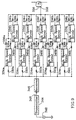
- the power stage shown in FIG. 1 comprises four high power FETs 2a, 2b, 2c, 2d having respective gates 4a, 4b, 4c, 4d, drains 6a, 6b, 6c, 6d and sources 8a, 8b, 8c, 8d.
- the high power FETs 2a, 2b, 2c, 2d are preferably n-channel transistors. It is further preferred that the FETs 2a, 2b, 2c, 2d be metal-oxide semiconductor FETs (MOSFETs) because of their ability to produce high power without breakdown when high voltages are applied to the gates.
- MOSFETs metal-oxide semiconductor FETs
- the high power FET gates 4a, 4b, 4c, 4d are connected to respective driver circuits 10a, 10b, 10c, 10d to amplify pulses from an intermediate voltage to a high voltage.
- An LC resonator circuit 12 is formed by an inductor 14 and a capacitor 16 connected in series, and the inductor 14 is connected in parallel with a corona discharge reactor 18.
- the inductor 14 preferably has an inductance of about 4.5 nH and the capacitor 16 preferably has a capacitance of about 25 pF.
- the inductor 14 and the capacitor 16 be connected in series to avoid breakdown at the capacitor.
- the four high power FETs 2a, 2b, 2c, 2d are arranged symmetrically about the resonator circuit 12 such that FETs 2a, 2b are connected to one end of the resonator circuit 12 while FETs 2c, 2d are connected to the other end.
- the FETs 2a, 2c have their drains 6a, 6c connected to a DC voltage source 20 which supplies a bias voltage V+, preferably of about +900 volts.
- a filter capacitor 22 is connected between the DC voltage source 20 and ground to filter out the DC component of an amplified voltage waveform in which the DC component is generated by the bias voltage V+, so that the DC source 20 is not short-circuited to ground.
- the sources 8a, 8c of the FETs 2a, 2c are connected to the drains 6b, 6d of the FETs 2b, 2d respectively, while the sources 8b, 8d of the FETs 2b, 2d are grounded.
- the resonator circuit 12 is connected across the sources 8a, 8c of the FETs 2a, 2c, thereby forming a full bridge circuit.
- a high power FET 40 which represents one of the FETs 2a, 2b, 2c, 2d, has a gate 42 that is connected to multiple parallel isolation-amplification stages 43a, 43b with intermediate n-channel FETs 44a, 44b, and to multiple parallel isolation-amplification stages 45a, 45b with intermediate p-channel FETs 46a, 46b to provide amplified intermediate-voltage pulses to the gate 42 of the high power FET 40.
- Resistors 48a, 48b, 50a, 50b of a small resistance, preferably in the range of 1 to 2 ⁇ , are added to drains 52a, 52b, 54a and 54b, respectively.
- the sources 56a, 56b of the n-channel FETs 44a, 44b are grounded, while the sources 58a, 58b of the p-channel FETs 46a, 46b are connected to a positive bias voltage +V 2 , preferably in the range of 12 to 15 V.
- Gates 60a, 60b of the n-channel FETs 44a, 44b are connected to the secondary coils of respective 1:1 turns ratio transformers 64a, 64b with the same polarization, while gates 62a, 62b of the p-channel FETs 46a, 46b are connected to the secondary coils of respective 1:1 turns ratio transformers 66a, 66b but with reverse polarization.
- Resistors 68a, 68b, 70a, 70b of a small resistance are, preferably connected between the transformers 64a, 64b, 66a, 66b and the gates 60a, 60b, 62a, 62b, respectively, to dampen possible ringing by the intermediate FETs 44a, 44b, 46a, 46b that could cause undesirable resonance interactions between them.
- the primary coils of the transformers 64a, 64b, 66a, 66b are connected to respective capacitors 72a, 72b, 74a, 74b to filter out DC components of pulses that are biased by a DC voltage.
- FIG. 2 shows two isolation-amplification stages with n-channel FETs and two stages with p-channel FETs, more stages of the same configuration may be added in parallel if desired to provide amplified pulse signals to the gate 42 of the high power FET 40.
- the inputs to all isolation-amplification stages with n-channel FETs are connected to a pair of npn bipolar transistors 76a, 76b, while the inputs to all isolation-amplification stages with p-channel FETs are connected to a pair of pnp bipolar transistors 78a, 78b.
- Collectors 80a, 82a of the npn transistors 76a, 78a are connected to a bias voltage +V 1 , which preferably has a positive DC voltage in the range of 12 to 15 V.
- Collectors 80b, 82b of the pnp transistors 76b, 78b are grounded.
- the emitters 84a, 86a of the npn transistors 76a, 78a are respectively connected to the emitters 84b, 86b of the pnp transistors 76b, 78b to form two nominally identical pairs of bipolar transistors, one pair for n-channel FET isolation-amplification stages and the other for p-channel FET isolation-amplification stages.
- the connected emitters 84a, 84b feed pulse signals to the n-channel FET stages, while the connected emitters 86a, 86b feed pulse signals to the p-channel FET stages.
- the bipolar transistor pairs form push-pull switching circuits which provide driving pulses to the isolationamplification stages.
- Bases 88a, 88b of the paired transistors 76a, 76b are connected to a high speed driver 92, and bases 90a, 90b of the paired transistors 78a, 78b are connected to another high speed driver 94.
- the high speed drivers 92, 94 are ICs that contain a plurality of solid state amplifier circuits capable of fast rise and fall times. They are preferably Elantec High Speed Drivers of the type "EL7104CN" MOSFET ICs.
- the drivers 92, 94 have respective input pairs 96, 98 and 100, 102, which may be connected directly to receive input pulse signals.
- diodes 112, 114 directed in opposite directions are respectively connected through resistors 104, 106 to the two inputs 96 and 98 of the driver 92.
- the resistors 104, 106 are preferably of a small resistance of 5 ⁇ or less.
- a pair of contra-directed diodes 116, 118 are preferably connected through respective resistors 108, 110 to feed input pulse signals to the inputs 100, 102 of the other driver 94.
- preamplifier circuits 101a, 101b The two pairs of bipolar transistors 76a, 76b and 78a, 78b and their associated drivers 92, 94 along with their pulse-shaping diodes and resistors form preamplifier circuits 101a, 101b, respectively. These preamplifier circuits are isolated from large currents in the intermediate FETs 44a, 44b, 46a, 46b by the transformers 64a, 64b, 66a, 66b.
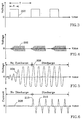
- a signal source 120 generates pulses 200 with a substantially rectangular waveform, as illustrated in FIG. 3.
- the rectangular pulses generally have a pulse width t and a pulse repetition period T.
- the duty cycle is defined as t/T, and the pulse repetition rate is defined as 1/T.
- the signal source 120 need only generate pulses of a low voltage level, on the order of 5 volts, for example.
- FIG. 2 shows the signal source 120 connected to a transmitter 122, which transmits the pulses to a receiver 124 via a communication link 126. In this configuration, the signal source 120 is isolated by the communication link 126 from the high voltages and currents in the driver circuits to enter the signal source 120 to prevent damaging the signal source.
- the transmitter 122 and the receiver 124 preferably use fiber optic transmission and reception schemes, and the link 126 is preferably a fiber optic cable which achieves a high level of electrical isolation between the signal source 120 and the remainder of the driver circuit.
- the transmitter/receiver isolation scheme is required for the driver circuits 10a, 10c in FIG. 1 because they operate at a high DC voltage V+, typically on the order of +900 volts.
- the signal source 120 may be connected directly to the diodes 112, 114, 116, 118 in the driver circuit without isolation.
- the rectangular pulses 200 in FIG. 3 are amplified by the driver circuits of FIG. 2 and the high power FET transistors 6a, 6b, 6c, 6d in the power stage circuit of FIG. 1.
- Each of the amplified rectangular pulses excites the LC resonator circuit 12, and causes it to "ring,” that is, to generate an oscillating high voltage wave at the resonant frequency of the circuit 12.
- power is continuously supplied to the resonator circuit 12, and forces the voltage amplitude of the resonant sinusoidal wave to increase rapidly to a saturation level.
- the peak voltage level remains substantially constant thereafter until the pulse is turned off.
- FIG. 4 shows a voltage waveform 202 across the corona discharge reactor 18 which results from the LC resonator circuit 12 being forced to resonate by the rectangular voltage pulses shown in FIG. 3.
- FIG. 5 shows the voltage waveform for one of the pulse periods of FIG. 4 expanded in the time domain, and illustrates the sinusoidal voltage 204 across the corona discharge reactor 18 generated by the forced resonance of a single pulse from the signal source 120. Initially, the amplitude of voltage 204 increases rapidly because of the ringing of the LC resonator circuit 12 forced by the pulse 200, but has not reached the voltage level necessary for corona discharge. There is no discharge within the corona discharge reactor chamber, and the current 208 across the reactor 18 is negligible, as shown in FIG. 6.
- the electrical characteristic of the corona discharge reactor during this period of no discharge may be represented by an equivalent circuit, shown in FIG. 7a, consisting of a single resistor 212 having a very high impedance.
- the corona discharge reactor may be regarded simply as an open circuit during the period of no discharge.
- the electrical characteristic of the corona discharge reactor 18 during discharge may be represented by an equivalent circuit consisting of a pair of Zener diodes 214, 216 connected in series but with opposite polarities as illustrated in FIG. 7b.
- an equivalent circuit consisting of a pair of Zener diodes 214, 216 connected in series but with opposite polarities as illustrated in FIG. 7b.
- FIG. 8 shows a preferred embodiment of a power stage circuit in a "half bridge" configuration. Only two high power FETs 300a, 300b are required, and DC bias voltages of only about ⁇ 200 V need to be provided.
- the high power FETs 300a, 300b are preferably n-channel and have gates 302a, 302b, drains 304a, 304b, and sources 306a, 306b, respectively. It is further preferred that the high power FETs 300a, 300b are MOSFETs of industry type "DE375X2 501N40.”
- the gates 302a, 302b of the FETs 300a, 300b are connected to respective driver circuits 308a, 308b, which provide initial amplification for the drive voltage pulses.
- the drain 304a of the first FET 300a is connected to a DC voltage source V+, which supplies a constant positive DC voltage V+ of preferably about +200 volts.
- a filter capacitor 314 is connected between V+ and ground to filter out the DC component of an amplified voltage waveform in which the DC component is generated by V+ to prevent V+ from short-circuiting to ground.
- the source 306b of the second FET 300b is connected to a negative DC voltage source V- of preferably about -200 volts.
- the source 306a of the first FET 300a and the drain 304b of the second FET 300b are connected together to form one node 322 of a resonator circuit 316, which preferably comprises an inductor 318 and a capacitor 320 connected in series.
- the opposite node 324 of the LC resonator circuit 316 is grounded.
- the inductor 318 is connected in parallel with a corona discharge reactor 18.
- the driver circuits 308a, 308b each have a configuration shown in FIG. 9 to amplify relatively low drive voltage pulses to an intermediate voltage level.
- a high power FET 330 which represents one of the FETs 300a, 300b in FIG. 8, has a gate 332 connected to the driver circuit, which comprises multiple high speed drivers 334a, 334b, ...334j connected in parallel with each other.
- the high speed drivers 334a, 334b, ...334j be MOSFET IC devices, preferably Elantec High Speed Drivers of the type "EL7104CN.” These high speed drivers 334a, 334b, ...334j each have two outputs connected to respective parallel resistors 336a, 336b, ...336j, 338a, 338b, ...338j of a low resistance, preferably on the order of 2.7 ⁇ . These resistors are connected to the gate 332 of the FET 330, so that amplified voltage pulses from the parallel high speed drivers 334a, 334b, ...334j are sent to the gate 332 of the high power FET 330 simultaneously.
- the high speed drivers 334a, 334b, ...334j also have respective inputs connected through respective input resistors 340a, 340b, ...340j to receive relatively low voltage pulse signals.
- pulses from signal source 342 are delivered by an optical transmitter 344 to an optical receiver 346 via a fiber optic cable 348.
- the receiver 346 is connected to the input resistors 340a, 340b, ...340j to send received pulse signals to the high speed drivers 334a, 334b, ...334j.
- the pulses generated by the signal source 342 are of a substantially rectangular shape in the time domain.
- the signal source 342 need only generate pulses at a low voltage level, on the order of 5 volts, for example. This isolation scheme is used for both driver circuits 308a, 308b in FIG. 8.
- a pair of discrete FETs are used in place of each of the high speed drivers 334a, 334b, ...334j of FIG. 9.
- a p-channel FET 250 and an n-channel FET 252 have gates 254, 256 connected to an input resistor 258 for receiving input pulse signals, and drains 260, 262 connected to respective output resistors 264, 266 for output to the power stage.
- the source 268 of the p-channel FET 250 is connected to a positive DC voltage +V 1 , while the source 270 of the n-channel FET 252 is grounded.
- the amplified rectangular pulses 200 of FIG. 3 force the LC resonator circuit 316 to resonate, thereby generating a voltage across the corona discharge reactor 18 with a wave pattern 202 generally shown in FIG. 4.
- the amplitude of the voltage wave 204 increases rapidly at the start of each pulse, as shown in FIG. 5, but is not high enough to generate a corona discharge.
- almost no current 208 passes through the corona discharge reactor 18 in the absence of a corona discharge.
- the voltage wave reaches a breakdown level 206 close to the peaks, corona discharges are generated and very large currents rapidly flow through the reactor 18, with each breakdown lasting a very short duration corresponding to the current spikes 210 in FIG. 6.
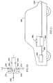
- FIG. 11 shows the implementation of a power processor circuit 382 in accordance with the invention in an automobile 390, which has an internal combustion engine 380 that generates a pollutant-bearing exhaust gas.
- the exhaust gas is transferred through an exhaust conduit 386 to a corona discharge reactor 384, which destroys the pollutants in the exhaust gas by corona discharge.
- the power processor circuit 382 supplies high voltage pulses to the reactor 384 to enable corona discharge generation.
- the treated exhaust gas exits the reactor through an outlet conduit 388.
- This invention provides a compact power source for corona discharge generation in automotive applications, and is particularly applicable to future electronic catalytic converters which employ corona discharge reactors to meet stringent air quality standards.
- the circuits embodied in this invention use only solid-state components, which would result in great savings in weight, cost and energy consumption, thereby making them suitable for automobile applications.
Abstract
Description
- This invention relates to a power processor circuit and method for supplying power to generate corona discharge in a corona discharge pollutant destruction corona discharge reactor.
- Passing a pollutant bearing gas through a corona discharge site is a known method of removing the pollutants from the gas. A general review of this technique is provided in Puchkarev et al., "Toxic Gas Decomposition by Surface Discharge," Proceedings of the 1994 International Conf. on Plasma Science, 6-8 June, 1994, Santa Fe, New Mexico, paper No. 1E6, page 88. Corona pollutant destruction has also been proposed for liquids, as disclosed in application Serial No. 08/295,959, filed August 25, 1994, "Corona Source for Producing Corona Discharge and Fluid Waste Treatment with Corona Discharge," and assigned to Hughes Aircraft Company, now doing business as Hughes Electronics.
- In one system, described in Yamamoto et al., "Decomposition of Volatile Organic Compounds by a Packed Bed Reactor and a Pulsed-Corona Plasma Reactor," Non-Thermal Plasma Techniques for Pollution Control, NATO ASI Series Vol. G34 Part B, Ed. by B.M. Penetrante and S.E. Schultheis, Springer-Verlag Berlin Heidelberg, 1993, pages 87-89, brief high voltage pulses of about 120-130 nanoseconds duration are applied to the center conductor of a coaxial corona reactor through which gas is flowing. Each pulse produces a corona discharge that emanates from the center wire and floods the inside volume of the reactor with energetic electrons at about 5-10 keV. A similar system is described in Patent No. 4,695,358, in which pulses of positive DC voltage are superimposed upon a DC bias voltage to generate a streamer corona for removing SOx and NOx from a gas stream. These processes have relatively poor energy efficiencies. With the reactor geometries that have been selected, it is necessary to deliver very short pulses to avoid arc breakdown between the electrodes, and consequent damage. The pulse-forming circuit loses approximately half of the power coming from a high voltage supply in a charging resistor, and additional energy is wasted in a double spark gap. Furthermore, the capacitive load of the coaxial corona reactor must be charged; this charging energy is typically much greater than the energy that is actually used in the corona reaction, and simply decays away into heat after each pulse without contributing to the pollutant destruction.
- A similar approach, but with a different reactor geometry, is taken in Rosocha et al., "Treatment of Hazardous Organic Wastes Using Silent-Discharge Plasmas," Non-Thermal Plasma Techniques for Pollution Control, NATO ASI Series Vol. G34 Part B, Ed. by B.M. Penetrante and S.E. Schultheis, Springer-Verlag Berlin Heidelberg, 1993, pages 79-80, in which the corona discharge is established between parallel plates. This system also suffers from a poor specific energy due to inefficient pulse formation and non-recovery of reactor charging energy.
- A pollutant destruction system using an inductor-capacitor (LC) resonant circuit for corona discharge generation is described in EP-A-0744802, corresponding to USSN 08/450,449, filed May 25, 1995, "Gaseous Pollutant Destruction Apparatus and Method Using Self-Resonant Corona Discharge," and assigned to Hughes Aircraft Company, the assignee of the present invention. The application discloses a single stage corona discharge reactor driven by an LC resonator circuit, which is efficient in converting high-voltage pulse energy to corona discharges. High voltage pulses are very effective in destroying hydrocarbons (HC) and carbon monoxide (CO), but do not facilitate the reduction of nitrogen oxides (NOx) into diatomic nitrogen (N2) and oxygen (O2). Experiments have shown that using high voltages (up to 12 kV) may even produce some additional NOx. On the other hand, low voltage pulses are highly efficient in reducing NOx, but are very poor at oxidizing HC. Therefore, depending on the treatment desired, a wide range of voltages levels and frequencies may be required.
- High voltage and high frequency electricity must be supplied to a corona discharge reactor to generate a corona discharge. The voltage required is usually in the range of about 5-20 kV, and the frequency required is usually in the range of about 5 to 15 MHz. A series resonant inverter with a feedback control loop for generating the required waveform is described in Patent No. 4,757,432. Spark gap circuits have been used for generating high voltage pulses for corona discharge, and are described in A. Mizuno et al., "NOx Removal Process Using Pulsed Discharge Plasma," IEEE Transactions on Industry Applications, vol. 31, 1995, pages 957-962, and T. Fujii et al., "Pulse Corona Characteristics," IEEE Transactions on Industry Applications, vol. 29, 1993, pages 98-102.
- This invention concerns a power processor circuit for supplying power to generate a corona discharge in a corona discharge pollutant destruction reactor. Several embodiments of the invention utilize discrete solid state field effect transistor (FET) circuits or FET integrated circuits (ICs) to drive high voltage pulses by using direct current (DC) power supplies of only several hundred volts, thereby greatly reducing the volume, weight and cost of the circuits.
- In one embodiment, a series resonant inductor-capacitor (LC) circuit is driven by four high power metal-oxide semiconductor field effect transistors (MOSFETs) operating with voltages and currents on the order of 1000 volts and 20 amperes and are connected in a "full bridge" configuration driven by a DC voltage on the order of 900 volts. The LC circuit resonates at about 5-15 MHz. The symmetrically arranged MOSFETs drive the LC resonator, with each MOSFET connected to a driver circuit that comprises multiple parallel stages of FETs. Each FET in the driver circuit is connected to at least one amplification and isolation circuit that receives rectangular pulses from a low-voltage signal source. The isolation circuits used in one embodiment are voltage transformers which isolate currents between the FETs and initial amplifiers. The driver circuit is also isolated from the signal source to protect the signal source from the driver circuit's high voltages and currents. Isolation may be achieved by a remote transmitter/receiver, such as a fiber optic transmitter/receiver link that transmits optical pulse signals from the signal source to the driver circuit but blocks voltages and currents.
- In another embodiment, two high power MOSFETs are connected to only one end of a series LC resonator circuit in a "half bridge" configuration and are biased by DC voltages of only about ±200 volts. Each MOSFET is connected to a driver circuit comprising multiple parallel stages of high speed FET IC drivers capable of amplifying high frequency pulses. A low-voltage signal source transmits rectangular pulses to the driver circuits but is electrically isolated from them to avoid damage by high voltages and currents. Isolation may be achieved by a fiber optic transmitter/receiver link, for example, or by other remote transmitter/receiver means. In this driver circuit, no voltage transformers are needed, and in each parallel driver stage, only one high speed driver is connected between the fiber optic receiver and the high power MOSFET.
- These and other features and advantages of the invention will be apparent to those skilled in the art from the following detailed description, taken together with the accompanying drawings, in which:
-
- FIG. 1 is a schematic diagram of the power stage for one embodiment of the invention that has a full bridge configuration;
- FIG. 2 is a schematic diagram of one of the driver circuits in the power processor circuit of FIG. 1;
- FIG. 3 is a plot of typical pulses provided to one of the driver circuits;
- FIG. 4 is a plot of typical exhaust gas chamber voltages, showing multiple pulses in the time domain;
- FIG. 5 is a plot on an expanded time scale of a portion of FIG. 4, showing sinusoidal waves energized by forced resonance within a single pulse;
- FIG. 6 is a plot of the typical current flowing across the exhaust gas chamber in the time domain;
- FIGs. 7a and 7b are equivalent circuits of a corona discharge reactor respectively without and during a discharge;
- FIG. 8 is a schematic diagram of the power stage for another embodiment in which the power processor circuit has a half bridge configuration;
- FIG. 9 is a schematic diagram of one of the driver circuits in the power processor circuit of FIG. 3, having a plurality of high speed drivers;
- FIG. 10 is a schematic diagram of an alternate embodiment for one of the high speed drivers used in FIG. 4; and
- FIG. 11 is a block diagram of an automobile that includes a power processor circuit in accordance with the invention that supplies power for corona discharge to treat engine exhaust gas.
-
- The present invention concerns power processor circuits which employ discrete solid state field effect transistors (FETs) or FET integrated circuits (ICs) and relatively low DC voltages to generate high-voltage, high-frequency pulses for corona discharge generation. The circuits drive an LC resonator circuit for corona discharge generation by high power FET amplifiers in a power stage, with each high power FET amplifier driven by a driver circuit, which comprises discrete FETs and/or FET ICs, to feed amplified pulses at an intermediate voltage level to the power stage. The high power amplifier circuits are further provided with appropriate isolation circuits if necessary to prevent large voltages and currents in the high power circuits from damaging a low-voltage signal source, which provides a desired pulse waveform of preferably rectangular shape in the time domain. One advantage of using rectangular pulses is that the duty cycle, which is defined as the ratio of pulse width to pulse repetition period, can be easily adjustable in the low-voltage signal source without changing any components or parameters in the high power circuits.
- In one embodiment employing a full bridge configuration, the power stage shown in FIG. 1 comprises four
high power FETs respective gates sources high power FETs FETs power FET gates respective driver circuits LC resonator circuit 12 is formed by aninductor 14 and acapacitor 16 connected in series, and theinductor 14 is connected in parallel with acorona discharge reactor 18. The resonant frequency f generated by theLC resonator circuit 12 is given byinductor 14 in henrys, C is the capacitance of thecapacitor 16 in farads, and f is the resonant frequency in hertz. To generate a desirable resonant frequency of about 15 MHz for optimal corona discharge, theinductor 14 preferably has an inductance of about 4.5 nH and thecapacitor 16 preferably has a capacitance of about 25 pF. Although other resonator configurations such as parallel LC resonator circuits are theoretically possible for generating a resonance, it is preferred that theinductor 14 and thecapacitor 16 be connected in series to avoid breakdown at the capacitor. - The four
high power FETs resonator circuit 12 such thatFETs resonator circuit 12 whileFETs FETs drains DC voltage source 20 which supplies a bias voltage V+, preferably of about +900 volts. Afilter capacitor 22 is connected between theDC voltage source 20 and ground to filter out the DC component of an amplified voltage waveform in which the DC component is generated by the bias voltage V+, so that theDC source 20 is not short-circuited to ground. Thesources FETs drains FETs sources FETs resonator circuit 12 is connected across thesources FETs - One embodiment of the
driver circuits high power FET 40, which represents one of theFETs gate 42 that is connected to multiple parallel isolation-amplification stages channel FETs amplification stages channel FETs gate 42 of thehigh power FET 40.Resistors drains sources 56a, 56b of the n-channel FETs channel FETs V. Gates channel FETs ratio transformers gates 62a, 62b of the p-channel FETs ratio transformers 66a, 66b but with reverse polarization.Resistors transformers gates intermediate FETs transformers respective capacitors gate 42 of thehigh power FET 40. - The inputs to all isolation-amplification stages with n-channel FETs are connected to a pair of npn
bipolar transistors 76a, 76b, while the inputs to all isolation-amplification stages with p-channel FETs are connected to a pair of pnpbipolar transistors Collectors 80a, 82a of thenpn transistors 76a, 78a are connected to a bias voltage +V1, which preferably has a positive DC voltage in the range of 12 to 15V. Collectors pnp transistors emitters npn transistors 76a, 78a are respectively connected to theemitters pnp transistors connected emitters connected emitters -
Bases transistors 76a, 76b are connected to ahigh speed driver 92, andbases 90a, 90b of the pairedtransistors high speed driver 94. Thehigh speed drivers drivers resistors inputs driver 92. Theresistors diodes respective resistors inputs other driver 94. The two pairs ofbipolar transistors drivers preamplifier circuits intermediate FETs transformers - A
signal source 120 generatespulses 200 with a substantially rectangular waveform, as illustrated in FIG. 3. The rectangular pulses generally have a pulse width t and a pulse repetition period T. The duty cycle is defined as t/T, and the pulse repetition rate is defined as 1/T. Thesignal source 120 need only generate pulses of a low voltage level, on the order of 5 volts, for example. FIG. 2 shows thesignal source 120 connected to atransmitter 122, which transmits the pulses to areceiver 124 via acommunication link 126. In this configuration, thesignal source 120 is isolated by thecommunication link 126 from the high voltages and currents in the driver circuits to enter thesignal source 120 to prevent damaging the signal source. Thetransmitter 122 and thereceiver 124 preferably use fiber optic transmission and reception schemes, and thelink 126 is preferably a fiber optic cable which achieves a high level of electrical isolation between thesignal source 120 and the remainder of the driver circuit. The transmitter/receiver isolation scheme is required for thedriver circuits driver circuits signal source 120 may be connected directly to thediodes - The
rectangular pulses 200 in FIG. 3 are amplified by the driver circuits of FIG. 2 and the highpower FET transistors LC resonator circuit 12, and causes it to "ring," that is, to generate an oscillating high voltage wave at the resonant frequency of thecircuit 12. During the pulse width t, power is continuously supplied to theresonator circuit 12, and forces the voltage amplitude of the resonant sinusoidal wave to increase rapidly to a saturation level. The peak voltage level remains substantially constant thereafter until the pulse is turned off. - FIG. 4 shows a
voltage waveform 202 across thecorona discharge reactor 18 which results from theLC resonator circuit 12 being forced to resonate by the rectangular voltage pulses shown in FIG. 3. FIG. 5 shows the voltage waveform for one of the pulse periods of FIG. 4 expanded in the time domain, and illustrates thesinusoidal voltage 204 across thecorona discharge reactor 18 generated by the forced resonance of a single pulse from thesignal source 120. Initially, the amplitude ofvoltage 204 increases rapidly because of the ringing of theLC resonator circuit 12 forced by thepulse 200, but has not reached the voltage level necessary for corona discharge. There is no discharge within the corona discharge reactor chamber, and the current 208 across thereactor 18 is negligible, as shown in FIG. 6. The electrical characteristic of the corona discharge reactor during this period of no discharge may be represented by an equivalent circuit, shown in FIG. 7a, consisting of asingle resistor 212 having a very high impedance. Alternatively, the corona discharge reactor may be regarded simply as an open circuit during the period of no discharge. When the voltage across thecorona discharge reactor 18 reaches acertain breakdown level 206, corona discharge occurs, and a large current flows across thereactor 18. Because the voltage reaches thebreakdown level 206 very close to the positive and negative peak of each sinusoidal lobe after the initial discharge, the current across thecorona discharge reactor 18 appears as positive andnegative spikes 210 because of the very short duration of each discharge. When the voltage falls below thebreakdown level 206, the current across thereactor 18 rapidly returns to a negligible level. - The electrical characteristic of the
corona discharge reactor 18 during discharge may be represented by an equivalent circuit consisting of a pair ofZener diodes diodes Zener diode pair - FIG. 8 shows a preferred embodiment of a power stage circuit in a "half bridge" configuration. Only two
high power FETs high power FETs gates sources high power FETs gates FETs respective driver circuits drain 304a of thefirst FET 300a is connected to a DC voltage source V+, which supplies a constant positive DC voltage V+ of preferably about +200 volts. Afilter capacitor 314 is connected between V+ and ground to filter out the DC component of an amplified voltage waveform in which the DC component is generated by V+ to prevent V+ from short-circuiting to ground. Thesource 306b of thesecond FET 300b is connected to a negative DC voltage source V- of preferably about -200 volts. Thesource 306a of thefirst FET 300a and thedrain 304b of thesecond FET 300b are connected together to form onenode 322 of aresonator circuit 316, which preferably comprises aninductor 318 and acapacitor 320 connected in series. Theopposite node 324 of theLC resonator circuit 316 is grounded. Theinductor 318 is connected in parallel with acorona discharge reactor 18. - In a preferred embodiment, the
driver circuits high power FET 330, which represents one of theFETs gate 332 connected to the driver circuit, which comprises multiplehigh speed drivers high speed drivers high speed drivers parallel resistors gate 332 of theFET 330, so that amplified voltage pulses from the parallelhigh speed drivers gate 332 of thehigh power FET 330 simultaneously. Thehigh speed drivers respective input resistors voltage signal source 342 from potential damage by high electrical power from the driver circuit, pulses fromsignal source 342 are delivered by anoptical transmitter 344 to anoptical receiver 346 via afiber optic cable 348. Thereceiver 346 is connected to theinput resistors high speed drivers signal source 342 are of a substantially rectangular shape in the time domain. Thesignal source 342 need only generate pulses at a low voltage level, on the order of 5 volts, for example. This isolation scheme is used for bothdriver circuits - In an alternate embodiment shown in FIG. 10, a pair of discrete FETs are used in place of each of the
high speed drivers channel FET 250 and an n-channel FET 252 havegates input resistor 258 for receiving input pulse signals, and drains 260, 262 connected torespective output resistors source 268 of the p-channel FET 250 is connected to a positive DC voltage +V1, while thesource 270 of the n-channel FET 252 is grounded. Although this circuit basically performs the equivalent functions of a high speed driver, it is more cumbersome to build and its operation is less reliable than thehigh speed drivers - In the preferred embodiment of the "half bridge" circuit of FIG. 8, the amplified
rectangular pulses 200 of FIG. 3 force theLC resonator circuit 316 to resonate, thereby generating a voltage across thecorona discharge reactor 18 with awave pattern 202 generally shown in FIG. 4. As in the embodiment of FIG. 1, the amplitude of thevoltage wave 204 increases rapidly at the start of each pulse, as shown in FIG. 5, but is not high enough to generate a corona discharge. As shown in FIG. 6, almost no current 208 passes through thecorona discharge reactor 18 in the absence of a corona discharge. When the voltage wave reaches abreakdown level 206 close to the peaks, corona discharges are generated and very large currents rapidly flow through thereactor 18, with each breakdown lasting a very short duration corresponding to thecurrent spikes 210 in FIG. 6. - FIG. 11 shows the implementation of a
power processor circuit 382 in accordance with the invention in anautomobile 390, which has aninternal combustion engine 380 that generates a pollutant-bearing exhaust gas. The exhaust gas is transferred through anexhaust conduit 386 to acorona discharge reactor 384, which destroys the pollutants in the exhaust gas by corona discharge. Thepower processor circuit 382 supplies high voltage pulses to thereactor 384 to enable corona discharge generation. The treated exhaust gas exits the reactor through anoutlet conduit 388. - This invention provides a compact power source for corona discharge generation in automotive applications, and is particularly applicable to future electronic catalytic converters which employ corona discharge reactors to meet stringent air quality standards. The circuits embodied in this invention use only solid-state components, which would result in great savings in weight, cost and energy consumption, thereby making them suitable for automobile applications.
- While several illustrative embodiments of the invention have been shown and described, numerous variations and alternate embodiments will occur to those skilled in the art. Such variations and alternate embodiments are contemplated, and can be made without departing from the spirit and scope of the invention as defined in the appended claims.
Claims (2)
- A method for converting relatively low voltage pulses to a relatively high voltage pulse modulated wave for corona discharge generation, comprising:amplifying said relatively low voltage pulses to generate high voltage pulses;forcing resonance by said high voltage pulses;generating said relatively high voltage pulse modulated wave from said forced resonance; andgenerating corona discharge by said relatively high voltage pulse modulated wave.
- The method of claim 1, wherein said low voltage pulses are initially amplified to generate intermediate voltage pulses, and said intermediate voltage pulses are further amplified to generate said high voltage pulses.
Applications Claiming Priority (3)
| Application Number | Priority Date | Filing Date | Title |
|---|---|---|---|
| US690000 | 1996-08-19 | ||
| US08/690,000 US5845488A (en) | 1996-08-19 | 1996-08-19 | Power processor circuit and method for corona discharge pollutant destruction apparatus |
| EP97306286A EP0825695A3 (en) | 1996-08-19 | 1997-08-19 | Power processor circuit and method for corona discharge pollutant destruction apparatus |
Related Parent Applications (1)
| Application Number | Title | Priority Date | Filing Date |
|---|---|---|---|
| EP97306286A Division EP0825695A3 (en) | 1996-08-19 | 1997-08-19 | Power processor circuit and method for corona discharge pollutant destruction apparatus |
Publications (2)
| Publication Number | Publication Date |
|---|---|
| EP0925837A2 true EP0925837A2 (en) | 1999-06-30 |
| EP0925837A3 EP0925837A3 (en) | 2000-07-12 |
Family
ID=24770699
Family Applications (2)
| Application Number | Title | Priority Date | Filing Date |
|---|---|---|---|
| EP99200945A Withdrawn EP0925837A3 (en) | 1996-08-19 | 1997-08-19 | Power processor circuit and method for corona discharge pollutant destruction apparatus |
| EP97306286A Withdrawn EP0825695A3 (en) | 1996-08-19 | 1997-08-19 | Power processor circuit and method for corona discharge pollutant destruction apparatus |
Family Applications After (1)
| Application Number | Title | Priority Date | Filing Date |
|---|---|---|---|
| EP97306286A Withdrawn EP0825695A3 (en) | 1996-08-19 | 1997-08-19 | Power processor circuit and method for corona discharge pollutant destruction apparatus |
Country Status (4)
| Country | Link |
|---|---|
| US (2) | US5845488A (en) |
| EP (2) | EP0925837A3 (en) |
| JP (1) | JP2948552B2 (en) |
| KR (1) | KR100242039B1 (en) |
Cited By (4)
| Publication number | Priority date | Publication date | Assignee | Title |
|---|---|---|---|---|
| WO2004112965A1 (en) * | 2003-06-25 | 2004-12-29 | Siemens Aktiengesellschaft | Electrostatic filter having a puncture detection function |
| AU2004205310B2 (en) * | 1999-10-14 | 2007-11-15 | Robert L Fuhriman Jr | High voltage power supply |
| WO2010054074A1 (en) | 2008-11-05 | 2010-05-14 | Fmc Technologies, Inc. | Electrostatic coalescer with resonance tracking circuit |
| CN103475244A (en) * | 2013-09-06 | 2013-12-25 | 西安电子科技大学 | Main circuit of single-phase inverter |
Families Citing this family (34)
| Publication number | Priority date | Publication date | Assignee | Title |
|---|---|---|---|---|
| US5863413A (en) | 1996-06-28 | 1999-01-26 | Litex, Inc. | Method for using hydroxyl radical to reduce pollutants in the exhaust gases from the combustion of a fuel |
| DE19626381C2 (en) * | 1996-07-01 | 1999-03-18 | Fraunhofer Ges Forschung | Method and device for low-pollution operation of an internal combustion engine |
| US5845488A (en) * | 1996-08-19 | 1998-12-08 | Raytheon Company | Power processor circuit and method for corona discharge pollutant destruction apparatus |
| US6029442A (en) | 1996-12-18 | 2000-02-29 | Litex, Inc. | Method and apparatus for using free radicals to reduce pollutants in the exhaust gases from the combustion of fuel |
| US6321531B1 (en) | 1996-12-18 | 2001-11-27 | Litex, Inc. | Method and apparatus for using free radicals to reduce pollutants in the exhaust gases from the combustion of a fuel |
| US6047543A (en) | 1996-12-18 | 2000-04-11 | Litex, Inc. | Method and apparatus for enhancing the rate and efficiency of gas phase reactions |
| CA2236769A1 (en) * | 1997-05-05 | 1998-11-05 | Ove K. Dunder | Ozone generator control system |
| US6461870B2 (en) * | 1998-05-06 | 2002-10-08 | Isotechnika Inc. | 13C glucose breath test for the diagnosis of diabetic indications and monitoring glycemic control |
| KR100448632B1 (en) * | 1998-12-21 | 2004-09-13 | 주식회사 포스코 | Apparatus and method for simutaneous removal of air pollutants using non-thermal plasma technology |
| GB9904069D0 (en) * | 1999-02-24 | 1999-04-14 | Aea Technology Plc | Dual voltage vehicle power supply system |
| KR100348408B1 (en) * | 1999-08-05 | 2002-08-10 | 주식회사제4기한국 | A device of dissolveing harmfull gas by using plasma |
| US6240692B1 (en) * | 2000-05-26 | 2001-06-05 | Louis L. Yost | Concrete form assembly |
| KR100344988B1 (en) * | 2000-06-27 | 2002-07-20 | 한국코트렐 주식회사 | Apparatus for forming electric discharge in a gas using high voltage impulse |
| US6432280B1 (en) | 2000-10-23 | 2002-08-13 | Pioneer Industrial Technologies, Inc. | Pollution control device |
| JP3595808B2 (en) | 2002-07-11 | 2004-12-02 | コニカミノルタホールディングス株式会社 | Voltage generating circuit and driving device provided with the circuit |
| US7254938B2 (en) * | 2003-12-16 | 2007-08-14 | Arvin Technologies, Inc. | Power supply and transformer |
| US6965722B1 (en) * | 2004-10-29 | 2005-11-15 | Finisar Corporation | High efficiency active matching electro-optic transducer driver circuit operable with low supply voltages |
| WO2006107390A2 (en) | 2005-04-04 | 2006-10-12 | Kronos Advanced Technologies, Inc. | An electrostatic fluid accelerator for and method of controlling a fluid flow |
| US20070137106A1 (en) * | 2005-12-19 | 2007-06-21 | Iverson Robert J | Method and apparatus for component control by fuel reformer operating frequency modulation |
| JP2007336618A (en) * | 2006-06-12 | 2007-12-27 | Pre-Tech Co Ltd | High-power circuit for high frequency |
| EP2297377B1 (en) | 2008-05-30 | 2017-12-27 | Colorado State University Research Foundation | Plasma-based chemical source device and method of use thereof |
| US8994270B2 (en) | 2008-05-30 | 2015-03-31 | Colorado State University Research Foundation | System and methods for plasma application |
| EP2299922B1 (en) | 2008-05-30 | 2016-11-09 | Colorado State University Research Foundation | Apparatus for generating plasma |
| WO2011123125A1 (en) | 2010-03-31 | 2011-10-06 | Colorado State University Research Foundation | Liquid-gas interface plasma device |
| US8222822B2 (en) | 2009-10-27 | 2012-07-17 | Tyco Healthcare Group Lp | Inductively-coupled plasma device |
| CA2794895A1 (en) | 2010-03-31 | 2011-10-06 | Colorado State University Research Foundation | Liquid-gas interface plasma device |
| US8760067B2 (en) * | 2011-04-04 | 2014-06-24 | Federal-Mogul Ignition Company | System and method for controlling arc formation in a corona discharge ignition system |
| US9532826B2 (en) | 2013-03-06 | 2017-01-03 | Covidien Lp | System and method for sinus surgery |
| US9555145B2 (en) | 2013-03-13 | 2017-01-31 | Covidien Lp | System and method for biofilm remediation |
| CN103825191B (en) * | 2014-03-21 | 2016-04-13 | 中国计量学院 | A kind of narrow spaces high peak power pulse formula semiconductor laser device driving circuit |
| WO2017147809A1 (en) * | 2016-03-02 | 2017-09-08 | 马骏 | Novel compressed air purification system having real-time monitoring function |
| CN107081046B (en) * | 2017-06-23 | 2023-10-17 | 杭州天明环保工程有限公司 | Pulse generating device for purifying flue gas |
| US11673007B2 (en) | 2020-12-24 | 2023-06-13 | Saied Tousi | Personal protective equipment that employs nanoparticles of two different metals that generate an electric field for inactivating microorganisms |
| US11471713B2 (en) * | 2020-12-24 | 2022-10-18 | Mohammad Taghi Fatehi | Personal protective equipment that employs an electric field for inactivating microorganisms |
Citations (5)
| Publication number | Priority date | Publication date | Assignee | Title |
|---|---|---|---|---|
| EP0034075A2 (en) * | 1980-01-24 | 1981-08-19 | Merlin Gerin | Static power supply device of an electrofilter for electrostatic dust precipitation |
| US4713220A (en) * | 1985-04-22 | 1987-12-15 | National Distillers And Chemical Corporation | Ozonator power supply |
| US4757432A (en) * | 1981-11-17 | 1988-07-12 | Hughes Aircraft Company | Series resonant inverter with integrating feedback control loop |
| EP0340006A2 (en) * | 1988-04-28 | 1989-11-02 | Matsushita Electric Industrial Co., Ltd. | Non-resonance AC power source apparatus |
| EP0595232A2 (en) * | 1992-10-26 | 1994-05-04 | Kasuga Denki, Incorporated | Controlling apparatus for high frequency high voltage power source |
Family Cites Families (13)
| Publication number | Priority date | Publication date | Assignee | Title |
|---|---|---|---|---|
| US3846637A (en) * | 1970-12-10 | 1974-11-05 | J Gettinger | Apparatus for eliminating noxious gases from the exhaust of an internal combustion engine |
| US3862043A (en) * | 1972-12-26 | 1975-01-21 | Haakenson Rose H | Pollution control |
| US3943407A (en) * | 1973-08-01 | 1976-03-09 | Scientific Enterprises, Inc. | Method and apparatus for producing increased quantities of ions and higher energy ions |
| US4002921A (en) * | 1974-03-29 | 1977-01-11 | Union Carbide Corporation | High frequency power supply |
| USRE30320E (en) * | 1975-03-13 | 1980-07-01 | Union Carbide Corporation | Corona reaction method and apparatus |
| DE3472867D1 (en) * | 1984-02-29 | 1988-08-25 | Ibm | Power switching circuit |
| US4945721A (en) * | 1988-04-14 | 1990-08-07 | Environmental Research International, Inc. | Electromagnetic converter for reduction of exhaust emissions |
| US5284556A (en) * | 1991-05-01 | 1994-02-08 | Plasmachines, Inc. | Exhaust treatment system and method |
| US5124905A (en) * | 1991-07-22 | 1992-06-23 | Emerson Electric Co. | Power supply with feedback circuit for limiting output voltage |
| US5366701A (en) * | 1991-11-01 | 1994-11-22 | Environmental Plasma Arc Technology, Inc. | Apparatus and method for reducing pollutants in effluent gas flow utilizing an ionizing and resonance means |
| US5278492A (en) * | 1992-01-15 | 1994-01-11 | Henkel Corporation | Controllable AC power supply for an ozonator |
| US5549795A (en) * | 1994-08-25 | 1996-08-27 | Hughes Aircraft Company | Corona source for producing corona discharge and fluid waste treatment with corona discharge |
| US5845488A (en) * | 1996-08-19 | 1998-12-08 | Raytheon Company | Power processor circuit and method for corona discharge pollutant destruction apparatus |
-
1996
- 1996-08-19 US US08/690,000 patent/US5845488A/en not_active Expired - Fee Related
-
1997
- 1997-08-19 KR KR1019970039282A patent/KR100242039B1/en not_active IP Right Cessation
- 1997-08-19 EP EP99200945A patent/EP0925837A3/en not_active Withdrawn
- 1997-08-19 JP JP9222844A patent/JP2948552B2/en not_active Expired - Fee Related
- 1997-08-19 EP EP97306286A patent/EP0825695A3/en not_active Withdrawn
-
1998
- 1998-02-26 US US09/031,109 patent/US6007682A/en not_active Expired - Fee Related
Patent Citations (5)
| Publication number | Priority date | Publication date | Assignee | Title |
|---|---|---|---|---|
| EP0034075A2 (en) * | 1980-01-24 | 1981-08-19 | Merlin Gerin | Static power supply device of an electrofilter for electrostatic dust precipitation |
| US4757432A (en) * | 1981-11-17 | 1988-07-12 | Hughes Aircraft Company | Series resonant inverter with integrating feedback control loop |
| US4713220A (en) * | 1985-04-22 | 1987-12-15 | National Distillers And Chemical Corporation | Ozonator power supply |
| EP0340006A2 (en) * | 1988-04-28 | 1989-11-02 | Matsushita Electric Industrial Co., Ltd. | Non-resonance AC power source apparatus |
| EP0595232A2 (en) * | 1992-10-26 | 1994-05-04 | Kasuga Denki, Incorporated | Controlling apparatus for high frequency high voltage power source |
Cited By (10)
| Publication number | Priority date | Publication date | Assignee | Title |
|---|---|---|---|---|
| AU2004205310B2 (en) * | 1999-10-14 | 2007-11-15 | Robert L Fuhriman Jr | High voltage power supply |
| WO2004112965A1 (en) * | 2003-06-25 | 2004-12-29 | Siemens Aktiengesellschaft | Electrostatic filter having a puncture detection function |
| WO2010054074A1 (en) | 2008-11-05 | 2010-05-14 | Fmc Technologies, Inc. | Electrostatic coalescer with resonance tracking circuit |
| WO2010054082A1 (en) * | 2008-11-05 | 2010-05-14 | Fmc Technologies, Inc. | Electrostatic coalescer with intermediate insulating member |
| CN102202795B (en) * | 2008-11-05 | 2015-08-19 | Fmc技术股份有限公司 | There is the electrostatic coalescer of syntonic follow circuit |
| AU2009313534B2 (en) * | 2008-11-05 | 2015-11-19 | Fmc Technologies, Inc. | Electrostatic coalescer with resonance tracking circuit |
| US9321055B2 (en) | 2008-11-05 | 2016-04-26 | Fmc Technologies, Inc. | Gas electrostatic coalescer |
| US9440241B2 (en) | 2008-11-05 | 2016-09-13 | Fmc Technologies, Inc. | Electrostatic coalescer with resonance tracking circuit |
| US9962712B2 (en) | 2008-11-05 | 2018-05-08 | Fmc Technologies, Inc. | Separating primarily gas process fluids in an electrostatic coalescer |
| CN103475244A (en) * | 2013-09-06 | 2013-12-25 | 西安电子科技大学 | Main circuit of single-phase inverter |
Also Published As
| Publication number | Publication date |
|---|---|
| JPH10216462A (en) | 1998-08-18 |
| EP0925837A3 (en) | 2000-07-12 |
| US5845488A (en) | 1998-12-08 |
| EP0825695A3 (en) | 1999-12-22 |
| JP2948552B2 (en) | 1999-09-13 |
| KR19980018756A (en) | 1998-06-05 |
| US6007682A (en) | 1999-12-28 |
| EP0825695A2 (en) | 1998-02-25 |
| KR100242039B1 (en) | 2000-02-01 |
Similar Documents
| Publication | Publication Date | Title |
|---|---|---|
| US6007682A (en) | Power processor circuit and method for corona discharge pollutant destruction apparatus | |
| US7353771B2 (en) | Method and apparatus of providing power to ignite and sustain a plasma in a reactive gas generator | |
| EP0744802B1 (en) | Gaseous pollutant destruction apparatus and method using self-resonant corona discharge | |
| US5542967A (en) | High voltage electrical apparatus for removing ecologically noxious substances from gases | |
| US5970706A (en) | Automatic control method for corona discharge pollutant destruction | |
| US5603893A (en) | Pollution treatment cells energized by short pulses | |
| KR100273993B1 (en) | FUEL INJECTION SYSTEM AND METHOD FOR TREATMENT OF NOx IN A CORONA DISCHARGE POLLUTANT DESTRUCTION APPARATUS | |
| JP3109664B2 (en) | Hazardous gas purifier | |
| US20010035698A1 (en) | Method and unit for driving piezoelectric transformer used for controlling luminance of cold-cathode tube | |
| KR100239598B1 (en) | Multi-stage gaseous pollutant destruction apparatus and method | |
| EP0825691B1 (en) | Multi-electrode corona discharge pollutant destruction apparatus and method | |
| JP2005222779A (en) | Plasma processing device | |
| EP0824952B1 (en) | NOx reduction method in corona discharge pollutant destruction apparatus | |
| US20040182832A1 (en) | Fast pulse nonthermal plasma reactor | |
| KR100998177B1 (en) | Apparatus for generating electromagnetic field of high frequency capable of adjusting a magnetic field intensity and frequency and apparatus for purification of water comprising the same | |
| US6156162A (en) | Power supply for dielectric barrier discharge plasma | |
| JP2004289886A (en) | Pulse power supply unit | |
| GB2287630A (en) | Apparatus and method for treatment of gas by ionization | |
| Chung et al. | MOSFET switched 20 kv, 500 a, 100 ns pulse generator with series connected pulse transformers | |
| JPH11276842A (en) | Gas purification apparatus | |
| KR200253453Y1 (en) | Pulse generator of high voltage adopting cascading method | |
| RU1780180C (en) | Key-pulse generator | |
| WO2005115610A1 (en) | Fast pulse nonthermal plasma reactor |
Legal Events
| Date | Code | Title | Description |
|---|---|---|---|
| PUAI | Public reference made under article 153(3) epc to a published international application that has entered the european phase |
Free format text: ORIGINAL CODE: 0009012 |
|
| AC | Divisional application: reference to earlier application |
Ref document number: 825695 Country of ref document: EP |
|
| AK | Designated contracting states |
Kind code of ref document: A2 Designated state(s): AT BE CH DE FI FR GB IT LI LU NL SE |
|
| PUAL | Search report despatched |
Free format text: ORIGINAL CODE: 0009013 |
|
| AK | Designated contracting states |
Kind code of ref document: A3 Designated state(s): AT BE CH DE FI FR GB IT LI LU NL SE |
|
| RIC1 | Information provided on ipc code assigned before grant |
Free format text: 7B 03C 3/68 A, 7H 02M 7/48 B |
|
| 17P | Request for examination filed |
Effective date: 20001218 |
|
| 17Q | First examination report despatched |
Effective date: 20010910 |
|
| STAA | Information on the status of an ep patent application or granted ep patent |
Free format text: STATUS: THE APPLICATION IS DEEMED TO BE WITHDRAWN |
|
| 18D | Application deemed to be withdrawn |
Effective date: 20030516 |
|
| RIC1 | Information provided on ipc code assigned before grant |
Ipc: 7H 02M 7/48 A |