EP0939937B1 - Electronic card - Google Patents
Electronic card Download PDFInfo
- Publication number
- EP0939937B1 EP0939937B1 EP97938323A EP97938323A EP0939937B1 EP 0939937 B1 EP0939937 B1 EP 0939937B1 EP 97938323 A EP97938323 A EP 97938323A EP 97938323 A EP97938323 A EP 97938323A EP 0939937 B1 EP0939937 B1 EP 0939937B1
- Authority
- EP
- European Patent Office
- Prior art keywords
- card
- shield
- tabs
- shields
- connector
- Prior art date
- Legal status (The legal status is an assumption and is not a legal conclusion. Google has not performed a legal analysis and makes no representation as to the accuracy of the status listed.)
- Expired - Lifetime
Links
Images


Classifications
-
- H—ELECTRICITY
- H05—ELECTRIC TECHNIQUES NOT OTHERWISE PROVIDED FOR
- H05K—PRINTED CIRCUITS; CASINGS OR CONSTRUCTIONAL DETAILS OF ELECTRIC APPARATUS; MANUFACTURE OF ASSEMBLAGES OF ELECTRICAL COMPONENTS
- H05K5/00—Casings, cabinets or drawers for electric apparatus
- H05K5/02—Details
- H05K5/0256—Details of interchangeable modules or receptacles therefor, e.g. cartridge mechanisms
- H05K5/026—Details of interchangeable modules or receptacles therefor, e.g. cartridge mechanisms having standardized interfaces
- H05K5/0265—Details of interchangeable modules or receptacles therefor, e.g. cartridge mechanisms having standardized interfaces of PCMCIA type
- H05K5/0269—Card housings therefor, e.g. covers, frames, PCB
-
- G—PHYSICS
- G06—COMPUTING; CALCULATING OR COUNTING
- G06K—GRAPHICAL DATA READING; PRESENTATION OF DATA; RECORD CARRIERS; HANDLING RECORD CARRIERS
- G06K19/00—Record carriers for use with machines and with at least a part designed to carry digital markings
- G06K19/06—Record carriers for use with machines and with at least a part designed to carry digital markings characterised by the kind of the digital marking, e.g. shape, nature, code
- G06K19/067—Record carriers with conductive marks, printed circuits or semiconductor circuit elements, e.g. credit or identity cards also with resonating or responding marks without active components
- G06K19/07—Record carriers with conductive marks, printed circuits or semiconductor circuit elements, e.g. credit or identity cards also with resonating or responding marks without active components with integrated circuit chips
- G06K19/077—Constructional details, e.g. mounting of circuits in the carrier
- G06K19/0772—Physical layout of the record carrier
- G06K19/07735—Physical layout of the record carrier the record carrier comprising means for protecting against electrostatic discharge
Definitions
- the present invention relates to electronic cards and more particularly to exterior shells for such cards.
- PCMCIA Personal Computer Memory Card International Association
- US 5,548,483 B discloses an electronic card comprising a printed circuit board assembly interposed between card shields having edges wherein tabs on the edges of one shield being provided that engage recesses on the edge of the other shield and each of said tabs comprises a member having an oblique projection which engages said other shield.
- the electronic card of the invention comprises a printed circuit board interposed between card shields having edges. Tabs on the edges of one shield engage recesses on the edge of the other shield. Adequate rigidity is thereby provided.
- a frame bar is interposed between the shields. Also included is an I/O connector grounded without a separate ground contact and shielded over its length.
- the PCB assembly consists of the metallized receptacle I/O connector 1 at one end and the 68 pos MTB (MICRO TRIBEAM TM ) receptacle connector 2 at the other end of the board.
- This connector 2 has the two coding keys 3 and 4 integrated to sides of the plastic housing, simultaneously an upstanding ridge 5 on the top and bottom of this housing.
- top and bottom surfaces are also located two recesses 6.
- the I/O receptacle is described in detail hereafter.
- the top and bottom card shields 7 and 8 are identical stampings of sheet metal eg. stainless steel. Over a substantial length of the shield, at one side are preferably periodically spaced, located upstanding tabs 9, and on the other side at same locations and periodicity appropriate recesses 10. In addition, at the front side 13 of a shield are located two fixation tabs 11, while at the rear side of each shield are extension portions 12 which are perpendicularly bent to be flush with in front of the metal shield of the connector plug opening of I/O connector 1. Such a perpendicular bend results in an improved aesthetics and also prevents an opening between I/O connector and shield and prevents what is known as a "smile" effect of the card while allowing for proper axial positioning of the PCB assembly.
- a perpendicular bend results in an improved aesthetics and also prevents an opening between I/O connector and shield and prevents what is known as a "smile" effect of the card while allowing for proper axial positioning of the PCB assembly.
- the I/O connector is shown in Figs. 5a and 5b in which it is shown that plastic is removed at ends of the top and bottom plastic walls 20 to allow the entry from the rear (PCB side) of two metal springs with legs 21 and 22 having inwardly projecting latches 23 and 24 and ends 25 and 26.
- the latches 23 and 24 contact the metal shield plug connector 18 of assembled I/O plug connector while the ends 25 and 26 are pressed on metal upper and lower shields 7 and 8 to complete the total ground connection of system.
- These two metal spring members are connected to the ground track on the PCB at two connector ends by rivets, as in initial design.
- FIGs. 6a - 6b another embodiment is shown in which one metal piece is inserted over for the top and bottom plastic walls of receptacle I/O connector.
- the advantage in this arrangement being not only, is one part needed, but that the metal shield extends over the total length of the connector while ensuring there is no potential drop between the two ground locations situated at connector ends.
- the inward projecting latches 23 and 24 face the central plastic insert 13 to finally connect with mating plug I/O shield 18.
- the outward latches 27 of the other side of the I/O connector contact the upper and lower shields 7 and 8, while the edges 25 and 26 are located also against the edges of the card shields.
- FIGs. 7-8 a further development of the I/O receptacle shield in combination with the substitute for ground contact 7 in initial design, is shown.
- the upper and shield portions are shown as two separate halfs, each with symmetrical segments of latch retaining openings 12 facing towards each other.
- This design alternative is not only present a metal plate with latch retaining openings, but also present at the rear end 28 of the receptacle I/O, besides the area needed for SMT legs of terminals, a metal wall over the remaining width of the card.
- This feature is more clearly evident in Fig. 4 showing the rear from the PCB side view of the receptacle I/O.
- This rear end 28 (Fig. 8) in this design when locked above a similar wall extending from lower shield portion, then affords a means for EMI/ESD shielding between the PCB electronics circuit I/O connector on this side of the card assembly.
- the PCB assembly includes the metallized receptacle I/O connector 101 at one end and the 68 pos MTB receptacle connector 102 at the other end of the board.
- This MTB connector 102 has the two coding keys 103 and 104 integrated to sides of the plastic housing, simultaneously an upstanding ridge 105 on the top and bottom of this housing.
- the I/O receptacle is described in detail hereafter.
- the top and bottom card shields 107 and 108 are sheet metal e.g. stainless steel. Over a substantial length of the shield, at one side are periodically located upstanding tabs 109, and on the other side at same locations and periodicity are appropriate recesses 110. In addition, at the front side 113 of a shield is located a fixation tab 111, and at the rear side of the shield are extension portions 112 which are perpendicularly bent to be flush with in front of the metal shield of the connector plug opening of I/O connector 101 in the final card assembly condition. Such a perpendicular bend results in an improved aesthetics of the card while allowing for proper longitudinal axial positioning of the PCB assembly.
- the tabs 109 cooperate with recess 110 along side and fixation tabs 111 cooperate with oppositely positioned recess 144 on the opposite side of the top shield through slot 100, to obtain a final card assembly.
- FIG. 9 -10 and 14 a further development of the I/O receptacle shield in combination with the substitute for ground contact 107 in initial design, is shown.
- the upper and shield portions are shown as two separate halfves each with symmetrical segments of latch retaining openings 112 facing towards each other.
- This design is not only present at a metal plate with latch retaining openings, but also present at the rear end 128 of the receptacle I/O, besides the area needed for SMT legs of terminals, a metal wall over the remaining width of the card.
- Fig. 11 and 12 shows modified forms of securing tabs wherein the tabs 109 comprise an upstanding arcuate section 130 having opposed rigid sides 131 and chamfers 132 from which a spring latch 133 extends downwardly and outwardly.
- the recesses 110 are formed in a ledge 134.
- the ends of the recesses 110 have edges 135 and 136 which are angled inwardly to points 138.
- the tab 133 engages the underside of ledges 134 in the recesses 110.
- the two card shields of this embodiment are preferably made from 0.2mm stainless steel and have a number of mechanical snap fit fasteners. After assembling the two shields to each other, these fasteners make the card surprisingly and unexpectantly rigid and stiff against bending and torsion. These fasteners also effect good electrical connection for grounding between the two card shields due to multiple contact points, and also because no intermediate load bearing surfaces are utilized the card is optimally shielded for EMI.
- These fasteners comprise a number of tabs 109 which engage recesses 110. It will be seen from the drawings (in parts at Figs. 15 and 16) that each of the tabs 109 and latch 133 are angled inwardly from the perpendicular plane, for example, by angle of (Fig.
- Each tab 109 comprises a spring section 132 integrated with a latch 133, which hooks in a latch 134 underneath the area of each recess 110.
- This latch 133 holds the two card shields from opening after assembly. During mating, the tab 109 will be subjected to elastic bending and torsion forces from the tip of latch 133 up both rigid sides.
- Each tab 109 includes also two rigid sides 131 which engage with some play in both ends of the recess 110.
- the total number of rigid sides 131 and recess ends give the mechanical connection between the two card shields a high shear strength, which results in a high stiffness against bending and torsion.
- the two card shields are identical and are hermaphodite, that is, each shield contains both male and female fastening elements.
- the chamfers 132 will first touch the leading edges 135 and 136 so that they will guide the tab 109 to the end position beyond points 138 and guarantee that the latch 133 will hook underneath edge 134.
- the points 138 function as latches to hold the tab in position in the recess and provide an audible "snap" that indicates proper latching.
- the relative dimensions of the chamfers 132 and ledges 135 and 136 are designed to absorb manufacturing (stamping) tolerances.
- the latch mechanism is designed in a way that there is an initial play between the latch and the ledge 134 in vertical direction, which is taken away by a second spring function of ends 137 of the ledge. As these ends have a bending angle less than 90°, these make first contact when assembling the two card shields and then these have to be pressed together a little before the latch 133 will be mated. After that the latch mechanism has no further play.
- the overall cumulative lengths of the spring like tabs will be at least 10% of the length of the shield and more preferably will be 50% of the length of the shield.
- Fig. 9 it will also be seen that there is a slot 106 at each end of the connector 102, which allows the tab 111 to pass through the connector to engage a recess 144 in the opposing card shield.
- a completely metal to metal contact so that it is not necessary to engage the plastic in the connector 102. More particularly, if only two card shields 107 and 108 are engaged without using the connector 101 and 102 the resulting card case is rigid.
- FIGs. 18 - 21 an embodiment is shown in which no I/O receptacle is employed. Otherwise this embodiment is generally the same as that described in Figs. 9 - 17. That is, it has identical tabs 245 which engage identical recesses 254, and it also has a space 240 for an MTB connector (not shown).
- the joining tabs and recesses of the rear are disposed to the side and there is centrally adjoining panels 241 and 242.
- FIGs. 22 - 24 another embodiment is shown which is similar to the foregoing embodiment except that it makes use of a single 15 position I/O connector 343.
- the tabs 309 and recesses 310 are the same as was described above.
- the connecting tabs and recesses 345 and 354 respectively are positioned outwardly adjacent the I/O connector on the front end of the card while tabs 311 and recess 344 cooperate with each other on the MTV connector side.
- FIG. 25 - 27 another embodiment is shown which makes use of two I/O connectors 446 and 447. Otherwise this embodiment is essentially the same as the ones described above. It will be noted that at the rear end of this card the tab and recess 448 are positioned between the I / O connectors and the rear side of the card.
- Figs. 28 - 29 it will be seen that the full metal corners of the embodiments described above are comprised of a folded metal wall shown generally at 549.
- Figs. 30 - 31 it we be noted that this curved corner may be produced from a blank having a medial protrusion 450 and lateral protrusions 451 and 452 which may be folded upwardly and inwardly in segments to produce the desired rounded effect.
- EMI EST shielding or similar full metal shielding without use of plastic or open air. This feature is also aesthetically advantageous since it has no sharp edges.
- means are provided to appropriately align the two end connectors (I/O and the MTB connector) with respect to the PCB before their fixation by a solder reflow process.
- this alignment should be achieved without the need of tight connector peg-to-board hole clearances. Removing this requirement for both or one (e.g. MTB side) PCMCIA case would suffice.
- the embodiment includes the incorporation of a plastic bar which is attached to one side edge of the metal card shield as shown in Fig. 33. Since the frame-bar's attachment along the longitudinal direction in the card shield is a key subject, forthcoming discussion and diagrams are related to the combination. The same frame-bar is utilized in the top and bottom shields.
- Fig. 34 shows two different views (in addition to a 360 rotation of second view with respect to the first) of one such frame-bar 601 having several upstanding lobes 602 and two longitudinally separated upstanding pegs 603 towards its middle portion, while several tapered recessed areas 604 are distributed over its length.
- Each lobe has one vertical face 605 and a tapered face 607; this vertical face of all lobes form one integral vertical face as at 605 extending over the length of the frame-bar 601.
- This protrusion is along a semicircular periphery 608 and 608', which both protrude from vertical face 605 in a space adjacent to the PCB edge.
- This protrusion towards the PCB is slightly different for these two pegs 603 and 603' due to a slight difference in their sizes and it faces the metal card shield edge 610.
- the user can locate such an assembly on a previously prepared combination of frame 201 with metal card 613.
- Fig. 49 (without an I/O connector), the pegs 603 and 603' allow for the fixation of this assembly, as discussed previously. Looking from the I/O to the MTB connector side, and assuming that the PCB and connector tails are transparent, results in Fig. 38. Different perspective views can be derived from Fig. 39.
- Fig. 40 shows another aspect of this design useful in "inverse" application of a card assembly. Due to the coding keys, such a card may be inserted only in one direction into the peripheral equipment. By inverted application (misuse), large longitudinal forces may be transmitted by the MTB connector to through the solder legs to the PCB 616. If the user continues to insert push the card from the I/O side, there may be a mechanical rupture to the solder joints on PCB, destroying the card. As evident in Fig. 40, the rear end 624 of the MTB connector in this design butts against the front of the frame 601. Since the latter is fixed in the case, such forces may be easily withstood by the edges of the PCB before force is transmitted to the solder connection.
- the current specification for PCMCIA cards is 60 Newton.
- the peg lobes 602 shown in this figure as a cross-section over the total width of one lobe of the frame-bar 601 enter from opposite shield sides and locate in appropriate recesses in the shield edges 610, the relative longitudinal movements between the two shields are immobilized. Again, this immobilization mechanism is distributed on several locations, on both sides of the PCMCIA card (in the length direction). Many other designs are prone to failure in this mode of loading. This, therefore, is a significant advantage of this design.
- the integration of the frame-bar gives a further enhancement of assembly robustness in addition to an extra safeguard (PCB alignment/positioning and fixation) to the electronic circuitry contained within the case.
Abstract
Description
- The present invention relates to electronic cards and more particularly to exterior shells for such cards.
- An electronic card according to the closest prior art document is known from US 5 536 905 A wherein a circuit board assembly is supported by frame bars of a frame interposed between card shields.
- Electronic cards are widely used, especially for adding capacity and/or functionality to personal computers. The Personal Computer Memory Card International Association (PCMCIA) has established standards for such cards, and has categorized them as type I, type II and type III cards.
- From US 5,497,297 B a frame and cover structure for integrated circuit cards is known where the covers are each fixed on the frame and not on each other. Therefore, if the frame consists of molded plastic material, the cover and frame structure has no shielding qualities because the frame is a source of leakage.
- US 5,548,483 B discloses an electronic card comprising a printed circuit board assembly interposed between card shields having edges wherein tabs on the edges of one shield being provided that engage recesses on the edge of the other shield and each of said tabs comprises a member having an oblique projection which engages said other shield.
- Previously cards have employed cover shields latched and/or adhesively fixed to an intermediate frame and covers laser welded or ultrasonically welded together. More recent cards employ metal shields that are directly fixed together, without a frame. However, there are difficulties experienced in having such structures maintain sufficient rigidity to withstand flexing, bending and tension forces which would be expected to be placed on it in the course of ordinary use.
- There is, therefore, a need for and it is an object of the present invention to provide an electronic card which avoids the above mentioned difficulties.
- This object is accomplished by an electronic card as claimed in claim 1. Dependent claims are directed on features of preferred embodiments of the invention.
- The electronic card of the invention comprises a printed circuit board interposed between card shields having edges. Tabs on the edges of one shield engage recesses on the edge of the other shield. Adequate rigidity is thereby provided. A frame bar is interposed between the shields. Also included is an I/O connector grounded without a separate ground contact and shielded over its length.
- The invention is further described with reference to the accompanying drawings in which:
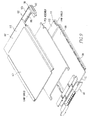
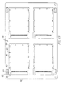
- Fig. 1 is an exploded perspective view of an electronic card;
- Fig. 2 is a perspective view of the card shown in Fig. 1;
- Fig. 3 is an enlarged view of the area in circle III in Fig. 1;
- Figs. 4a-4f are schematic illustrations of various ways in which the tabs and recesses in the card illustrated in Fig. 1 may be engaged within the scope of the present invention;
- Figs. 5a and 5b are respectively an exploded perspective view of an I/O connector used in the card shown in Fig. 1 and its accompanying universal grounding part and the I/O connector in which its universal grounding part is engaged;
- Figs. 6a and 6b are respectively an exploded view of an alternate I/O connector and a view of the alternate I/O connector in which its grounding part is engaged;
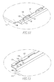
- Fig. 7 is an exploded perspective view of an alternate shielded I/O receptacle;
- Fig. 8 is a perspective view of an alternate shield member which may be used with the I/O receptacle shown in Fig. 7;
- Fig. 9 is an exploded perspective view of an alternate preferred embodiment of the card of the present invention;
- Fig. 10 is a bottom perspective view of the card of Fig. 9;
- Fig. 11 is a top perspective view of a card shield used in the card shown in Fig. 9;
- Fig. 12 is a detailed view of the area within circle XII in Fig. 11;
- Fig. 13 is a detailed view of the area with circle XIII in Fig. 11;
- Fig. 14 is a detailed view of the I/O connector used in the card connector shown in Fig. 9;
- Fig. 15 is a cross sectional view through an engaged latch;
- Fig. 16 is a cross section through XVII - XVII in Fig. 16; and
- Fig. 17 is a cross section through XVIII - XVIII in Fig. 16.
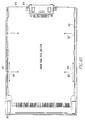
- Fig. 18 is a top plan view of a shield used in another preferred embodiment of the card of the present invention;
- Fig. 19 is a side elevational view of the shield shown in Fig. 18;
- Fig. 20 is an end view of the shield shown in Fig. 18;
- Fig. 21 is an end view of the entire card which makes use of the shield shown in Fig. 18;
- Fig. 22 is a top plan view of a shield used in another preferred embodiment of the card of the present invention;
- Fig. 23 is a side elevational view of the shield shown in Fig. 22;
- Fig. 24 is an end view of the shield shown in Fig. 22;
- Fig. 25 is a top plan view of a shield used in another preferred embodiment of the card of the present invention;
- Fig. 26 is a side elevational view of the shield shown in Fig. 22;
- Fig. 27 is an end view of the shield shown in Fig. 22;
- Fig. 28 is a partial perspective view of the shield shown in Fig. 18;
- Fig. 29 is an enlarged view of the area within circle XXIX in Fig. 28;
- Fig. 30 is a blank from which the shield shown in Fig. 18 may be manufactured;
- Fig. 31 is an enlarged view of the area within circle XXXI in Fig. 30;
- Figs. 32a and 32b are views of alternate preferred embodiments of tabs and recesses respectively.
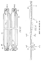
- Fig. 33 is a detailed perspective fragmented views of the frame bars used in the card of the present invention;
- Fig. 34 is a perspective view of the entire frame bar shown in Fig. 1;
- Figs. 35 - 38 are side and plan views of portions of the card;
- Figs. 39 - 42 are various perspective and schematic views illustrating the assembly of the frame in the shield;
- Figs. 43 - 46 are various plan and edge views illustrating various parts of the card;
- Figs. 47-51 are perspective illustrating various parts of the card;
- Fig. 52 is a side and top view of the frame support on the back of the coding key; and
- Fig. 53 is a schematic view illustrating a torque test of the card.
- Referring to Figs. 1-3, the PCB assembly consists of the metallized receptacle I/O connector 1 at one end and the 68 pos MTB (MICRO TRIBEAM™) receptacle connector 2 at the other end of the board. This connector 2 has the two coding keys 3 and 4 integrated to sides of the plastic housing, simultaneously an
upstanding ridge 5 on the top and bottom of this housing. On each of the two coding key ends of the connector 2, top and bottom surfaces, are also located two recesses 6. The I/O receptacle is described in detail hereafter. - The top and bottom card shields 7 and 8 are identical stampings of sheet metal eg. stainless steel. Over a substantial length of the shield, at one side are preferably periodically spaced, located
upstanding tabs 9, and on the other side at same locations and periodicityappropriate recesses 10. In addition, at thefront side 13 of a shield are located twofixation tabs 11, while at the rear side of each shield areextension portions 12 which are perpendicularly bent to be flush with in front of the metal shield of the connector plug opening of I/O connector 1. Such a perpendicular bend results in an improved aesthetics and also prevents an opening between I/O connector and shield and prevents what is known as a "smile" effect of the card while allowing for proper axial positioning of the PCB assembly. - When the two
card shield halves tabs 9 andfixation tabs 11 cooperate with oppositely positionedrecess 10 and 6 respectively, to obtain afinal card assembly 14 shown in Fig. 2. - Ordinarily if only one
tab 9 cooperates with one properly positionedrecess 10, the force to retain the card assembly structure intact (see Fig. 2), notwithstanding the mechanical flexure/tension it is subjected to during application, is low. Due, to the employment of a relatively large number of tabs and recesses evenly spaced over the assembly length on both sides, sufficient rigidity of the assembly can be achieved. In general, there can be, and usually is, a true-position mismatch-match between tabs and the recesses, due to stamping tolerances. As a result, there can be a friction-fit of the two card shields on each other and with the recesses 6 of plastic housing of MTB connector 2. These individual friction forces can be enhanced by appropriate choice of the relative dimension/shape of the tab/recess cooperating together to form the mechanical structure. For example, considering the Section A oftab 9 in Fig. 4a, frictional engagement between the tabs and recesses can result if the tab is longer than the recess, as shown in Fig. 4d, the tab is twisted (Fig. 4e) or the tab is curved (Fig. 4c). In addition, several options for latching the tab in the recess are presented in Fig. 4b and Fig. 4g and 4c and 4h, wherein a latch 9a, either centrally located or formed on one end of the tab, by a sheared portion, latches the tab in the recess when fully mated. The objective of the latching arrangements is to withstand the mechanical forces and hold the assembly intact. Another object is to present substantially flat metal sides of card assembly to allow appropriate contact with a ground contact of equipment slot (not shown) which the PCMCIA card needs to fit. - The I/O connector is shown in Figs. 5a and 5b in which it is shown that plastic is removed at ends of the top and bottom
plastic walls 20 to allow the entry from the rear (PCB side) of two metal springs withlegs latches latches lower shields - Referring to Figs. 6a - 6b, another embodiment is shown in which one metal piece is inserted over for the top and bottom plastic walls of receptacle I/O connector. The advantage in this arrangement, being not only, is one part needed, but that the metal shield extends over the total length of the connector while ensuring there is no potential drop between the two ground locations situated at connector ends. In this design, the inward projecting
latches central plastic insert 13 to finally connect with mating plug I/O shield 18. The outward latches 27 of the other side of the I/O connector contact the upper andlower shields edges - Referring to Figs. 7-8, a further development of the I/O receptacle shield in combination with the substitute for
ground contact 7 in initial design, is shown. Here the upper and shield portions are shown as two separate halfs, each with symmetrical segments oflatch retaining openings 12 facing towards each other. This design alternative is not only present a metal plate with latch retaining openings, but also present at therear end 28 of the receptacle I/O, besides the area needed for SMT legs of terminals, a metal wall over the remaining width of the card. This feature is more clearly evident in Fig. 4 showing the rear from the PCB side view of the receptacle I/O. This rear end 28 (Fig. 8) in this design when locked above a similar wall extending from lower shield portion, then affords a means for EMI/ESD shielding between the PCB electronics circuit I/O connector on this side of the card assembly. - Referring to Figs. 9-16, the PCB assembly includes the metallized receptacle I/
O connector 101 at one end and the 68 posMTB receptacle connector 102 at the other end of the board. ThisMTB connector 102 has the twocoding keys upstanding ridge 105 on the top and bottom of this housing. On each of the two coding key ends of theMTB connector 102, top and bottom surfaces, are also located on the I/O connector ends and tworecesses 106. The I/O receptacle is described in detail hereafter. - The top and bottom card shields 107 and 108 are sheet metal e.g. stainless steel. Over a substantial length of the shield, at one side are periodically located
upstanding tabs 109, and on the other side at same locations and periodicity areappropriate recesses 110. In addition, at thefront side 113 of a shield is located afixation tab 111, and at the rear side of the shield areextension portions 112 which are perpendicularly bent to be flush with in front of the metal shield of the connector plug opening of I/O connector 101 in the final card assembly condition. Such a perpendicular bend results in an improved aesthetics of the card while allowing for proper longitudinal axial positioning of the PCB assembly. - When the two card shield halves 107 and 108 are positioned and moved towards each to enclose of the PCB assembly, the
tabs 109 cooperate withrecess 110 along side andfixation tabs 111 cooperate with oppositely positionedrecess 144 on the opposite side of the top shield throughslot 100, to obtain a final card assembly. - The periodicity of tabs and recess over the assembly length on both sides, is sufficient to ensure the desired assembly rigidity. As previously stated, there usually is a true-position miss-match between the tabs and recess, due to stamping tolerances. This arrangement, then results in at least an initial friction-fit of the two card shields on each other by reason of the
side tabs 109 entering side recesses 110, and twofront fixation tabs 111 passing through two 106 to enterfront recess 144 of the opposite shield of plastic housing ofconnector 102. These individual friction forces can be enhanced by appropriate choice of the relative dimension/shape of the tab/recess cooperating together to form the mechanical structure. - Referring particularly to Figs. 9 -10 and 14, a further development of the I/O receptacle shield in combination with the substitute for
ground contact 107 in initial design, is shown. Here the upper and shield portions are shown as two separate halfves each with symmetrical segments oflatch retaining openings 112 facing towards each other. This design is not only present at a metal plate with latch retaining openings, but also present at therear end 128 of the receptacle I/O, besides the area needed for SMT legs of terminals, a metal wall over the remaining width of the card. - Fig. 11 and 12 shows modified forms of securing tabs wherein the
tabs 109 comprise an upstandingarcuate section 130 having opposedrigid sides 131 andchamfers 132 from which aspring latch 133 extends downwardly and outwardly. Referring particularly to Fig. 13, therecesses 110 are formed in aledge 134. The ends of therecesses 110 haveedges tab 133 engages the underside ofledges 134 in therecesses 110. - The two card shields of this embodiment are preferably made from 0.2mm stainless steel and have a number of mechanical snap fit fasteners. After assembling the two shields to each other, these fasteners make the card surprisingly and unexpectantly rigid and stiff against bending and torsion. These fasteners also effect good electrical connection for grounding between the two card shields due to multiple contact points, and also because no intermediate load bearing surfaces are utilized the card is optimally shielded for EMI. These fasteners comprise a number of
tabs 109 which engage recesses 110. It will be seen from the drawings (in parts at Figs. 15 and 16) that each of thetabs 109 and latch 133 are angled inwardly from the perpendicular plane, for example, by angle of (Fig. 15) to better engage therecesses 110. Eachtab 109 comprises aspring section 132 integrated with alatch 133, which hooks in alatch 134 underneath the area of eachrecess 110. Thislatch 133 holds the two card shields from opening after assembly. During mating, thetab 109 will be subjected to elastic bending and torsion forces from the tip oflatch 133 up both rigid sides. - Each
tab 109 includes also tworigid sides 131 which engage with some play in both ends of therecess 110. The total number ofrigid sides 131 and recess ends give the mechanical connection between the two card shields a high shear strength, which results in a high stiffness against bending and torsion. It will also be noted that the two card shields are identical and are hermaphodite, that is, each shield contains both male and female fastening elements. - As is shown in particular with regard to Figs. 12 - 14, during mating the
chamfers 132 will first touch the leadingedges tab 109 to the end position beyondpoints 138 and guarantee that thelatch 133 will hook underneathedge 134. Thepoints 138 function as latches to hold the tab in position in the recess and provide an audible "snap" that indicates proper latching. The relative dimensions of thechamfers 132 andledges - The latch mechanism is designed in a way that there is an initial play between the latch and the
ledge 134 in vertical direction, which is taken away by a second spring function ofends 137 of the ledge. As these ends have a bending angle less than 90°, these make first contact when assembling the two card shields and then these have to be pressed together a little before thelatch 133 will be mated. After that the latch mechanism has no further play. - Preferably the overall cumulative lengths of the spring like tabs will be at least 10% of the length of the shield and more preferably will be 50% of the length of the shield.
- Referring particularly to Fig. 9, it will also be seen that there is a
slot 106 at each end of theconnector 102, which allows thetab 111 to pass through the connector to engage arecess 144 in the opposing card shield. Thus there is a completely metal to metal contact so that it is not necessary to engage the plastic in theconnector 102. More particularly, if only twocard shields connector - A torque test, bend test and finger nail simulation test were conducted on this second PCMCIA card version described above. The tests are shown respectively on the attached Tables I, II and III.
- Referring to Figs. 18 - 21, an embodiment is shown in which no I/O receptacle is employed. Otherwise this embodiment is generally the same as that described in Figs. 9 - 17. That is, it has
identical tabs 245 which engageidentical recesses 254, and it also has aspace 240 for an MTB connector (not shown). Referring particularly to Figs. 20 - 21, it will be noted that the joining tabs and recesses of the rear are disposed to the side and there is centrally adjoiningpanels tabs 309 and recesses 310 are the same as was described above. In this embodiment the connecting tabs and recesses 345 and 354 respectively are positioned outwardly adjacent the I/O connector on the front end of the card while tabs 311 and recess 344 cooperate with each other on the MTV connector side. - Referring to Figs. 25 - 27, another embodiment is shown which makes use of two I/
O connectors recess 448 are positioned between the I / O connectors and the rear side of the card. - Referring to Figs. 28 - 29, it will be seen that the full metal corners of the embodiments described above are comprised of a folded metal wall shown generally at 549. Referring to Figs. 30 - 31, it we be noted that this curved corner may be produced from a blank having a
medial protrusion 450 andlateral protrusions - The following modifications may also be incorporated into the card described above.
- a) Incorporating a frame-bar in addition to the metal card shields to support the interior electronic circuitry; and
- b) Affording a means to mechanically connect and fix the metal card shields to the PCB.
- In this additional embodiment, means are provided to appropriately align the two end connectors (I/O and the MTB connector) with respect to the PCB before their fixation by a solder reflow process. Preferably this alignment should be achieved without the need of tight connector peg-to-board hole clearances. Removing this requirement for both or one (e.g. MTB side) PCMCIA case would suffice.
- To incorporate these changes a design modification has been undertaken without alteration to the basic metal latch snap-fit feature discussed earlier on edges of metal shield; neither is there a change to the basic I/O connector configuration.
- The embodiment includes the incorporation of a plastic bar which is attached to one side edge of the metal card shield as shown in Fig. 33. Since the frame-bar's attachment along the longitudinal direction in the card shield is a key subject, forthcoming discussion and diagrams are related to the combination. The same frame-bar is utilized in the top and bottom shields. Fig. 34 shows two different views (in addition to a 360 rotation of second view with respect to the first) of one such frame-
bar 601 having severalupstanding lobes 602 and two longitudinally separatedupstanding pegs 603 towards its middle portion, while several tapered recessedareas 604 are distributed over its length. Each lobe has onevertical face 605 and atapered face 607; this vertical face of all lobes form one integral vertical face as at 605 extending over the length of the frame-bar 601. The twopegs 603 and 603', each having a chamferedledge 606, protrude away from thevertical face 605. This protrusion is along asemicircular periphery 608 and 608', which both protrude fromvertical face 605 in a space adjacent to the PCB edge. This protrusion towards the PCB is slightly different for these twopegs 603 and 603' due to a slight difference in their sizes and it faces the metalcard shield edge 610. This is also the case for the tapered faces 607 as is further clear from Fig. 33 in whichcase 607 is opposite to the upstandingarcuate section 611 extending from themetal card 613 with several retaining latches 612 distributed over the length ofshield edge 610. - To understand the assembly of this frame-
bar 601 on one edge of onemetal card 613, the relative (process) positioning of theMTB connector 614 is effected by the use ofsteps 620 andtabs 619, using the concept of thepanel 618, is emphasized. Corresponding perspective versions are shown in Fig. 47 and 48. In these figures the connector rear ends 604 immediately behind the coding keys, are defined. Now the I/O connector 615 can be located inholes 623, shown in Fig. 44 still using the frame structure as positioning means. Once all other electronic circuitry elements have been located on the PCB by the customer, a single reflow operation is used to form an integral electronic assembly, for example, a PCMCIA card. This assembly obviously includes the two end connectors. Finally, each electronic assembly can be separated from the frame by shearing-off in the vicinity of thejoints 621. It is to be noted such a design foresees a means to accommodate also two I/O connectors, or no I/O connectors at all. - The user can locate such an assembly on a previously prepared combination of frame 201 with
metal card 613. As shown in Fig. 49 (without an I/O connector), thepegs 603 and 603' allow for the fixation of this assembly, as discussed previously. Looking from the I/O to the MTB connector side, and assuming that the PCB and connector tails are transparent, results in Fig. 38. Different perspective views can be derived from Fig. 39. - Fig. 40 shows another aspect of this design useful in "inverse" application of a card assembly. Due to the coding keys, such a card may be inserted only in one direction into the peripheral equipment. By inverted application (misuse), large longitudinal forces may be transmitted by the MTB connector to through the solder legs to the
PCB 616. If the user continues to insert push the card from the I/O side, there may be a mechanical rupture to the solder joints on PCB, destroying the card. As evident in Fig. 40, therear end 624 of the MTB connector in this design butts against the front of theframe 601. Since the latter is fixed in the case, such forces may be easily withstood by the edges of the PCB before force is transmitted to the solder connection. The current specification for PCMCIA cards is 60 Newton. - Another advantage of this design is its ability to withstand torque and twist, as demonstrated in Fig. 41. It needs to be understood that in this mode of mechanical loading, the upper and lower metal card constituting the PCMCIA assembly, have a tendency to move in opposite directions relative to each other. As the twist is being applied from the I/O end, the ensuing relative movement between the shields are effective at the MTB connector side. Consequently, the connection between the two card shields to the MTB connector ends, are subject to relatively large (shear) forces, which may easily rupture the joint. Since the
peg lobes 602, shown in this figure as a cross-section over the total width of one lobe of the frame-bar 601, enter from opposite shield sides and locate in appropriate recesses in the shield edges 610, the relative longitudinal movements between the two shields are immobilized. Again, this immobilization mechanism is distributed on several locations, on both sides of the PCMCIA card (in the length direction). Many other designs are prone to failure in this mode of loading. This, therefore, is a significant advantage of this design. Thus the integration of the frame-bar gives a further enhancement of assembly robustness in addition to an extra safeguard (PCB alignment/positioning and fixation) to the electronic circuitry contained within the case. - It will be appreciated that a card connector has been provided which allows for optimum shear strength and stiffness against bending and torsion.
- While the present invention has been described in connection with the preferred embodiments of the various figures, it is to be understood that other similar embodiments may be used or modifications and additions may be made to the described embodiment for performing the same function of the present invention without deviating therefrom. Therefore, the present invention should not be limited to any single embodiment, but rather construed in breadth and scope in accordance with the recitation of the appended claims.
TABLE I PCMCIA version 2 1. Torque test ¼ hard stainless steel, thickness 0.2mm Test conditions: card kit consists of two shields plus two connectors, no PCB applied torque is 1.236 (Nm) torque is applied on the cards one time in each direction (instead of 5 times) torque has been applied on the cards for about 10 seconds (instead of 5 minutes) maximum torque is applied, even when maximum angle of 10 ° is exceeded test has been performed before bend test (according to PCMCIA spec.) and finger nail test SAMPLE TORQUE (Nm) ROTATION ANGLE [°] REMARKS 1 1.236 11.3 CLOCKWISE 1 1.236 12.6 COUNTER-CLOCKWISE 2 1.236 10.9 CLOCKWISE 2 1.236 11.7 COUNTER-CLOCKWISE AVERAGE 1.236 11.63 NO VISIBLE DAMAGES AT THE OUTSIDE CONCLUSIONS: 1. MAXIMUM ROTATION ANGLE OCCURRED WITHOUT MALFUNCTION 2. PCB OR OTHER ELEMENTS INSIDE THE CARD CAN FUNCTION AS A SPACER AND WILL INCREASE THE RIGIDITY SIGNIFICANTLY TABLE II PCMCIA version 2 2. Bend test ¼ hard stainless steel, thickness 0.2mm Test conditions: card kit consists of two shields plus two connectors, no PCB applied force is 19.6 (N) test according to PCMCIA specification clamping device is the gauge according to SK33279 cards are clamped quite firmly test has been performed after torque test and before finger nail test machine-settings: y-axis: F = 500 N, rate 1:1, range 5 mV/om (1 om = 2.5N)x-axis: L = 5, rate 1:1, range SmV/om (1 om = 1mm) SAMPLE FORCE (N) DEFLECTION (mm) REMARKS 1 20.7 3.6 I/O SIDE CLAMPED, UP 1 20.2 3.3 I/O SIDE CLAMPED, DOWN 1 20.2 2.3 68 POS SIDE CLAMPED, UP 1 20.5 4.0 68 POS SIDE CLAMPED, DOWN 2 20.2 3.4 I/O SIDE CLAMPED, UP 2 20.1 3.4 I/O SIDE CLAMPED, DOWN 2 20.6 3.1 68 POS SIDE CLAMPED, UP 2 20.4 2.9 68 POS SIDE CLAMPED, DOWN average I/O 20.30 3.43 average 68 20.43 3.08 CONCLUSIONS: 1. THE VERSION 2 CARD KIT IS VERY STIFF RELATIVE TO THE PRIOR ART 2. NO DIFFERENCE IN DEFLECTION BETWEEN I/O SIDE AND 68 POSITION SIDE BY OPTIMIZED GEOMETRY AND CLAMPING MORE FIRMLY TABLE III PCMCIA version 2 3. Finger nail simulation tests ¼ hard stainless steel, thickness 0.2mm The test kits have been approved by several people concerning the resistance against breaking open the kit by hand (including using your finger nails) Test conditions: card kit consists of two shields plus two connectors, no PCB card kit is clamped up to 14mm from the sides test pin according to drawing SK35578 revision 1 grease is applied on the card kit and test pin to avoid stick -slip phenomenon test has been performed after respectively torque and bend test machine - settings: Y-axis: F = 100 N, rate 1:1, range 0.1 V/om(1cm = 50N) X-axis: L = 50, rate 5:1, range 5 mV/cm (1cm = 0.2mm)SAMPLE 1 FORCE (N) DESPLACEMENT (mm) REMARKS 1 145 20 2.08 103 2 120 24 1.72 14 3 165 33 2.24 112 I/O4 120 24 0.42 21 I/O5 90 10 0.25 125 6 113 23.9 1.66 83 7 130 26 1.44 72 8 95 10 1.18 39 average 127.92 1.72 average I/O 105.00 0.34 SAMPLE 2 FORCE (N) DESPLACEMENT (mm) REMARKS 1 105 21 1.68 84 2 95 19 1.34 67 3. 165 83 1.94 97 I/O 4 110 22 0.30 15 I/ O 595 10 0.28 14 6 110 22 1.36 68 7 120 24 1.24 62 8 115 23 1.26 63 average 118.33 1.47 average I/O 102.50 0.29 long sides 123.13 1.59 average value over two samples I/O side 103.75 0.31 average value over two samples no visible damages at the outside CONCLUSIONS: 1. the forces to open the kit are quite high 2. the force at the I/O side is almost as high as at the long sides 3. the penetration depth at the I/O side is much lower than at the long sides 4. the force/displacement curves are reproducible
Claims (34)
- An electronic card comprising a printed circuit board assembly interposed between card shields having edges wherein tabs on the edges of one shield being provided that engage recesses on the edge of the other shield and each of said tabs comprises a member having an oblique projection which engages said other shield,
a frame is interposed between the shields, wherein said printed circuit board assembly is supported by frame bars and in that said shields are hermaphroditic. - The card of claim 1, wherein each of the shield has a ledge in its frame and the recess is in said ledge and the projection on the tab engages said ledge.
- The card of claim 1, wherein the recess has angled ends which engage the accurate members of the tabs.
- The card of claim 1, wherein each of the tabs are resilient.
- The card of claim 4, wherein each of the tabs are resilient over their entire lengths.
- The card of claim 5, wherein the tabs act as springs.
- The card of claim 6, wherein the tabs act as a spring over their entire lengths.
- The card of claim 7, wherein the card has a length and the tabs have cumulative length and said cumulative length of the tabs is at least 10% of the length of the card.
- The card of claim 8, wherein the card has a length and the tabs have
a cumulative length and said cumulative length of the tabs is at least 50% of the length of the card. - The card of claim 1 which resists bending forces of what need value based on test in specification.
- The card of claim 1 which resists torsional forces without use of end connectors.
- The card of claim 1 which has at least one generally flattened corner.
- The card of claim 1, wherein the printed circuit board is entirely enclosed by a metallic material.
- The card of claim 13 which has at least one generally flattened corner.
- The card connector of claim 14 which has at least one corner which is a diagonal metallic wall.
- The card connector of claim 15, wherein the diagonal metallic wall is formed by folding a projection from a shield backwardly toward said shield.
- The card of claim 1, wherein the top and bottom shields are identical.
- The card of claim 1, wherein said card shields having corners wherein at least one of said corners is flattened.
- The card of claim 18, wherein the printed circuit board is entirely enclosed by a metallic material.
- The card of claim 1, wherein the members having an oblique projection arcuate.
- The card of claim 1 which resists both torsional and sheer forces.
- The card of claim 21 which resists both torsional and sheer forces with use of end connectors.
- The card according to at least one of the preceding claims, wherein the card is a memory card and said shield has corners and at least are of said corners is flattened.
- The card of claim 1, wherein an audible snapping sound results from engagement of the shields.
- The card of claim 1, wherein the recesses have opposed edges which are angled outwardly to points.
- The card of claim 25, wherein when the tab engages the recess, the tab is cammed into position.
- The card of claim 1 which includes a I/O connector that is grounded without a separate ground contact.
- The card of claim 1, wherein the I/O connector has a length and said connector is shielded over its length.
- The card of claim 1, wherein at least one recess includes a slot and camming structure for moving the tab laterally into the slot as the tab moves toward the recess.
- The card of claim 29, wherein the camming structure comprises a pair of diverging walls.
- The card of claim 30, wherein each diverging wall intersects the slot at a location spaced from an end of the slot.
- The card of claim 1, wherein each recess includes a projection for engagement by the latch of each tab.
- The card of claim 1, wherein the card shields each include:an edge defining the inner and outer perimeters of the electronic card, said edge having an inner portion opposite the outer perimeter of the electronic card;latch structure to engage corresponding latch structure on the other shield;a frame-bar extending along said inner portion of said edge of said shield, said frame-bar including a first structure for positioning said frame-bar with respect to said second mateable shield and a second structure for positioning said first mateable shield with respect to said other shield.
- The card according to claim 33, wherein:said inner portion of said shield further comprises a recess;said first structure includes a peg and a portion of said frame-bar that extends under the recess; andsaid second structure includes vertical lobes.
Priority Applications (1)
| Application Number | Priority Date | Filing Date | Title |
|---|---|---|---|
| EP06014852A EP1717734B1 (en) | 1996-11-08 | 1997-08-13 | Electronic card assembly |
Applications Claiming Priority (5)
| Application Number | Priority Date | Filing Date | Title |
|---|---|---|---|
| US748503 | 1996-11-08 | ||
| US08/748,503 US6058018A (en) | 1996-04-05 | 1996-11-08 | Electronic card |
| US4739897P | 1997-05-22 | 1997-05-22 | |
| US47398P | 1997-05-22 | ||
| PCT/US1997/014369 WO1998020451A1 (en) | 1996-11-08 | 1997-08-13 | Electronic card |
Related Child Applications (1)
| Application Number | Title | Priority Date | Filing Date |
|---|---|---|---|
| EP06014852A Division EP1717734B1 (en) | 1996-11-08 | 1997-08-13 | Electronic card assembly |
Publications (3)
| Publication Number | Publication Date |
|---|---|
| EP0939937A1 EP0939937A1 (en) | 1999-09-08 |
| EP0939937A4 EP0939937A4 (en) | 2000-03-15 |
| EP0939937B1 true EP0939937B1 (en) | 2007-04-04 |
Family
ID=26724979
Family Applications (1)
| Application Number | Title | Priority Date | Filing Date |
|---|---|---|---|
| EP97938323A Expired - Lifetime EP0939937B1 (en) | 1996-11-08 | 1997-08-13 | Electronic card |
Country Status (7)
| Country | Link |
|---|---|
| US (2) | US6533177B1 (en) |
| EP (1) | EP0939937B1 (en) |
| JP (2) | JP4031048B2 (en) |
| KR (1) | KR100512232B1 (en) |
| CN (1) | CN1142709C (en) |
| DE (1) | DE69737559T2 (en) |
| WO (1) | WO1998020451A1 (en) |
Cited By (1)
| Publication number | Priority date | Publication date | Assignee | Title |
|---|---|---|---|---|
| TWI682702B (en) * | 2018-09-17 | 2020-01-11 | 廣達電腦股份有限公司 | Chassis for computing device |
Families Citing this family (15)
| Publication number | Priority date | Publication date | Assignee | Title |
|---|---|---|---|---|
| US6151219A (en) * | 1999-02-01 | 2000-11-21 | Itt Manufacturing Enterprises, Inc. | Electronic card with sheet metal and overmolded plastic frame parts |
| FR2812167B1 (en) | 2000-07-19 | 2004-09-10 | Fci Besancon Sa | HOUSING WITH ANTENNA EXTENSION FOR ELECTRONIC BOARD AND HOUSING ASSEMBLY METHOD |
| US6556170B2 (en) | 2001-04-02 | 2003-04-29 | Fci Americas Technology, Inc. | Retractable and rotatable antenna for an electronic card |
| US6641409B1 (en) * | 2002-06-06 | 2003-11-04 | Yin Tsair Gu | Grounding structure for network card |
| FI116325B (en) * | 2003-12-03 | 2005-10-31 | Nokia Corp | Memory card connector |
| TWM276353U (en) * | 2005-02-03 | 2005-09-21 | Egbn Electronics Ltd | Card edge connector |
| WO2007046789A1 (en) * | 2005-10-17 | 2007-04-26 | Duel Systems | Electronic packages for peripheral devices |
| US8099794B2 (en) | 2005-12-19 | 2012-01-24 | Rusl, Llc | Body conforming textile holder for electronic device |
| US7489515B2 (en) * | 2006-10-31 | 2009-02-10 | Broadtek Technology Co., Ltd. | Expansion card |
| ITUD20080252A1 (en) * | 2008-12-04 | 2010-06-05 | Sata Hts Hi Tech Services S P A | "INTERFACE PROCESS WITH PORTABLE SMART-CARD INTERFACE DEVICE AND RELATIVE TO SMART-CARD PORTABLE INTERFACE DEVICE" |
| JP2010165311A (en) | 2009-01-19 | 2010-07-29 | Jst Mfg Co Ltd | Ic card |
| EP2835876A1 (en) * | 2013-08-05 | 2015-02-11 | Continental Automotive GmbH | Module casing for an electronic assembly |
| US9468116B2 (en) * | 2014-04-11 | 2016-10-11 | Seagate Technology Llc | Secure enclosure |
| DE102016220022B4 (en) | 2016-10-13 | 2021-12-09 | Vitesco Technologies GmbH | Combination of a plug with a cover |
| KR102606483B1 (en) * | 2016-10-17 | 2023-11-30 | 삼성전자주식회사 | Printed circuit board and solid state drive including the same |
Family Cites Families (37)
| Publication number | Priority date | Publication date | Assignee | Title |
|---|---|---|---|---|
| US4872878A (en) * | 1987-03-17 | 1989-10-10 | Dennis T. Grendahl | Optical brigthener in an intraocular lens |
| DE8714913U1 (en) | 1987-11-09 | 1988-01-07 | Du Pont De Nemours (Nederland) B.V., Dordrecht, Nl | |
| JPH0463284A (en) | 1990-07-02 | 1992-02-28 | Canon Inc | Microwave plasma cvd device |
| US5144533A (en) * | 1991-06-27 | 1992-09-01 | Motorola, Inc. | Self-locking housing assembly |
| US5207586A (en) * | 1991-10-24 | 1993-05-04 | Intel Corporation | Integral connector system for credit card size I/O card external connector |
| CA2057518C (en) | 1991-12-09 | 1996-11-19 | Albert John Kerklaan | Jacketted circuit card |
| US5330360A (en) | 1992-08-21 | 1994-07-19 | The Whitaker Corporation | Memory card and connector therefor |
| US5377060A (en) * | 1992-09-02 | 1994-12-27 | Antek Peripherals, Inc. | Ultra slim data storage module utilizing plural flexible disks |
| US5339222A (en) | 1993-04-06 | 1994-08-16 | The Whitaker Corporation | Shielded printed circuit card holder |
| US5476387A (en) * | 1993-06-07 | 1995-12-19 | Methode Electronics Inc. | Memory card frame and cover kit |
| US5397857A (en) * | 1993-07-15 | 1995-03-14 | Dual Systems | PCMCIA standard memory card frame |
| US5687064A (en) | 1993-08-31 | 1997-11-11 | Wireless Access, Inc. | Rigidized outer support structure for an integrated circuit card |
| JP2581343Y2 (en) | 1993-09-10 | 1998-09-21 | 本多通信工業株式会社 | IC card |
| US5409385A (en) * | 1993-10-07 | 1995-04-25 | Genrife Company Limited | I/O card and connection mechanism thereof |
| US5477426A (en) * | 1993-12-15 | 1995-12-19 | Itt Corporation | IC card with board positioning means |
| DE4341104C1 (en) | 1993-12-02 | 1995-01-12 | Harting Elektronik Gmbh | Screened printed circuit board plug connection |
| US5563770A (en) | 1994-02-25 | 1996-10-08 | Itt Corporation | IC card with board positioning means |
| DE4406644C2 (en) | 1994-03-01 | 1997-12-18 | Itt Cannon Gmbh | Plug-in card for electronic data processing devices and method for its manufacture and assembly |
| US5736646A (en) * | 1994-03-09 | 1998-04-07 | International Business Machines Corporation | Circuit board assembly torsion tester and method |
| US5567884A (en) * | 1994-03-09 | 1996-10-22 | International Business Machines Corporation | Circuit board assembly torsion tester and method |
| US5478259A (en) * | 1994-03-28 | 1995-12-26 | Burndy Corporation | Card edge connector with combined shielding and voltage drain protection |
| US5536905A (en) * | 1994-04-04 | 1996-07-16 | Motorola, Inc. | Self secured housing for electronics |
| US5497297A (en) * | 1994-06-28 | 1996-03-05 | Intel Corporation | Frame and cover structure for integrated circuit cards |
| US5502892A (en) * | 1994-07-01 | 1996-04-02 | Maxconn Incorporated | Method of forming a welded encasement for a computer card |
| US5463531A (en) * | 1994-07-05 | 1995-10-31 | Motorola, Inc. | PCMCIA electronics housing |
| US5548483A (en) * | 1995-01-24 | 1996-08-20 | Elco Corporation | Frameless IC card and housing therefor |
| US5574628A (en) * | 1995-05-17 | 1996-11-12 | The Whitaker Corporation | Rigid PCMCIA frame kit |
| JPH09164791A (en) * | 1995-12-19 | 1997-06-24 | Mitsubishi Electric Corp | Ic card and manufacture thereof |
| US6160711A (en) | 1996-04-05 | 2000-12-12 | Berg Technology, Inc. | Electronic card |
| US6058018A (en) * | 1996-04-05 | 2000-05-02 | Berg Technology, Inc. | Electronic card |
| US5754404A (en) | 1996-05-14 | 1998-05-19 | Itt Cannon Gmbh | IC card rear board-connector support |
| US5689405A (en) | 1996-09-25 | 1997-11-18 | Itt Corporation | IC card rear board support |
| US5833473A (en) | 1997-03-12 | 1998-11-10 | Itt Manufacturing Enterprises, Inc. | Cardbus Bridge |
| US5984731A (en) | 1997-11-17 | 1999-11-16 | Xircom, Inc. | Removable I/O device with integrated receptacles for receiving standard plugs |
| US6116962A (en) | 1997-11-17 | 2000-09-12 | Xircom Inc | Type III PCMCIA card with integrated receptacles for receiving standard communications plugs |
| JP2004180903A (en) * | 2002-12-03 | 2004-07-02 | Kinshi:Kk | Cushion material |
| JP4492807B2 (en) * | 2005-10-11 | 2010-06-30 | 俊郎 高城 | Flowable granular material |
-
1997
- 1997-08-13 JP JP52135898A patent/JP4031048B2/en not_active Expired - Fee Related
- 1997-08-13 US US09/297,776 patent/US6533177B1/en not_active Expired - Fee Related
- 1997-08-13 KR KR10-1999-7004106A patent/KR100512232B1/en not_active IP Right Cessation
- 1997-08-13 CN CNB971995575A patent/CN1142709C/en not_active Expired - Fee Related
- 1997-08-13 DE DE69737559T patent/DE69737559T2/en not_active Expired - Lifetime
- 1997-08-13 EP EP97938323A patent/EP0939937B1/en not_active Expired - Lifetime
- 1997-08-13 WO PCT/US1997/014369 patent/WO1998020451A1/en active IP Right Grant
-
2001
- 2001-07-27 US US09/916,491 patent/US6905073B2/en not_active Expired - Fee Related
-
2007
- 2007-01-18 JP JP2007008984A patent/JP2007193809A/en not_active Ceased
Cited By (2)
| Publication number | Priority date | Publication date | Assignee | Title |
|---|---|---|---|---|
| TWI682702B (en) * | 2018-09-17 | 2020-01-11 | 廣達電腦股份有限公司 | Chassis for computing device |
| US10869403B2 (en) | 2018-09-17 | 2020-12-15 | Quanta Computer Inc. | Elastomer design for computing device chassis |
Also Published As
| Publication number | Publication date |
|---|---|
| WO1998020451A1 (en) | 1998-05-14 |
| CN1142709C (en) | 2004-03-17 |
| EP0939937A4 (en) | 2000-03-15 |
| JP4031048B2 (en) | 2008-01-09 |
| JP2007193809A (en) | 2007-08-02 |
| KR20000053167A (en) | 2000-08-25 |
| US6905073B2 (en) | 2005-06-14 |
| JP2002513482A (en) | 2002-05-08 |
| US6533177B1 (en) | 2003-03-18 |
| CN1236460A (en) | 1999-11-24 |
| KR100512232B1 (en) | 2005-09-05 |
| DE69737559T2 (en) | 2007-12-20 |
| US20020053599A1 (en) | 2002-05-09 |
| DE69737559D1 (en) | 2007-05-16 |
| EP0939937A1 (en) | 1999-09-08 |
Similar Documents
| Publication | Publication Date | Title |
|---|---|---|
| US6058018A (en) | Electronic card | |
| EP0939937B1 (en) | Electronic card | |
| US5574628A (en) | Rigid PCMCIA frame kit | |
| US5879170A (en) | PC card frame kit and PC card | |
| US5912806A (en) | IC card of simple structure | |
| KR100701870B1 (en) | Frame kit for ic card and ic card | |
| US6324076B1 (en) | Electronic card with shield cover having tabs where each tab engages with recess of corresponding shield cover | |
| CA2420542A1 (en) | Contact guide retention apparatus | |
| US6160711A (en) | Electronic card | |
| JPH09164791A (en) | Ic card and manufacture thereof | |
| EP1717734B1 (en) | Electronic card assembly | |
| EP1013156B1 (en) | Electronic card | |
| KR100479397B1 (en) | Electronic card with shield cover having tabs where each tab engages with recess of corresponding shield cover | |
| JP3451206B2 (en) | Board connector | |
| JP2004265689A (en) | Card adapter | |
| JPH11274746A (en) | Case for electronic equipment | |
| CN220023497U (en) | Shielding shell | |
| CN209731780U (en) | Electronics housing and electronic device assembly | |
| EP1029429A2 (en) | Electronic card with rf extension | |
| JPH0642392Y2 (en) | Shield frame | |
| JPH08255661A (en) | Connector | |
| WO2004109867A1 (en) | Receptacle connector assembly for ic card and ic card connector | |
| WO1996037091A1 (en) | Rigid pcmcia frame kit |
Legal Events
| Date | Code | Title | Description |
|---|---|---|---|
| PUAI | Public reference made under article 153(3) epc to a published international application that has entered the european phase |
Free format text: ORIGINAL CODE: 0009012 |
|
| 17P | Request for examination filed |
Effective date: 19990528 |
|
| AK | Designated contracting states |
Kind code of ref document: A1 Designated state(s): BE CH DE DK ES FI FR GB IE IT LI NL SE |
|
| A4 | Supplementary search report drawn up and despatched |
Effective date: 20000131 |
|
| AK | Designated contracting states |
Kind code of ref document: A4 Designated state(s): BE CH DE DK ES FI FR GB IE IT LI NL SE |
|
| RIC1 | Information provided on ipc code assigned before grant |
Free format text: 7H 05K 1/14 A, 7H 05K 5/02 B, 7G 06K 19/077 B |
|
| GRAP | Despatch of communication of intention to grant a patent |
Free format text: ORIGINAL CODE: EPIDOSNIGR1 |
|
| RTI1 | Title (correction) |
Free format text: ELECTRONIC CARD |
|
| GRAS | Grant fee paid |
Free format text: ORIGINAL CODE: EPIDOSNIGR3 |
|
| RAP1 | Party data changed (applicant data changed or rights of an application transferred) |
Owner name: FCI |
|
| GRAA | (expected) grant |
Free format text: ORIGINAL CODE: 0009210 |
|
| AK | Designated contracting states |
Kind code of ref document: B1 Designated state(s): BE CH DE DK ES FI FR GB IE IT LI NL SE |
|
| PG25 | Lapsed in a contracting state [announced via postgrant information from national office to epo] |
Ref country code: LI Free format text: LAPSE BECAUSE OF FAILURE TO SUBMIT A TRANSLATION OF THE DESCRIPTION OR TO PAY THE FEE WITHIN THE PRESCRIBED TIME-LIMIT Effective date: 20070404 Ref country code: FI Free format text: LAPSE BECAUSE OF FAILURE TO SUBMIT A TRANSLATION OF THE DESCRIPTION OR TO PAY THE FEE WITHIN THE PRESCRIBED TIME-LIMIT Effective date: 20070404 Ref country code: CH Free format text: LAPSE BECAUSE OF FAILURE TO SUBMIT A TRANSLATION OF THE DESCRIPTION OR TO PAY THE FEE WITHIN THE PRESCRIBED TIME-LIMIT Effective date: 20070404 |
|
| REG | Reference to a national code |
Ref country code: GB Ref legal event code: FG4D |
|
| REG | Reference to a national code |
Ref country code: CH Ref legal event code: EP |
|
| REF | Corresponds to: |
Ref document number: 69737559 Country of ref document: DE Date of ref document: 20070516 Kind code of ref document: P |
|
| REG | Reference to a national code |
Ref country code: IE Ref legal event code: FG4D |
|
| PG25 | Lapsed in a contracting state [announced via postgrant information from national office to epo] |
Ref country code: SE Free format text: LAPSE BECAUSE OF FAILURE TO SUBMIT A TRANSLATION OF THE DESCRIPTION OR TO PAY THE FEE WITHIN THE PRESCRIBED TIME-LIMIT Effective date: 20070704 |
|
| PG25 | Lapsed in a contracting state [announced via postgrant information from national office to epo] |
Ref country code: ES Free format text: LAPSE BECAUSE OF FAILURE TO SUBMIT A TRANSLATION OF THE DESCRIPTION OR TO PAY THE FEE WITHIN THE PRESCRIBED TIME-LIMIT Effective date: 20070715 |
|
| ET | Fr: translation filed | ||
| NLV1 | Nl: lapsed or annulled due to failure to fulfill the requirements of art. 29p and 29m of the patents act | ||
| REG | Reference to a national code |
Ref country code: CH Ref legal event code: PL |
|
| PG25 | Lapsed in a contracting state [announced via postgrant information from national office to epo] |
Ref country code: BE Free format text: LAPSE BECAUSE OF FAILURE TO SUBMIT A TRANSLATION OF THE DESCRIPTION OR TO PAY THE FEE WITHIN THE PRESCRIBED TIME-LIMIT Effective date: 20070404 |
|
| PGFP | Annual fee paid to national office [announced via postgrant information from national office to epo] |
Ref country code: GB Payment date: 20070705 Year of fee payment: 11 |
|
| PG25 | Lapsed in a contracting state [announced via postgrant information from national office to epo] |
Ref country code: NL Free format text: LAPSE BECAUSE OF FAILURE TO SUBMIT A TRANSLATION OF THE DESCRIPTION OR TO PAY THE FEE WITHIN THE PRESCRIBED TIME-LIMIT Effective date: 20070404 Ref country code: DK Free format text: LAPSE BECAUSE OF FAILURE TO SUBMIT A TRANSLATION OF THE DESCRIPTION OR TO PAY THE FEE WITHIN THE PRESCRIBED TIME-LIMIT Effective date: 20070404 |
|
| PLBE | No opposition filed within time limit |
Free format text: ORIGINAL CODE: 0009261 |
|
| STAA | Information on the status of an ep patent application or granted ep patent |
Free format text: STATUS: NO OPPOSITION FILED WITHIN TIME LIMIT |
|
| 26N | No opposition filed |
Effective date: 20080107 |
|
| PGFP | Annual fee paid to national office [announced via postgrant information from national office to epo] |
Ref country code: FR Payment date: 20070803 Year of fee payment: 11 |
|
| PG25 | Lapsed in a contracting state [announced via postgrant information from national office to epo] |
Ref country code: IE Free format text: LAPSE BECAUSE OF NON-PAYMENT OF DUE FEES Effective date: 20070813 |
|
| GBPC | Gb: european patent ceased through non-payment of renewal fee |
Effective date: 20080813 |
|
| REG | Reference to a national code |
Ref country code: FR Ref legal event code: ST Effective date: 20090430 |
|
| PG25 | Lapsed in a contracting state [announced via postgrant information from national office to epo] |
Ref country code: FR Free format text: LAPSE BECAUSE OF NON-PAYMENT OF DUE FEES Effective date: 20080901 |
|
| PG25 | Lapsed in a contracting state [announced via postgrant information from national office to epo] |
Ref country code: GB Free format text: LAPSE BECAUSE OF NON-PAYMENT OF DUE FEES Effective date: 20080813 |
|
| REG | Reference to a national code |
Ref country code: DE Ref legal event code: R082 Ref document number: 69737559 Country of ref document: DE Representative=s name: BARDEHLE PAGENBERG PARTNERSCHAFT MBB PATENTANW, DE Effective date: 20120419 Ref country code: DE Ref legal event code: R081 Ref document number: 69737559 Country of ref document: DE Owner name: FCI, FR Free format text: FORMER OWNER: FCI, VERSAILLES, FR Effective date: 20120419 |
|
| PGFP | Annual fee paid to national office [announced via postgrant information from national office to epo] |
Ref country code: IT Payment date: 20120820 Year of fee payment: 16 Ref country code: DE Payment date: 20120831 Year of fee payment: 16 |
|
| PG25 | Lapsed in a contracting state [announced via postgrant information from national office to epo] |
Ref country code: DE Free format text: LAPSE BECAUSE OF NON-PAYMENT OF DUE FEES Effective date: 20140301 |
|
| REG | Reference to a national code |
Ref country code: DE Ref legal event code: R119 Ref document number: 69737559 Country of ref document: DE Effective date: 20140301 |
|
| PG25 | Lapsed in a contracting state [announced via postgrant information from national office to epo] |
Ref country code: IT Free format text: LAPSE BECAUSE OF NON-PAYMENT OF DUE FEES Effective date: 20130813 |