EP0940825B1 - Laminated ceramic parts - Google Patents
Laminated ceramic parts Download PDFInfo
- Publication number
- EP0940825B1 EP0940825B1 EP98943039A EP98943039A EP0940825B1 EP 0940825 B1 EP0940825 B1 EP 0940825B1 EP 98943039 A EP98943039 A EP 98943039A EP 98943039 A EP98943039 A EP 98943039A EP 0940825 B1 EP0940825 B1 EP 0940825B1
- Authority
- EP
- European Patent Office
- Prior art keywords
- oxide
- silver
- electrical conducting
- internal conductor
- conducting material
- Prior art date
- Legal status (The legal status is an assumption and is not a legal conclusion. Google has not performed a legal analysis and makes no representation as to the accuracy of the status listed.)
- Expired - Lifetime
Links
Images


Classifications
-
- H—ELECTRICITY
- H01—ELECTRIC ELEMENTS
- H01P—WAVEGUIDES; RESONATORS, LINES, OR OTHER DEVICES OF THE WAVEGUIDE TYPE
- H01P1/00—Auxiliary devices
- H01P1/32—Non-reciprocal transmission devices
- H01P1/38—Circulators
- H01P1/383—Junction circulators, e.g. Y-circulators
- H01P1/387—Strip line circulators
-
- Y—GENERAL TAGGING OF NEW TECHNOLOGICAL DEVELOPMENTS; GENERAL TAGGING OF CROSS-SECTIONAL TECHNOLOGIES SPANNING OVER SEVERAL SECTIONS OF THE IPC; TECHNICAL SUBJECTS COVERED BY FORMER USPC CROSS-REFERENCE ART COLLECTIONS [XRACs] AND DIGESTS
- Y10—TECHNICAL SUBJECTS COVERED BY FORMER USPC
- Y10T—TECHNICAL SUBJECTS COVERED BY FORMER US CLASSIFICATION
- Y10T428/00—Stock material or miscellaneous articles
- Y10T428/12—All metal or with adjacent metals
- Y10T428/12493—Composite; i.e., plural, adjacent, spatially distinct metal components [e.g., layers, joint, etc.]
- Y10T428/12771—Transition metal-base component
- Y10T428/12861—Group VIII or IB metal-base component
- Y10T428/12896—Ag-base component
-
- Y—GENERAL TAGGING OF NEW TECHNOLOGICAL DEVELOPMENTS; GENERAL TAGGING OF CROSS-SECTIONAL TECHNOLOGIES SPANNING OVER SEVERAL SECTIONS OF THE IPC; TECHNICAL SUBJECTS COVERED BY FORMER USPC CROSS-REFERENCE ART COLLECTIONS [XRACs] AND DIGESTS
- Y10—TECHNICAL SUBJECTS COVERED BY FORMER USPC
- Y10T—TECHNICAL SUBJECTS COVERED BY FORMER US CLASSIFICATION
- Y10T428/00—Stock material or miscellaneous articles
- Y10T428/24—Structurally defined web or sheet [e.g., overall dimension, etc.]
- Y10T428/24802—Discontinuous or differential coating, impregnation or bond [e.g., artwork, printing, retouched photograph, etc.]
- Y10T428/24917—Discontinuous or differential coating, impregnation or bond [e.g., artwork, printing, retouched photograph, etc.] including metal layer
-
- Y—GENERAL TAGGING OF NEW TECHNOLOGICAL DEVELOPMENTS; GENERAL TAGGING OF CROSS-SECTIONAL TECHNOLOGIES SPANNING OVER SEVERAL SECTIONS OF THE IPC; TECHNICAL SUBJECTS COVERED BY FORMER USPC CROSS-REFERENCE ART COLLECTIONS [XRACs] AND DIGESTS
- Y10—TECHNICAL SUBJECTS COVERED BY FORMER USPC
- Y10T—TECHNICAL SUBJECTS COVERED BY FORMER US CLASSIFICATION
- Y10T428/00—Stock material or miscellaneous articles
- Y10T428/24—Structurally defined web or sheet [e.g., overall dimension, etc.]
- Y10T428/24802—Discontinuous or differential coating, impregnation or bond [e.g., artwork, printing, retouched photograph, etc.]
- Y10T428/24926—Discontinuous or differential coating, impregnation or bond [e.g., artwork, printing, retouched photograph, etc.] including ceramic, glass, porcelain or quartz layer
Definitions
- the present invention relates to a multilayer ceramic part.
- a multilayer electronic part is obtained by co-firing a ceramic material that is an oxide magnetic material and a conductive material, and has one or two or more functions by itself.
- Such a multilayer electronic part is manufactured by laminating the ceramic and conductive materials one upon another by printing or sheet-making processes to form a laminate, and cutting the laminate according to the desired shape and size followed by firing, or firing the laminate followed by cutting according to the desired shape and size. If required, an external conductor is provided on the electronic part.
- this multilayer ceramic part has a structure comprising an internal conductor between ceramic layers.
- a material such as Ag or Cu is used for an internal conductor suitable for high-frequencies, especially microwaves.
- JP-A 6-252618 a method wherein an internal conductor having a low melting point as mentioned above is formed in a ceramic material unsuitable for low-temperature firing.
- This is called a conductor melting method wherein an electrical conducting material to form an internal conductor is fired at a temperature that is equal to or higher than the melting point of the electrical conducting material and lower than the boiling point of the electrical conducting material, and solidifying the fired electrical conducting material in the process of cooling.
- the grain boundary between metal grains formed upon the solidification of the molten electrical conducting material becomes as thin as can be regarded as vanishing substantially, and the asperity of the interface between the ceramic material and the internal conductor tends to become small, resulting in a decrease in the high-frequency resistance of the internal conductor and an increase in the Q value at a high-frequency region.
- a low-cost electrical conducting material having a relatively low melting point e.g., Ag, and Cu may be used for the internal conductor.
- voids are often formed in the internal conductor upon the solidification of the internal conductor material in the cooling process subsequent to the melting of the internal conductor material. This in turn causes the resistance value of the internal conductor to increase with a decrease in the Q value of the multilayer ceramic part.
- the internal conductor itself breaks due to the presence of such voids.
- gases present in the voids expand under the influence of latent heat of solidification in the cooling process, resulting in cracking of the internal conductor material. This in turn gives rise to an yield drop.
- a multilayer ceramic part is manufactured by the conductor melting method, therefore, it is required to inhibit the formation of voids in the internal conductor.
- the above conductive paste is a conductive paste obtained by dispersing an electrical conducting material composed mainly of silver and a metal oxide in a vehicle.
- a metal oxide for the metal oxide, at least one oxide selected from Ga, La, Pr, Sm, Eu, Gd, Dy, Er, Tm and Yb oxides is used.
- This invention seeks to provide a multilayer ceramic part which, albeit being reduced in size, can be manufactured in high yields.
- the internal conductor layer is formed of an electrical conducting material containing silver as a main component and the ceramic layer is formed of an yttrium-iron-garnet based oxide magnetic material with silver added thereto. Under the action of this silver, the formation of voids, etc. in the internal conductor layer is reduced as much as possible, resulting in an part yield improvement.
- the multilayer ceramic part of the invention comprises an internal conductor layer and ceramic layers.
- a conductive paste sandwiched between ceramic material layers is fired at a temperature that is equal to or higher than the melting point of the electrical conducting material and lower than the boiling point of the electrical conducting material, thereby forming the internal conductor layer and the ceramic layers.
- the conductive paste is obtained by dispersing the electrical conducting material containing silver as a main component in a vehicle.
- a given metal oxide is further dispersed in the vehicle.
- the electrical conducting material containing silver as the main component may be silver alone or a mixture of silver with other metal capable of forming a solid solution therewith, for instance, copper, gold, palladium, and platinum.
- the content of silver in the electrical conducting material should be at least 70 mol%. The reason is that the amount of the mixture exceeds 30 mol%, the resistivity of the alloy is greater than that of silver. More preferably or to reduce fabrication cost increases, the amount of the additive metal mixed with silver should be up to 5 mol% (or the content of silver should be at least 95 mol%).
- At least one metal oxide selected from the Ga oxide (Ga 2 O 3 ), La oxide (La 2 O 3 ), Pr oxide (Pr 6 O 11 ), Sm oxide (Sm 2 O 3 ), Eu oxide (Eu 2 O 3 ), Gd oxide (Gd 2 O 3 ), Dy oxide (Dy 2 O 3 ), Er oxide (Er 2 O 3 ), Tm oxide (Tm 2 O 3 ), and Yb oxide (Yb 2 O 3 ) may be used as the metal oxide. The reason is that these metal oxides react with, and diffuse into, the ceramic material.
- the content of the metal oxide(s) per 100 parts by weight of the electrical conducting material is below 0.1 part by weight, no sufficient reaction phase is formed at the interface, resulting in a silver wettability drop.
- the metal oxide(s) remains in the internal conductor due to its imperfect diffusion, resulting in a conductor resistance increase.
- the content of the metal oxide(s) is in the range of 0.1 to 20 parts by weight per 100 parts by weight of the electrical conducting material.
- the electrical conducting material is not critical in terms of particle size, it should preferably have an average particle size of 0.1 to 20 ⁇ m when the conductor is formed by a screen printing process.
- the metal oxide(s) should preferably have an average particle size of 0.1 to 20 ⁇ m.
- a binder such as ethyl cellulose, nitrocellulose and acrylic resin, and an organic solvent such as terpineol, butyl carbitol and hexyl carbitol may be used optionally with dispersants, activators, etc. added thereto.
- the vehicle content of the conductive paste should preferably be in the range of 5 to 70% by weight. It is also preferable that the conductive paste is regulated to a viscosity of about 300 to 30,000 cps (centipoise).
- the garnet type ferrite for high-frequency purposes is preferably a substituted type garnet ferrite having a fundamental composition based on YIG (yttrium-iron-garnet), specifically Y 3 Fe 5 O 12 , to which various elements are added. If the composition of the substituted type garnet ferrite is represented by (Y 3-x ⁇ x ) (Fe 5-y ⁇ y )O 12 it is then preferable that the element ⁇ , by which Y is substituted, is at least one element of Ca, Bi, and Gd.
- YIG yttrium-iron-garnet
- the element ⁇ by which Fe is substituted, is preferably at least one element of V, Al, Ge, Ga, Sn, Zr, Ti, and In.
- the amount of substitution is then preferably 0 ⁇ x ⁇ 1.5 0 ⁇ y ⁇ 2 0 ⁇ y 2 ⁇ 0.5
- the atomic ratio of the trace additive used for property improvements in the above formula is usually 0.2 or less, and that the ratio, (substituent element-containing Y):(substituent element-containing Fe):O may deviate from the stoichiometric composition ratio of 3:5:12. It is also to be noted that the garnet ferrite has an average grain size of about 1 to 10 ⁇ m.
- a magnetic material sheet may be formed using a magnetic paste containing a magnetic material and a vehicle.
- a binder such as ethyl cellulose, polyvinyl butyral, methacrylic resin and butyl methacrylate and a solvent such as terpineol, butyl carbitol, butyl carbitol acetate, acetate, toluene, alcohol and xylene as well as various dispersants, activators, plasticizers, etc., from which any desired vehicle may be selected depending on the purpose.
- the amount of the vehicle added is about 65 to 85% by weight per a total of 100 parts by weight of the oxide aggregate and glass.
- silver is added into the above magnetic paste.
- the content of silver in the magnetic material is up to 10% by weight, preferably up to 5% by weight, more preferably 3% by weight, and even more preferably 1% by weight.
- the silver even when used in a very small amount, is found to be effective.
- the lower limit to the amount of silver added is not particularly specified, although the amount of silver added should not be zero. However, it is preferable that the lower limit is 0.1% by weight, and especially 0.2% by weight.
- the silver in a particulate form should preferably be added into the magnetic paste.
- the silver should have an average particle size of 2.5 to 4.5 ⁇ m. It is here to be noted that the silver is usually present at the grain boundary after firing.
- various multilayer ceramic parts are obtained by laminating the conductive paste and ceramic material one upon another by known processes such as a printing process or a sheet-making process to form a green laminate, and firing the laminate at a temperature that is equal to or higher than the melting point of the electrical conducting material and lower than the boiling point of the electrical conducting material.
- chip capacitors, chip inductors, non-reversible circuit elements (circulators, and isolators), LC filters, semiconductor capacitors, and glass ceramic multilayer boards may be fabricated.
- the present invention is now explained specifically with reference to a circulator of the non-reversible circuit elements, to which the invention is preferably applied.
- a preferable circulator to which the invention is applied for instance, is disclosed in US 08/219,917 (USP 5,450,045).
- This circulator comprises a magnetic rotor.
- the magnetic rotor comprises an internal conductor, an insulating magnetic body fired integrally with the internal conductor while it is in close contact with the internal conductor and surrounds the internal conductor, a plurality of terminal electrodes electrically connected to one end of the internal conductor, a plurality of capacitors coupled to the terminal electrodes for resonance with an applied frequency, and an exciting permanent magnet for applying a direct current magnetic field on the magnetic rotor.
- the circulator of this construction no demagnetizing field is generated because a high-frequency magnetic flux forms a closed loop in the magnetic rotor due to the absence of discontinuities in the magnetic body. Accordingly, the circulator can be reduced in size and cost, and can be used at a wider band yet with reduced losses.
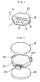
- Fig. 1 is a partly cut-away perspective view illustrating the construction of a magnetic rotor in a three-terminal circulator that is one example of the above circulator.
- Fig. 2 is an exploded perspective view illustrating the general construction of the circulator.
- Fig. 3 is an equivalent circuit diagram for the circulator.
- Figs. 4A, 4B and 4C are views illustrating a part of the fabrication process of the magnetic rotor in the circulator.
- this circulator is of the three-terminal type wherein a magnetic rotor 20 is of a regular hexagonal plane shape. If the magnetic rotor 20 has a structure capable of generating a uniform rotating magnetic field, however, its plane shape is not always limited to the regular hexagonal shape. In other words, the magnetic rotor may be of other hexagonal shape or a polygonal shape. By allowing the magnetic rotor to be of a polygonal plane shape, it is possible to reduce the overall size of the magnetic rotor. This is because when a circuit element such as a resonant capacitor is externally mounted on the side of the magnetic rotor, it is possible to make effective use of an available space.
- a circuit element such as a resonant capacitor
- reference numeral 10 stands for an integrally fired magnetic layer.
- An internal conductor (center conductor) 11 is formed according to a given pattern while it is surrounded with the magnetic layer 10.
- the internal conductor 11 comprises two layers laminated one upon another.
- a set of two layers are each provided with a strip form of coil pattern extending in three radial directions (radial directions perpendicular to at least one side of the hexagon).
- the strip form of coil patterns extending in the same direction on both layers, are electrically connected to each other by way of a via hole conductor. That is, the magnetic layer is also used as an insulator.
- One end of each coil pattern is electrically 5 connected to a terminal electrode 12 formed on every other side of the magnetic layer 10.
- ground conductors ground electrodes 13
- the other end of each coil pattern is electrically connected to the ground conductor 13 on each of the terminal electrode-free sides of the magnetic layer.
- resonant capacitors 21a, 21b and 21c are electrically connected to three terminal electrodes (12) on a magnetic rotor 20.
- a high-frequency capacitor e.g., a feedthrough capacitor having a high self-resonance frequency and proposed by the applicant, such as one disclosed in JP-A 5-251262.
- This high-frequency capacitor has a multilayer triplate ⁇ strip line structure wherein a ground conductor and a dielectric material are superposed in this order on at least one unit of multilayer member comprising a dielectric material, an internal conductor and a dielectric material superposed on a ground conductor in the described order.
- the magnetic rotor 20 is provided on its upper and lower surfaces with exciting permanent magnets 22 and 23 (see Fig. 2) to apply a direct current magnetic field 14 (see Fig. 1) on the magnetic rotor 20.
- an upper sheet 40, an intermediate sheet 41 and a lower sheet 42, all made up of the same insulating magnetic material, are provided.
- Each of the upper and lower sheets 40 and 42 has usually a thickness of about 0.5 to 2 mm, and is built up of a plurality of sheeting materials laminated one upon another, each having a thickness of about 100 to 200 ⁇ m (preferably 160 ⁇ m).
- the intermediate sheet 41 has a thickness of about 30 to 200 ⁇ m, and preferably about 160 ⁇ m.
- Via holes 43a, 43b and 43c are formed through the intermediate sheet 41 at given positions.
- a via hole conductor having a diameter somewhat larger than that of the via hole is provided by means of printing or transfer.
- the via hole conductor it is acceptable to use the same electrical conducting material as that of the internal conductor. However, it is preferable to use a material having a melting point higher than that of the electrical conducting material.
- the intermediate sheet 41 On the upper surface of the intermediate sheet 41 three sets of upper internal conductors 44a, 44b and 44c are provided according to coil patterns by the printing or transfer of internal conductor pastes. Each set comprises two strip form of patterns extending in the same radial directions (radial directions perpendicular to at least one side of the hexagon) while they sidestep the via hole portions.
- On the upper surface of the lower sheet 42 three similar sets of lower internal conductors 45a, 45b and 45c are provided in the same manner as mentioned just above. After the thus formed upper, intermediate and lower sheets 40, 41 and 42 are superposed one upon another, they are stacked together by heating and pressing.
- the coil patterns of thrice symmetry are located on both surfaces of the intermediate sheet 41. It is this symmetry that ensures that the propagation characteristics between the terminals of the three-terminal circulator coincide well with one another.
- the upper, intermediate and lower sheets 40, 41 and 42 stacked as shown in Fig. 4B are fired together at least once at the temperature that is equal to or higher than the melting point of the electrical conducting material and lower than the boiling point of the electrical conducting material.
- firing is carried out two or more times, it is required that at least one firing operation be carried out at the temperature equal to or higher than the above melting point.
- the magnetic materials forming the upper, intermediate and lower sheets 40, 41 and 42 are constructed as an integral continuous member.
- one ends of the upper internal conductors 44a, 44b and 44c are electrically connected to one ends of the lower internal conductors 45a, 45b and 45c by way of the via hole conductors in the via holes 43a, 43b and 4c.
- each magnetic rotor After firing and cutting, each magnetic rotor is subjected to barrel polishing to expose the internal conductors on its sides, and the corners of the sintered body are chamfered. Thereafter, terminal electrodes 46 are baked onto every other sides of the magnetic rotor and ground conductors 47 are baked onto the upper and lower surfaces of the magnetic rotor as well as onto terminal electrode 46-free sides of the magnetic rotor, as shown Fig. 4C.
- the present invention may also be applicable to a circulator having four or more terminals. Further, the present invention may be applicable to not only a lumped constant circulator such as one mentioned above but also to a distributed constant circulator wherein a magnetic rotor is integrated with a capacity circuit and an impedance transducer for making the operating frequency range wide is incorporated in a terminal circuit. Furthermore, a non-reversible circuit element such as an isolator, too, may be easily fabricated by an extension of such a circulator.
- Yttrium oxide (Y 2 O 3 ) and iron oxide (Fe 2 O 3 ) were mixed together at a molar ratio of 3:5.
- the powder mixture was calcined at 1,200°C.
- the obtained calcined powders were pulverized in a ball mill.
- An organic binder and a solvent were added to the powder particles with the addition of silver powders thereto in an amount of 0.2 to 5% by weight, as shown in Table 1, thereby preparing a magnetic slurry.
- the obtained slurry was formed into a green sheet by a doctor blade process.
- the green sheet was punched out by a punching machine to provide therein holes to act as via holes, followed by printing a silver conductor pattern on the green sheet by a thick-film printing process.
- the width of the silver conductor was half of that referred to in WO98/05045.
- the via holes were also filled with silver.
- a paste obtained by the dispersion of silver alone, and a paste comprising silver and 3 mol% of Ga 2 O 3 added thereto were used. Green sheets were thermally pressed to obtain a laminate. Thereafter, the laminate was fired at 1,430°C and then cut into a given size and shape.
- Comparative Example 1 a sample was prepared as in the above examples except for no addition of silver to the magnetic material.
- the capacity substrate 102, ferrite magnet 103 and yoke 104 used were the same as in the prior art.
- the yield of the non-reversible circuit element samples is shown in Table 1. It is here to be noted that 108 samples were prepared. The interior of each sample was observed by a transmission X-ray measuring device. An element showing breaks in the wire and failures over 2/3 of the wire width was judged as a defective. It is to be noted that the average grain size was 3.2 to 5.4 ⁇ m.
- Example 1-1 0.2 ⁇ 99.1
- Example 1-2 0.5 ⁇ 97.2
- Example 1-3 1.0 ⁇ 95.3
- Example 1-4 3.0 ⁇ 94.4
- Example 1-5 5.0 ⁇ 92.6
- Example 1-6 0.2 ⁇ 83.3
- Example 1-7 0.5 ⁇ 81.5
- Example 1-8 1.0 ⁇ 76.9
- Example 1-9 3.0 ⁇ 75.9
- Example 1-10 5.0 ⁇ 72.2 Comp. Ex. 1 0.0 ⁇ 27.8
- Non-reversible circuit elements (Examples 2-1 to 2-10) were obtained as in Example 1 with the exception that for the oxide magnetic material, yttrium oxide (Y 2 O 3 ), iron oxide (Fe 2 O 3 ) and aluminum oxide (Al 2 O 3 ) were mixed together at a molar ratio of 6:9:1.
- the amount of silver added to the magnetic material, and the yield of the non-reversible elements are shown in Table 2.
- the high-frequency characteristics were measured by a network analyzer.
- Example 2 Amount of silver added, % by weight Addition of Ga 2 O 3 to silver conductor Yield, % Example 2-1 0.2 ⁇ 99.1 Example 2-2 0.5 ⁇ 95.4 Example 2-3 1.0 ⁇ 99.1 Example 2-4 3.0 ⁇ 94.4 Example 2-5 5.0 ⁇ 93.5 Example 2-6 0.2 ⁇ 82.4 Example 2-7 0.5 ⁇ 76.9 Example 2-8 1.0 ⁇ 77.8 Example 2-9 3.0 ⁇ 71.3
- Example 2-10 5.0 ⁇ 75.0 Comp. Ex. 2 0.0 ⁇ 23.1
- Non-reversible circuit elements were obtained as in Example 1 with the exception that for the oxide magnetic material, yttrium oxide (Y 2 O 3 ), iron oxide (Fe 2 O 3 ), vanadium oxide (V 2 O 5 ) and calcium oxide (CaCO 3 ) were mixed together at a molar ratio of 11:23:2:8.
- Y 2 O 3 yttrium oxide
- Fe 2 O 3 iron oxide
- V 2 O 5 vanadium oxide
- CaCO 3 calcium oxide
- Example 3 The amount of silver added to the magnetic material, and the yield of the non-reversible elements are shown in Table 3.
- the high-frequency characteristics were measured by a network analyzer.
- Table 3 Amount of silver added, % by weight Addition of Ga 2 O 3 to silver conductor Yield, %
- Example 3-1 0.2 ⁇ 91.7
- Example 3-2 0.5 ⁇ 88.9
- Example 3-3 1.0 ⁇ 86.1
- Example 3-4 3.0 ⁇ 81.5
- Example 3-5 5.0 ⁇ 82.4
- Example 3-6 0.2 ⁇ 71.3
- Example 3-7 0.5 ⁇ 74.1
- Example 3-8 1.0 ⁇ 67.6
- Example 3-9 3.0 ⁇ 69.4
- Example 3-10 5.0 ⁇ 65.7 Comp. Ex. 3 0.0 ⁇ 22.2
- Yields were measured as in Examples 1-1 to 1-5, 2-1 to 2-5 and 3-1 to 3-5 with the exception that La 2 O 3 , Pr 6 O 11 , Sm 2 O 3 , Eu 2 O 3 , Gd 2 O 3 , Dy 2 O 3 , Er 2 O 3 , Tm 2 O 3 , and Yb 2 O 3 were used instead of Ga 2 O 3 . Equivalent effects were obtained.
Landscapes
- Soft Magnetic Materials (AREA)
- Non-Reversible Transmitting Devices (AREA)
- Ceramic Capacitors (AREA)
- Coils Or Transformers For Communication (AREA)
Description
- The present invention relates to a multilayer ceramic part.
- With recent breakthroughs in radio communications technologies, there is an increasing demand for electronic parts that can be used at high frequencies ranging from a few hundred MHz to a few GHz or greater. With size reductions of radio communications equipment such as portable telephones, there is also a strong demand for size, and cost reductions of high frequency-conscious electronic parts used with such equipment. To meet these requirements, multilayer ceramic parts are now manufactured by the application of a diversity of integration technologies.
- A multilayer electronic part is obtained by co-firing a ceramic material that is an oxide magnetic material and a conductive material, and has one or two or more functions by itself. Such a multilayer electronic part is manufactured by laminating the ceramic and conductive materials one upon another by printing or sheet-making processes to form a laminate, and cutting the laminate according to the desired shape and size followed by firing, or firing the laminate followed by cutting according to the desired shape and size. If required, an external conductor is provided on the electronic part. Thus, this multilayer ceramic part has a structure comprising an internal conductor between ceramic layers. In general, a material such as Ag or Cu is used for an internal conductor suitable for high-frequencies, especially microwaves. With the above production method, however, it has been considered until now that the melting of the internal conductor should be prevented so as to achieve satisfactory properties, and so firing should be carried out at a temperature equal to or lower than the melting point of the internal conductor. Accordingly, it has been believed that a ceramic material fired at elevated temperatures cannot possibly be used in combination with an internal conductor-forming electrical conducting material having a low resistivity yet a low melting point, e.g., Ag, and Cu.
- In this regard, the applicant has filed a Japanese patent application (JP-A 6-252618) to come up with a method wherein an internal conductor having a low melting point as mentioned above is formed in a ceramic material unsuitable for low-temperature firing. This is called a conductor melting method wherein an electrical conducting material to form an internal conductor is fired at a temperature that is equal to or higher than the melting point of the electrical conducting material and lower than the boiling point of the electrical conducting material, and solidifying the fired electrical conducting material in the process of cooling. According to this method, the grain boundary between metal grains formed upon the solidification of the molten electrical conducting material becomes as thin as can be regarded as vanishing substantially, and the asperity of the interface between the ceramic material and the internal conductor tends to become small, resulting in a decrease in the high-frequency resistance of the internal conductor and an increase in the Q value at a high-frequency region. Further, a low-cost electrical conducting material having a relatively low melting point, e.g., Ag, and Cu may be used for the internal conductor. Furthermore, it is possible to co-fire the ceramic material and the internal conductor. These are very favorable in view of productivity and cost.
- With the above conductor melting method, however, voids are often formed in the internal conductor upon the solidification of the internal conductor material in the cooling process subsequent to the melting of the internal conductor material. This in turn causes the resistance value of the internal conductor to increase with a decrease in the Q value of the multilayer ceramic part. On very rare occasions, the internal conductor itself breaks due to the presence of such voids. When there are voids in the internal conductor, gases present in the voids expand under the influence of latent heat of solidification in the cooling process, resulting in cracking of the internal conductor material. This in turn gives rise to an yield drop. When a multilayer ceramic part is manufactured by the conductor melting method, therefore, it is required to inhibit the formation of voids in the internal conductor.
- For the purpose of providing a high-quality conductive paste which can prevent formation of voids, and generation of cracking due to such voids, even when an internal conductor composed mainly of silver is co-fired with a ceramic material by the conductor melting method, and so improve productivity with cost reductions, and which has excellent electrical characteristics as well as a multilayer ceramic part obtained using such a conductive paste, the applicant has proposed in WO98/05045 such a conductive paste as mentioned below as well as a multilayer ceramic part comprising an internal conductor formed using this conductive paste.
- That is, the above conductive paste is a conductive paste obtained by dispersing an electrical conducting material composed mainly of silver and a metal oxide in a vehicle. For the metal oxide, at least one oxide selected from Ga, La, Pr, Sm, Eu, Gd, Dy, Er, Tm and Yb oxides is used.
- When a multilayer ceramic part is fabricated by using this conductive paste, i.e., by co-firing the conductive paste and a ceramic material by the conductor melting method, no voids are generated; the ceramic material is quite unlikely to crack. The resistivity of the conductor, too, is low. By use of this conductive paste, it is thus possible to fabricate a multilayer ceramic part of very excellent quality in high yields.
- However, multilayer ceramic parts having such applications as mentioned above, too, are now increasingly required to be further reduced in size in conjunction with the demand for size reductions of mobile communications equipment in particular.
- This invention seeks to provide a multilayer ceramic part which, albeit being reduced in size, can be manufactured in high yields.
- The scope of this invention is defined by the attached set of claims.
- In the multilayer ceramic part of the invention comprising an internal conductor layer and a ceramic layer which are formed by co-firing, the internal conductor layer is formed of an electrical conducting material containing silver as a main component and the ceramic layer is formed of an yttrium-iron-garnet based oxide magnetic material with silver added thereto. Under the action of this silver, the formation of voids, etc. in the internal conductor layer is reduced as much as possible, resulting in an part yield improvement.
-
- Figure 1 is a partly cut-away perspective view illustrating schematically the construction of a magnetic rotor in a three-terminal circulator.
- Figure 2 is an exploded perspective view illustrating the general construction of a three-terminal circulator.
- Figure 3 is an equivalent circuit diagram for the three-terminal circulator shown in Fig. 2.
- Figures 4A, 4B and 4C are views illustrating a part of the fabrication process of the magnetic rotor shown in Fig. 1.
- Figures 5A, 5B and 5C are views for illustrating the structure of one non-reversible circuit element fabricated in the examples.
- The present invention is now explained in further detail.
- The multilayer ceramic part of the invention comprises an internal conductor layer and ceramic layers.
- When the multilayer ceramic part is fabricated, a conductive paste sandwiched between ceramic material layers is fired at a temperature that is equal to or higher than the melting point of the electrical conducting material and lower than the boiling point of the electrical conducting material, thereby forming the internal conductor layer and the ceramic layers. The conductive paste is obtained by dispersing the electrical conducting material containing silver as a main component in a vehicle. Preferably in this case, a given metal oxide is further dispersed in the vehicle.
- The electrical conducting material containing silver as the main component may be silver alone or a mixture of silver with other metal capable of forming a solid solution therewith, for instance, copper, gold, palladium, and platinum. When these additive metals are used, the content of silver in the electrical conducting material should be at least 70 mol%. The reason is that the amount of the mixture exceeds 30 mol%, the resistivity of the alloy is greater than that of silver. More preferably or to reduce fabrication cost increases, the amount of the additive metal mixed with silver should be up to 5 mol% (or the content of silver should be at least 95 mol%).
- At least one metal oxide selected from the Ga oxide (Ga2O3), La oxide (La2O3), Pr oxide (Pr6O11), Sm oxide (Sm2O3), Eu oxide (Eu2O3), Gd oxide (Gd2O3), Dy oxide (Dy2O3), Er oxide (Er2O3), Tm oxide (Tm2O3), and Yb oxide (Yb2O3) may be used as the metal oxide. The reason is that these metal oxides react with, and diffuse into, the ceramic material. When, in this case, the content of the metal oxide(s) per 100 parts by weight of the electrical conducting material is below 0.1 part by weight, no sufficient reaction phase is formed at the interface, resulting in a silver wettability drop. At greater than 20 parts by weight, the metal oxide(s) remains in the internal conductor due to its imperfect diffusion, resulting in a conductor resistance increase. For this reason, it is preferred that the content of the metal oxide(s) is in the range of 0.1 to 20 parts by weight per 100 parts by weight of the electrical conducting material. While the electrical conducting material is not critical in terms of particle size, it should preferably have an average particle size of 0.1 to 20 µm when the conductor is formed by a screen printing process. For similar reasons, the metal oxide(s) should preferably have an average particle size of 0.1 to 20 µm.
- For the vehicle, a binder such as ethyl cellulose, nitrocellulose and acrylic resin, and an organic solvent such as terpineol, butyl carbitol and hexyl carbitol may be used optionally with dispersants, activators, etc. added thereto. It is here to be noted that the vehicle content of the conductive paste should preferably be in the range of 5 to 70% by weight. It is also preferable that the conductive paste is regulated to a viscosity of about 300 to 30,000 cps (centipoise).
- For the magnetic material used to form the ceramic layer, a garnet type ferrite for high-frequency purposes is generally used. The garnet type ferrite for high-frequency purposes is preferably a substituted type garnet ferrite having a fundamental composition based on YIG (yttrium-iron-garnet), specifically Y3Fe5O12, to which various elements are added. If the composition of the substituted type garnet ferrite is represented by
(Y3-xαx) (Fe5-yβy)O12
it is then preferable that the element α, by which Y is substituted, is at least one element of Ca, Bi, and Gd. For the purpose of property improvements in this case, it is preferable to use at least one element of Ho, Dy, and Ce as a trace additive. The element β, by which Fe is substituted, is preferably at least one element of V, Al, Ge, Ga, Sn, Zr, Ti, and In. For the purpose of property improvements in this case, it is preferable to use at least one element of Mn, Co, and Si as a trace additive. The amount of substitution is then preferably


It is here to be noted that the atomic ratio of the trace additive used for property improvements in the above formula is usually 0.2 or less, and that the ratio, (substituent element-containing Y):(substituent element-containing Fe):O may deviate from the stoichiometric composition ratio of 3:5:12. It is also to be noted that the garnet ferrite has an average grain size of about 1 to 10 µm. - A magnetic material sheet may be formed using a magnetic paste containing a magnetic material and a vehicle.
- For the vehicle, mention is made of a binder such as ethyl cellulose, polyvinyl butyral, methacrylic resin and butyl methacrylate and a solvent such as terpineol, butyl carbitol, butyl carbitol acetate, acetate, toluene, alcohol and xylene as well as various dispersants, activators, plasticizers, etc., from which any desired vehicle may be selected depending on the purpose. The amount of the vehicle added is about 65 to 85% by weight per a total of 100 parts by weight of the oxide aggregate and glass.
- According to the invention, silver is added into the above magnetic paste. The content of silver in the magnetic material is up to 10% by weight, preferably up to 5% by weight, more preferably 3% by weight, and even more preferably 1% by weight. The silver, even when used in a very small amount, is found to be effective. The lower limit to the amount of silver added is not particularly specified, although the amount of silver added should not be zero. However, it is preferable that the lower limit is 0.1% by weight, and especially 0.2% by weight.
- The silver in a particulate form should preferably be added into the magnetic paste. Preferably in this case, the silver should have an average particle size of 2.5 to 4.5 µm. It is here to be noted that the silver is usually present at the grain boundary after firing.
- According to the invention, various multilayer ceramic parts are obtained by laminating the conductive paste and ceramic material one upon another by known processes such as a printing process or a sheet-making process to form a green laminate, and firing the laminate at a temperature that is equal to or higher than the melting point of the electrical conducting material and lower than the boiling point of the electrical conducting material. For instance, chip capacitors, chip inductors, non-reversible circuit elements (circulators, and isolators), LC filters, semiconductor capacitors, and glass ceramic multilayer boards may be fabricated.
- The present invention is now explained specifically with reference to a circulator of the non-reversible circuit elements, to which the invention is preferably applied. A preferable circulator to which the invention is applied, for instance, is disclosed in US 08/219,917 (USP 5,450,045). This circulator comprises a magnetic rotor. The magnetic rotor comprises an internal conductor, an insulating magnetic body fired integrally with the internal conductor while it is in close contact with the internal conductor and surrounds the internal conductor, a plurality of terminal electrodes electrically connected to one end of the internal conductor, a plurality of capacitors coupled to the terminal electrodes for resonance with an applied frequency, and an exciting permanent magnet for applying a direct current magnetic field on the magnetic rotor. In the circulator of this construction, no demagnetizing field is generated because a high-frequency magnetic flux forms a closed loop in the magnetic rotor due to the absence of discontinuities in the magnetic body. Accordingly, the circulator can be reduced in size and cost, and can be used at a wider band yet with reduced losses.
- Fig. 1 is a partly cut-away perspective view illustrating the construction of a magnetic rotor in a three-terminal circulator that is one example of the above circulator. Fig. 2 is an exploded perspective view illustrating the general construction of the circulator. Fig. 3 is an equivalent circuit diagram for the circulator. Figs. 4A, 4B and 4C are views illustrating a part of the fabrication process of the magnetic rotor in the circulator.
- As illustrated, this circulator is of the three-terminal type wherein a
magnetic rotor 20 is of a regular hexagonal plane shape. If themagnetic rotor 20 has a structure capable of generating a uniform rotating magnetic field, however, its plane shape is not always limited to the regular hexagonal shape. In other words, the magnetic rotor may be of other hexagonal shape or a polygonal shape. By allowing the magnetic rotor to be of a polygonal plane shape, it is possible to reduce the overall size of the magnetic rotor. This is because when a circuit element such as a resonant capacitor is externally mounted on the side of the magnetic rotor, it is possible to make effective use of an available space. - In Fig. 1,
reference numeral 10 stands for an integrally fired magnetic layer. An internal conductor (center conductor) 11 is formed according to a given pattern while it is surrounded with themagnetic layer 10. In this embodiment, theinternal conductor 11 comprises two layers laminated one upon another. A set of two layers are each provided with a strip form of coil pattern extending in three radial directions (radial directions perpendicular to at least one side of the hexagon). The strip form of coil patterns, extending in the same direction on both layers, are electrically connected to each other by way of a via hole conductor. That is, the magnetic layer is also used as an insulator. One end of each coil pattern is electrically 5 connected to aterminal electrode 12 formed on every other side of themagnetic layer 10. The upper and lower surfaces of themagnetic layer 10, and terminal electrode-free sides of themagnetic layer 10 are provided with ground conductors (ground electrodes) 13. The other end of each coil pattern is electrically connected to theground conductor 13 on each of the terminal electrode-free sides of the magnetic layer. - As can be seen from Fig. 2 illustrating the general construction of the circulator,
resonant capacitors magnetic rotor 20. For these capacitors, it is preferable to use a high-frequency capacitor, e.g., a feedthrough capacitor having a high self-resonance frequency and proposed by the applicant, such as one disclosed in JP-A 5-251262. This high-frequency capacitor has a multilayer triplate·strip line structure wherein a ground conductor and a dielectric material are superposed in this order on at least one unit of multilayer member comprising a dielectric material, an internal conductor and a dielectric material superposed on a ground conductor in the described order. By use of such a feedthrough capacitor having a wide range of operating frequency, it is possible to prevent a Q value drop. It is here to be noted that the connections between the terminal electrodes and the capacitors are the same as shown in the equivalent circuit diagram attached hereto as Fig. 3. - The
magnetic rotor 20 is provided on its upper and lower surfaces with excitingpermanent magnets 22 and 23 (see Fig. 2) to apply a direct current magnetic field 14 (see Fig. 1) on themagnetic rotor 20. - The fabrication process of the circulator having such construction is now explained.
- As shown in Fig. 4A, an
upper sheet 40, anintermediate sheet 41 and alower sheet 42, all made up of the same insulating magnetic material, are provided. Each of the upper andlower sheets intermediate sheet 41 has a thickness of about 30 to 200 µm, and preferably about 160 µm. - Via
holes intermediate sheet 41 at given positions. At each via hole position a via hole conductor having a diameter somewhat larger than that of the via hole is provided by means of printing or transfer. For the via hole conductor, it is acceptable to use the same electrical conducting material as that of the internal conductor. However, it is preferable to use a material having a melting point higher than that of the electrical conducting material. - On the upper surface of the
intermediate sheet 41 three sets of upperinternal conductors lower sheet 42 three similar sets of lowerinternal conductors lower sheets intermediate sheet 41. It is this symmetry that ensures that the propagation characteristics between the terminals of the three-terminal circulator coincide well with one another. - The upper, intermediate and
lower sheets lower sheets - While the upper, intermediate and
lower sheets - By the firing operation(s) as mentioned above, one ends of the upper
internal conductors internal conductors holes - After firing and cutting, each magnetic rotor is subjected to barrel polishing to expose the internal conductors on its sides, and the corners of the sintered body are chamfered. Thereafter,
terminal electrodes 46 are baked onto every other sides of the magnetic rotor andground conductors 47 are baked onto the upper and lower surfaces of the magnetic rotor as well as onto terminal electrode 46-free sides of the magnetic rotor, as shown Fig. 4C. This ensures that the other ends of the upperinternal conductors internal conductors resonant capacitors - While the above embodiment has been explained with reference to a three-terminal type circulator, it is to be understood that the present invention may also be applicable to a circulator having four or more terminals. Further, the present invention may be applicable to not only a lumped constant circulator such as one mentioned above but also to a distributed constant circulator wherein a magnetic rotor is integrated with a capacity circuit and an impedance transducer for making the operating frequency range wide is incorporated in a terminal circuit. Furthermore, a non-reversible circuit element such as an isolator, too, may be easily fabricated by an extension of such a circulator.
- The present invention is now explained with reference to specific examples.
- Yttrium oxide (Y2O3) and iron oxide (Fe2O3) were mixed together at a molar ratio of 3:5. The powder mixture was calcined at 1,200°C. The obtained calcined powders were pulverized in a ball mill. An organic binder and a solvent were added to the powder particles with the addition of silver powders thereto in an amount of 0.2 to 5% by weight, as shown in Table 1, thereby preparing a magnetic slurry. The obtained slurry was formed into a green sheet by a doctor blade process. The green sheet was punched out by a punching machine to provide therein holes to act as via holes, followed by printing a silver conductor pattern on the green sheet by a thick-film printing process. Here and hereafter, the width of the silver conductor was half of that referred to in WO98/05045. At the same time, the via holes were also filled with silver. For the printing paste, a paste obtained by the dispersion of silver alone, and a paste comprising silver and 3 mol% of Ga2O3 added thereto were used. Green sheets were thermally pressed to obtain a laminate. Thereafter, the laminate was fired at 1,430°C and then cut into a given size and shape.
- Then, silver pastes were baked onto the upper and lower surfaces of the fired laminate to form ground electrodes thereon. Further, silver pastes were baked onto the sides of the fired laminate to form electrodes for making connections between terminal electrodes and the upper and lower ground electrodes. In this way, there was obtained a magnetic rotor in which the magnetic bodies were integrated with the center conductors. A
magnetic rotor 101, acapacity substrate 102, aferrite magnet 103 and ayoke 104 were assembled together in accordance with the layouts illustrated in Figs. 5A, 5B, and 5C. In this way, non-reversible circuit element samples were obtained (Examples 1-1 to 1-10). In Comparative Example 1, a sample was prepared as in the above examples except for no addition of silver to the magnetic material. In the above examples and comparative example as well as in the following examples and comparative examples, thecapacity substrate 102,ferrite magnet 103 andyoke 104 used were the same as in the prior art. The yield of the non-reversible circuit element samples is shown in Table 1. It is here to be noted that 108 samples were prepared. The interior of each sample was observed by a transmission X-ray measuring device. An element showing breaks in the wire and failures over 2/3 of the wire width was judged as a defective. It is to be noted that the average grain size was 3.2 to 5.4 µm.Table 1 Amount of silver added, % by weight Addition of Ga2O3 to silver conductor Yield, % Example 1-1 0.2 ○ 99.1 Example 1-2 0.5 ○ 97.2 Example 1-3 1.0 ○ 95.3 Example 1-4 3.0 ○ 94.4 Example 1-5 5.0 ○ 92.6 Example 1-6 0.2 × 83.3 Example 1-7 0.5 × 81.5 Example 1-8 1.0 × 76.9 Example 1-9 3.0 × 75.9 Example 1-10 5.0 × 72.2 Comp. Ex. 1 0.0 ○ 27.8 - Non-reversible circuit elements (Examples 2-1 to 2-10) were obtained as in Example 1 with the exception that for the oxide magnetic material, yttrium oxide (Y2O3), iron oxide (Fe2O3) and aluminum oxide (Al2O3) were mixed together at a molar ratio of 6:9:1. The amount of silver added to the magnetic material, and the yield of the non-reversible elements are shown in Table 2. The high-frequency characteristics were measured by a network analyzer.
Table 2 Amount of silver added, % by weight Addition of Ga2O3 to silver conductor Yield, % Example 2-1 0.2 ○ 99.1 Example 2-2 0.5 ○ 95.4 Example 2-3 1.0 ○ 99.1 Example 2-4 3.0 ○ 94.4 Example 2-5 5.0 ○ 93.5 Example 2-6 0.2 × 82.4 Example 2-7 0.5 × 76.9 Example 2-8 1.0 × 77.8 Example 2-9 3.0 × 71.3 Example 2-10 5.0 × 75.0 Comp. Ex. 2 0.0 ○ 23.1 - Non-reversible circuit elements were obtained as in Example 1 with the exception that for the oxide magnetic material, yttrium oxide (Y2O3), iron oxide (Fe2O3), vanadium oxide (V2O5) and calcium oxide (CaCO3) were mixed together at a molar ratio of 11:23:2:8.
- The amount of silver added to the magnetic material, and the yield of the non-reversible elements are shown in Table 3. The high-frequency characteristics were measured by a network analyzer.
Table 3 Amount of silver added, % by weight Addition of Ga2O3 to silver conductor Yield, % Example 3-1 0.2 ○ 91.7 Example 3-2 0.5 ○ 88.9 Example 3-3 1.0 ○ 86.1 Example 3-4 3.0 ○ 81.5 Example 3-5 5.0 ○ 82.4 Example 3-6 0.2 × 71.3 Example 3-7 0.5 × 74.1 Example 3-8 1.0 × 67.6 Example 3-9 3.0 × 69.4 Example 3-10 5.0 × 65.7 Comp. Ex. 3 0.0 ○ 22.2 - Yields were measured as in Examples 1-1 to 1-5, 2-1 to 2-5 and 3-1 to 3-5 with the exception that La2O3, Pr6O11, Sm2O3, Eu2O3, Gd2O3, Dy2O3, Er2O3, Tm2O3, and Yb2O3 were used instead of Ga2O3. Equivalent effects were obtained.
- From the foregoing, the effectiveness of the present invention is obvious.
Claims (7)
- A multilayer ceramic part comprising an internal conductor layer and a ceramic layer which are formed by co-firing, wherein said internal conductor layer is formed of an electrical conducting material containing silver as a main component and said ceramic layer is formed of an yttrium-iron-garnet based oxide magnetic material with silver added thereto in an amount of at least 0.1% by weight and up to 10% by weight.
- A multilayer ceramic part as claimed in claim 1, wherein said silver is added to said oxide magnetic material in an amount of up to 5% by weight.
- A multilayer ceramic part as claimed in either claim 1 or claim 2, wherein said silver is added to said oxide magnetic material in an amount at least 0.2% by weight.
- A multilayer ceramic part as claimed in any one of the preceding claims, wherein said internal conductor layer is formed by firing a conductive paste obtained by dispersing in a vehicle an electrical conducting material containing silver as a main component and further containing at least one metal oxide selected from a Ga oxide, an La oxide, a Pr oxide, an Sm oxide, an Eu oxide, a Gd oxide, a Dy oxide, an Er oxide, a Tm oxide, and a Yb oxide.
- A multilayer ceramic part as claimed in claim 4, wherein said metal oxide is in the range 0.1 to 20 parts by weight per 100 parts by weight of said electrical conducting material.
- A multilayer ceramic part as claimed in any one of the preceding claims, wherein the part is formed by firing at a temperature equal to or higher than the melting point of said electrical conducting material and lower than the boiling point of said electrical conducting material.
- A multilayer ceramic part as claimed in any one of the preceding claims, which is a non-reversible circuit element.
Applications Claiming Priority (5)
| Application Number | Priority Date | Filing Date | Title |
|---|---|---|---|
| JP27517597 | 1997-09-22 | ||
| JP27517597 | 1997-09-22 | ||
| JP32690997 | 1997-11-12 | ||
| JP9326909A JPH11154805A (en) | 1997-09-22 | 1997-11-12 | Laminated ceramic part |
| PCT/JP1998/004208 WO1999016089A1 (en) | 1997-09-22 | 1998-09-18 | Laminated ceramic parts |
Publications (3)
| Publication Number | Publication Date |
|---|---|
| EP0940825A1 EP0940825A1 (en) | 1999-09-08 |
| EP0940825A4 EP0940825A4 (en) | 2001-05-23 |
| EP0940825B1 true EP0940825B1 (en) | 2006-04-05 |
Family
ID=26551354
Family Applications (1)
| Application Number | Title | Priority Date | Filing Date |
|---|---|---|---|
| EP98943039A Expired - Lifetime EP0940825B1 (en) | 1997-09-22 | 1998-09-18 | Laminated ceramic parts |
Country Status (6)
| Country | Link |
|---|---|
| US (1) | US6235221B1 (en) |
| EP (1) | EP0940825B1 (en) |
| JP (1) | JPH11154805A (en) |
| CN (1) | CN1111881C (en) |
| DE (1) | DE69834098T2 (en) |
| WO (1) | WO1999016089A1 (en) |
Families Citing this family (8)
| Publication number | Priority date | Publication date | Assignee | Title |
|---|---|---|---|---|
| JP3744739B2 (en) * | 1999-07-30 | 2006-02-15 | 京セラ株式会社 | Multilayer ceramic capacitor |
| GB2370569B (en) * | 1999-12-13 | 2003-03-05 | Murata Manufacturing Co | Monolithic ceramic electronic component and production process therefor |
| JP3767362B2 (en) | 1999-12-13 | 2006-04-19 | 株式会社村田製作所 | Manufacturing method of multilayer ceramic electronic component |
| JP2001345212A (en) * | 2000-05-31 | 2001-12-14 | Tdk Corp | Laminated electronic part |
| JP3939622B2 (en) * | 2002-09-20 | 2007-07-04 | アルプス電気株式会社 | Non-reciprocal circuit element, isolator, and non-reciprocal circuit element manufacturing method |
| JP2007234893A (en) * | 2006-03-01 | 2007-09-13 | Tdk Corp | Coil part |
| CN107034517A (en) * | 2011-06-06 | 2017-08-11 | 天工方案公司 | Modified garnet structure and radio system |
| JP6812722B2 (en) * | 2016-09-30 | 2021-01-13 | 住友金属鉱山株式会社 | Evaluation method of internal electrode film of laminated ceramic electronic component and manufacturing method of laminated ceramic electronic component |
Family Cites Families (9)
| Publication number | Priority date | Publication date | Assignee | Title |
|---|---|---|---|---|
| JPH04354315A (en) * | 1991-05-31 | 1992-12-08 | Kokusai Electric Co Ltd | Thick-film capacitor |
| JPH04354314A (en) * | 1991-05-31 | 1992-12-08 | Taiyo Yuden Co Ltd | Manufacture of laminated ceramic inductor |
| US5312674A (en) * | 1992-07-31 | 1994-05-17 | Hughes Aircraft Company | Low-temperature-cofired-ceramic (LTCC) tape structures including cofired ferromagnetic elements, drop-in components and multi-layer transformer |
| JP2858073B2 (en) | 1992-12-28 | 1999-02-17 | ティーディーケイ株式会社 | Multilayer ceramic parts |
| US5450045A (en) * | 1993-03-31 | 1995-09-12 | Tdk Corporation | Multi-layer microwave circulator |
| JP3405013B2 (en) * | 1995-10-06 | 2003-05-12 | 松下電器産業株式会社 | Method for producing magnetic material and high-frequency circuit component using the same |
| US5709811A (en) * | 1995-04-11 | 1998-01-20 | Matsushita Electric Industrial Co., Ltd. | Magnetic material for microwave and high-frequency circuit component using the same |
| JPH09181412A (en) | 1995-12-22 | 1997-07-11 | Tdk Corp | Multilayer ceramic component |
| EP0853321B1 (en) * | 1996-07-26 | 2004-04-14 | TDK Corporation | Multilayer ceramic part using a conductor paste |
-
1997
- 1997-11-12 JP JP9326909A patent/JPH11154805A/en active Pending
-
1998
- 1998-09-18 WO PCT/JP1998/004208 patent/WO1999016089A1/en active IP Right Grant
- 1998-09-18 CN CN98801384A patent/CN1111881C/en not_active Expired - Fee Related
- 1998-09-18 EP EP98943039A patent/EP0940825B1/en not_active Expired - Lifetime
- 1998-09-18 DE DE69834098T patent/DE69834098T2/en not_active Expired - Fee Related
-
1999
- 1999-05-20 US US09/315,156 patent/US6235221B1/en not_active Expired - Fee Related
Also Published As
| Publication number | Publication date |
|---|---|
| DE69834098D1 (en) | 2006-05-18 |
| WO1999016089A1 (en) | 1999-04-01 |
| JPH11154805A (en) | 1999-06-08 |
| EP0940825A1 (en) | 1999-09-08 |
| CN1239579A (en) | 1999-12-22 |
| US6235221B1 (en) | 2001-05-22 |
| DE69834098T2 (en) | 2006-11-23 |
| CN1111881C (en) | 2003-06-18 |
| EP0940825A4 (en) | 2001-05-23 |
Similar Documents
| Publication | Publication Date | Title |
|---|---|---|
| US7479862B2 (en) | Ferrite material and ceramic substrate | |
| CN101304960B (en) | Polycrystalline ceramic magnetic material, microwave magnetic components, and irreversible circuit devices made by using the same | |
| JP2011073937A (en) | Polycrystal magnetic ceramic, microwave magnetic substance, and irreversible circuit element using the same | |
| JP5126616B2 (en) | Magnetic ceramic, ceramic electronic component, and method of manufacturing ceramic electronic component | |
| EP0940825B1 (en) | Laminated ceramic parts | |
| JP5365967B2 (en) | Polycrystalline ceramic magnetic material, microwave magnetic material, and non-reciprocal circuit device using the same | |
| US6624713B2 (en) | Magnetic material for high frequencies and high-frequency circuit component | |
| EP0853321B1 (en) | Multilayer ceramic part using a conductor paste | |
| JPH11283821A (en) | Nonreversible circuit element | |
| US7522013B2 (en) | Non-reciprocal circuit device | |
| JP2010083689A (en) | Polycrystalline ceramic magnetic material, microwave magnetic substance, and non-reversible circuit component using the same | |
| EP0967621B1 (en) | Conductor paste and nonreversible circuit elements made by using the same | |
| JPH10308118A (en) | Conductive paste, ceramic structure using the same and manufacture of the structure | |
| JP3407725B2 (en) | Oxide magnetic material, method of manufacturing the same, and multilayer chip inductor | |
| JP3523363B2 (en) | Manufacturing method of magnetic sintered body of polycrystalline ceramics and high frequency circuit component using magnetic body obtained by the method | |
| Liu et al. | Low‐Temperature Co‐Fired Magnetoceramics for RF Applications | |
| JP3405013B2 (en) | Method for producing magnetic material and high-frequency circuit component using the same | |
| JP4355629B2 (en) | Superconducting device and manufacturing method thereof | |
| US6645394B2 (en) | High frequency magnetic material ceramic composition and irreversible circuit component | |
| CN113539610A (en) | Laminated coil component | |
| JPH0922615A (en) | Conductor material and laminated ceramic part | |
| JPH11307335A (en) | Magnetic oxide material, multilayer chip inductor and manufacturing method thereof | |
| JPH0945518A (en) | Magnetic material for microwaves and high-frequency circuit component using the same |
Legal Events
| Date | Code | Title | Description |
|---|---|---|---|
| PUAI | Public reference made under article 153(3) epc to a published international application that has entered the european phase |
Free format text: ORIGINAL CODE: 0009012 |
|
| 17P | Request for examination filed |
Effective date: 19990614 |
|
| AK | Designated contracting states |
Kind code of ref document: A1 Designated state(s): DE FR GB NL |
|
| A4 | Supplementary search report drawn up and despatched |
Effective date: 20010411 |
|
| AK | Designated contracting states |
Kind code of ref document: A4 Designated state(s): DE FR GB NL |
|
| RIC1 | Information provided on ipc code assigned before grant |
Free format text: 7H 01F 1/34 A, 7H 01F 17/00 B, 7H 01F 41/16 B, 7H 01P 1/387 B, 7H 01P 11/00 B, 7H 03H 2/00 B |
|
| 17Q | First examination report despatched |
Effective date: 20040729 |
|
| GRAP | Despatch of communication of intention to grant a patent |
Free format text: ORIGINAL CODE: EPIDOSNIGR1 |
|
| GRAS | Grant fee paid |
Free format text: ORIGINAL CODE: EPIDOSNIGR3 |
|
| GRAA | (expected) grant |
Free format text: ORIGINAL CODE: 0009210 |
|
| AK | Designated contracting states |
Kind code of ref document: B1 Designated state(s): DE FR GB NL |
|
| REG | Reference to a national code |
Ref country code: GB Ref legal event code: FG4D |
|
| REF | Corresponds to: |
Ref document number: 69834098 Country of ref document: DE Date of ref document: 20060518 Kind code of ref document: P |
|
| ET | Fr: translation filed | ||
| PLBE | No opposition filed within time limit |
Free format text: ORIGINAL CODE: 0009261 |
|
| STAA | Information on the status of an ep patent application or granted ep patent |
Free format text: STATUS: NO OPPOSITION FILED WITHIN TIME LIMIT |
|
| 26N | No opposition filed |
Effective date: 20070108 |
|
| PGFP | Annual fee paid to national office [announced via postgrant information from national office to epo] |
Ref country code: DE Payment date: 20070913 Year of fee payment: 10 |
|
| PGFP | Annual fee paid to national office [announced via postgrant information from national office to epo] |
Ref country code: GB Payment date: 20070912 Year of fee payment: 10 |
|
| PGFP | Annual fee paid to national office [announced via postgrant information from national office to epo] |
Ref country code: NL Payment date: 20070916 Year of fee payment: 10 |
|
| PGFP | Annual fee paid to national office [announced via postgrant information from national office to epo] |
Ref country code: FR Payment date: 20070914 Year of fee payment: 10 |
|
| GBPC | Gb: european patent ceased through non-payment of renewal fee |
Effective date: 20080918 |
|
| PG25 | Lapsed in a contracting state [announced via postgrant information from national office to epo] |
Ref country code: NL Free format text: LAPSE BECAUSE OF NON-PAYMENT OF DUE FEES Effective date: 20090401 |
|
| NLV4 | Nl: lapsed or anulled due to non-payment of the annual fee |
Effective date: 20090401 |
|
| REG | Reference to a national code |
Ref country code: FR Ref legal event code: ST Effective date: 20090529 |
|
| PG25 | Lapsed in a contracting state [announced via postgrant information from national office to epo] |
Ref country code: DE Free format text: LAPSE BECAUSE OF NON-PAYMENT OF DUE FEES Effective date: 20090401 |
|
| PG25 | Lapsed in a contracting state [announced via postgrant information from national office to epo] |
Ref country code: FR Free format text: LAPSE BECAUSE OF NON-PAYMENT OF DUE FEES Effective date: 20080930 |
|
| PG25 | Lapsed in a contracting state [announced via postgrant information from national office to epo] |
Ref country code: GB Free format text: LAPSE BECAUSE OF NON-PAYMENT OF DUE FEES Effective date: 20080918 |