EP0942259A1 - Capacitive distance sensor - Google Patents
Capacitive distance sensor Download PDFInfo
- Publication number
- EP0942259A1 EP0942259A1 EP99301681A EP99301681A EP0942259A1 EP 0942259 A1 EP0942259 A1 EP 0942259A1 EP 99301681 A EP99301681 A EP 99301681A EP 99301681 A EP99301681 A EP 99301681A EP 0942259 A1 EP0942259 A1 EP 0942259A1
- Authority
- EP
- European Patent Office
- Prior art keywords
- capacitor
- capacitor plate
- sensor
- sensor device
- cell
- Prior art date
- Legal status (The legal status is an assumption and is not a legal conclusion. Google has not performed a legal analysis and makes no representation as to the accuracy of the status listed.)
- Granted
Links
Images


Classifications
-
- G—PHYSICS
- G01—MEASURING; TESTING
- G01B—MEASURING LENGTH, THICKNESS OR SIMILAR LINEAR DIMENSIONS; MEASURING ANGLES; MEASURING AREAS; MEASURING IRREGULARITIES OF SURFACES OR CONTOURS
- G01B7/00—Measuring arrangements characterised by the use of electric or magnetic techniques
- G01B7/02—Measuring arrangements characterised by the use of electric or magnetic techniques for measuring length, width or thickness
- G01B7/023—Measuring arrangements characterised by the use of electric or magnetic techniques for measuring length, width or thickness for measuring distance between sensor and object
-
- G—PHYSICS
- G01—MEASURING; TESTING
- G01B—MEASURING LENGTH, THICKNESS OR SIMILAR LINEAR DIMENSIONS; MEASURING ANGLES; MEASURING AREAS; MEASURING IRREGULARITIES OF SURFACES OR CONTOURS
- G01B7/00—Measuring arrangements characterised by the use of electric or magnetic techniques
- G01B7/004—Measuring arrangements characterised by the use of electric or magnetic techniques for measuring coordinates of points
-
- G—PHYSICS
- G01—MEASURING; TESTING
- G01B—MEASURING LENGTH, THICKNESS OR SIMILAR LINEAR DIMENSIONS; MEASURING ANGLES; MEASURING AREAS; MEASURING IRREGULARITIES OF SURFACES OR CONTOURS
- G01B7/00—Measuring arrangements characterised by the use of electric or magnetic techniques
- G01B7/28—Measuring arrangements characterised by the use of electric or magnetic techniques for measuring contours or curvatures
- G01B7/287—Measuring arrangements characterised by the use of electric or magnetic techniques for measuring contours or curvatures using a plurality of fixed, simultaneously operating transducers
-
- G—PHYSICS
- G01—MEASURING; TESTING
- G01B—MEASURING LENGTH, THICKNESS OR SIMILAR LINEAR DIMENSIONS; MEASURING ANGLES; MEASURING AREAS; MEASURING IRREGULARITIES OF SURFACES OR CONTOURS
- G01B7/00—Measuring arrangements characterised by the use of electric or magnetic techniques
- G01B7/34—Measuring arrangements characterised by the use of electric or magnetic techniques for measuring roughness or irregularity of surfaces
-
- G—PHYSICS
- G06—COMPUTING; CALCULATING OR COUNTING
- G06V—IMAGE OR VIDEO RECOGNITION OR UNDERSTANDING
- G06V40/00—Recognition of biometric, human-related or animal-related patterns in image or video data
- G06V40/10—Human or animal bodies, e.g. vehicle occupants or pedestrians; Body parts, e.g. hands
- G06V40/12—Fingerprints or palmprints
- G06V40/13—Sensors therefor
- G06V40/1306—Sensors therefor non-optical, e.g. ultrasonic or capacitive sensing
Definitions
- the present invention relates to a capacitive distance sensor, in particular, a small-distance (micrometric to millimetric) sensor.
- Small-distance sensors are used, among other things, as pressure, proximity, roughness, mechanical stress and acceleration sensors, for example, in integrated microphony and for acquiring fingerprints.
- known sensors include various types, such as optical, piezoelectric, variable-conductance, thermal, ultrasonic and capacitive, the most promising of which in terms of precision, size, production and cost are capacitive sensors.
- Capacitive sensors are based on the principle that the capacitance between two capacitor plates is inversely proportional to the distance between them, so that, using the contacting dermal tissue itself as one capacitor plate of the sensor capacitor, and by determining the capacitance, it is possible to locate the ridges and grooves of the fingerprint.
- This is the principle used in U.S. Patent No. 5,325,442 to Knapp, which relates to a sensor comprising an array of elementary cells, each comprising a sensitive electrode and an electronic switching device.
- the electrode is coated with dielectric material, such as passivation oxide or a polymer compound, onto which the finger is placed with the epidermis in contact with the dielectric material.
- a predetermined variation in potential is applied to the electrode to induce at the terminals an appropriate variation in charge.
- the event of variation in charge depends on the capacitance associated with the electrode and is read by amplifying elements connected to the output of the device.
- the above patent suggests a surface grid connected to a reference potential to appropriately bias the skin tissue.
- the capacitance between the capacitor plates of a capacitor varies in inverse proportion to the distance between the capacitor plates, which therefore poses the problem of normalizing the resulting data.
- the capacitance being measured is very small, serious difficulty is encountered in detecting the charge and discriminating between the various intermediate charge levels corresponding to different grey levels of the image to be generated in the presence of a low signal/noise ratio.
- the present invention is directed to a capacitive distance sensor for measuring small distances between the sensor device and an object.
- the distance sensor includes first and second capacitor plates for forming respective first and second capacitances between the capacitor plates and the object when positioned adjacent to the object. A fringing, third capacitance may also be present between the two capacitor plates.
- the first and second capacitor plates are arranged in a geometric pattern in which a plurality of faces of the first capacitor plate are positioned adjacent to and facing a plurality of faces of the second capacitor plate.
- the distance sensor also includes an amplifier having an input connected to one of the capacitor plates and an output connected to another one of the capacitor plates to form a negative feedback branch that includes the first and second capacitances.
- the sensor device may also include a grounding element surrounding the first and second capacitor plates to provide a discharge path for electrostatic discharge caused by the object.
- One embodiment of the invention is directed to a method of making a capacitive distance sensor that includes one or more sensor cells each with first and second capacitor plates.
- the method includes determining an expected range of sizes of objects the sensor will be used to detect and determining a total perimeter value for each of a plurality of capacitor patterns.
- Each capacitor pattern includes a different arrangement of the first and second capacitor plates and the total perimeter value is the sum of the perimeter values for the first and second capacitor plates.
- the method selects one of the capacitor patterns based on the expected size of the object and on the total perimeter values determined for the capacitor patterns.
- the selecting step includes selecting whichever one of the capacitor patterns has the largest total perimeter value if the object is smaller than each of the one or more sensor cells.
- the selected capacitor pattern is then formed in at least one of the one or more sensor cells.
- Fingerprint and other biometric sensors formed in accordance with the present invention will have application in preventing the unauthorized use of cellular phones, laptop computers, automobiles, automated teller machines, credit/debit card readers, POS terminals, and smart cards. They are also useful in authenticating electronic financial transactions, personal e-mail, providing access to buildings, etc.
- Biometric identification such as personal identification and authentication alternatives which could be accomplished by mounting a sensor as taught by the present invention include hand or finger shape, facial shape, and facial features.
- the sensor device of the present invention could be used for non-biometric sensing, such as handwriting detection, switch actuation, and any other device requiring sensitivity to object proximity.
- Figure 1 shows a sensor device 1, preferably embodied in an integrated chip, for sensing a distance between the sensor device and an object according to the present invention.
- object is used according to its broadest meaning and may include solid, liquid, gas, and plasma-based things.
- the sensor device 1 includes a number of cells 2 arranged to form an array 3 and each constituting an elementary sensor. The simplicity of the individual cells 2 enables the sensor device 1 to be implemented in integrated from on a single semiconductor chip.
- the sensor device 1 also comprises a horizontal scanning stage 5 and a vertical scanning stage 6 for enabling one of the cells 2 at a time according to a predetermined scanning pattern.
- stages 5, 6 enable the outputs of the cells 2 sequentially, and comprise shift registers.
- other cell reading devices could be employed, such as a random access decoder that reads addressed cells rather than sequentially scanning the cells 2.
- the sensor device 1 also comprises a supply and logic stage 7, which supplies the components of the device with power (including the cells 2), feeds the necessary reference voltages, and controls the sequence of steps provided for (as explained in detail below).
- the supply and logic stage 7 includes a voltage source 12 for generating a reference voltage variation ⁇ V R .
- a buffer 8 is connected to the outputs of all the cells 2, and supplies sequentially, at output 10 of the sensor array 3, the signals present at the outputs of the cells 2 enabled by scanning stages 5, 6.
- each cell 2 comprises a low-power inverting amplifier 13 of gain A , in turn presenting an input 16 at input voltage V i , and an output 17, at output voltage V o , which also defines the output of cell 2.
- Each cell 2 also includes first and second capacitor plates 23, 24 of equal area positioned facing the skin surface 18 of the finger being printed. Preferably, the first and second capacitor plates 23, 24 are coplanar with respect to each other.
- the first capacitor plate 23 includes a face 35 that faces a face 36 of the second capacitor plate 24 and the faces 35. 36 are separated from each other by a first passivation layer 90 as discussed in more detail with respect to Figures 8-12.
- a reset switch 19 is connected between the input 16 and output 17 of the inverting amplifier 13.
- An input capacitor 20 is connected between an input 21 of the cell 2 and the input 16 of the inverting amplifier 13.
- first and second capacitor plates 23 and 24 are respectively connected to the output 17 and the input 16 of the inverting amplifier 13, thus realizing a charge integrator.
- the first and second capacitor plates 23 and 24 are covered with a dielectric insulating layer 25 that covers the face of integrated sensor device 1, including the entire array 3 of cello 2.
- skin surface 18 forms a third capacitor plate facing the first and second capacitor plates 23, 24, and defining with them a pair of series capacitors feedback connected between input 16 and output 17 of inverting amplifier 13. Accordingly, a contact grid is not required to bias the skin surface at constant voltage.
- a fringing, third capacitance is formed between the first and second capacitor plates 23, 24.
- the switch 19 is a controlled switch formed using any known technology (e.g., a MOS switch) and receives a control signal R from the supply and logic stage 7.
- the input 21 of the cell 2 is also connected to the supply and logic stage 7 to receive a voltage signal ⁇ V R as explained below.
- the skin surface 18 is placed on the surface of integrated sensor device 1, at array 3, to complete the capacitors forming the feedback loops of amplifiers 13 of all the cells 2.
- the switches 19 of all the cells are closed, and the voltage level at each of inputs 21 is constant, so that the input voltage V i of all the cells 2 is brought to the same potential as the output voltage V o , between the supply and ground at a high-gain point or logical threshold Vt of inverting amplifier 13.
- the local distance "d” varies according to whether the point being measured corresponds to a groove, a ridge or a point between the two.
- Scanning stages 5, 6 then sequentially enable the reading of cells 2, so that the voltage signal at the output 10 of the buffer 8 is supplied to a system for representing the distance, in known manner, by means of grey levels, and so providing a three-dimensional display of the skin surface.
- Figure 3 shows an equivalent input capacitance 30 and an equivalent output capacitance 31 of the inverting amplifier 13 and the charge flow direction (indicated by the arrows) corresponding to the voltage variations at the capacitor plates.
- Figure 3 also shows a first feedback capacitor 33 formed by the first capacitor plate 23 and the skin surface 18, a second feedback capacitor 34 formed by the second capacitor plate 24 and the skin surface 18, and a third feedback capacitor 37 formed between the first and second capacitor plates 23, 24.
- C l is the equivalent input capacitance 30 of inverting amplifier 13
- C r is the total capacitance of the feedback capacitors 33, 34, and 37
- A is the gain of the inverting amplifier 13
- ⁇ Q is the charge variation induced in the equivalent input capacitance 30 by voltage step ⁇ V R
- ⁇ Q i is the charge variation stored in the equivalent input capacitance 30 as a result of step ⁇ V R
- ⁇ Q r is the charge variation in the feedback branch formed by the series connection of the feedback capacitors 33, 34
- ⁇ V i is the voltage step at the input 16 of the inverting amplifier 13
- ⁇ V o is the corresponding voltage variation at the output 17 (equal to - A ⁇ V i )
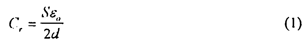
- S is the size of the top face (the face closest to the skin surface 18) of each capacitor plate 23, 24 of capacitors 33, 34
- ⁇ o is the electric constant (seeing as, in the fingerprinting application, the average distance between the skin surface 18 and the insul
- the variation in output voltage as a result of the charge step is directly proportional to the distance between the capacitor plates 23, 24 and the skin surface 18, in turn dependent on the three-dimensional structure of the skin.
- the output voltage of the inverter 30 will range between two extremes, depending on feedback capacitance value: (i) the upper saturation level if no feedback capacitance is present; (ii) a value close to the logical threshold when the feedback capacitance is large.
- the output signals of the device according to the invention are therefore such, when converted into grey levels, as to provide a highly reliable representation of the three-dimensional structure of the skin surface.
- FIG 4 is an illustration of the skin surface 18 positioned on first and second adjacent cells 2A, 2B of the sensor device 1. It is to be understood that the present invention will have application to thumbs, palms, and any contact surface where an image is desired.
- Each of the adjacent cells 2A, 2B is substantially identical to the cell 2 shown in Figures 2-3, and thus, additional detailed discussions of the elements of cells 2A, 2B are being omitted for simplicity.
- Switches 19A and 19B constitute reset switches, as explained in more detail elsewhere herein.
- the elements of the adjacent cells 2A, 2B are marked with labels corresponding to the labels of Figures 2 and 3 with an "A" and a "B" added to the cells 2A and 2B, respectively.
- the skin surface 18 shown in Figure 4 includes a ridge 36 adjacent to the first cell 2A and a valley 38 adjacent to the second cell 2B.
- the first and second cells 2A, 2B will each produce different capacitive coupling responses in the sensor device 1.
- the first cell 2A will sense a smaller distance d1, signifying the ridge 36, than the second cell 2B, which senses a larger distance d2, signifying the valley 38.
- the distance d2 sensed by the second cell 2B will be the average of a distance d2a between the first capacitor plate 23B and the portion of the skin surface 18 directly above the first capacitor plate 23B and a distance d2b between the second capacitor plate 24B and the portion of the skin surface 18 directly above the second capacitor plate 24B. From a lumped-model point of view, this structure realizes a three-capacitor scheme that can sense the difference between a contacting member, a ridge, and a non-contacting member, a valley.
- the sensor device 1 includes the sensor array 3 which is coupled by a digital to analog (D/A) converter 40 to an I 2 C interface and control device 42 and a bias generator 44.
- D/A digital to analog
- the sensor device 1 also includes an oscillator 46 and timing generator 48 coupled to the sensor array 3.
- the D/A converter 40, I 2 C interface and control device 42, bias generator 44, oscillator 46, and timing generator 48 together implement the functionality of the supply and logic unit 7 discussed above.
- the I 2 C interface and control device 42 provides a bidirectional communication protocol that enables the sensor device 1 to communicate with a controller, such as a standard computer.
- the D/A converter 40 converts digital control signals from the I 2 C interface and control device 42 into analog signals that are transmitted to the sensor array 3 to control the scanning of the cells 2 by the horizontal and vertical scanners 5,6.
- the D/A converter 42 also provides analog biases, such as the voltage step V .
- the timing generator 48 takes a single clock signal from the oscillator 46 and generates timing signals that are provided to the sensor array 3 under the control of the I 2 C interface and control device 42.
- the sensor device includes an analog to digital (A/D) converter 50 coupled between the output 10 of the sensor array 3 and the computer.
- the A/D converter 50 also is coupled to the bias generator 44 and timing generator 48 to enable the A/D converter 50 to convert the analog voltage measurements output by the sensor array 3 to digital signals that are recognized by the computer as distance measurements.
- the sensor array 3 also is directly coupled to the computer by a synchronization line 52 that provides the computer with synchronization signals that help the computer properly interpret the digital distance measurements received from the A/D converter 50.
- the cell 2 includes first and second transistors M1, M2 of the N-channel type and third and fourth transistors M3, M4 of the P-channel type connected together in series to comprise a high gain cascode inverting amplifier 13.
- a first horizontal scan line (hor1) and a first vertical scan line (vert1) are coupled respectively from the horizontal and vertical scanners 5, 6 to the second transistor M2 and the third transistor M3 to ensure that only one cell at a time is powered, thereby limiting power consumption of non-addressed cells.
- a gate terminal of the first transistor M1 is coupled by the input capacitor 20 of the cell 2 to the cell input 21. ⁇ V r , as discussed above.
- a charge amount dQ C i ⁇ V r is sinked from the amplifier input 16 as previously explained.
- This mode of operation is useful since by changing the amount of ⁇ V r , the sensor can deal with different ranges of sensed capacitances.
- the gate of the fourth transistor M4 is coupled to a fixed bias V p .
- the output 17 of the inverting amplifier 13 is buffered by a source follower stage (fifth transistor M5) into a vertical output line 54 by means of a sixth transistor M6.
- a seventh transistor M7 couples the vertical output line 54 to the output buffer 8 of the sensor device 1.
- the gate of the sixth transistor M6 is coupled by a second horizontal scan line (hor2) to the horizontal scanner 5 and the gate of the seventh transistor M7 is coupled by a second vertical scan line (vert2) to the vertical scanner 6, which ensures that only one cell at a time is communicating with the output buffer 8. This greatly reduces the output capacitance of the follower stage 46 since only one vertical output line at a time is connected to the output buffer 8.
- the reset switch 19 is connected between the input 16 and output 17 of the inverting amplifier 13 as discussed above.
- the reset switch 19 is designed to prevent charge injection in the input 16 from saturating the inverting amplifier 13. If the switch-off transient of the reset switch 19 is slow enough compared to the inverse of the gain bandwidth product of the inverting amplifier 13, most of the channel charge of the reset switch is injected into the output node.
- the reset switch 19 includes eighth and ninth transistors M8, M9 with their drain terminals coupled together to the input 16 and their source terminals coupled together to the output 17. The size of the eighth transistor M8 is small in order to reduce the absolute amount of injected charge.
- the ninth transistor M9 is stronger than the eighth transistor M8 and is activated at a different phase than the eighth transistor M8 is introduced. During the reset phase, both transistors M8, M9 are set, reducing resistance of the feedback loop so output ringing is contained. During charge integration, the ninth transistor M9 is first opened so its channel charge is absorbed by the eighth transistor M8. Finally, the eighth transistor M8 is opened by a slow gate transient to ensure low charge-injection on the input. It will be appreciated that the ninth transistor M9 is optional because charge injection is less of an issue if the plate capacities are bigger.
- the chip is made using a 0.7 ⁇ m CMOS digital process.
- the cell area is 50 x 50 ⁇ m 2 , giving a 508 dpi resolution.
- a sample image 56 produced for a 200 x 200 window is shown in Figure 7, which clearly shows grey levels. The image disappears as the finger is removed.
- the sensitivity of the individual sensor cells 2, and thus the entire sensor device 1, can be controlled and enhanced by arranging the first and second capacitor plates 23, 24 in one or more planar patterns.
- a first pattern of the capacitor plates 23, 24 is shown in Figure 8.
- the first capacitor plate 23 is C-shaped and has two ends 60, 62 that define a gap 64 therebetween.
- the first capacitor plate 23 includes elongated first, second, and third segments 66, 68, 70 that define three sides of the C-shape and shorter fourth and fifth segments 72, 74 that terminate in the first and second ends 60, 62 on a fourth side of the C-shape.
- the five segments 66-74 of the first capacitor plate 23 together define an inner area 76 within which is positioned a rectangular inner portion 78 of the second capacitor plate 24.
- the second capacitor plate 24 also includes an elongated, rectangular outer portion 80 outside of the first capacitor plate and a connector portion 82 that connects the inner portion 78 with the outer portion 80.
- the first capacitor plate 23 includes several faces that are adjacent to and face corresponding faces of the second capacitor plate 24 which allows fringing capacitances to be developed between the capacitor plates.
- the first capacitor plate 23 has first and second faces 83, 84 that face respective first and second faces 85, 86 of the second capacitor plate 24.
- the first and second capacitor plates 23, 24 respectively include upper faces 87, 88 that face the object being sensed and allowed first and second direct capacitances to develop between the object and the first and second capacitor plates, respectively.
- ground ring 89 Completely surrounding the sensor cell 2 is a ground ring 89 that is connected to ground to provide a discharge path for any electrostatic discharge that is caused by the object being sensed.
- the finger may produce an electrostatic discharge as it approaches the sensor cell, which would produce an erroneous distance measurement if allowed to discharge through one of the capacitor plates 23, 24.
- the ground ring 89 is a metal pattern layer that can be deposited according to well-known techniques as part of an integrated circuit that includes the elements shown in Figure 2.
- the ground ring 89 is separated electrically and physically from the capacitor plates 23, 24 by a first passivation layer 90 that also physically separates and electrically insulates the first capacitor plate 23 from the second capacitor plate 24.
- the first passivation layer 90 can be composed of many known dielectric materials, such as phosphorous doped glass (PSG), silicon dioxide, silicon nitride, and silicon oxynitride.
- a second passivation layer (not shown in Figure 8) is deposited on the capacitor plates 23, 24, ground ring 89, and first passivation layer 90 and acts as the dielectric insulating layer 25 shown in Figures 2 and 4.
- the average distance between the first and second capacitor plates 23, 24 and the embodiment shown in Figure 8 generally is between 0.5 and 4 ⁇ m which is similar to the typical thickness of the insulating layer 25.
- the total feedback capacitance experienced by the inverter amplifier 13 ( Figure 2) is composed of a first direct capacitance between the first capacitor plate 23 and the object, a second direct capacitance between the second capacitor plate 24 and the object, and a fringing capacitance between the first capacitor plate 23 and the second capacitor plate 24.
- the first and second direct capacitances vary according to the respective areas of the upper faces of the first and second capacitor plates 23, 24 as described in Equation 1. As such, increasing the areas of the capacitor plates 23, 24 increases the total capacitance, which provides more sensitivity and a greater dynamic range for the sensor device 1.
- the fringing capacitance varies according to the perimeter values for the first and second capacitor plates 23, 24, that is, a total length of the perimeters of the capacitor plates.
- the widths of the top surfaces of the capacitor plates 23, 24 generally is an order of magnitude greater than the depth of the sides of the capacitor plates, and thus, the direct capacitances generally contribute more to the total capacitance than the fringing capacitance.
- a second embodiment of the sensor cell 2 is shown in Figure 9.
- the first capacitor plate 23 has several fingers 91 that are interdigitated with fingers 92 of the second capacitor plate 24.
- a first connecting segment 93 connects the fingers 91 of the first capacitor plate to each other and a second connecting segment 94 connects the fingers 92 of the second capacitor plate to each other.
- the first capacitor plate 23 is separated from the second capacitor plate 24 and from the ground ring 89 by the first passivation layer 90.
- the first capacitor plate 23 has several faces that face corresponding faces of the first capacitor plate. As can be seen, the total perimeter for the capacitor plates 23, 24 in the pattern shown in Figure 9 is greater than the total perimeter of the capacitor plates 23, 24 in the pattern shown in Figure 8.
- the interdigitated pattern shown in Figure 9 likely will have greater fringing capacitance than the pattern shown in Figure 8.
- the interdigitated pattern of Figure 9 will have a greater sensitivity to smaller objects, such as water vapor, than the pattern of Figure 8.
- the pattern of Figure 8 generally will be more robust and cost less than the interdigitated pattern of Figure 9 because of the complicated nature of the interdigitated pattern.
- a third embodiment of the sensor cell 2 is shown in Figure 10.
- the first capacitor plate 23 includes two rectangular portions 96, 98 positioned in diagonally opposite first and second sections of the sensor cell 2 and are connected by a connector portion 100.
- the second capacitor plate also includes two rectangular portions 102, 104 positioned in diagonally opposite third and fourth sections of the sensor cell 2 and are connected by a second connector portion 106.
- one of the connector portions 100, 106 is positioned in a lower metal layer than the other connector portion with a passivation layer (not shown) electrically insulating the two connector portions.
- the first capacitor plate 23 is separated from the second capacitor plate 24 and from the ground ring 89 by the first passivation layer 90.
- each capacitor plate 23, 24 is approximately 441 ⁇ m 2 , for a total capacitor area of 882 ⁇ m 2 .
- a fourth embodiment of the sensor cell 2 is shown in Figure 11.
- the first capacitor plate 23 includes five fingers 108 extending outwardly from a central portion 110.
- the first capacitor plate 23 is coplaner with and completely surrounded by the second capacitor plate 24.
- the second capacitor plate 24 also includes five fingers 112 that interdigitate with the five fingers 108 of the first capacitor plate 23.
- the first capacitor plate 23 is separated from the second capacitor plate 24 and from the ground ring 89 by the first the passivation layer 90.
- the patterns shown in Figures 10 and 11 have smaller total perimeters and the total perimeter of the interdigitated pattern of Figure 9, and thus, likely would be less sensitive to objects smaller than the sensor cell 2, such as water vapor and molecules.
- the patterns of Figures 10 and 11 are easier to make than the pattern of Figure 9 and are more robust and less costly.
- a fifth embodiment of the sensor cell 2 is shown in Figure 12.
- the first and second capacitor plates 23, 24, are arranged in a spiral pattern.
- the first capacitor plate 23 is separated from the second capacitor plate 24 and from the ground ring 89 by the first passivation layer 90.
- the spiral pattern shown in Figure 12 has a greater total perimeter, but a less total area than the capacitor pattern shown in Figures 10 and 11.
- the spiral pattern of Figure 12 likely will be more sensitive to very small objects, such as water vapor, likely will be less sensitive to large objects, such as fingers because its lower total area produces less total capacitance.
- each of the sensor cells 2 is square, although other rectangles and other shapes could be employed depending on the application.
- Each sensor cell, 25 typically will be from an approximately 25 x 25 ⁇ m to approximately 100 x 100 ⁇ m. In one implication, each sensor cell is 50 x 50 ⁇ m which corresponds to a 508 dots per inch (dpi) resolution.
- the ground rings 89 are shared by adjacent sensor cells 2 to produce a grounding element grid 112.
- the grounding element grid 112 includes grounding grid segments 114 between each cell and its immediately adjacent cells. Such a grounding element grid insures that any ESD produced by the object being sensed will be discharged through the grounding element grid directly to ground rather than through the capacitor plates 23, 24.
- Each of the sensor cells 2 of the array 3 can include the same pattern of capacitor plates 23, 24 or plural capacitor patterns could be employed depending on the application.
- Each sensor cell 2 can imply any of the capacitor patterns shown in Figures 8-12 or numerous other capacitor patterns such as fractal patterns and numerous other shapes.
- the sensor cells 2 described above are preferably formed using conventional silicon integrated circuit methodology. More particularly, all of the elements of the sensor device 1 shown in Figures 1-6 can be integrated on a single chip. Alternatively, one or more of the elements, such as the oscillator 46, can be made separately and coupled to the integrated elements of the sensor device 1.
- the sensor device shown in Figures 1-6 and 8-13 has at least the following advantages.
- the sensor device provides for a high degree of precision with no need for complex processing of the output signal.
- the sensor device may be produced easily and integrated using current microelectronic technology and is highly reliable, compact, and cheap to produce.
- the sensor device according to the invention may also be used to advantage in other applications requiring precise detection of small distances.
- each cell enables a large number of cells to be accommodated in array structures for detecting two-dimensional physical quantities.
- inverting amplifier 13 may be connected directly to the input or output of inverting amplifier 13 to eliminate one of capacitor plates 23, 24.
- all the components may be replaced by technical equivalents.
- amplifier 13 may be implemented by any inverting or differential amplifier (e.g ., an operational amplifier) in a charge amplifier configuration to increase the speed of the output signal.
Abstract
Description
Claims (14)
- An integrated sensor device for detecting a distance between the sensor device and an object, the sensor device comprising:a first capacitor plate for forming a first capacitance between the first capacitor plate and the object when positioned adjacent to the object;a second capacitor plate for forming a second capacitance between the second capacitor plate and the object when positioned adjacent to the object, the first and second capacitor plates being arranged in a substantially planar pattern in which a plurality of faces of the first capacitor plate are positioned adjacent to and facing a plurality of faces of the second capacitor plate; andan amplifier having an input and an output, the input being connected to one of the first and second capacitor plates and the output being connected to another one of the first and second capacitor plates to form a negative feedback branch that includes the first and second capacitances, whereby an output voltage is established at the amplifier output that is proportional to a distance between the first capacitor plate and the object.
- The sensor device of claim 1, further comprising a layer of insulating material contacting outer surfaces of the first and second capacitor plates, such that the insulating material is positioned between the capacitor plates and the object.
- The sensor device of claim 1, further comprising:a grounding element surrounding the first and second capacitor plates in a plane, the grounding element being coupled to ground to provide a discharge path for electrostatic discharge caused by the object.
- The sensor device of claim 1 wherein the first and second capacitor plates are arranged in an interdigitating pattern in which fingers of the first capacitor plate are interspersed with fingers of the second capacitor plate.
- The sensor device of claim 1 wherein the first capacitor plate is C-shaped and has two ends that define a gap and the second capacitor place includes an inner portion surrounded on at least three sides by the first capacitor plate, an outer portion positioned outside the first capacitor plate and a connector portion connecting the inner portion with the outer portion.
- The sensor device of claim 1 wherein the first capacitor plate includes two rectangular portions positioned in diagonally opposite sections of a rectangular sensor cell and a connector portion that connects the two rectangular portions and the second capacitor plate includes two rectangular portions positioned in diagonally opposite sections of the rectangular sensor cell and a connector portion that connects the two rectangular portions of the second capacitor plate and crosses the connector portion of the first capacitor plate.
- A sensor device comprising:an array of distance detecting cells for detecting a distance between an object and the sensor device, wherein the cells each comprise a capacitive distance sensor that includes a first capacitor plate positioned facing the object and thereby defining a capacitive element indicative of the distance being detected therebetween; andone or more grounding elements positioned between the cells of the array, each cell having one or more of the grounding elements positioned between the cell and one or more adjacent cells, each grounding element being coupled to ground to provide a discharge path for electrostatic discharge.
- The sensor device of claim 7 wherein the one or more grounding elements includes a grounding element grid that includes grounding grid segments between each cell and its immediately adjacent cells.
- The sensor device of claim 7 wherein each cell further includes a second capacitor plate and the first and second capacitor plates are arranged in an interdigitating pattern in which fingers of the first capacitor plate are interspersed with fingers of the second capacitor plate.
- The sensor device of claim 4 or claim 9 wherein the first capacitor plate surrounds the second capacitor plate in a plane.
- The sensor device of claim 1 or claim 7 wherein first and second capacitor plates are arranged in a spiral pattern.
- The sensor device of claim 7 wherein each cell further includes a second capacitor plate and the first capacitor plate is C-shaped and has two ends that define a gap and the second capacitor plate includes an inner portion surrounded on at least three sides by the first capacitor plate, an outer portion positioned outside the first capacitor plate, and a connector portion connecting the inner portion with the outer portion.
- The sensor device of claim 7 wherein the first capacitor plate of each cell includes two rectangular portions positioned in diagonally opposite sections of the cell and a connector portion that connects the two rectangular portions and each cell further includes a second capacitor plate that includes two rectangular portions positioned in diagonally opposite sections of the rectangular sensor cell and a connector portion that connects the two rectangular portions of the second capacitor plate and crosses the connector portion of the first capacitor plate.
- A method of making a capacitive distance sensor for detecting a distance between the sensor and an object, the sensor including one or more sensor cells each with first and second capacitor plates, the method comprising:determining an expected range of sizes of the object the sensor will be used to detect;determining a total perimeter value for each of a plurality of capacitor patterns, each capacitor pattern including a different arrangement of the first and second capacitor plates, the total perimeter value being the sum of perimeter values for the first and second capacitor plates;selecting a capacitor pattern from among a plurality of capacitor patterns based on the expected size of the object and on the total perimeter values determined for the plurality of capacitor patterns, the selecting step including selecting whichever one of the plurality of capacitor patterns has the largest total perimeter value if the object the sensor will be used to detect is smaller than each of the one or more sensor cells; andforming the selected capacitor pattern in at least one of the one or more sensor cells.
Applications Claiming Priority (2)
| Application Number | Priority Date | Filing Date | Title |
|---|---|---|---|
| US40261 | 1998-03-09 | ||
| US09/040,261 US6114862A (en) | 1996-02-14 | 1998-03-09 | Capacitive distance sensor |
Publications (2)
| Publication Number | Publication Date |
|---|---|
| EP0942259A1 true EP0942259A1 (en) | 1999-09-15 |
| EP0942259B1 EP0942259B1 (en) | 2004-11-10 |
Family
ID=21910024
Family Applications (1)
| Application Number | Title | Priority Date | Filing Date |
|---|---|---|---|
| EP99301681A Expired - Lifetime EP0942259B1 (en) | 1998-03-09 | 1999-03-05 | Capacitive distance sensor |
Country Status (4)
| Country | Link |
|---|---|
| US (3) | US6114862A (en) |
| EP (1) | EP0942259B1 (en) |
| JP (1) | JPH11316105A (en) |
| DE (1) | DE69921712T2 (en) |
Cited By (13)
| Publication number | Priority date | Publication date | Assignee | Title |
|---|---|---|---|---|
| DE19949922C1 (en) * | 1999-10-16 | 2001-05-31 | Sita Messtechnik Gmbh | Method and device for measuring the foam properties of liquids |
| EP1113383A2 (en) * | 1999-12-30 | 2001-07-04 | STMicroelectronics, Inc. | Enhanced fingerprint detection |
| DE19954567C1 (en) * | 1999-11-12 | 2001-08-02 | Infineon Technologies Ag | Positioning arrangement |
| EP1178536A2 (en) * | 2000-08-03 | 2002-02-06 | Casio Computer Co., Ltd. | Image reading apparatus |
| WO2002099731A1 (en) * | 2001-06-01 | 2002-12-12 | Infineon Technologies Ag | Biometric sensor |
| WO2002100770A2 (en) * | 2001-06-08 | 2002-12-19 | Siemens Aktiengesellschaft | Wafer assembly and a method for producing a wafer assembly |
| DE10133363A1 (en) * | 2001-07-10 | 2003-01-30 | Infineon Technologies Ag | Measuring cell and measuring field with such measuring cells as well as using a measuring cell and using a measuring field |
| CN101493738B (en) * | 2008-01-25 | 2011-01-12 | 原相科技股份有限公司 | Method for detecting pressure action of user and optical manipulation unit |
| CN102681737A (en) * | 2011-02-28 | 2012-09-19 | 宸鸿光电科技股份有限公司 | A capacitive touch panel and a method for manufacturing the capacitive touch panel |
| WO2015134164A1 (en) * | 2014-03-04 | 2015-09-11 | Apple Inc. | Field shaping channels in a substrate above a biometric sensing device |
| EP3249573A4 (en) * | 2015-01-19 | 2018-08-15 | Boe Technology Group Co. Ltd. | Fingerprint recognition device and touch apparatus |
| US10372965B2 (en) | 2015-06-22 | 2019-08-06 | Nxp B.V. | Fingerprint sensing system |
| WO2023167766A3 (en) * | 2022-02-01 | 2023-11-23 | Georgia Tech Research Corporation | Active biosensing electrode and method |
Families Citing this family (157)
| Publication number | Priority date | Publication date | Assignee | Title |
|---|---|---|---|---|
| US6114862A (en) | 1996-02-14 | 2000-09-05 | Stmicroelectronics, Inc. | Capacitive distance sensor |
| EP0790479B1 (en) | 1996-02-14 | 2002-01-16 | STMicroelectronics S.r.l. | Capacitive distance sensor, particularly for acquiring fingerprints |
| US6320394B1 (en) | 1996-02-14 | 2001-11-20 | Stmicroelectronics S.R.L. | Capacitive distance sensor |
| US6483931B2 (en) | 1997-09-11 | 2002-11-19 | Stmicroelectronics, Inc. | Electrostatic discharge protection of a capacitve type fingerprint sensing array |
| US6317508B1 (en) * | 1998-01-13 | 2001-11-13 | Stmicroelectronics, Inc. | Scanning capacitive semiconductor fingerprint detector |
| US6091082A (en) | 1998-02-17 | 2000-07-18 | Stmicroelectronics, Inc. | Electrostatic discharge protection for integrated circuit sensor passivation |
| EP0940652B1 (en) * | 1998-03-05 | 2004-12-22 | Nippon Telegraph and Telephone Corporation | Surface shape recognition sensor and method of fabricating the same |
| KR100703140B1 (en) | 1998-04-08 | 2007-04-05 | 이리다임 디스플레이 코포레이션 | Interferometric modulation and its manufacturing method |
| US8928967B2 (en) * | 1998-04-08 | 2015-01-06 | Qualcomm Mems Technologies, Inc. | Method and device for modulating light |
| DE19833211C2 (en) * | 1998-07-23 | 2000-05-31 | Siemens Ag | Method for determining very small capacities and use |
| US6686546B2 (en) * | 1998-12-30 | 2004-02-03 | Stmicroelectronics, Inc. | Static charge dissipation for an active circuit surface |
| US6346739B1 (en) * | 1998-12-30 | 2002-02-12 | Stmicroelectronics, Inc. | Static charge dissipation pads for sensors |
| US6440814B1 (en) | 1998-12-30 | 2002-08-27 | Stmicroelectronics, Inc. | Electrostatic discharge protection for sensors |
| US6478976B1 (en) | 1998-12-30 | 2002-11-12 | Stmicroelectronics, Inc. | Apparatus and method for contacting a conductive layer |
| US6326227B1 (en) * | 1998-12-30 | 2001-12-04 | Stmicroelectronics, Inc. | Topographical electrostatic protection grid for sensors |
| US6330145B1 (en) | 1998-12-30 | 2001-12-11 | Stmicroelectronics, Inc. | Apparatus and method for contacting a sensor conductive layer |
| DE19901384A1 (en) * | 1999-01-15 | 2000-07-27 | Siemens Ag | Electronic component and use of a protective structure contained therein |
| DE60032286T8 (en) * | 1999-06-10 | 2007-09-27 | Nippon Telegraph And Telephone Corp. | Device for recognizing surface shapes |
| US6423995B1 (en) * | 1999-07-26 | 2002-07-23 | Stmicroelectronics, Inc. | Scratch protection for direct contact sensors |
| ATE444709T1 (en) * | 1999-08-09 | 2009-10-15 | Sonavation Inc | PIEZOELECTRIC THIN FILM FINGERPRINT SCANNER |
| JP4233698B2 (en) * | 1999-08-12 | 2009-03-04 | セイコーインスツル株式会社 | Fingerprint reading apparatus and method |
| WO2003007049A1 (en) * | 1999-10-05 | 2003-01-23 | Iridigm Display Corporation | Photonic mems and structures |
| US6448790B1 (en) * | 1999-10-26 | 2002-09-10 | Citizen Watch Co., Ltd. | Electrostatic capacitance detecting device |
| DE29920733U1 (en) * | 1999-11-26 | 2001-04-05 | Platz Karl Otto | Capacitive sensors based on glass |
| US7239227B1 (en) | 1999-12-30 | 2007-07-03 | Upek, Inc. | Command interface using fingerprint sensor input system |
| US6512381B2 (en) | 1999-12-30 | 2003-01-28 | Stmicroelectronics, Inc. | Enhanced fingerprint detection |
| US20030098774A1 (en) * | 2000-03-21 | 2003-05-29 | Chornenky Todd E. | Security apparatus |
| US6943665B2 (en) | 2000-03-21 | 2005-09-13 | T. Eric Chornenky | Human machine interface |
| US7067962B2 (en) | 2000-03-23 | 2006-06-27 | Cross Match Technologies, Inc. | Multiplexer for a piezo ceramic identification device |
| US20030001459A1 (en) * | 2000-03-23 | 2003-01-02 | Cross Match Technologies, Inc. | Secure wireless sales transaction using print information to verify a purchaser's identity |
| JP2003527906A (en) * | 2000-03-23 | 2003-09-24 | クロス マッチ テクノロジーズ, インコーポレイテッド | Piezoelectric identification device and its application |
| JP2001330634A (en) * | 2000-05-23 | 2001-11-30 | Konica Corp | Capacitance measuring method and device therefor |
| US6501284B1 (en) * | 2000-08-28 | 2002-12-31 | Stmicroelectronics, Inc. | Capacitive finger detection for fingerprint sensor |
| JP4201476B2 (en) * | 2000-10-13 | 2008-12-24 | 富士通株式会社 | Fingerprint recognition device |
| US6552667B1 (en) * | 2000-11-16 | 2003-04-22 | Hydro-Quebec | Non-contact measuring method and apparatus for producing a signal representative of a distance between facing surfaces |
| US6715089B2 (en) * | 2001-01-22 | 2004-03-30 | Ati International Srl | Reducing power consumption by estimating engine load and reducing engine clock speed |
| US6525547B2 (en) * | 2001-04-17 | 2003-02-25 | Sentronics Corporation | Capacitive two dimensional sensor |
| WO2002089038A2 (en) * | 2001-04-27 | 2002-11-07 | Atrua Technologies, Inc. | Capacitive sensor system with improved capacitance measuring sensitivity |
| US6515488B1 (en) | 2001-05-07 | 2003-02-04 | Stmicroelectronics, Inc. | Fingerprint detector with scratch resistant surface and embedded ESD protection grid |
| KR100393191B1 (en) * | 2001-05-12 | 2003-07-31 | 삼성전자주식회사 | Fingerprint sensor using piezoelectric membrane |
| EP1407477A4 (en) * | 2001-05-22 | 2006-06-07 | Atrua Technologies Inc | Improved connection assembly for integrated circuit sensors |
| US7259573B2 (en) * | 2001-05-22 | 2007-08-21 | Atrua Technologies, Inc. | Surface capacitance sensor system using buried stimulus electrode |
| US20020192653A1 (en) * | 2001-06-13 | 2002-12-19 | Stetter Joseph Robert | Impedance-based chemical and biological imaging sensor apparatus and methods |
| US6545486B2 (en) * | 2001-08-30 | 2003-04-08 | Stmicroelectronics, Inc. | Solution and methodology for detecting surface damage on capacitive sensor integrated circuit |
| US6661410B2 (en) | 2001-09-07 | 2003-12-09 | Microsoft Corporation | Capacitive sensing and data input device power management |
| US6636053B1 (en) | 2001-11-02 | 2003-10-21 | Stmicroelectronics, Inc. | Capacitive pixel for fingerprint sensor |
| US6927581B2 (en) * | 2001-11-27 | 2005-08-09 | Upek, Inc. | Sensing element arrangement for a fingerprint sensor |
| US6707093B2 (en) | 2001-11-30 | 2004-03-16 | Stmicroelectronics, Inc. | Selective ionic implantation of fluoropolymer film to modify the sensitivity of underlying sensing capacitors |
| US6693441B2 (en) | 2001-11-30 | 2004-02-17 | Stmicroelectronics, Inc. | Capacitive fingerprint sensor with protective coating containing a conductive suspension |
| US6762470B2 (en) | 2001-11-30 | 2004-07-13 | Stmicroelectronics, Inc. | Fingerprint sensor having a portion of the fluorocarbon polymer physical interface layer amorphized |
| US20030104693A1 (en) * | 2001-11-30 | 2003-06-05 | Siegel Harry M. | Use of fluoropolymer coating for planarizing and passivating integrated circuit devices |
| JP3980387B2 (en) * | 2002-03-20 | 2007-09-26 | 富士通株式会社 | Capacitance detection type sensor and manufacturing method thereof |
| US6852996B2 (en) * | 2002-09-25 | 2005-02-08 | Stmicroelectronics, Inc. | Organic semiconductor sensor device |
| US20040125990A1 (en) * | 2002-12-26 | 2004-07-01 | Motorola, Inc. | Method and apparatus for asperity detection |
| EP1445577A1 (en) * | 2003-01-30 | 2004-08-11 | ALSTOM Technology Ltd | A method and an apparatus for determining the distance between a collimator lens and an object |
| EP2604216B1 (en) | 2003-02-25 | 2018-08-22 | Tria Beauty, Inc. | Self-contained, diode-laser-based dermatologic treatment apparatus |
| US8709003B2 (en) * | 2003-02-25 | 2014-04-29 | Tria Beauty, Inc. | Capacitive sensing method and device for detecting skin |
| US6900644B2 (en) * | 2003-05-06 | 2005-05-31 | Ligh Tuning Tech. Inc. | Capacitive fingerprint sensor against ESD damage and contamination interference |
| GB0310409D0 (en) * | 2003-05-07 | 2003-06-11 | Koninkl Philips Electronics Nv | Object sensing |
| US6906529B2 (en) * | 2003-06-10 | 2005-06-14 | Stmicroelectronics, Inc. | Capacitive sensor device with electrically configurable pixels |
| JP4517599B2 (en) * | 2003-08-19 | 2010-08-04 | セイコーエプソン株式会社 | Capacitance detection device |
| JP4539044B2 (en) * | 2003-08-29 | 2010-09-08 | セイコーエプソン株式会社 | Capacitance detection device |
| US20080297878A1 (en) * | 2003-10-01 | 2008-12-04 | Board Of Regents, The University Of Texas System | Compositions, methods and systems for making and using electronic paper |
| US20050079386A1 (en) * | 2003-10-01 | 2005-04-14 | Board Of Regents, The University Of Texas System | Compositions, methods and systems for making and using electronic paper |
| US8665325B2 (en) | 2003-10-08 | 2014-03-04 | Qwest Communications International Inc. | Systems and methods for location based image telegraphy |
| TWI226934B (en) * | 2003-11-27 | 2005-01-21 | Hong Hocheng | System of nanoimprint with mold deformation detector and method of monitoring the same |
| US20060009749A1 (en) * | 2004-02-19 | 2006-01-12 | Weckwerth Mark V | Efficient diffuse light source assembly and method |
| US8777935B2 (en) * | 2004-02-25 | 2014-07-15 | Tria Beauty, Inc. | Optical sensor and method for identifying the presence of skin |
| US7071708B2 (en) * | 2004-04-16 | 2006-07-04 | Lightuning Tech. Inc. | Chip-type sensor against ESD and stress damages and contamination interference |
| US6970031B1 (en) | 2004-05-28 | 2005-11-29 | Hewlett-Packard Development Company, L.P. | Method and apparatus for reducing charge injection in control of MEMS electrostatic actuator array |
| TW200611287A (en) * | 2004-09-24 | 2006-04-01 | Holtek Semiconductor Inc | Capacitance induction device |
| US7420725B2 (en) | 2004-09-27 | 2008-09-02 | Idc, Llc | Device having a conductive light absorbing mask and method for fabricating same |
| US7944599B2 (en) | 2004-09-27 | 2011-05-17 | Qualcomm Mems Technologies, Inc. | Electromechanical device with optical function separated from mechanical and electrical function |
| US7564612B2 (en) | 2004-09-27 | 2009-07-21 | Idc, Llc | Photonic MEMS and structures |
| US7289259B2 (en) | 2004-09-27 | 2007-10-30 | Idc, Llc | Conductive bus structure for interferometric modulator array |
| US7372613B2 (en) | 2004-09-27 | 2008-05-13 | Idc, Llc | Method and device for multistate interferometric light modulation |
| JP4481806B2 (en) * | 2004-12-03 | 2010-06-16 | アルプス電気株式会社 | Capacitance detection type sensor |
| US7433167B2 (en) * | 2005-03-08 | 2008-10-07 | Synaptics Incorporated | Strike ring based electrostatic discharge protection |
| US7227293B2 (en) * | 2005-05-11 | 2007-06-05 | Tai-Saw Technology Co., Ltd. | Surface acoustic wave device with electro-static discharge protection |
| TWI310521B (en) * | 2005-06-29 | 2009-06-01 | Egis Technology Inc | Structure of sweep-type fingerprint sensing chip capable of resisting electrostatic discharge (esd) and method of fabricating the same |
| WO2007013011A1 (en) * | 2005-07-28 | 2007-02-01 | Koninklijke Philips Electronics N.V. | Object sensing system |
| US7738681B1 (en) | 2005-11-01 | 2010-06-15 | Hewlett-Packard Development Company, L.P. | Fingerprint and physical attribute detection |
| US7547572B2 (en) * | 2005-11-16 | 2009-06-16 | Emcore Corporation | Method of protecting semiconductor chips from mechanical and ESD damage during handling |
| US7916980B2 (en) | 2006-01-13 | 2011-03-29 | Qualcomm Mems Technologies, Inc. | Interconnect structure for MEMS device |
| US20070175322A1 (en) * | 2006-02-02 | 2007-08-02 | Xpresense Llc | RF-based dynamic remote control device based on generating and sensing of electrical field in vicinity of the operator |
| TW200737486A (en) * | 2006-03-24 | 2007-10-01 | Lightuning Tech Inc | Semiconductor integrated circuit chip with nano-structure-surface resin passivation and method of fabricating the same |
| US7649671B2 (en) | 2006-06-01 | 2010-01-19 | Qualcomm Mems Technologies, Inc. | Analog interferometric modulator device with electrostatic actuation and release |
| JP4828316B2 (en) * | 2006-06-13 | 2011-11-30 | 三菱電機株式会社 | GAP DETECTING DEVICE, LASER PROCESSING SYSTEM, AND GAP DETECTING METHOD FOR LASER MACHINE |
| US7527998B2 (en) | 2006-06-30 | 2009-05-05 | Qualcomm Mems Technologies, Inc. | Method of manufacturing MEMS devices providing air gap control |
| US7545621B2 (en) * | 2006-07-24 | 2009-06-09 | Yt Acquisition Corporation | Electrostatic discharge structure for a biometric sensor |
| CH698425B1 (en) * | 2006-12-01 | 2009-08-14 | Hsr Hochschule Fuer Technik Ra | System for measuring a physical quantity. |
| US8115987B2 (en) | 2007-02-01 | 2012-02-14 | Qualcomm Mems Technologies, Inc. | Modulating the intensity of light from an interferometric reflector |
| TW200842681A (en) | 2007-04-27 | 2008-11-01 | Tpk Touch Solutions Inc | Touch pattern structure of a capacitive touch panel |
| US7643202B2 (en) | 2007-05-09 | 2010-01-05 | Qualcomm Mems Technologies, Inc. | Microelectromechanical system having a dielectric movable membrane and a mirror |
| US7630121B2 (en) | 2007-07-02 | 2009-12-08 | Qualcomm Mems Technologies, Inc. | Electromechanical device with optical function separated from mechanical and electrical function |
| JP2009054993A (en) | 2007-08-02 | 2009-03-12 | Tokyo Electron Ltd | Tool for detecting position |
| US8605050B2 (en) | 2007-08-21 | 2013-12-10 | Tpk Touch Solutions (Xiamen) Inc. | Conductor pattern structure of capacitive touch panel |
| CN101802678B (en) * | 2007-09-17 | 2014-03-12 | 高通Mems科技公司 | Semi-transparent/ transflective lighted interferometric devices |
| US8050467B2 (en) * | 2007-09-19 | 2011-11-01 | Chipbond Technology Corporation | Package, packaging method and substrate thereof for sliding type thin fingerprint sensor |
| US8115497B2 (en) * | 2007-11-13 | 2012-02-14 | Authentec, Inc. | Pixel sensing circuit with common mode cancellation |
| US8941631B2 (en) | 2007-11-16 | 2015-01-27 | Qualcomm Mems Technologies, Inc. | Simultaneous light collection and illumination on an active display |
| TWI374379B (en) | 2007-12-24 | 2012-10-11 | Wintek Corp | Transparent capacitive touch panel and manufacturing method thereof |
| KR101427586B1 (en) * | 2007-12-26 | 2014-08-07 | 삼성디스플레이 주식회사 | Display device and driving method thereof |
| US8073204B2 (en) | 2007-12-31 | 2011-12-06 | Authentec, Inc. | Hybrid multi-sensor biometric identification device |
| EP2252927A4 (en) * | 2008-01-27 | 2011-11-09 | Oxbridge Creation Ltd | Finger-sensing apparatus and method |
| US8164821B2 (en) | 2008-02-22 | 2012-04-24 | Qualcomm Mems Technologies, Inc. | Microelectromechanical device with thermal expansion balancing layer or stiffening layer |
| US7944604B2 (en) | 2008-03-07 | 2011-05-17 | Qualcomm Mems Technologies, Inc. | Interferometric modulator in transmission mode |
| DE112009000941T5 (en) * | 2008-04-15 | 2011-05-26 | Mattel, Inc., El Segundo | Remote control device with touch screen for use with a toy |
| US9687671B2 (en) | 2008-04-25 | 2017-06-27 | Channel Investments, Llc | Optical sensor and method for identifying the presence of skin and the pigmentation of skin |
| US20100045630A1 (en) * | 2008-08-19 | 2010-02-25 | Qualcomm Incorporated | Capacitive MEMS-Based Display with Touch Position Sensing |
| US8358266B2 (en) | 2008-09-02 | 2013-01-22 | Qualcomm Mems Technologies, Inc. | Light turning device with prismatic light turning features |
| US8716778B2 (en) * | 2008-11-17 | 2014-05-06 | Altera Corporation | Metal-insulator-metal capacitors |
| CN102239069B (en) * | 2008-12-04 | 2014-03-26 | 三菱电机株式会社 | Display input device |
| US20100181847A1 (en) * | 2009-01-22 | 2010-07-22 | Shen-Yu Huang | Method for reducing supply voltage drop in digital circuit block and related layout architecture |
| JP5829206B2 (en) | 2009-03-20 | 2015-12-09 | 宸鴻科技(廈門)有限公司TPK Touch Solutions(Xiamen)Inc. | Capacitive touch circuit pattern and manufacturing method thereof |
| US8270056B2 (en) | 2009-03-23 | 2012-09-18 | Qualcomm Mems Technologies, Inc. | Display device with openings between sub-pixels and method of making same |
| DE102009026488A1 (en) * | 2009-05-26 | 2010-12-02 | Bundesdruckerei Gmbh | Microsystem for detecting predetermined features of securities, security documents or other products |
| WO2010138763A1 (en) | 2009-05-29 | 2010-12-02 | Qualcomm Mems Technologies, Inc. | Illumination devices and methods of fabrication thereof |
| TWI447475B (en) * | 2009-09-07 | 2014-08-01 | Au Optronics Corp | Touch panel |
| US8270062B2 (en) | 2009-09-17 | 2012-09-18 | Qualcomm Mems Technologies, Inc. | Display device with at least one movable stop element |
| US8488228B2 (en) | 2009-09-28 | 2013-07-16 | Qualcomm Mems Technologies, Inc. | Interferometric display with interferometric reflector |
| US20110169724A1 (en) * | 2010-01-08 | 2011-07-14 | Qualcomm Mems Technologies, Inc. | Interferometric pixel with patterned mechanical layer |
| CN102834761A (en) | 2010-04-09 | 2012-12-19 | 高通Mems科技公司 | Mechanical layer and methods of forming the same |
| CN103119630B (en) | 2010-07-19 | 2016-11-23 | 里斯特有限公司 | Fingerprint sensor and the system including fingerprint sensor |
| WO2012024238A1 (en) | 2010-08-17 | 2012-02-23 | Qualcomm Mems Technologies, Inc. | Actuation and calibration of a charge neutral electrode in an interferometric display device |
| US9057872B2 (en) | 2010-08-31 | 2015-06-16 | Qualcomm Mems Technologies, Inc. | Dielectric enhanced mirror for IMOD display |
| US20120092279A1 (en) | 2010-10-18 | 2012-04-19 | Qualcomm Mems Technologies, Inc. | Touch sensor with force-actuated switched capacitor |
| US8564314B2 (en) * | 2010-11-02 | 2013-10-22 | Atmel Corporation | Capacitive touch sensor for identifying a fingerprint |
| US8963159B2 (en) | 2011-04-04 | 2015-02-24 | Qualcomm Mems Technologies, Inc. | Pixel via and methods of forming the same |
| US9134527B2 (en) | 2011-04-04 | 2015-09-15 | Qualcomm Mems Technologies, Inc. | Pixel via and methods of forming the same |
| US8659816B2 (en) | 2011-04-25 | 2014-02-25 | Qualcomm Mems Technologies, Inc. | Mechanical layer and methods of making the same |
| US9189675B2 (en) | 2011-04-28 | 2015-11-17 | Moon J. Kim | Adaptive fingerprint scanning |
| US8699762B2 (en) | 2011-05-13 | 2014-04-15 | Moon J. Kim | Multi-sided card having a resistive fingerprint imaging array |
| US8675928B2 (en) | 2011-06-14 | 2014-03-18 | Moon J. Kim | Multiple charge-coupled biometric sensor array |
| CN102866794A (en) | 2011-06-15 | 2013-01-09 | 宸鸿光电科技股份有限公司 | Touch control sensing layer and manufacturing method thereof |
| US8836478B2 (en) * | 2011-09-25 | 2014-09-16 | Authentec, Inc. | Electronic device including finger sensor and related methods |
| US8736939B2 (en) | 2011-11-04 | 2014-05-27 | Qualcomm Mems Technologies, Inc. | Matching layer thin-films for an electromechanical systems reflective display device |
| US9605952B2 (en) | 2012-03-08 | 2017-03-28 | Quality Manufacturing Inc. | Touch sensitive robotic gripper |
| CN107009374A (en) | 2012-03-08 | 2017-08-04 | 品质制造有限公司 | Touch sensitive robot's handgrip |
| CN103327752B (en) * | 2012-03-23 | 2017-12-05 | 富泰华工业(深圳)有限公司 | Clamping device |
| US9024910B2 (en) | 2012-04-23 | 2015-05-05 | Qualcomm Mems Technologies, Inc. | Touchscreen with bridged force-sensitive resistors |
| US9569655B2 (en) * | 2012-04-25 | 2017-02-14 | Jack Harper | Digital voting logic for manufacturable finger asperity wafer-scale solid state palm print scan devices |
| CN104182745B (en) * | 2014-08-15 | 2017-09-22 | 深圳市汇顶科技股份有限公司 | Processing method, system and the fingerprint recognition terminal of fingerprint induced signal |
| US10678381B2 (en) | 2014-08-21 | 2020-06-09 | DISH Technologies L.L.C. | Determining handedness on multi-element capacitive devices |
| US9679128B1 (en) * | 2014-09-22 | 2017-06-13 | Amazon Technologies, Inc. | De-authentication of wearable devices |
| KR101659492B1 (en) * | 2014-11-10 | 2016-09-23 | 한신대학교 산학협력단 | Charge Transfer Circuit for Capacitive Sensing and Apparatus For Detecting Fingerprint Having Thereof |
| US9529433B2 (en) | 2014-12-30 | 2016-12-27 | Stmicroelectronics Pte Ltd | Flexible smart glove |
| US9792482B2 (en) * | 2015-02-27 | 2017-10-17 | Synaptics Incorporated | Multi-mode capacitive sensor |
| TW201638756A (en) * | 2015-04-21 | 2016-11-01 | 映智科技股份有限公司 | Sensing device |
| CN106295473A (en) * | 2015-05-27 | 2017-01-04 | 鸿富锦精密工业(深圳)有限公司 | Fingerprint identification device and there is the electronic installation of this fingerprint identification device |
| US10718359B2 (en) | 2015-08-21 | 2020-07-21 | Quality Manufacturing Inc. | Devices and systems for producing rotational actuation |
| US10089513B2 (en) * | 2016-05-30 | 2018-10-02 | Kyocera Corporation | Wiring board for fingerprint sensor |
| DE102016114188A1 (en) | 2016-08-01 | 2018-02-01 | JENETRIC GmbH | Device and method for direct recording of prints of unrolled fingers |
| RU168950U1 (en) * | 2016-08-03 | 2017-02-28 | Алексей Владимирович Хорват | THICKNESS THICK-FILM DIELECTRIC MATERIALS |
| RU2624660C1 (en) * | 2016-08-03 | 2017-07-05 | Алексей Владимирович Хорват | Thin-film dielectric material thickness control sensor |
| EP3358496B1 (en) * | 2017-02-02 | 2021-04-07 | Nxp B.V. | Fingerprint processing system and method |
| JP7029884B2 (en) * | 2017-04-13 | 2022-03-04 | 株式会社日立製作所 | Humidity detection element and hygrometer |
Citations (6)
| Publication number | Priority date | Publication date | Assignee | Title |
|---|---|---|---|---|
| US4766389A (en) * | 1986-09-03 | 1988-08-23 | Extrude Hone Corporation | Capacitor array sensors tactile and proximity sensing and methods of use thereof |
| US5325442A (en) * | 1990-05-18 | 1994-06-28 | U.S. Philips Corporation | Fingerprint sensing device and recognition system having predetermined electrode activation |
| GB2279756A (en) * | 1990-11-16 | 1995-01-11 | Moonstone Technology Ltd | Device for determining the presence and/or characteristics of an object or a substance |
| US5430381A (en) * | 1989-09-29 | 1995-07-04 | Antivision Systems Corp. | Apparatus for electrostatically imaging the surface of an object located nearby |
| EP0790479A1 (en) * | 1996-02-14 | 1997-08-20 | STMicroelectronics S.r.l. | Capacitive distance sensor, particularly for acquiring fingerprints |
| WO1997031238A1 (en) * | 1996-02-23 | 1997-08-28 | Massachusetts Institute Of Technology | Displacement-current method and apparatus for resolving presence, orientation and activity in a defined space |
Family Cites Families (67)
| Publication number | Priority date | Publication date | Assignee | Title |
|---|---|---|---|---|
| US3493855A (en) | 1967-04-27 | 1970-02-03 | Industrial Nucleonics Corp | Capacitive moisture gauge with signal level control using a differential capacitor in the input and feedback circuits of an amplifier |
| US3641431A (en) * | 1968-10-01 | 1972-02-08 | Gleason Works | Method for inspecting and adjusting cutter blades |
| US3967310A (en) * | 1968-10-09 | 1976-06-29 | Hitachi, Ltd. | Semiconductor device having controlled surface charges by passivation films formed thereon |
| US3781855A (en) * | 1970-03-13 | 1973-12-25 | Identification Systems Inc | Fingerprint identification system and method |
| US3873927A (en) * | 1973-11-05 | 1975-03-25 | Surface Systems | System for detecting wet and icy surface conditions |
| DE2460057B2 (en) * | 1974-12-19 | 1977-02-10 | Robert Bosch Gmbh, 7000 Stuttgart | SWITCH ARRANGEMENT WITH A STRIKE FIELD CAPACITOR |
| US4183060A (en) * | 1976-03-19 | 1980-01-08 | Rca Corporation | Capacitance distance sensor apparatus for video disc player/recorder |
| US4161743A (en) * | 1977-03-28 | 1979-07-17 | Tokyo Shibaura Electric Co., Ltd. | Semiconductor device with silicon carbide-glass-silicon carbide passivating overcoat |
| US4096758A (en) | 1977-05-24 | 1978-06-27 | Moore Products Co. | Pressure to electric transducer |
| US4353056A (en) * | 1980-06-05 | 1982-10-05 | Siemens Corporation | Capacitive fingerprint sensor |
| US4394773A (en) * | 1980-07-21 | 1983-07-19 | Siemens Corporation | Fingerprint sensor |
| US4428670A (en) * | 1980-08-11 | 1984-01-31 | Siemens Corporation | Fingerprint sensing device for deriving an electric signal |
| US4429413A (en) * | 1981-07-30 | 1984-01-31 | Siemens Corporation | Fingerprint sensor |
| DE3231995C2 (en) * | 1982-08-27 | 1985-06-27 | Endress U. Hauser Gmbh U. Co, 7867 Maulburg | Method and arrangement for measuring the contamination of a capacitive dew point sensor |
| US4547898A (en) | 1983-03-11 | 1985-10-15 | Siemens Corporate Research & Support, Inc. | Apparatus for determining the two-dimensional connectivity of a prescribed binary variable associated with a surface |
| US4571543A (en) * | 1983-03-28 | 1986-02-18 | Southwest Medical Products, Inc. | Specific material detection and measuring device |
| US4513298A (en) * | 1983-05-25 | 1985-04-23 | Hewlett-Packard Company | Thermal ink jet printhead |
| US4686531A (en) * | 1983-10-28 | 1987-08-11 | Control Data Corporation | Capacitance height gage applied in reticle position detection system for electron beam lithography apparatus |
| US4577345A (en) * | 1984-04-05 | 1986-03-18 | Igor Abramov | Fingerprint sensor |
| US4641350A (en) * | 1984-05-17 | 1987-02-03 | Bunn Robert F | Fingerprint identification system |
| US4656871A (en) | 1985-07-16 | 1987-04-14 | Motorola, Inc. | Capacitor sensor and method |
| US4763063A (en) | 1985-07-26 | 1988-08-09 | Allied-Signal Inc. | Compact digital pressure sensor circuitry |
| US4814691A (en) * | 1985-08-09 | 1989-03-21 | Washington Research Foundation | Fringe field capacitive sensor for measuring profile of a surface |
| DE3544187A1 (en) * | 1985-12-13 | 1987-06-19 | Flowtec Ag | CAPACITY MEASURING |
| US4935207A (en) * | 1986-04-01 | 1990-06-19 | The Johns Hopkins University | Capacitive chemical sensor using an ion exchange surface |
| DE68905237T2 (en) * | 1988-05-24 | 1993-07-29 | Nec Corp | METHOD AND DEVICE FOR COMPARING FINGERPRINTS. |
| US5028876A (en) | 1989-01-30 | 1991-07-02 | Dresser Industries, Inc. | Precision capacitive transducer circuits and methods |
| US4958129A (en) * | 1989-03-07 | 1990-09-18 | Ade Corporation | Prealigner probe |
| GB2232251A (en) * | 1989-05-08 | 1990-12-05 | Philips Electronic Associated | Touch sensor array systems |
| EP0455070B1 (en) * | 1990-05-02 | 1994-06-22 | Siemens Aktiengesellschaft | Capacitive sensor with frequency output |
| DE59006845D1 (en) * | 1990-05-02 | 1994-09-22 | Siemens Ag | Capacitive sensor. |
| GB2279757B (en) * | 1990-11-16 | 1995-06-07 | Moonstone Technology Ltd | Device for determining the presence and/or characteristics of an object or a substance |
| JP3018700B2 (en) * | 1992-01-16 | 2000-03-13 | アイシン精機株式会社 | Dielectric detector |
| WO1994005042A1 (en) | 1992-08-14 | 1994-03-03 | International Business Machines Corporation | Mos device having protection against electrostatic discharge |
| DE4236133C1 (en) * | 1992-10-26 | 1994-03-10 | Siemens Ag | Sensor arrangement for recording fingerprints and method for their production |
| JP2759309B2 (en) * | 1993-04-21 | 1998-05-28 | 株式会社松村エレクトロニクス | Fingerprint matching method |
| US5572061A (en) * | 1993-07-07 | 1996-11-05 | Actel Corporation | ESD protection device for antifuses with top polysilicon electrode |
| US5914610A (en) * | 1994-02-03 | 1999-06-22 | Massachusetts Institute Of Technology | Apparatus and method for characterizing movement of a mass within a defined space |
| US5844415A (en) * | 1994-02-03 | 1998-12-01 | Massachusetts Institute Of Technology | Method for three-dimensional positions, orientation and mass distribution |
| US5613014A (en) * | 1994-10-12 | 1997-03-18 | Martin Marietta Corp. | Fingerprint matching system |
| US5659626A (en) * | 1994-10-20 | 1997-08-19 | Calspan Corporation | Fingerprint identification system |
| DE4439174A1 (en) * | 1994-11-07 | 1996-05-15 | Forschungszentrum Juelich Gmbh | Sensor and device for measuring the wetting density of polar liquids |
| US5825907A (en) * | 1994-12-28 | 1998-10-20 | Lucent Technologies Inc. | Neural network system for classifying fingerprints |
| DE19511646C2 (en) * | 1995-03-30 | 1999-01-07 | Fife Gmbh | Device for contactless detection of the position of a running material band |
| GB9507817D0 (en) * | 1995-04-18 | 1995-05-31 | Philips Electronics Uk Ltd | Touch sensing devices and methods of making such |
| US5530581A (en) * | 1995-05-31 | 1996-06-25 | Eic Laboratories, Inc. | Protective overlayer material and electro-optical coating using same |
| US6016355A (en) * | 1995-12-15 | 2000-01-18 | Veridicom, Inc. | Capacitive fingerprint acquisition sensor |
| US5841888A (en) * | 1996-01-23 | 1998-11-24 | Harris Corporation | Method for fingerprint indexing and searching |
| US5828773A (en) * | 1996-01-26 | 1998-10-27 | Harris Corporation | Fingerprint sensing method with finger position indication |
| US5956415A (en) * | 1996-01-26 | 1999-09-21 | Harris Corporation | Enhanced security fingerprint sensor package and related methods |
| US5963679A (en) * | 1996-01-26 | 1999-10-05 | Harris Corporation | Electric field fingerprint sensor apparatus and related methods |
| GB9602946D0 (en) * | 1996-02-13 | 1996-04-10 | Sensatech Ltd | Profile detector |
| US6114862A (en) | 1996-02-14 | 2000-09-05 | Stmicroelectronics, Inc. | Capacitive distance sensor |
| EP0791891B1 (en) | 1996-02-22 | 2003-01-22 | STMicroelectronics S.r.l. | Method and device for identifying fingerprints |
| US5778089A (en) * | 1996-03-04 | 1998-07-07 | Dew Engineering And Development Limited | Driver circuit for a contact imaging array |
| GB9608747D0 (en) * | 1996-04-26 | 1996-07-03 | Philips Electronics Nv | Fingerprint sensing devices and systems incorporating such |
| GB9708559D0 (en) * | 1997-04-29 | 1997-06-18 | Philips Electronics Nv | Fingerprint sensing devices and systems incorporating such |
| US5920640A (en) * | 1997-05-16 | 1999-07-06 | Harris Corporation | Fingerprint sensor and token reader and associated methods |
| US6088471A (en) * | 1997-05-16 | 2000-07-11 | Authentec, Inc. | Fingerprint sensor including an anisotropic dielectric coating and associated methods |
| US5953441A (en) * | 1997-05-16 | 1999-09-14 | Harris Corporation | Fingerprint sensor having spoof reduction features and related methods |
| US5903225A (en) * | 1997-05-16 | 1999-05-11 | Harris Corporation | Access control system including fingerprint sensor enrollment and associated methods |
| US6011859A (en) | 1997-07-02 | 2000-01-04 | Stmicroelectronics, Inc. | Solid state fingerprint sensor packaging apparatus and method |
| US5973623A (en) | 1997-10-21 | 1999-10-26 | Stmicroelectronics, Inc. | Solid state capacitive switch |
| GB9725571D0 (en) * | 1997-12-04 | 1998-02-04 | Philips Electronics Nv | Electronic apparatus comprising fingerprint sensing devices |
| US6191593B1 (en) * | 1997-12-17 | 2001-02-20 | Stmicroelectronics, Inc. | Method for the non-invasive sensing of physical matter on the detection surface of a capacitive sensor |
| US6317508B1 (en) * | 1998-01-13 | 2001-11-13 | Stmicroelectronics, Inc. | Scanning capacitive semiconductor fingerprint detector |
| US6091082A (en) | 1998-02-17 | 2000-07-18 | Stmicroelectronics, Inc. | Electrostatic discharge protection for integrated circuit sensor passivation |
-
1998
- 1998-03-09 US US09/040,261 patent/US6114862A/en not_active Expired - Lifetime
-
1999
- 1999-03-05 EP EP99301681A patent/EP0942259B1/en not_active Expired - Lifetime
- 1999-03-05 DE DE69921712T patent/DE69921712T2/en not_active Expired - Fee Related
- 1999-03-09 JP JP11061412A patent/JPH11316105A/en active Pending
-
2000
- 2000-07-11 US US09/614,093 patent/US6437583B1/en not_active Expired - Lifetime
-
2002
- 2002-01-18 US US10/054,182 patent/US6496021B2/en not_active Expired - Lifetime
Patent Citations (6)
| Publication number | Priority date | Publication date | Assignee | Title |
|---|---|---|---|---|
| US4766389A (en) * | 1986-09-03 | 1988-08-23 | Extrude Hone Corporation | Capacitor array sensors tactile and proximity sensing and methods of use thereof |
| US5430381A (en) * | 1989-09-29 | 1995-07-04 | Antivision Systems Corp. | Apparatus for electrostatically imaging the surface of an object located nearby |
| US5325442A (en) * | 1990-05-18 | 1994-06-28 | U.S. Philips Corporation | Fingerprint sensing device and recognition system having predetermined electrode activation |
| GB2279756A (en) * | 1990-11-16 | 1995-01-11 | Moonstone Technology Ltd | Device for determining the presence and/or characteristics of an object or a substance |
| EP0790479A1 (en) * | 1996-02-14 | 1997-08-20 | STMicroelectronics S.r.l. | Capacitive distance sensor, particularly for acquiring fingerprints |
| WO1997031238A1 (en) * | 1996-02-23 | 1997-08-28 | Massachusetts Institute Of Technology | Displacement-current method and apparatus for resolving presence, orientation and activity in a defined space |
Cited By (19)
| Publication number | Priority date | Publication date | Assignee | Title |
|---|---|---|---|---|
| DE19949922C1 (en) * | 1999-10-16 | 2001-05-31 | Sita Messtechnik Gmbh | Method and device for measuring the foam properties of liquids |
| DE19954567C1 (en) * | 1999-11-12 | 2001-08-02 | Infineon Technologies Ag | Positioning arrangement |
| EP1113383A3 (en) * | 1999-12-30 | 2003-12-17 | STMicroelectronics, Inc. | Enhanced fingerprint detection |
| EP1113383A2 (en) * | 1999-12-30 | 2001-07-04 | STMicroelectronics, Inc. | Enhanced fingerprint detection |
| EP1178536A2 (en) * | 2000-08-03 | 2002-02-06 | Casio Computer Co., Ltd. | Image reading apparatus |
| EP1178536A3 (en) * | 2000-08-03 | 2005-06-15 | Casio Computer Co., Ltd. | Image reading apparatus |
| WO2002099731A1 (en) * | 2001-06-01 | 2002-12-12 | Infineon Technologies Ag | Biometric sensor |
| WO2002100770A3 (en) * | 2001-06-08 | 2003-08-07 | Siemens Ag | Wafer assembly and a method for producing a wafer assembly |
| WO2002100770A2 (en) * | 2001-06-08 | 2002-12-19 | Siemens Aktiengesellschaft | Wafer assembly and a method for producing a wafer assembly |
| DE10133363A1 (en) * | 2001-07-10 | 2003-01-30 | Infineon Technologies Ag | Measuring cell and measuring field with such measuring cells as well as using a measuring cell and using a measuring field |
| US7084641B2 (en) | 2001-07-10 | 2006-08-01 | Infineon Technologies Ag | Measuring cell and measuring field comprising measuring cells of this type, use of a measuring and use of a measuring field |
| CN101493738B (en) * | 2008-01-25 | 2011-01-12 | 原相科技股份有限公司 | Method for detecting pressure action of user and optical manipulation unit |
| CN102681737A (en) * | 2011-02-28 | 2012-09-19 | 宸鸿光电科技股份有限公司 | A capacitive touch panel and a method for manufacturing the capacitive touch panel |
| WO2015134164A1 (en) * | 2014-03-04 | 2015-09-11 | Apple Inc. | Field shaping channels in a substrate above a biometric sensing device |
| US9342727B2 (en) | 2014-03-04 | 2016-05-17 | Apple Inc. | Field shaping channels in a substrate above a biometric sensing device |
| EP3249573A4 (en) * | 2015-01-19 | 2018-08-15 | Boe Technology Group Co. Ltd. | Fingerprint recognition device and touch apparatus |
| US10372965B2 (en) | 2015-06-22 | 2019-08-06 | Nxp B.V. | Fingerprint sensing system |
| EP3109793B1 (en) * | 2015-06-22 | 2020-07-22 | Nxp B.V. | Fingerprint sensing system |
| WO2023167766A3 (en) * | 2022-02-01 | 2023-11-23 | Georgia Tech Research Corporation | Active biosensing electrode and method |
Also Published As
| Publication number | Publication date |
|---|---|
| DE69921712T2 (en) | 2005-03-17 |
| EP0942259B1 (en) | 2004-11-10 |
| US6114862A (en) | 2000-09-05 |
| US6496021B2 (en) | 2002-12-17 |
| US6437583B1 (en) | 2002-08-20 |
| JPH11316105A (en) | 1999-11-16 |
| US20020097059A1 (en) | 2002-07-25 |
| DE69921712D1 (en) | 2004-12-16 |
Similar Documents
| Publication | Publication Date | Title |
|---|---|---|
| EP0942259B1 (en) | Capacitive distance sensor | |
| US6731120B2 (en) | Capacitive distance sensor | |
| EP0790479B1 (en) | Capacitive distance sensor, particularly for acquiring fingerprints | |
| EP1343111B1 (en) | Electrostatic capacitance detection device | |
| US6538456B1 (en) | Capacitive fingerprint sensor with adjustable gain | |
| US6643389B1 (en) | Narrow array capacitive fingerprint imager | |
| US6580816B2 (en) | Scanning capacitive semiconductor fingerprint detector | |
| US6333989B1 (en) | Contact imaging device | |
| EP0779497B1 (en) | Fingerprint acquisition sensor | |
| US20050031175A1 (en) | Input device, electronic apparatus, and method for driving input device | |
| KR100393191B1 (en) | Fingerprint sensor using piezoelectric membrane | |
| US20040234110A1 (en) | Sweep-type fingerprint sensor module and a sensing method therefor | |
| EP1564674A1 (en) | Capacitance detection device, fingerprint sensor, biometric authentication device, and method for searching capacitance detection condition | |
| US10078776B2 (en) | Noise reduced capacitive fingerprint sensor and capacitive sensing unit included therein | |
| KR100431750B1 (en) | Unit fixel for capacitive semiconductor fingerprint sensor and fingerprint sensing device having the same | |
| KR100473383B1 (en) | Unit fixel for capacitive fingerprint sensor and fingerprint sensing device having the same | |
| JP2005049194A (en) | Capacitance detection device and electronic instrument | |
| KR20030093841A (en) | System and Method of Finger-print Recognition |
Legal Events
| Date | Code | Title | Description |
|---|---|---|---|
| PUAI | Public reference made under article 153(3) epc to a published international application that has entered the european phase |
Free format text: ORIGINAL CODE: 0009012 |
|
| AK | Designated contracting states |
Kind code of ref document: A1 Designated state(s): DE FR GB IT |
|
| AX | Request for extension of the european patent |
Free format text: AL;LT;LV;MK;RO;SI |
|
| 17P | Request for examination filed |
Effective date: 20000308 |
|
| AKX | Designation fees paid |
Free format text: DE FR GB IT |
|
| 17Q | First examination report despatched |
Effective date: 20030514 |
|
| GRAP | Despatch of communication of intention to grant a patent |
Free format text: ORIGINAL CODE: EPIDOSNIGR1 |
|
| GRAS | Grant fee paid |
Free format text: ORIGINAL CODE: EPIDOSNIGR3 |
|
| GRAA | (expected) grant |
Free format text: ORIGINAL CODE: 0009210 |
|
| AK | Designated contracting states |
Kind code of ref document: B1 Designated state(s): DE FR GB IT |
|
| PG25 | Lapsed in a contracting state [announced via postgrant information from national office to epo] |
Ref country code: IT Free format text: LAPSE BECAUSE OF FAILURE TO SUBMIT A TRANSLATION OF THE DESCRIPTION OR TO PAY THE FEE WITHIN THE PRESCRIBED TIME-LIMIT;WARNING: LAPSES OF ITALIAN PATENTS WITH EFFECTIVE DATE BEFORE 2007 MAY HAVE OCCURRED AT ANY TIME BEFORE 2007. THE CORRECT EFFECTIVE DATE MAY BE DIFFERENT FROM THE ONE RECORDED. Effective date: 20041110 |
|
| REG | Reference to a national code |
Ref country code: GB Ref legal event code: FG4D |
|
| REF | Corresponds to: |
Ref document number: 69921712 Country of ref document: DE Date of ref document: 20041216 Kind code of ref document: P |
|
| PLBE | No opposition filed within time limit |
Free format text: ORIGINAL CODE: 0009261 |
|
| STAA | Information on the status of an ep patent application or granted ep patent |
Free format text: STATUS: NO OPPOSITION FILED WITHIN TIME LIMIT |
|
| PG25 | Lapsed in a contracting state [announced via postgrant information from national office to epo] |
Ref country code: DE Free format text: LAPSE BECAUSE OF NON-PAYMENT OF DUE FEES Effective date: 20051001 |
|
| 26N | No opposition filed |
Effective date: 20050811 |
|
| ET | Fr: translation filed | ||
| PGFP | Annual fee paid to national office [announced via postgrant information from national office to epo] |
Ref country code: GB Payment date: 20080305 Year of fee payment: 10 |
|
| PGFP | Annual fee paid to national office [announced via postgrant information from national office to epo] |
Ref country code: FR Payment date: 20080311 Year of fee payment: 10 |
|
| GBPC | Gb: european patent ceased through non-payment of renewal fee |
Effective date: 20090305 |
|
| REG | Reference to a national code |
Ref country code: FR Ref legal event code: ST Effective date: 20091130 |
|
| PG25 | Lapsed in a contracting state [announced via postgrant information from national office to epo] |
Ref country code: GB Free format text: LAPSE BECAUSE OF NON-PAYMENT OF DUE FEES Effective date: 20090305 Ref country code: FR Free format text: LAPSE BECAUSE OF NON-PAYMENT OF DUE FEES Effective date: 20091123 |