EP0952665A2 - Slope, drift and offset compensation in zero-if receivers - Google Patents
Slope, drift and offset compensation in zero-if receivers Download PDFInfo
- Publication number
- EP0952665A2 EP0952665A2 EP99115051A EP99115051A EP0952665A2 EP 0952665 A2 EP0952665 A2 EP 0952665A2 EP 99115051 A EP99115051 A EP 99115051A EP 99115051 A EP99115051 A EP 99115051A EP 0952665 A2 EP0952665 A2 EP 0952665A2
- Authority
- EP
- European Patent Office
- Prior art keywords
- slope
- offset
- signal
- hypotheses
- modulated
- Prior art date
- Legal status (The legal status is an assumption and is not a legal conclusion. Google has not performed a legal analysis and makes no representation as to the accuracy of the status listed.)
- Granted
Links
Images


Classifications
-
- H—ELECTRICITY
- H03—ELECTRONIC CIRCUITRY
- H03D—DEMODULATION OR TRANSFERENCE OF MODULATION FROM ONE CARRIER TO ANOTHER
- H03D7/00—Transference of modulation from one carrier to another, e.g. frequency-changing
- H03D7/16—Multiple-frequency-changing
- H03D7/165—Multiple-frequency-changing at least two frequency changers being located in different paths, e.g. in two paths with carriers in quadrature
-
- H—ELECTRICITY
- H03—ELECTRONIC CIRCUITRY
- H03D—DEMODULATION OR TRANSFERENCE OF MODULATION FROM ONE CARRIER TO ANOTHER
- H03D7/00—Transference of modulation from one carrier to another, e.g. frequency-changing
- H03D7/16—Multiple-frequency-changing
-
- H—ELECTRICITY
- H03—ELECTRONIC CIRCUITRY
- H03D—DEMODULATION OR TRANSFERENCE OF MODULATION FROM ONE CARRIER TO ANOTHER
- H03D3/00—Demodulation of angle-, frequency- or phase- modulated oscillations
- H03D3/007—Demodulation of angle-, frequency- or phase- modulated oscillations by converting the oscillations into two quadrature related signals
- H03D3/008—Compensating DC offsets
-
- H—ELECTRICITY
- H04—ELECTRIC COMMUNICATION TECHNIQUE
- H04L—TRANSMISSION OF DIGITAL INFORMATION, e.g. TELEGRAPHIC COMMUNICATION
- H04L25/00—Baseband systems
- H04L25/02—Details ; arrangements for supplying electrical power along data transmission lines
- H04L25/03—Shaping networks in transmitter or receiver, e.g. adaptive shaping networks
- H04L25/03006—Arrangements for removing intersymbol interference
- H04L25/03178—Arrangements involving sequence estimation techniques
- H04L25/03248—Arrangements for operating in conjunction with other apparatus
- H04L25/03273—Arrangements for operating in conjunction with other apparatus with carrier recovery circuitry
-
- H—ELECTRICITY
- H04—ELECTRIC COMMUNICATION TECHNIQUE
- H04L—TRANSMISSION OF DIGITAL INFORMATION, e.g. TELEGRAPHIC COMMUNICATION
- H04L27/00—Modulated-carrier systems
- H04L27/18—Phase-modulated carrier systems, i.e. using phase-shift keying
- H04L27/22—Demodulator circuits; Receiver circuits
- H04L27/233—Demodulator circuits; Receiver circuits using non-coherent demodulation
-
- H—ELECTRICITY
- H04—ELECTRIC COMMUNICATION TECHNIQUE
- H04L—TRANSMISSION OF DIGITAL INFORMATION, e.g. TELEGRAPHIC COMMUNICATION
- H04L25/00—Baseband systems
- H04L25/02—Details ; arrangements for supplying electrical power along data transmission lines
- H04L25/03—Shaping networks in transmitter or receiver, e.g. adaptive shaping networks
- H04L25/03006—Arrangements for removing intersymbol interference
- H04L2025/0335—Arrangements for removing intersymbol interference characterised by the type of transmission
- H04L2025/03375—Passband transmission
- H04L2025/03401—PSK
- H04L2025/03407—Continuous phase
Definitions
- the present invention relates to radio receivers and more particularly to compensating radio receivers that are a special case of superheterodyne receivers having an intermediate frequency of zero.
- an IQ radio receiver can be constructed according to Figure 1, in which the radio signal S from the antenna 1 is applied directly to two balanced, quadrature mixers 2a, 2b (mathematically-multiplying devices) where the signal is multiplied respectively by a sine and cosine wave at the carrier frequency of signal S generated by a local oscillator 3.
- the multiplication devices yield outputs containing both sum frequency components around 2f and difference frequency components around zero frequency.
- DC or low pass filters 4a, 4b eliminate the former and accept the latter.
- the zero frequency components can then be amplified to any convenient level by low-frequency amplifying stages 5a, 5b instead of high frequency amplifiers.
- the zero-IF receiver eliminates the interim conversion to an intermediate frequency by converting the incoming signal directly to baseband in a single operation.
- RF amplifers can be added ahead of the mixers to raise the desired signal voltage level.
- a common source of the offset is leakage from the local sinusoidal oscillator back to the antenna, producing coherent interference.
- RF amplification is not a satisfactory solution because the desired signal and coherent interference are amplified equally.
- Another proposed solution used in conventional superheterodyne radio receivers is partial amplification of the input signal at the original antenna frequency.
- the partially amplified signal is then converted to a convenient intermediate frequency IF for further amplification before being applied to the balanced quadrature mixers.
- the locally generated sine and cosine waves are at the IF rather than the antenna frequency, so leakage back to the antenna is of no consequence.
- An alternative method of overcoming DC offset from the IQ mixers may employ the technique variously called AC coupling, DC blocking, high-pass filtering or differentiation to eliminate the standing or DC offset voltage.
- U.S. Patent No. 5,241,702 discloses a method of compensating for low frequency offset without losing or distorting the DC and low-frequency components of the desired signal. Initially, the received signal is differentiated to filter out the DC offset. The signal is amplified to a suitable level and then integrated to recapture the original DC and low frequency signal components. The integration essentially restores the filtered components to their original values in the amplified signal using an arbitrary constant of integration of bounded magnitude to generate a restored signal. Using various techniques that exploit predetermined signal patterns or inherent signal properties of the desired signal, the DC offset estimate is then substracted out of the restored signal leaving the amplified, received signal substantially free from distortion.
- Errors in the digitizing process can lead additionally to the re-integrated I and Q values exhibiting a systematic increase or decrease, and this unwanted slope is now removed at the same time as removing the unwanted arbitrary constants of re-integration by estimating both the constants and the slopes and subtracting these systematic errors from the I and Q waveforms respectively.
- the I and Q waveforms are then processed by numerical signal processing algorithms to demodulate and decode the information.
- Rate of change of the DC offset or signal slope still causes problems. Therefore, it is desirable to provide a method for compensating for the rate of change or signal slope so that decoded information modulated on the radio input signal is substantially unimpaired.
- a radio receiver receives a signal via an antenna and mixes it down to the complex baseband using a local reference oscillator.
- the complex baseband signal comprises a real part (I waveform) and an imaginary part (Q waveform) that are corrupted by DC offsets arising from mixer imperfections or from reference oscillator leakage radiation being received at the antenna as coherent self-interference.
- a preferred digitizing technique uses high bit-rate delta modulation with variable stepsize.
- the variable stepsize is obtained by switching positive and negative current sources of different current values to charge a principal integrator capacitor. Slope errors occur when a positive and negative current source pair do not produce equal current magnitudes.
- the unequal current source values are compensated by using correspondingly unequal digital increment/decrement values that are applied to the re-integrating I,Q accumulators, the values being set by a calibration procedure or being updated by feedback calculated from the estimated slope errors.
- an improved radio receiving apparatus for direct conversion of signals to a baseband for processing.
- the radio receiving apparatus comprises direct conversion means for converting a radio input signal to a complex baseband signal having a real waveform and an imaginary waveform.
- Slope and offset compensation means estimate offsets and systematic drifts in the real and imaginary waveforms and compensate for the drifts and offsets such that decoding of information modulated on the radio input signal is substantially unimpaired.
- Comparator means compare an input signal voltage with a feedback voltage and generating a high/low indication at a regular repetition rate determined by a clock pulse train.
- a principal integrator means integrates a controlled current to generate the feedback voltage.
- Charge pump means produce said controlled current controlled in magnitude by a stepsize controller and in direction or sign in accordance with the high/low indication.
- Stepsize controller means controls said current magnitude in dependence on historical values of the high/low indications and produces a digital stepsize value indicative of the current magnitude generated by the charge pump for a positive-direction of current flow and a negative direction of current flow respectively.
- Accumulator means add or subtract the digital stepsize value to produce a series of accumulated digital values representative of the input signal voltage waveform.
- a method for processing a signal modulated with information symbols to account for an additive offset and slope is disclosed.
- the associated data symbol sequence is used to make an improved estimate of offset and slope and the improved estimate of offset and slope are stored against each of the hypotheses.
- the improved estimate of offset and slope is used in calculating an expected signal value and a mismatch between a sample of the modulated signal and the expected value is computed.
- hypotheses are then sequentially extended by one symbol, the slope and offset estimates are updated and the mismatches are accumulated to form a path metric value for each extended hypothesis, and resolving between said hypotheses based on said path metric values using a Viterbi Sequential Maximum Likelihood Sequence Estimation process to produce a most likely hypothesis of said modulated information symbols substantially unimpaired by said additive slope and offset.
- FIG. 2 illustrates a direct conversion receiver 10 according to the principles of U.S. Patent No. 5,241,702, which is incorporated herein by reference in its entirety.
- An antenna 11 receives a radio signal which is filtered in a filter 12 to remove strong out-of-band interferers.
- the filtered signal is then amplified in a low-noise amplifier 13 and downconverted in quadrature mixers 14 and 15 against local reference oscillator 16 which is tuned nominally to the center of the channel frequency being received.
- the complex baseband signals from mixers 14 and 15 are low-pass filtered in channel filters 17 and 18. Low pass filtering the complex baseband signals with filters having a cutoff frequency of Fc is equivalent to band pass filtering the radio signal with a filter bandwidth of 2Fc.
- the mixer output offsets are caused by leakage from the oscillator 16 being received at antenna 11 as coherent self-interference, it does not help to increase the amplification in the amplifier 13 since this will just increase the DC offsets as well as the wanted signal without improving their ratio.
- the DC offset from the mixers 17 and 18 may be distinguished from the much smaller signal components by the fact that the DC offset is relatively static while the signal components are changing due to modulation with information. Therefore a means is used to digitize the changes or time derivatives of the filtered mixer output signals.
- the I and Q channel signals are thus digitized preferably after differentiation to remove the static DC offset components, and this is accomplished by means of a delta-modulation convertor.
- the delta modulation convertor for each channel comprises a principal integrator capacitor 19 and 20 which is driven to follow the input I or Q signal by a charge or discharge current pulse from charge pumps 26.
- Comparators 21 and 22 compare the I and Q signals with the voltage on respective capacitors and generate a high/low indication which is registered in latches 23 and 24 at a regular clock rate and then pressed in a step current control logic unit 25 to provide up/down commands to the charge pumps 26.
- the comparators 21 and 22 are able to sense even minute errors of microvolts between the voltage on a principal integrator capacitor applied to one input and the I or Q signal applied to the other comparator input. Thus, most of the receiver gain can be said to occur in comparators 21 and 22 which have similar technical requirements to the hardlimiting Intermediate Frequency amplifier chains used in a conventional superheterodyne receiver having a non-zero Intermediate frequency.
- the delta modulation technique can incorporate variable stepsize or compounding whereby the step control logic unit 25 can enable charge pumps of different current magnitudes according to the need to cause principal integrator capacitors to follow a large signal swing or a small signal swing.
- a typical companding principle is to decide to increase the stepsize or charge pump current if comparator 21 or 22 indicates three successive "ups” or three successive "downs,” showing that the voltage on a capacitor is having difficulty keeping pace with the signal variations.
- the decision to increase the stepsize causes an increment to be added to a stepsize register in the logic unit 25, while no decision to increase the stepsize causes the stepsize register to be reduced using a decrement. While different increments and decrements giving different companding laws are well known and are not material to the general principal of the present invention, it is important however that companding be applied jointly to both the I and Q channel delta modulators by means of a common stepsize register so as to preserve equality of gain in the two channels.
- the value momentarily residing in the stepsize register may be used to determine a corresponding current pulse value from the charge pumps 26 by, for example, constructing a series of charge pumps having current magnitudes in the binary ratios of 1, 1/2, 1/4, 1/8 .... and enabling each according to a corresponding binary bit in the stepsize register.
- the sign of the current is determined by the sign of the comparison latched in the latch 23 for the I channel and the latch 24 for the Q channel, and causes either a P-type current source connected to the positive supply rail to be enabled to charge the associated capacitor to a higher voltage or an N-type current source connected to the -ve supply rail to be enabled to discharge the capacitor to a lower voltage.
- the magnitude of the charge or discharge current is however decided by the bit content of the step control register.
- the capacitors 20 and 21 are thus caused to follow the I and Q waveforms respectively, consisting of a large DC offset or pedestal on top of which a small signal variation ties.
- the up/down series of steps of the delta modulator represents the signal changes however, and not the DC offsets which are thereby removed.
- Accumulators 27 and 28 receive the stepsize register values and the up/downs sign sequences produced for the I,Q signals by the two-channel companded delta-modulator and add or subtract the digital step value to each accumulator according to the associated I or Q sign.
- the accumulators may be reset to zero at some convenient point such as at the beginning of a TDMA radio signal burst and thereafter will follow the signal I,Q waveforms with the mixer DC offsets having been removed.
- a preferred method of carrying out operations on the output signals from the accumulators 27 and 28 is to collect all values over some suitible signal segment, such as a TDMA burst, in a memory and then to process them retrospectively.
- One method of removing the arbitrary constants of re-integration could then be, for example, to compute the average value of the I samples and the Q samples over the segment, expecting it to be zero, and then to subtract the mean value from the stored I and Q values.
- More sophisticated methods of processing to demodulate digitally modulated information can involve Viterbi equalizers to compensate for echos or Intersymbol Interference in the propagation path or radio channel, and operate by using a training pattern of known symbols inserted periodically in the signal stream to estimate the amplitude and phase of delayed echos.
- Data symbol sequences of sufficient length to encompass the longest echo delay are then postulated, and using the echo estimates, a corresponding I,Q value to be expected is calculated.
- the error between the I,Q value received and that expected is accumulated for successive data sequence postulates that are mutually compatible and the sequence with the lowest cumulative error (path metric) is then selected as the output.
- the digital output values from I,Q accumulators 27 and 28 correspond to the voltage values on the capacitors 19 and 20 which are caused to follow the I,Q signals.
- the capacitors perform an analog integration of successive up/down current pulses of a given step magnitude while the accumulators perform a digital integration of the same step magnitude given by the stepsize register of control logic unit 25. It is, however, practically impossible to achieve exact correspondence between the currents generated by charge pumps 26 and the stepsize register values.
- One embodiment of the present invention comprises inclusion of slope error compensation within the delta-modulation AtoD conversion process and more specifically within the digital re-integration process.
- Figure 3 illustrates one method of compensating slope errors according to the present invention.
- a number of selector gates 23,31,...32 are connected to select between a first value (considered a positive value) and a second value (considered a negative value) according to whether the sign of the up/down step determined by the delta-modulator's comparator is + (up) or - (down).
- Each pair of positive and negative values is stored in a corresponding pair of registers or memory positions.
- registers and selectors 30,31,.... 32 can be conveniently implemented in an integrated circuit by means of a small Random Access memory or Electronically Erasable and Programmable Read Only Memory (E2PROM) with appropriate addressing arrangements.
- E2PROM Electronically Erasable and Programmable Read Only Memory
- Each register pair and associated selector corresponds to a particular bit in the stepsize register.
- a bit in the stepsize register indicated a current magnitude according to its significance, the bits being always in the series 1, 1/2, 1/4, 1/8.... relative to each other.
- the sign of the current was indicated by the stepsign bit, so the magnitude indicated by a particular stepsize bit was the same regardless of sign.
- the actual positive and negative current sources cannot be perfectly matched, thus giving rise to the slope error.
- the magnitudes stored in the register pairs are independent for the positive and negative stepsign.
- the values associated with different stepsize register bits are not constrained to bear a power of two relationship to each other.
- each register may be programmed with a value representing the actual current of the positive or negative current source that is enabled by a particular bit of the stepsize register.
- the accumulator 38 will be increased or decreased with an exact corresponding value. This occurs through each bit that is equal to a binary "1" in a stepsize register 36 enabling an associated gate 33,34,...35 to pass a selected one of the register values from selector 30,31,...32 through to a adder 37.
- the digital values selected to be added in the adder 37 to the accumulator 38 correspond to the analog current source values that are enabled by stepsize register 36 and the stepsign bit to sum into the principal integrator capacitor.
- the accumulator value will follow more accurately the voltage changes on the principal integrator capacitor that in turn follow the wanted signal component.
- the accuracy is optimized by programming values into register/selector circuits 30,31,...32 that accurately represent the relative current values of the positive and negative current sources. This could, for example, be carried out at the production stage by means of a calibration procedure in which each current source was enabled in turn, its current value measured, and a corresponding digital value stored in memory.
- a non-volatile memory such as E2PROM is normally provided attached to the device's main control microprocessor for storing such factory calibration values. The stored values can later be recalled (on power-up, for example) and downloaded into registers 30,31,...32.
- the Kalman sequential least squares process is the preferred approach for updating the calibration of the Ii values.
- the Kalman procedure is a method for solving in the least squares sense all equations collected to date, but in an efficient manner that expresses the changes from the previous best solution in terms of the most recently acquired equation coefficients.
- the calibration of the Ii values can be updated by the Kalman process after processing each signal segment.
- Figure 4 illustrates a pair of I and Q waveforms that are represented by a sequence of complex number samples after the digitization process. Initially, it is assumed the I and Q accumulators were set to zero just before information bearing signal samples were received. Since it could not be known if the received signal plus noise was indeed zero at the reset instant, the error known as the arbitrary constant of re-integration is introduced, which however is now of magnitude no greater than the wanted signal changes.
- Figure 4 illustrates I,Q waveforms having both this constant offset and a systematic slope. The offsets and slopes are independent for the I and Q waveforms and have to be separately determined.
- Curve fitting techniques are well known in the art.
- the result of fitting a straight line in the least squares sense to the I or Q sequence is to yield a value a I for the slope of the I waveform, b I for the constant offset of the I waveform and corresponding values for the Q waveform.
- the slope and offsets are subtracted from the I and Q waveforms prior to further processing.
- This simple procedure can suffice in the case where signal segments are relatively long such that information modulation averages to zero over the segment and does not cause significant inaccuracy in the determination of the slope and offset.
- the initial estimates of offset and slope can be refined during the decoding of digital information which may represent a digitized voice signal as the information waveform becomes known and can be subtracted from the determination of slope and offset.
- the refining can be performed successively after processing each I,Q sample preferably by the technique known as "Kalman per Viterbi state" as described in U.S. Patent No. 5,136,616 for updating frequency error estimates, in U.S. Patent No. 5,204,878 for channel estimates and in U.S. Patent Application No. 08/305,651 entitled "Fast Automatic Gain Control" in regard to channel gain estimates.
- a Viterbi sequential maximum likelihood sequence estimation procedure for decoding data sequences maintains a number of as-yet unresolved data sequence hypotheses.
- an estimate of the slope and offsets of the I,Q waveforms can be made with the effect of the hypothesized data sequence removed.
- a path metric is computed according to known Viterbi techniques and indicates the likelihood of the associated data sequence hypothesis being correct.
- the collection of parameters associated with each data sequence hypothesis is known as a "State Memory”.
- the offset and slope stored in a particular state is used to predice the next I,Q value first on the assumption that the next data bit is a 0 and then on the assumption that it is a binary 1.
- the mismatch between the predicted and actual I,Q values is computed and added to the cumulative path metric to obtain new path metrics.
- the number of states is first doubled, but then may be halved by selecting to retain only the best of the pairs of states agreeing in all but their oldest bits.
- the retained states comprise data sequence hypotheses that have been extended by one data symbol, and the estimates of the slope and offset in each state may now be updated on the assumption that the new symbol that has just been added to each extended data sequence is true.
- the state having the lowest path metric is selected to give the decoded data sequence that is most likely to be true, and the associated I,Q slopes and offsets are the best estimates of same with that data sequence having been specifically accounted for.
- the slope errors may be used then, for example, to correct the AtoD conversion process by the means shown in Figure 3, or by simpler means such as adjusting the relative values of positive and negative current sources by feeding back a control signal.
- the digital information can be modulated onto the radio input signal using a variety of techniques.
- the digital information can be modulated using manchester-code frequency modulation, Gaussian Minimum Shift Keying, DQPSK and Pi/4-DQPSK.
Abstract
Description
- The present invention relates to radio receivers and more particularly to compensating radio receivers that are a special case of superheterodyne receivers having an intermediate frequency of zero.
- In the field of radio receivers, there has been a concentrated effort to reduce the amount of tuned circuitry used in the receivers. By reducing the number of tuned circuits, large portions of the receiver can be integrated resulting in smaller receivers. These compact receivers can then be used in many areas such as cellular telephones. A major advance in the design of such receivers is a technique known as the "zero-IF" technique.
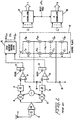
- According to theory, an IQ radio receiver can be constructed according to Figure 1, in which the radio signal S from the antenna 1 is applied directly to two balanced,
quadrature mixers 2a, 2b (mathematically-multiplying devices) where the signal is multiplied respectively by a sine and cosine wave at the carrier frequency of signal S generated by a local oscillator 3. In this manner the I-channel or in-phase signal and the Q-channel or quadrature signal are generated. The multiplication devices yield outputs containing both sum frequency components around 2f and difference frequency components around zero frequency. DC orlow pass filters 4a, 4b eliminate the former and accept the latter. The zero frequency components can then be amplified to any convenient level by low-frequency amplifyingstages - In practice, this so-called zero-IF approach is beset with a variety of practical problems, one of which concerns the imperfection of the balanced mixers as compared to perfect mathematical multipliers. The most troublesome aspect of this imperfection is the generation of a DC offset or standing voltage that can be many orders of magnitude greater than the desired signal. The low frequency amplifiers, which receive the mixer outputs, can be forced into saturation by the large DC offset long before the desired signal has been amplified sufficiently.
- To avoid premature saturation, RF amplifers can be added ahead of the mixers to raise the desired signal voltage level. Unfortunately, a common source of the offset is leakage from the local sinusoidal oscillator back to the antenna, producing coherent interference. As a result, RF amplification is not a satisfactory solution because the desired signal and coherent interference are amplified equally.
- Another proposed solution used in conventional superheterodyne radio receivers is partial amplification of the input signal at the original antenna frequency. The partially amplified signal is then converted to a convenient intermediate frequency IF for further amplification before being applied to the balanced quadrature mixers. In this situation, the locally generated sine and cosine waves are at the IF rather than the antenna frequency, so leakage back to the antenna is of no consequence. However, by adding IF tuning circuitry, the simplicity and reduced size of the zero-IF receiver are lost. An alternative method of overcoming DC offset from the IQ mixers may employ the technique variously called AC coupling, DC blocking, high-pass filtering or differentiation to eliminate the standing or DC offset voltage. The trade-off with this method is the result that the DC and low-frequency components are lost or gravely distorted. This trade-off is unacceptable in digital transmission systems which use QPSK (Quadrature Phase Shift Keying) or MSK (Minimum Shift Keying) modulation techniques. These modulation techniques generate low frequency components that must be preserved.
- U.S. Patent No. 5,241,702 discloses a method of compensating for low frequency offset without losing or distorting the DC and low-frequency components of the desired signal. Initially, the received signal is differentiated to filter out the DC offset. The signal is amplified to a suitable level and then integrated to recapture the original DC and low frequency signal components. The integration essentially restores the filtered components to their original values in the amplified signal using an arbitrary constant of integration of bounded magnitude to generate a restored signal. Using various techniques that exploit predetermined signal patterns or inherent signal properties of the desired signal, the DC offset estimate is then substracted out of the restored signal leaving the amplified, received signal substantially free from distortion. A preferred way of removing such unwanted DC offsets by means of digitizing the time derivatives of the I and Q waveforms will now be described. After digitizing the derivatives, the digital values are re-integrated in an I and a Q accumulator to restore the I,Q values. The re-integration process introduces arbitrary constants of integration into the I and Q values which are now however of comparable magnitude to the wanted signal and can be estimated and removed according to the aforementioned patent. Errors in the digitizing process can lead additionally to the re-integrated I and Q values exhibiting a systematic increase or decrease, and this unwanted slope is now removed at the same time as removing the unwanted arbitrary constants of re-integration by estimating both the constants and the slopes and subtracting these systematic errors from the I and Q waveforms respectively. The I and Q waveforms are then processed by numerical signal processing algorithms to demodulate and decode the information.
- However, problems still remain even for the above identified methods. Rate of change of the DC offset or signal slope still causes problems. Therefore, it is desirable to provide a method for compensating for the rate of change or signal slope so that decoded information modulated on the radio input signal is substantially unimpaired.
- It is on object of the present invention to provide a method for compensating for the rate of change or signal slope so that decoded information modulated on the radio input signal is substantially unimpaired. A radio receiver according to one embodiment of the present invention receives a signal via an antenna and mixes it down to the complex baseband using a local reference oscillator. The complex baseband signal comprises a real part (I waveform) and an imaginary part (Q waveform) that are corrupted by DC offsets arising from mixer imperfections or from reference oscillator leakage radiation being received at the antenna as coherent self-interference.
- According to one embodiment of the present invention, previously estimated errors are fed back to the digitization process to reduce errors in digitizing the derivatives of the I,Q signals. A preferred digitizing technique uses high bit-rate delta modulation with variable stepsize. The variable stepsize is obtained by switching positive and negative current sources of different current values to charge a principal integrator capacitor. Slope errors occur when a positive and negative current source pair do not produce equal current magnitudes. According to one embodiment of the present invention, the unequal current source values are compensated by using correspondingly unequal digital increment/decrement values that are applied to the re-integrating I,Q accumulators, the values being set by a calibration procedure or being updated by feedback calculated from the estimated slope errors.
- According to one embodiment of the present invention, an improved radio receiving apparatus for direct conversion of signals to a baseband for processing is disclosed. The radio receiving apparatus comprises direct conversion means for converting a radio input signal to a complex baseband signal having a real waveform and an imaginary waveform. Slope and offset compensation means estimate offsets and systematic drifts in the real and imaginary waveforms and compensate for the drifts and offsets such that decoding of information modulated on the radio input signal is substantially unimpaired.
- According to another embodiment of the present invention, an improved analog-to-digital conversion apparatus is disclosed. Comparator means compare an input signal voltage with a feedback voltage and generating a high/low indication at a regular repetition rate determined by a clock pulse train. A principal integrator means integrates a controlled current to generate the feedback voltage. Charge pump means produce said controlled current controlled in magnitude by a stepsize controller and in direction or sign in accordance with the high/low indication. Stepsize controller means controls said current magnitude in dependence on historical values of the high/low indications and produces a digital stepsize value indicative of the current magnitude generated by the charge pump for a positive-direction of current flow and a negative direction of current flow respectively. Accumulator means add or subtract the digital stepsize value to produce a series of accumulated digital values representative of the input signal voltage waveform.
- According to one embodiment of the present invention, a method for processing a signal modulated with information symbols to account for an additive offset and slope is disclosed. First, an initial estimate of offset and slope is made and hypotheses of all possible values of a sequence of one or more information symbols are then made. For each of said hypotheses, the associated data symbol sequence is used to make an improved estimate of offset and slope and the improved estimate of offset and slope are stored against each of the hypotheses. For each hypothesis, the improved estimate of offset and slope is used in calculating an expected signal value and a mismatch between a sample of the modulated signal and the expected value is computed. The hypotheses are then sequentially extended by one symbol, the slope and offset estimates are updated and the mismatches are accumulated to form a path metric value for each extended hypothesis, and resolving between said hypotheses based on said path metric values using a Viterbi Sequential Maximum Likelihood Sequence Estimation process to produce a most likely hypothesis of said modulated information symbols substantially unimpaired by said additive slope and offset.
- These and other features and advantages of the invention will be readily apparent to one of ordinary skill in the art from the following written description, used in conjunction with the drawings, in which:
- Figure 1 illustrates a simple block diagram showing a prior art receiver using the zero-IF technique;
- Figure 2 illustrates a prior art homodyne receiver;
- Figure 3 illustrates slope error compensation in an A-to-D convertor according to one embodiment of the present invention; and
- Figure 4 illustrates slope compensation after A-to-D conversion of the I and Q waveforms.
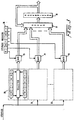
- Figure 2 illustrates a direct conversion receiver 10 according to the principles of U.S. Patent No. 5,241,702, which is incorporated herein by reference in its entirety. An antenna 11 receives a radio signal which is filtered in a filter 12 to remove strong out-of-band interferers. The filtered signal is then amplified in a low-noise amplifier 13 and downconverted in
quadrature mixers local reference oscillator 16 which is tuned nominally to the center of the channel frequency being received. The complex baseband signals frommixers channel filters mixers filters mixers oscillator 16 being received at antenna 11 as coherent self-interference, it does not help to increase the amplification in the amplifier 13 since this will just increase the DC offsets as well as the wanted signal without improving their ratio. - According to the principles of U.S. Patent No. 5,241,702, the DC offset from the
mixers - The I and Q channel signals are thus digitized preferably after differentiation to remove the static DC offset components, and this is accomplished by means of a delta-modulation convertor. The delta modulation convertor for each channel comprises a
principal integrator capacitor Comparators latches control logic unit 25 to provide up/down commands to the charge pumps 26. Thecomparators comparators - To provide the receiver with a high dynamic range, i.e., the ability to handle wanted signal levels ranging from the noise level to perhaps 100dB stronger than the noise level, the delta modulation technique can incorporate variable stepsize or compounding whereby the step
control logic unit 25 can enable charge pumps of different current magnitudes according to the need to cause principal integrator capacitors to follow a large signal swing or a small signal swing. A typical companding principle is to decide to increase the stepsize or charge pump current ifcomparator logic unit 25, while no decision to increase the stepsize causes the stepsize register to be reduced using a decrement. While different increments and decrements giving different companding laws are well known and are not material to the general principal of the present invention, it is important however that companding be applied jointly to both the I and Q channel delta modulators by means of a common stepsize register so as to preserve equality of gain in the two channels. - The value momentarily residing in the stepsize register may be used to determine a corresponding current pulse value from the charge pumps 26 by, for example, constructing a series of charge pumps having current magnitudes in the binary ratios of 1, 1/2, 1/4, 1/8 .... and enabling each according to a corresponding binary bit in the stepsize register. Thus, if the stepsize register contained the value 100000, only the current source having the largest current value of 1 unit would be enabled, while if the register contained 01010000, then a curent value of 1/2 + 1/8 = 0.625 units would be obtained. The sign of the current is determined by the sign of the comparison latched in the
latch 23 for the I channel and thelatch 24 for the Q channel, and causes either a P-type current source connected to the positive supply rail to be enabled to charge the associated capacitor to a higher voltage or an N-type current source connected to the -ve supply rail to be enabled to discharge the capacitor to a lower voltage. The magnitude of the charge or discharge current is however decided by the bit content of the step control register. - The
capacitors Accumulators accumulators - A preferred method of carrying out operations on the output signals from the
accumulators - In this process, it is also possible to use the known training pattern to estimate the constants of integration as well as the echos, and the estimated constants of integration are simply added to the I,Q predictions made using the echo estimates and a data sequence postulate to predict the I,Q value that should be received including said constant offsets. The constant offsets of reintegration are thereby prevented from contributing to the cumulative path metric of the Viterbi equalizer and thus do not cause an error in the determination of the most likely data symbol sequence.
- In the receiver illustrated in Figure 2, the digital output values from I,
Q accumulators capacitors control logic unit 25. It is, however, practically impossible to achieve exact correspondence between the currents generated by charge pumps 26 and the stepsize register values. There are known differences in the physics of P-type and N-type field effect transistors and between NPN and PNP bipolar transistors that make it difficult to obtain a negative current source of exactly the same magnitude as the associated positive current source. Thus, when a positive current source is enabled and a corresponding stepsize register value V is added to an accumulator, followed by a negative current source being enabled and the value V is subtracted from the accumulator, the accumulator value will return to exactly the original value while the corresponding capacitor voltage will not, owing to the small difference between the charge and discharge currents. Thus, after a train of up/down commands, the capacitor voltage and the accumulator voltage will diverge. The negative feedback inherent in the delta modulation process forces the capacitor to follow the input signal, but the accumulator value will diverge by a increasing amount per up/down pair and thus exhibit a slope error which could eventually cause overflow. This problem of divergence between the accumulator values and the true I,Q values is solved by the present invention. - One embodiment of the present invention comprises inclusion of slope error compensation within the delta-modulation AtoD conversion process and more specifically within the digital re-integration process. Figure 3 illustrates one method of compensating slope errors according to the present invention. A number of
selector gates selectors - Each register pair and associated selector corresponds to a particular bit in the stepsize register. In the prior art, a bit in the stepsize register indicated a current magnitude according to its significance, the bits being always in the series 1, 1/2, 1/4, 1/8.... relative to each other. The sign of the current was indicated by the stepsign bit, so the magnitude indicated by a particular stepsize bit was the same regardless of sign. The actual positive and negative current sources cannot be perfectly matched, thus giving rise to the slope error. In the arrangement illustrated in Figure 3, the magnitudes stored in the register pairs are independent for the positive and negative stepsign. Moreover, the values associated with different stepsize register bits are not constrained to bear a power of two relationship to each other. Rather, each register may be programmed with a value representing the actual current of the positive or negative current source that is enabled by a particular bit of the stepsize register. Thus, when a current source or combination of current sources is enabled to increase or decrease the charge on the principal integrator capacitor, the
accumulator 38 will be increased or decreased with an exact corresponding value. This occurs through each bit that is equal to a binary "1" in astepsize register 36 enabling an associatedgate selector adder 37. Thus, the digital values selected to be added in theadder 37 to theaccumulator 38 correspond to the analog current source values that are enabled bystepsize register 36 and the stepsign bit to sum into the principal integrator capacitor. Thus, the accumulator value will follow more accurately the voltage changes on the principal integrator capacitor that in turn follow the wanted signal component. The accuracy is optimized by programming values into register/selector circuits registers - It is also possible to learn the correct contents of
registers logic unit 25 incorporating the inventive arrangement of Figure 3. Denoting the number of times each current source Ii is activated by Ni, then the following equation should hold:
- It may not be necessary to execute the Kalman procedure so often, as the calibration of hardware-related parameters is not expected to change rapidly. It is possible to accumulate a number of the above equations into groups having similar Ni values and then to process the accumulated groups only occasionally, in order to conserve processor power. For example, if all the equations having N1 as the largest coefficient are summed into a group 1, the sum of the N1 coefficients will increasingly come to dominate over the sums of the others. Likewise, if all the equations having N2 as the largest coefficient are summed into a group 2, then the sum of the N2 coefficients will come to dominate. The accumulation of equations into m groups in this way will give a cumulative equation set that tends more to have a diagonal coefficient matrix, such being the most well-conditioned for solution either directly or by the sequential Kalman technique.
- An alternative technique for slope compensation is illustrated in Figure 4. Figure 4 illustrates a pair of I and Q waveforms that are represented by a sequence of complex number samples after the digitization process. Initially, it is assumed the I and Q accumulators were set to zero just before information bearing signal samples were received. Since it could not be known if the received signal plus noise was indeed zero at the reset instant, the error known as the arbitrary constant of re-integration is introduced, which however is now of magnitude no greater than the wanted signal changes. Figure 4 illustrates I,Q waveforms having both this constant offset and a systematic slope. The offsets and slopes are independent for the I and Q waveforms and have to be separately determined. One simple method is to simply fit the best straight line to the digitized value sequence of the form

- In "per-state Kalman", a Viterbi sequential maximum likelihood sequence estimation procedure for decoding data sequences maintains a number of as-yet unresolved data sequence hypotheses. Associated with each hypothesis of the data sequence to date, an estimate of the slope and offsets of the I,Q waveforms can be made with the effect of the hypothesized data sequence removed. For each state, a path metric is computed according to known Viterbi techniques and indicates the likelihood of the associated data sequence hypothesis being correct. The collection of parameters associated with each data sequence hypothesis is known as a "State Memory". The offset and slope stored in a particular state is used to predice the next I,Q value first on the assumption that the next data bit is a 0 and then on the assumption that it is a binary 1. The mismatch between the predicted and actual I,Q values is computed and added to the cumulative path metric to obtain new path metrics. In this way, the number of states is first doubled, but then may be halved by selecting to retain only the best of the pairs of states agreeing in all but their oldest bits. The retained states comprise data sequence hypotheses that have been extended by one data symbol, and the estimates of the slope and offset in each state may now be updated on the assumption that the new symbol that has just been added to each extended data sequence is true. Finally, the state having the lowest path metric is selected to give the decoded data sequence that is most likely to be true, and the associated I,Q slopes and offsets are the best estimates of same with that data sequence having been specifically accounted for. The slope errors may be used then, for example, to correct the AtoD conversion process by the means shown in Figure 3, or by simpler means such as adjusting the relative values of positive and negative current sources by feeding back a control signal. It will be understood by those skilled in the art that the digital information can be modulated onto the radio input signal using a variety of techniques. For example the digital information can be modulated using manchester-code frequency modulation, Gaussian Minimum Shift Keying, DQPSK and Pi/4-DQPSK.
- The improvement to zero-IF receivers described above and comprising correction of both offset and slope compensation of I,Q waveforms is not meant to be limiting but rather exemplary, and a person skilled in the art will be able to suggest other means of implementing slope compensation that nevertheless are considered to fall within the spirit of the invention as set out in the following claims. The scope of the invention is indicated by the appended claims rather than the foregoing description, and all changes which come within the meaning and range of equivalents thereof are intended to be embraced therein.
Claims (6)
- A method for processing a signal modulated with information symbols to account for an additive offset and slope in said signal, comprising:making an initial estimate of offset and slope errors in said modulated information symbols;making hypotheses of possible values of a sequence of one or more information symbols within a predefined period of time;for each of said hypotheses a data symbol sequence associated with said hypotheses can be used to make an improved estimate of offset and slope and storing the improved estimate of offset and slope against each of said hypotheses;for each hypothesis using said improved estimate of offset and slope in calculating an expected signal value and computing a mismatch between a sample of said modulated signal and said expected value;sequentially adding one symbol to said hypothesis, updating said slope and offset estimates and accumulating said mismatches to form a path metric value for each extended hypothesis; andselecting between said hypotheses based on said path metric values using a Viterbi Sequential Maximum Likelihood Sequence Estimation process to produce a most likely hypothesis of modulated information symbols which are unimpaired by said additive slope and offset.
- A method according to claim 1, wherein said digital information is manchester-code frequency modulated on to said radio input signal.
- A method according to claim 1, wherein said digital information is modulated on to said radio input signal using Gaussian Minimum Shift Keying.
- A method according to claim 1, wherein said digital information is modulated on to said radio input signal using DQPSK or Pi/4-DQPSK.
- A method according to claim 1, wherein said information is digital information.
- A method according to claim 5, wherein said digital information represents a digitized voice signal.
Applications Claiming Priority (3)
| Application Number | Priority Date | Filing Date | Title |
|---|---|---|---|
| US401127 | 1995-03-09 | ||
| US08/401,127 US5568520A (en) | 1995-03-09 | 1995-03-09 | Slope drift and offset compensation in zero-IF receivers |
| EP96911247A EP0813768B1 (en) | 1995-03-09 | 1996-03-01 | Slope, drift and offset compensation in zero-if receivers |
Related Parent Applications (2)
| Application Number | Title | Priority Date | Filing Date |
|---|---|---|---|
| EP96911247A Division EP0813768B1 (en) | 1995-03-09 | 1996-03-01 | Slope, drift and offset compensation in zero-if receivers |
| EP96911247.3 Division | 1996-09-19 |
Publications (3)
| Publication Number | Publication Date |
|---|---|
| EP0952665A2 true EP0952665A2 (en) | 1999-10-27 |
| EP0952665A3 EP0952665A3 (en) | 2002-07-10 |
| EP0952665B1 EP0952665B1 (en) | 2005-06-08 |
Family
ID=23586418
Family Applications (2)
| Application Number | Title | Priority Date | Filing Date |
|---|---|---|---|
| EP99115051A Expired - Lifetime EP0952665B1 (en) | 1995-03-09 | 1996-03-01 | Slope, drift and offset compensation in zero-if receivers |
| EP96911247A Expired - Lifetime EP0813768B1 (en) | 1995-03-09 | 1996-03-01 | Slope, drift and offset compensation in zero-if receivers |
Family Applications After (1)
| Application Number | Title | Priority Date | Filing Date |
|---|---|---|---|
| EP96911247A Expired - Lifetime EP0813768B1 (en) | 1995-03-09 | 1996-03-01 | Slope, drift and offset compensation in zero-if receivers |
Country Status (11)
| Country | Link |
|---|---|
| US (3) | US5568520A (en) |
| EP (2) | EP0952665B1 (en) |
| JP (1) | JP3996593B2 (en) |
| KR (1) | KR100366321B1 (en) |
| CN (1) | CN1075283C (en) |
| AU (1) | AU709812B2 (en) |
| BR (1) | BR9607642A (en) |
| CA (1) | CA2213855C (en) |
| DE (2) | DE69634835T2 (en) |
| SG (1) | SG87773A1 (en) |
| WO (1) | WO1996028885A1 (en) |
Families Citing this family (64)
| Publication number | Priority date | Publication date | Assignee | Title |
|---|---|---|---|---|
| US5838735A (en) * | 1996-07-08 | 1998-11-17 | Telefonaktiebolaget Lm Ericsson | Method and apparatus for compensating for a varying d.c. offset in a sampled signal |
| US6006079A (en) * | 1997-06-13 | 1999-12-21 | Motorola, Inc. | Radio having a fast adapting direct conversion receiver |
| DE69831789T2 (en) * | 1997-08-08 | 2006-07-06 | Sony Deutschland Gmbh | CALIBRATION OF AN N-PORT RECEIVER |
| US6205183B1 (en) | 1998-05-29 | 2001-03-20 | Ericsson Inc. | Methods of suppressing reference oscillator harmonic interference and related receivers |
| US7065327B1 (en) | 1998-09-10 | 2006-06-20 | Intel Corporation | Single-chip CMOS direct-conversion transceiver |
| US6246867B1 (en) * | 1998-11-17 | 2001-06-12 | Telefonaktiebolaget Lm Ericsson (Publ) | Method and apparatus for saving current while performing signal strength measurements in a homodyne receiver |
| WO2000039923A1 (en) | 1998-12-24 | 2000-07-06 | Telefonaktiebolaget Lm Ericsson (Publ) | Communication receiver having reduced dynamic range |
| US6567475B1 (en) | 1998-12-29 | 2003-05-20 | Ericsson Inc. | Method and system for the transmission, reception and processing of 4-level and 8-level signaling symbols |
| SE9900289D0 (en) * | 1999-01-27 | 1999-01-27 | Ericsson Telefon Ab L M | DC estimate method for a homodyne receiver |
| US6516185B1 (en) * | 1999-05-24 | 2003-02-04 | Level One Communications, Inc. | Automatic gain control and offset correction |
| US6430391B1 (en) * | 1999-11-29 | 2002-08-06 | Ericsson Inc. | Duplex satellite communication using a single frequency or pair |
| US6625236B1 (en) | 2000-02-08 | 2003-09-23 | Ericsson Inc. | Methods and systems for decoding symbols by combining matched-filtered samples with hard symbol decisions |
| US7088765B1 (en) | 2000-03-15 | 2006-08-08 | Ndsu Research Foundation | Vector calibration system |
| EP1249116B1 (en) * | 2000-06-27 | 2006-12-27 | Koninklijke Philips Electronics N.V. | Detection and correction of phase jumps in a phase sequence |
| GB2366460A (en) * | 2000-08-24 | 2002-03-06 | Nokia Mobile Phones Ltd | DC compensation for a direct conversion radio receiver |
| US6735422B1 (en) | 2000-10-02 | 2004-05-11 | Baldwin Keith R | Calibrated DC compensation system for a wireless communication device configured in a zero intermediate frequency architecture |
| US6560448B1 (en) * | 2000-10-02 | 2003-05-06 | Intersil Americas Inc. | DC compensation system for a wireless communication device configured in a zero intermediate frequency architecture |
| US7068987B2 (en) | 2000-10-02 | 2006-06-27 | Conexant, Inc. | Packet acquisition and channel tracking for a wireless communication device configured in a zero intermediate frequency architecture |
| US20020114417A1 (en) * | 2000-10-10 | 2002-08-22 | Mcdonagh Stephen J. | Model for charge pump phase-locked loop |
| GB2370928B (en) * | 2001-01-09 | 2004-08-25 | Ericsson Telefon Ab L M | Radio receiver |
| US6961368B2 (en) * | 2001-01-26 | 2005-11-01 | Ericsson Inc. | Adaptive antenna optimization network |
| US7778365B2 (en) * | 2001-04-27 | 2010-08-17 | The Directv Group, Inc. | Satellite TWTA on-line non-linearity measurement |
| US7245671B1 (en) * | 2001-04-27 | 2007-07-17 | The Directv Group, Inc. | Preprocessing signal layers in a layered modulation digital signal system to use legacy receivers |
| US7471735B2 (en) | 2001-04-27 | 2008-12-30 | The Directv Group, Inc. | Maximizing power and spectral efficiencies for layered and conventional modulations |
| US7822154B2 (en) * | 2001-04-27 | 2010-10-26 | The Directv Group, Inc. | Signal, interference and noise power measurement |
| US7209524B2 (en) * | 2001-04-27 | 2007-04-24 | The Directv Group, Inc. | Layered modulation for digital signals |
| US8005035B2 (en) * | 2001-04-27 | 2011-08-23 | The Directv Group, Inc. | Online output multiplexer filter measurement |
| US7184473B2 (en) * | 2001-04-27 | 2007-02-27 | The Directv Group, Inc. | Equalizers for layered modulated and other signals |
| US7184489B2 (en) * | 2001-04-27 | 2007-02-27 | The Directv Group, Inc. | Optimization technique for layered modulation |
| US7423987B2 (en) * | 2001-04-27 | 2008-09-09 | The Directv Group, Inc. | Feeder link configurations to support layered modulation for digital signals |
| US7502430B2 (en) * | 2001-04-27 | 2009-03-10 | The Directv Group, Inc. | Coherent averaging for measuring traveling wave tube amplifier nonlinearity |
| US7483505B2 (en) * | 2001-04-27 | 2009-01-27 | The Directv Group, Inc. | Unblind equalizer architecture for digital communication systems |
| US7583728B2 (en) * | 2002-10-25 | 2009-09-01 | The Directv Group, Inc. | Equalizers for layered modulated and other signals |
| US7173981B1 (en) * | 2001-04-27 | 2007-02-06 | The Directv Group, Inc. | Dual layer signal processing in a layered modulation digital signal system |
| US7039382B2 (en) * | 2001-05-15 | 2006-05-02 | Broadcom Corporation | DC offset calibration for a radio transceiver mixer |
| US7231000B2 (en) | 2001-10-22 | 2007-06-12 | Broadcom Corporation | System and method for DC offset compensation and bit synchronization |
| US7038733B2 (en) * | 2002-01-30 | 2006-05-02 | Ericsson Inc. | Television receivers and methods for processing signal sample streams synchronously with line/frame patterns |
| AU2003280499A1 (en) * | 2002-07-01 | 2004-01-19 | The Directv Group, Inc. | Improving hierarchical 8psk performance |
| ES2604453T3 (en) | 2002-07-03 | 2017-03-07 | The Directv Group, Inc. | Method and apparatus for layered modulation |
| US7230480B2 (en) * | 2002-10-25 | 2007-06-12 | The Directv Group, Inc. | Estimating the operating point on a non-linear traveling wave tube amplifier |
| CA2503530C (en) | 2002-10-25 | 2009-12-22 | The Directv Group, Inc. | Lower complexity layered modulation signal processor |
| AU2003282854A1 (en) * | 2002-10-25 | 2004-05-25 | The Directv Group, Inc. | Method and apparatus for tailoring carrier power requirements according to availability in layered modulation systems |
| US7474710B2 (en) * | 2002-10-25 | 2009-01-06 | The Directv Group, Inc. | Amplitude and phase matching for layered modulation reception |
| US7529312B2 (en) * | 2002-10-25 | 2009-05-05 | The Directv Group, Inc. | Layered modulation for terrestrial ATSC applications |
| US7206557B2 (en) * | 2003-01-08 | 2007-04-17 | Lucent Technologies Inc. | Method and apparatus for suppressing local oscillator leakage in a wireless transmitter |
| US7215722B2 (en) * | 2003-06-09 | 2007-05-08 | Ali Corporation | Device for WLAN baseband processing with DC offset reduction |
| US7502429B2 (en) * | 2003-10-10 | 2009-03-10 | The Directv Group, Inc. | Equalization for traveling wave tube amplifier nonlinearity measurements |
| US7251300B2 (en) * | 2003-12-22 | 2007-07-31 | Spreadtrum Communications Corporation | Method and apparatus for frequency tracking based on recovered data |
| DE10361037A1 (en) * | 2003-12-23 | 2005-07-28 | Infineon Technologies Ag | Method and device for demodulating a phase-modulated signal |
| US7526265B2 (en) | 2005-05-24 | 2009-04-28 | Skyworks Solutions, Inc. | Method and system for receiver impairment estimation and correction |
| JP4516501B2 (en) * | 2005-08-25 | 2010-08-04 | 富士通オプティカルコンポーネンツ株式会社 | DQPSK optical receiver circuit |
| EP1952531A1 (en) * | 2005-11-18 | 2008-08-06 | Koninklijke Philips Electronics N.V. | Dc offset estimation |
| WO2008047874A1 (en) | 2006-10-19 | 2008-04-24 | Nec Corporation | Signal generation device, method, and its program in radio transmission system |
| GB0803710D0 (en) * | 2008-02-28 | 2008-04-09 | Nokia Corp | DC compensation |
| US8351874B2 (en) * | 2008-04-08 | 2013-01-08 | Telefonaktiebolaget Lm Ericsson (Publ) | System and method for adaptive antenna impedance matching |
| CN101610090B (en) * | 2008-06-20 | 2012-10-10 | 大唐移动通信设备有限公司 | Zero intermediate frequency transmitter and method for calibrating zero intermediate frequency transmitting signal |
| US8855580B2 (en) * | 2008-06-27 | 2014-10-07 | Telefonaktiebolaget L M Ericsson (Publ) | Methods and apparatus for reducing own-transmitter interference in low-IF and zero-IF receivers |
| US7995973B2 (en) * | 2008-12-19 | 2011-08-09 | Telefonaktiebolaget Lm Ericsson (Publ) | Own transmitter interference tolerant transceiver and receiving methods |
| US8055234B2 (en) * | 2008-06-27 | 2011-11-08 | Telefonaktiebolaget Lm Ericsson (Publ) | Methods and apparatus for suppressing strong-signal interference in low-IF receivers |
| US8120466B2 (en) * | 2008-10-08 | 2012-02-21 | Assa Abloy Ab | Decoding scheme for RFID reader |
| US8090320B2 (en) * | 2008-12-19 | 2012-01-03 | Telefonaktiebolaget Lm Ericsson (Publ) | Strong signal tolerant OFDM receiver and receiving methods |
| CN101478317B (en) * | 2008-12-25 | 2012-02-01 | 苏州全波通信技术有限公司 | IQ amplitude adaptive balance system in direct frequency conversion modulation |
| CN103414486B (en) * | 2013-08-19 | 2015-12-09 | 电子科技大学 | The zero intermediate frequency I/Q mismatch compensation circuit of 60GHz communication system |
| CN109728856B (en) * | 2017-10-27 | 2021-12-31 | 富士通株式会社 | Estimation device and compensation device for IQ imbalance of optical transmitter and electronic equipment |
Citations (4)
| Publication number | Priority date | Publication date | Assignee | Title |
|---|---|---|---|---|
| EP0343273A1 (en) * | 1988-05-27 | 1989-11-29 | Deutsche ITT Industries GmbH | Correction circuit for a pair of digital quadrature signals |
| US5241702A (en) * | 1990-09-06 | 1993-08-31 | Telefonaktiebolaget L M Ericsson | D.c. offset compensation in a radio receiver |
| GB2267629A (en) * | 1992-06-03 | 1993-12-08 | Fujitsu Ltd | Signal error reduction in receiving apparatus |
| EP0594894A1 (en) * | 1992-10-28 | 1994-05-04 | ALCATEL BELL Naamloze Vennootschap | DC offset correction for direct-conversion TDMA receiver |
Family Cites Families (6)
| Publication number | Priority date | Publication date | Assignee | Title |
|---|---|---|---|---|
| US4729110A (en) * | 1984-12-24 | 1988-03-01 | General Electric Company | Correction of offset and gain errors in RF receivers |
| DE3779638T2 (en) * | 1987-09-03 | 1993-01-21 | Philips Nv | RECEIVER WITH PARALLEL SIGNALS. |
| SE462942B (en) * | 1989-01-26 | 1990-09-17 | Ericsson Telefon Ab L M | SETTING AND DEVICE FOR FAST SPEED CONTROL OF A COHERENT RADIO RECEIVER |
| SE465245B (en) * | 1989-12-22 | 1991-08-12 | Ericsson Telefon Ab L M | PROCEDURE TO PERFORM CHANNEL ESTIMATES FOR A FAITHFUL CHANNEL FOR TRANSFER OF SYMBOL SEQUENCES |
| US5303412A (en) * | 1992-03-13 | 1994-04-12 | Massachusetts Institute Of Technology | Composite direct digital synthesizer |
| US5166641A (en) * | 1992-03-17 | 1992-11-24 | National Semiconductor Corporation | Phase-locked loop with automatic phase offset calibration |
-
1995
- 1995-03-09 US US08/401,127 patent/US5568520A/en not_active Expired - Lifetime
-
1996
- 1996-03-01 CA CA002213855A patent/CA2213855C/en not_active Expired - Fee Related
- 1996-03-01 DE DE69634835T patent/DE69634835T2/en not_active Expired - Lifetime
- 1996-03-01 DE DE69608884T patent/DE69608884T2/en not_active Expired - Lifetime
- 1996-03-01 EP EP99115051A patent/EP0952665B1/en not_active Expired - Lifetime
- 1996-03-01 BR BR9607642A patent/BR9607642A/en not_active IP Right Cessation
- 1996-03-01 AU AU54190/96A patent/AU709812B2/en not_active Ceased
- 1996-03-01 CN CN96193645A patent/CN1075283C/en not_active Expired - Fee Related
- 1996-03-01 SG SG9803592A patent/SG87773A1/en unknown
- 1996-03-01 WO PCT/US1996/002983 patent/WO1996028885A1/en active IP Right Grant
- 1996-03-01 EP EP96911247A patent/EP0813768B1/en not_active Expired - Lifetime
- 1996-03-01 KR KR1019970706289A patent/KR100366321B1/en not_active IP Right Cessation
- 1996-07-25 US US08/686,399 patent/US5712637A/en not_active Expired - Lifetime
- 1996-08-13 US US08/699,774 patent/US6473471B2/en not_active Expired - Lifetime
-
2004
- 2004-11-04 JP JP2004320731A patent/JP3996593B2/en not_active Expired - Lifetime
Patent Citations (4)
| Publication number | Priority date | Publication date | Assignee | Title |
|---|---|---|---|---|
| EP0343273A1 (en) * | 1988-05-27 | 1989-11-29 | Deutsche ITT Industries GmbH | Correction circuit for a pair of digital quadrature signals |
| US5241702A (en) * | 1990-09-06 | 1993-08-31 | Telefonaktiebolaget L M Ericsson | D.c. offset compensation in a radio receiver |
| GB2267629A (en) * | 1992-06-03 | 1993-12-08 | Fujitsu Ltd | Signal error reduction in receiving apparatus |
| EP0594894A1 (en) * | 1992-10-28 | 1994-05-04 | ALCATEL BELL Naamloze Vennootschap | DC offset correction for direct-conversion TDMA receiver |
Non-Patent Citations (1)
| Title |
|---|
| LINDQUIST B ET AL: "A NEW APPROACH TO ELIMINATE THE DC OFFSET IN A TDMA DIRECT CONVERSION RECEIVER" PERSONAL COMMUNICATION - FREEDOM THROUGH WIRELESS TECHNOLOGY, SECAUCUS, NJ., MAY 18 - 20, 1993, no. CONF. 43, 18 May 1993 (1993-05-18), pages 754-757, XP000393292 INSTITUTE OF ELECTRICAL AND ELECTRONICS ENGINEERS * |
Also Published As
| Publication number | Publication date |
|---|---|
| US5712637A (en) | 1998-01-27 |
| DE69608884D1 (en) | 2000-07-20 |
| KR19980702881A (en) | 1998-08-05 |
| US6473471B2 (en) | 2002-10-29 |
| EP0952665A3 (en) | 2002-07-10 |
| DE69608884T2 (en) | 2000-11-02 |
| US20020071506A1 (en) | 2002-06-13 |
| CN1075283C (en) | 2001-11-21 |
| CA2213855A1 (en) | 1996-09-19 |
| AU709812B2 (en) | 1999-09-09 |
| KR100366321B1 (en) | 2003-03-15 |
| JP3690810B2 (en) | 2005-08-31 |
| EP0813768B1 (en) | 2000-06-14 |
| JP3996593B2 (en) | 2007-10-24 |
| CA2213855C (en) | 2006-08-15 |
| DE69634835D1 (en) | 2005-07-14 |
| AU5419096A (en) | 1996-10-02 |
| EP0813768A1 (en) | 1997-12-29 |
| JP2005137014A (en) | 2005-05-26 |
| BR9607642A (en) | 1998-05-26 |
| US5568520A (en) | 1996-10-22 |
| SG87773A1 (en) | 2002-04-16 |
| JPH11502080A (en) | 1999-02-16 |
| DE69634835T2 (en) | 2005-11-24 |
| WO1996028885A1 (en) | 1996-09-19 |
| CN1183179A (en) | 1998-05-27 |
| EP0952665B1 (en) | 2005-06-08 |
Similar Documents
| Publication | Publication Date | Title |
|---|---|---|
| US6473471B2 (en) | Slope drift and offset compensation in zero-if receivers | |
| EP0497433B1 (en) | Phase controlled demodulation system for digital communication | |
| CA2050666C (en) | D.c. offset compensation in a radio receiver | |
| CN101005480B (en) | Demodulation circuit and demodulation method | |
| EP1197049A1 (en) | A method and apparatus for performing dc-offset compensation in a radio receiver | |
| US20010017902A1 (en) | Timing error detection circuit, demodulation circuit and methods thereof | |
| JP5304090B2 (en) | Clock recovery circuit and receiver using the same | |
| US5652541A (en) | Data demodulator employing decision feedback for reference parameter recovery and method used therin | |
| US4071829A (en) | Coherent phase detector using a frequency discriminator | |
| JPS58182903A (en) | Digital demodulator | |
| US11539389B2 (en) | Single channel receiver and receiving method | |
| KR100535774B1 (en) | Apparatus for compensation DC offset and I/Q gain and phase imbalance and compensation system using it | |
| CA2522831C (en) | Slope, drift and offset compensation in zero-if receivers | |
| DE102014104524B4 (en) | Receiver capable of detecting frequency deviations and methods therefor | |
| US20050018792A1 (en) | Timing error detection for a digital receiver | |
| JP3690810B6 (en) | Compensation method for slope, drift and offset in non-intermediate frequency receiver | |
| KR100299661B1 (en) | Method and apparatus for evaluating dc offset in digital quadrature demodulator | |
| KR100275703B1 (en) | Phase tracking circuit and phase detecting method | |
| NZ260297A (en) | Compensating for dc offset in rf signal receiver |
Legal Events
| Date | Code | Title | Description |
|---|---|---|---|
| PUAI | Public reference made under article 153(3) epc to a published international application that has entered the european phase |
Free format text: ORIGINAL CODE: 0009012 |
|
| 17P | Request for examination filed |
Effective date: 19990804 |
|
| AC | Divisional application: reference to earlier application |
Ref document number: 813768 Country of ref document: EP |
|
| AK | Designated contracting states |
Kind code of ref document: A2 Designated state(s): AT BE CH DE DK ES FI FR GB GR IE IT LI LU MC NL PT SE |
|
| AX | Request for extension of the european patent |
Free format text: AL;LT;LV;SI |
|
| PUAL | Search report despatched |
Free format text: ORIGINAL CODE: 0009013 |
|
| AK | Designated contracting states |
Kind code of ref document: A3 Designated state(s): AT BE CH DE DK ES FI FR GB GR IE IT LI LU MC NL PT SE |
|
| AX | Request for extension of the european patent |
Free format text: AL;LT;LV;SI |
|
| AKX | Designation fees paid |
Designated state(s): DE FI FR GB IT SE |
|
| RIN1 | Information on inventor provided before grant (corrected) |
Inventor name: DENT, PAUL W. Inventor name: LINDQUIST, BJOERN |
|
| RAP1 | Party data changed (applicant data changed or rights of an application transferred) |
Owner name: ERICSSON INC. |
|
| 17Q | First examination report despatched |
Effective date: 20040602 |
|
| GRAP | Despatch of communication of intention to grant a patent |
Free format text: ORIGINAL CODE: EPIDOSNIGR1 |
|
| GRAS | Grant fee paid |
Free format text: ORIGINAL CODE: EPIDOSNIGR3 |
|
| GRAA | (expected) grant |
Free format text: ORIGINAL CODE: 0009210 |
|
| AC | Divisional application: reference to earlier application |
Ref document number: 0813768 Country of ref document: EP Kind code of ref document: P |
|
| AK | Designated contracting states |
Kind code of ref document: B1 Designated state(s): DE FI FR GB IT SE |
|
| PG25 | Lapsed in a contracting state [announced via postgrant information from national office to epo] |
Ref country code: IT Free format text: LAPSE BECAUSE OF FAILURE TO SUBMIT A TRANSLATION OF THE DESCRIPTION OR TO PAY THE FEE WITHIN THE PRE;WARNING: LAPSES OF ITALIAN PATENTS WITH EFFECTIVE DATE BEFORE 2007 MAY HAVE OCCURRED AT ANY TIME BEFORE 2007. THE CORRECT EFFECTIVE DATE MAY BE DIFFERENT FROM THE ONE RECORDED.SCRIBED TIME-LIMIT Effective date: 20050608 Ref country code: FI Free format text: LAPSE BECAUSE OF FAILURE TO SUBMIT A TRANSLATION OF THE DESCRIPTION OR TO PAY THE FEE WITHIN THE PRESCRIBED TIME-LIMIT Effective date: 20050608 |
|
| REG | Reference to a national code |
Ref country code: GB Ref legal event code: FG4D |
|
| REF | Corresponds to: |
Ref document number: 69634835 Country of ref document: DE Date of ref document: 20050714 Kind code of ref document: P |
|
| PG25 | Lapsed in a contracting state [announced via postgrant information from national office to epo] |
Ref country code: SE Free format text: LAPSE BECAUSE OF FAILURE TO SUBMIT A TRANSLATION OF THE DESCRIPTION OR TO PAY THE FEE WITHIN THE PRESCRIBED TIME-LIMIT Effective date: 20050908 |
|
| PG25 | Lapsed in a contracting state [announced via postgrant information from national office to epo] |
Ref country code: GB Free format text: LAPSE BECAUSE OF NON-PAYMENT OF DUE FEES Effective date: 20060301 |
|
| PLBE | No opposition filed within time limit |
Free format text: ORIGINAL CODE: 0009261 |
|
| STAA | Information on the status of an ep patent application or granted ep patent |
Free format text: STATUS: NO OPPOSITION FILED WITHIN TIME LIMIT |
|
| 26N | No opposition filed |
Effective date: 20060309 |
|
| EN | Fr: translation not filed | ||
| PG25 | Lapsed in a contracting state [announced via postgrant information from national office to epo] |
Ref country code: FR Free format text: LAPSE BECAUSE OF FAILURE TO SUBMIT A TRANSLATION OF THE DESCRIPTION OR TO PAY THE FEE WITHIN THE PRESCRIBED TIME-LIMIT Effective date: 20060804 |
|
| GBPC | Gb: european patent ceased through non-payment of renewal fee |
Effective date: 20060301 |
|
| PG25 | Lapsed in a contracting state [announced via postgrant information from national office to epo] |
Ref country code: FR Free format text: LAPSE BECAUSE OF FAILURE TO SUBMIT A TRANSLATION OF THE DESCRIPTION OR TO PAY THE FEE WITHIN THE PRESCRIBED TIME-LIMIT Effective date: 20050608 |
|
| PGFP | Annual fee paid to national office [announced via postgrant information from national office to epo] |
Ref country code: DE Payment date: 20140327 Year of fee payment: 19 |
|
| REG | Reference to a national code |
Ref country code: DE Ref legal event code: R119 Ref document number: 69634835 Country of ref document: DE |
|
| PG25 | Lapsed in a contracting state [announced via postgrant information from national office to epo] |
Ref country code: DE Free format text: LAPSE BECAUSE OF NON-PAYMENT OF DUE FEES Effective date: 20151001 |