EP0954067A2 - Grounding terminal and mounting structure of the same on a printed circuit board - Google Patents
Grounding terminal and mounting structure of the same on a printed circuit board Download PDFInfo
- Publication number
- EP0954067A2 EP0954067A2 EP99108326A EP99108326A EP0954067A2 EP 0954067 A2 EP0954067 A2 EP 0954067A2 EP 99108326 A EP99108326 A EP 99108326A EP 99108326 A EP99108326 A EP 99108326A EP 0954067 A2 EP0954067 A2 EP 0954067A2
- Authority
- EP
- European Patent Office
- Prior art keywords
- joint
- printed circuit
- circuit board
- grounding terminal
- grounding
- Prior art date
- Legal status (The legal status is an assumption and is not a legal conclusion. Google has not performed a legal analysis and makes no representation as to the accuracy of the status listed.)
- Granted
Links
Images


Classifications
-
- H—ELECTRICITY
- H05—ELECTRIC TECHNIQUES NOT OTHERWISE PROVIDED FOR
- H05K—PRINTED CIRCUITS; CASINGS OR CONSTRUCTIONAL DETAILS OF ELECTRIC APPARATUS; MANUFACTURE OF ASSEMBLAGES OF ELECTRICAL COMPONENTS
- H05K3/00—Apparatus or processes for manufacturing printed circuits
- H05K3/30—Assembling printed circuits with electric components, e.g. with resistor
- H05K3/32—Assembling printed circuits with electric components, e.g. with resistor electrically connecting electric components or wires to printed circuits
- H05K3/34—Assembling printed circuits with electric components, e.g. with resistor electrically connecting electric components or wires to printed circuits by soldering
- H05K3/341—Surface mounted components
-
- H—ELECTRICITY
- H01—ELECTRIC ELEMENTS
- H01R—ELECTRICALLY-CONDUCTIVE CONNECTIONS; STRUCTURAL ASSOCIATIONS OF A PLURALITY OF MUTUALLY-INSULATED ELECTRICAL CONNECTING ELEMENTS; COUPLING DEVICES; CURRENT COLLECTORS
- H01R12/00—Structural associations of a plurality of mutually-insulated electrical connecting elements, specially adapted for printed circuits, e.g. printed circuit boards [PCB], flat or ribbon cables, or like generally planar structures, e.g. terminal strips, terminal blocks; Coupling devices specially adapted for printed circuits, flat or ribbon cables, or like generally planar structures; Terminals specially adapted for contact with, or insertion into, printed circuits, flat or ribbon cables, or like generally planar structures
- H01R12/50—Fixed connections
- H01R12/51—Fixed connections for rigid printed circuits or like structures
- H01R12/55—Fixed connections for rigid printed circuits or like structures characterised by the terminals
- H01R12/57—Fixed connections for rigid printed circuits or like structures characterised by the terminals surface mounting terminals
-
- H—ELECTRICITY
- H05—ELECTRIC TECHNIQUES NOT OTHERWISE PROVIDED FOR
- H05K—PRINTED CIRCUITS; CASINGS OR CONSTRUCTIONAL DETAILS OF ELECTRIC APPARATUS; MANUFACTURE OF ASSEMBLAGES OF ELECTRICAL COMPONENTS
- H05K1/00—Printed circuits
- H05K1/02—Details
- H05K1/0213—Electrical arrangements not otherwise provided for
- H05K1/0215—Grounding of printed circuits by connection to external grounding means
-
- H—ELECTRICITY
- H01—ELECTRIC ELEMENTS
- H01R—ELECTRICALLY-CONDUCTIVE CONNECTIONS; STRUCTURAL ASSOCIATIONS OF A PLURALITY OF MUTUALLY-INSULATED ELECTRICAL CONNECTING ELEMENTS; COUPLING DEVICES; CURRENT COLLECTORS
- H01R13/00—Details of coupling devices of the kinds covered by groups H01R12/70 or H01R24/00 - H01R33/00
- H01R13/02—Contact members
- H01R13/22—Contacts for co-operating by abutting
- H01R13/24—Contacts for co-operating by abutting resilient; resiliently-mounted
-
- H—ELECTRICITY
- H01—ELECTRIC ELEMENTS
- H01R—ELECTRICALLY-CONDUCTIVE CONNECTIONS; STRUCTURAL ASSOCIATIONS OF A PLURALITY OF MUTUALLY-INSULATED ELECTRICAL CONNECTING ELEMENTS; COUPLING DEVICES; CURRENT COLLECTORS
- H01R4/00—Electrically-conductive connections between two or more conductive members in direct contact, i.e. touching one another; Means for effecting or maintaining such contact; Electrically-conductive connections having two or more spaced connecting locations for conductors and using contact members penetrating insulation
- H01R4/58—Electrically-conductive connections between two or more conductive members in direct contact, i.e. touching one another; Means for effecting or maintaining such contact; Electrically-conductive connections having two or more spaced connecting locations for conductors and using contact members penetrating insulation characterised by the form or material of the contacting members
- H01R4/64—Connections between or with conductive parts having primarily a non-electric function, e.g. frame, casing, rail
-
- H—ELECTRICITY
- H01—ELECTRIC ELEMENTS
- H01R—ELECTRICALLY-CONDUCTIVE CONNECTIONS; STRUCTURAL ASSOCIATIONS OF A PLURALITY OF MUTUALLY-INSULATED ELECTRICAL CONNECTING ELEMENTS; COUPLING DEVICES; CURRENT COLLECTORS
- H01R43/00—Apparatus or processes specially adapted for manufacturing, assembling, maintaining, or repairing of line connectors or current collectors or for joining electric conductors
- H01R43/02—Apparatus or processes specially adapted for manufacturing, assembling, maintaining, or repairing of line connectors or current collectors or for joining electric conductors for soldered or welded connections
- H01R43/0256—Apparatus or processes specially adapted for manufacturing, assembling, maintaining, or repairing of line connectors or current collectors or for joining electric conductors for soldered or welded connections for soldering or welding connectors to a printed circuit board
-
- H—ELECTRICITY
- H05—ELECTRIC TECHNIQUES NOT OTHERWISE PROVIDED FOR
- H05K—PRINTED CIRCUITS; CASINGS OR CONSTRUCTIONAL DETAILS OF ELECTRIC APPARATUS; MANUFACTURE OF ASSEMBLAGES OF ELECTRICAL COMPONENTS
- H05K2201/00—Indexing scheme relating to printed circuits covered by H05K1/00
- H05K2201/09—Shape and layout
- H05K2201/09209—Shape and layout details of conductors
- H05K2201/09654—Shape and layout details of conductors covering at least two types of conductors provided for in H05K2201/09218 - H05K2201/095
- H05K2201/09663—Divided layout, i.e. conductors divided in two or more parts
-
- H—ELECTRICITY
- H05—ELECTRIC TECHNIQUES NOT OTHERWISE PROVIDED FOR
- H05K—PRINTED CIRCUITS; CASINGS OR CONSTRUCTIONAL DETAILS OF ELECTRIC APPARATUS; MANUFACTURE OF ASSEMBLAGES OF ELECTRICAL COMPONENTS
- H05K2201/00—Indexing scheme relating to printed circuits covered by H05K1/00
- H05K2201/10—Details of components or other objects attached to or integrated in a printed circuit board
- H05K2201/10227—Other objects, e.g. metallic pieces
- H05K2201/1031—Surface mounted metallic connector elements
-
- Y—GENERAL TAGGING OF NEW TECHNOLOGICAL DEVELOPMENTS; GENERAL TAGGING OF CROSS-SECTIONAL TECHNOLOGIES SPANNING OVER SEVERAL SECTIONS OF THE IPC; TECHNICAL SUBJECTS COVERED BY FORMER USPC CROSS-REFERENCE ART COLLECTIONS [XRACs] AND DIGESTS
- Y02—TECHNOLOGIES OR APPLICATIONS FOR MITIGATION OR ADAPTATION AGAINST CLIMATE CHANGE
- Y02P—CLIMATE CHANGE MITIGATION TECHNOLOGIES IN THE PRODUCTION OR PROCESSING OF GOODS
- Y02P70/00—Climate change mitigation technologies in the production process for final industrial or consumer products
- Y02P70/50—Manufacturing or production processes characterised by the final manufactured product
-
- Y—GENERAL TAGGING OF NEW TECHNOLOGICAL DEVELOPMENTS; GENERAL TAGGING OF CROSS-SECTIONAL TECHNOLOGIES SPANNING OVER SEVERAL SECTIONS OF THE IPC; TECHNICAL SUBJECTS COVERED BY FORMER USPC CROSS-REFERENCE ART COLLECTIONS [XRACs] AND DIGESTS
- Y10—TECHNICAL SUBJECTS COVERED BY FORMER USPC
- Y10T—TECHNICAL SUBJECTS COVERED BY FORMER US CLASSIFICATION
- Y10T29/00—Metal working
- Y10T29/49—Method of mechanical manufacture
- Y10T29/49002—Electrical device making
- Y10T29/49117—Conductor or circuit manufacturing
- Y10T29/49124—On flat or curved insulated base, e.g., printed circuit, etc.
- Y10T29/49147—Assembling terminal to base
- Y10T29/49149—Assembling terminal to base by metal fusion bonding
Definitions
- the invention relates to a mounting structure of a grounding terminal on a printed circuit board, wherein the printed circuit board is grounded to a grounding conductor by the grounding terminal, which is mounted on the surface of the printed circuit board by reflow soldering, contacting with and being pressed against the grounding conductor.
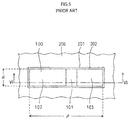
- FIG. 5 is a plan view of such a conventional grounding structure and FIG. 6 is a longitudinal sectional view along line VI-VI of FIG. 5.
- the grounding terminal 100 is soldered to the conductive pattern 201 on the printed circuit board 200 with solder 202. Then, the grounding terminal 100 is pressed against the grounding conductor, thereby grounding the printed circuit board 200.
- the grounding conductor 300 is not shown in FIG. 5.
- the grounding terminal 100 is formed by bending a striplike thin sheet metal member with a width of ⁇ , for example, 0.8mm, and has a joint part 101 with a longitudinal length of ⁇ ,for example, 3.5mm.
- One surface of the joint part 101 is a joint surface 101a which is soldered to the conductive pattern 201 on the printed circuit board 200.
- the grounding terminal has a contact part 102 which adjoins the joint part 101 and is bent in the upper direction. An outer surface 102a of the contact part 102 is pressed against the grounding conductor 300.
- the contact part 102 is elastically deformed around the bending area ⁇ , and is pressed against the grounding conductor 300 by restoring force caused by the elastic deformation, thereby electrically connecting the printed circuit board 200 and the grounding conductor 300 properly.
- Reflow soldering comprises the steps of previously applying a suitable amount of solder to the point to be jointed, fixing the grounding terminal to the point temporarily, and melting the solder by using an external heat source, and all these steps are performed automatically.
- An advantage of reflow soldering is that by allowing a suitable amount of solder to be applied, it prevents solder from being placed at inappropriate points of the printed circuit board, and thus prevents improper soldering such as a defective bridge.
- there is another advantage that in the case where a relatively small mounting member as aforementioned is to be mounted, self-alignment effect can be expected. That is, even if the temporarily fixed member deviates a little from the conductive pattern of the printed circuit board, the member is moved to the right position by surface tension of the melted solder.
- an object of the invention is to provide a mounting structure of a ground terminal on a printed circuit board formed by soldering, wherein by solving the problems caused by reflow soldering of the grounding terminal to the printed circuit board, the printed circuit board is properly grounded to a grounding conductor.
- Another object of the invention is to provide a grounding terminal used for the above mounting structure.
- a grounding terminal mounted on a printed circuit board which is able to have contact with a grounding conductor
- the grounding terminal comprising: a joint part having a plurality of joint surfaces which are to be soldered to a conductive pattern on the printed circuit board; a contact part extending from the joint part through a bending area bent in the opposite direction of the joint surfaces, and arranged to be able to have contact with the grounding conductor, which is elastically deformed upon being pressed by the grounding conductor; and at least one of the contact surfaces of the joint part having a smaller surface area than those of the other contact surfaces.
- a mounting structure in which a grounding terminal able to have contact with a grounding conductor is mounted on a printed circuit board, the grounding terminal comprising: a joint part having a plurality of joint surfaces which are to be soldered to a conductive pattern on the printed circuit board; a contact part extending from the joint part through a bending area bent in the opposite direction of the joint surfaces, and arranged to be able to have contact with the grounding conductor, which is elastically deformed upon being pressed by the grounding conductor; at least one of the contact surfaces of the joint part having a smaller surface area than those of the other contact surfaces; and the grounding terminal being mounted on the printed circuit board by reflow soldering, using an amount of solder corresponding to the surface area of each joint surface.
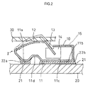
- the grounding structure in the embodiment is formed by soldering a grounding terminal 10 to a printed circuit board 20.
- the grounding terminal 10 soldered to the printed circuit hoard 20 is pressed against a grounding conductor 30, thereby ground the printed circuit board 20 to the grounding conductor 30.
- the grounding conductor 30 is not shown in FIG. 1.
- the grounding conductor 30 may be a chassis or a metal shielding case which covers the printed circuit board 20.
- the grounding terminal 10 in the embodiment is formed by bending a strip-like thin sheet metal member.
- the longitudinal center part of the metal member is a joint part 11, within which the metal member is bent such that the longitudinal section of the metal member forms a trapezoid, in other words, a groove 11d is formed on one side of the joint part 11.
- Two surfaces oppositely positioned across the groove 11d are joint surfaces 11a and 11b.
- the groove 11d is formed at a predetermined distance away from the longitudinal center of the joint part 11, and thus one joint surface 11a is smaller than the other joint surface 11b.
- the metal member is bent in the upper direction at both ends of the joint part 11. At one end, the metal member is bent approximately perpendicularly to the joint part 11, and the bent part is further bent approximately perpendicularly so as to form a U-shaped longitudinal section with the joint part 11. Rectangular plate-like parts 14, which are bent perpendicularly in the direction of the joint part 11, are formed on both sides of the edge of the metal member. Also, projection parts 15 projecting from both sides of the metal member are formed at a predetermined distance away from the edge. The projection parts 15 are made by being separated from the neighboring member of the same shape when the strip-like thin sheet metal member is stamped out from a sheet metal.
- the other end of the metal member is bent at the end of the joint part 11 so as to form a V-shaped longitudinal section.
- the peak of the V-shaped part has a gently curved longitudinal section instead of an acute one.
- a part which also has a gently curved longitudinal section from the peak of the V-shape part toward the edge of the metal member forms, together with the V-shaped part, a contact part 12.
- the part from the end of the contact part 12 to the edge having a straight longitudinal section is bent in the direction of the joint part 11, and forms a restriction part 13.
- the contact part 12 contacts with and is pressed against the grounding conductor 30, thus being elastically deformed around the peak of the above mentioned V-shaped part.
- FIG.2 shows the state that the contact part 12 is elastically deformed by being pressed against the grounding conductor 30.
- Two-dot chain line of FIG. 2 shows the state that the contact part 12 is not pressed against the grounding conductor 30.
- the main function of the plate-like parts 14 is to restrict the movement of the contact part 12 such that the elastic deformation of the contact part 12 is performed without fluctuation.
- the restoring force caused by the elastic deformation makes the contact part 12 securely pressed against the grounding conductor 30, thereby properly grounding the printed circuit board 20 to the grounding conductor 30.
- the mounting structure of the invention is formed by soldering, specifically by reflow soldering, the grounding terminal 10 having the joint part 11, the contact part 12, and the restriction part 13 as above mentioned to the printed circuit board 20.
- a conductive pattern 21 which corresponds to the joint surfaces 11a and 11b configured within the joint part 11 of the grounding terminal 10.
- creamed solder 22a and 22b are applied on the conductive pattern 21 using a known metal mask.
- the grounding terminal 10 is temporarily fixed to a prescribed position on the printed circuit board 20 by taking advantage of adhesion of the creamed solder applied on the conductive pattern 21 of the printed circuit board 20.
- the printed circuit board 20, on which the grounding terminal 10 is temporarily fixed is heated in a reflow furnace to allow the aforementioned creamed solder 22 to be melted, and the soldering steps end.
- the above reflow soldering is automatically performed, by means of total heating such as infrared heating, latent heating of vaporization, hot air circulation heating, and hot plate heating, and local heating using a heating tool, a light beam, a laser beam, and an air heater. Since reflow soldering is known, a detailed explanation of it is omitted.
- grounding structure according to the embodiment of the invention has particular advantages in the process of reflow soldering as explained below. To make the explanation easy to understand, problems in a conventional grounding structure are firstly clarified.
- Another advantage is as follows: in the case where two joint surfaces 11a and 11b having different surface areas are formed within the joint part 11 of the grounding terminal 10, when the printed circuit board 20 with the grounding terminal 10 at the prescribed position thereon is heated in a reflow furnace, the solder 22a applied on the relatively small joint surface 11a is melted earlier than the solder 22b applied on the relatively large joint surface 11b. This may result in what is called tombstone phenomenon (Manhattan phenomenon), which means, in this case, the grounding terminal 10 is made to erect because of the surface tension of the melted solder.
- the creamed solder 22a and 22b which is a paste mixture of powdered solder and a vehicle, is employed.
- a further advantage is as follows: in the mounting structure of the embodiment, the bending area ⁇ is formed at a predetermined distance away from the relatively small joint surface 11a of the joint part 11. As a result, since the creamed solder 22a applied on the smaller joint surface 11a is not sucked up, by wicking phenomenon, to the bending area ⁇ of the contact part 12, the solder 22a does not adhere around the bending area ⁇ . This prevents the elastic deformation performance of the contact part 12 from declining because of the solder adhering around the bending area ⁇ . Thus, the aforementioned problem (B) is solved and the contact part 12 is appropriately pressed against the grounding conductor 30.
- the mounting structure of the embodiment provides another advantage as follows: a restriction part 13 adjacent to the contact part 12 of the grounding terminal 10 is formed so that the stress caused to the contact part 12 by the elastic deformation thereof will not exceed the elastic limit.
- the restriction part 13 restricts the elastic deformation by contacting and pressing its edge to a surface 11c on the reverse side of the joint surface 11b of the joint part 11.
- the predetermined extent means the extent of elastic deformation which does not allow the stress caused to the contact part 12 to exceed the elastic limit. This prevents a permanent deformation of the contact part 12 even though a heavy load is applied thereto.
- the restriction part 13 is formed adjacent to the contact part 12 of the grounding terminal 10 in FIG.
- a restriction part on the reverse side of the joint surfaces 11a and 11b of the joint part 11 as shown in FIG. 3 and 4 such that the restriction part is pressed against the contact part 12.
- a member 16 is formed as part of the metal member such that the member 16 extends from a side end of the top surface of the above mentioned trapezoid part and bent in the upper direction, allowing the top edge of the member 16 to function as a restriction part.
- the trapezoid part of FIG. 2 is redesigned to have a significant elevation, and the trapezoid part 17 functions as a restriction part.
- the mounting structure of the embodiment have solved the problems in soldering the grounding terminal 10 to the printed circuit board 20 by reflow soldering, ensuring that the printed circuit board 20 is properly grounded to the grounding conductor 30.
- two joint surfaces 11a and 11b having different surface areas, respectively, are formed within the joint part 11 of the grounding terminal 10.
- a grounding terminal having a joint part, within which three or more joint surfaces are formed is soldered to a printed circuit board, only one of the joint surfaces needs to be smaller than the others.
- the creamed solder 22a and 22b is applied to both of the two joint surfaces 11a and 11b formed within the joint part 11 of the grounding terminal 10.
- the solder applied on the larger joint surface 11b needs to be creamed solder 22b.
- the adhesion on the larger joint surface 11b is necessary to resist against the surface tension of the solder which is melted first on the smaller joint surface 11a.
Abstract
Description
- The invention relates to a mounting structure of a grounding terminal on a printed circuit board, wherein the printed circuit board is grounded to a grounding conductor by the grounding terminal, which is mounted on the surface of the printed circuit board by reflow soldering, contacting with and being pressed against the grounding conductor.
- Conventionally, a mounting structure of a grounding terminal on a printed circuit board for grounding the printed circuit board, in which a grounding terminal is mounted on the surface of the printed circuit board and pressed against a grounding conductor, is known. FIG. 5 is a plan view of such a conventional grounding structure and FIG. 6 is a longitudinal sectional view along line VI-VI of FIG. 5. As shown in FIG. 6, the
grounding terminal 100 is soldered to theconductive pattern 201 on the printedcircuit board 200 withsolder 202. Then, thegrounding terminal 100 is pressed against the grounding conductor, thereby grounding the printedcircuit board 200. To illustrate the structure simply, thegrounding conductor 300 is not shown in FIG. 5. - The
grounding terminal 100 is formed by bending a striplike thin sheet metal member with a width of α, for example, 0.8mm, and has ajoint part 101 with a longitudinal length of β ,for example, 3.5mm. One surface of thejoint part 101 is ajoint surface 101a which is soldered to theconductive pattern 201 on the printedcircuit board 200. Also, the grounding terminal has acontact part 102 which adjoins thejoint part 101 and is bent in the upper direction. An outer surface 102a of thecontact part 102 is pressed against thegrounding conductor 300. As the result of load by the grounding conductor, thecontact part 102 is elastically deformed around the bending area γ, and is pressed against thegrounding conductor 300 by restoring force caused by the elastic deformation, thereby electrically connecting the printedcircuit board 200 and thegrounding conductor 300 properly. - When the aforementioned grounding terminal is soldered to the printed circuit board, reflow soldering is usually employed. Reflow soldering comprises the steps of previously applying a suitable amount of solder to the point to be jointed, fixing the grounding terminal to the point temporarily, and melting the solder by using an external heat source, and all these steps are performed automatically. An advantage of reflow soldering is that by allowing a suitable amount of solder to be applied, it prevents solder from being placed at inappropriate points of the printed circuit board, and thus prevents improper soldering such as a defective bridge. Also, there is another advantage that in the case where a relatively small mounting member as aforementioned is to be mounted, self-alignment effect can be expected. That is, even if the temporarily fixed member deviates a little from the conductive pattern of the printed circuit board, the member is moved to the right position by surface tension of the melted solder.
- However, there are the following problems in reflow soldering of the above conventional grounding terminal:
- (1) The
grounding terminal 100 is moved to the right position by self-alignment effect by surface tension of the melted solder, and then is finally positioned by hardening of the melted solder. During the hardening process of the solder, thegrounding terminal 100 sometimes deviates from the right position on the printedcircuit board 200 because of, for example, vibration. This results from the fact that since the amount of the solder is large, the thermal capacity of the solder is large, and thus it takes time for the solder to harden. If thegrounding terminal 100 deviates from the right position, thecontact part 102 may not be pressed against thegrounding conductor 300 in an appropriate state. Furthermore, the requirements of highly precise mounting performance for allowing high density mounting are not satisfied. - (2) When the temperature of the
grounding terminal 100 reaches the melting point of the solder earlier than that of theconductive pattern 201 of the printedcircuit board 200, what is called wicking phenomenon occurs, by which thesolder 202 is sucked up along the bending area γ forming the center of elastic deformation of thecontact part 102 shown in FIG. 6. In this case, since thesolder 202 adheres around the bending area γ , the elastic deformation performance of thecontact part 102 is lowered, and thus it is sometimes impossible to attain elastic deformation enough for thecontact part 102 to be pressed against thegrounding conductor 300 and conduct electricity to thegrounding conductor 300. -
- Wherefore, an object of the invention is to provide a mounting structure of a ground terminal on a printed circuit board formed by soldering, wherein by solving the problems caused by reflow soldering of the grounding terminal to the printed circuit board, the printed circuit board is properly grounded to a grounding conductor.
- Another object of the invention is to provide a grounding terminal used for the above mounting structure.
- In order to achieve the above objects, there is provided a grounding terminal mounted on a printed circuit board which is able to have contact with a grounding conductor, the grounding terminal comprising: a joint part having a plurality of joint surfaces which are to be soldered to a conductive pattern on the printed circuit board; a contact part extending from the joint part through a bending area bent in the opposite direction of the joint surfaces, and arranged to be able to have contact with the grounding conductor, which is elastically deformed upon being pressed by the grounding conductor; and at least one of the contact surfaces of the joint part having a smaller surface area than those of the other contact surfaces.
- Also, there is provided a mounting structure in which a grounding terminal able to have contact with a grounding conductor is mounted on a printed circuit board, the grounding terminal comprising: a joint part having a plurality of joint surfaces which are to be soldered to a conductive pattern on the printed circuit board; a contact part extending from the joint part through a bending area bent in the opposite direction of the joint surfaces, and arranged to be able to have contact with the grounding conductor, which is elastically deformed upon being pressed by the grounding conductor; at least one of the contact surfaces of the joint part having a smaller surface area than those of the other contact surfaces; and the grounding terminal being mounted on the printed circuit board by reflow soldering, using an amount of solder corresponding to the surface area of each joint surface.
- The invention will now be described, by way of example, with reference to the accompanying drawings, in which:
- FIG. 1 is a plan view showing the mounting structure of a grounding terminal according to the embodiment of the invention;
- FIG. 2 is a longitudinal sectional view along line II-II of FIG. 1;
- FIGS. 3 and 4 show modifications of the restriction part, respectively, in the invention;
- FIG. 5 is a plan view showing a conventional mounting structure of a grounding terminal on a printed circuit board; and
- FIG. 6 is a longitudinal sectional view along line VI-VI of FIG. 5.
-
- As shown in FIG. 2, the grounding structure in the embodiment is formed by soldering a
grounding terminal 10 to a printedcircuit board 20. Thegrounding terminal 10 soldered to the printedcircuit hoard 20 is pressed against agrounding conductor 30, thereby ground the printedcircuit board 20 to thegrounding conductor 30. To illustrate the structure simply, thegrounding conductor 30 is not shown in FIG. 1. Thegrounding conductor 30 may be a chassis or a metal shielding case which covers the printedcircuit board 20. - The
grounding terminal 10 in the embodiment is formed by bending a strip-like thin sheet metal member. The longitudinal center part of the metal member is ajoint part 11, within which the metal member is bent such that the longitudinal section of the metal member forms a trapezoid, in other words, agroove 11d is formed on one side of thejoint part 11. Two surfaces oppositely positioned across thegroove 11d arejoint surfaces groove 11d is formed at a predetermined distance away from the longitudinal center of thejoint part 11, and thus onejoint surface 11a is smaller than theother joint surface 11b. - The metal member is bent in the upper direction at both ends of the
joint part 11. At one end, the metal member is bent approximately perpendicularly to thejoint part 11, and the bent part is further bent approximately perpendicularly so as to form a U-shaped longitudinal section with thejoint part 11. Rectangular plate-like parts 14, which are bent perpendicularly in the direction of thejoint part 11, are formed on both sides of the edge of the metal member. Also,projection parts 15 projecting from both sides of the metal member are formed at a predetermined distance away from the edge. Theprojection parts 15 are made by being separated from the neighboring member of the same shape when the strip-like thin sheet metal member is stamped out from a sheet metal. - The other end of the metal member is bent at the end of the
joint part 11 so as to form a V-shaped longitudinal section. The peak of the V-shaped part has a gently curved longitudinal section instead of an acute one. A part which also has a gently curved longitudinal section from the peak of the V-shape part toward the edge of the metal member forms, together with the V-shaped part, acontact part 12. The part from the end of thecontact part 12 to the edge having a straight longitudinal section is bent in the direction of thejoint part 11, and forms arestriction part 13. - Once the
grounding terminal 10 is soldered and fixed on the printed circuit board, which is then placed in a metal shielding case and the like, thecontact part 12 contacts with and is pressed against thegrounding conductor 30, thus being elastically deformed around the peak of the above mentioned V-shaped part. - FIG.2 shows the state that the
contact part 12 is elastically deformed by being pressed against thegrounding conductor 30. Two-dot chain line of FIG. 2 shows the state that thecontact part 12 is not pressed against thegrounding conductor 30. The main function of the plate-like parts 14 is to restrict the movement of thecontact part 12 such that the elastic deformation of thecontact part 12 is performed without fluctuation. The restoring force caused by the elastic deformation makes thecontact part 12 securely pressed against thegrounding conductor 30, thereby properly grounding the printedcircuit board 20 to thegrounding conductor 30. - The mounting structure of the invention is formed by soldering, specifically by reflow soldering, the
grounding terminal 10 having thejoint part 11, thecontact part 12, and therestriction part 13 as above mentioned to the printedcircuit board 20. - Specific steps of soldering are explained hereafter.
- On the printed
circuit board 20 is formed aconductive pattern 21, which corresponds to thejoint surfaces joint part 11 of thegrounding terminal 10. Before soldering, creamedsolder 22a and 22b are applied on theconductive pattern 21 using a known metal mask. The groundingterminal 10 is temporarily fixed to a prescribed position on the printedcircuit board 20 by taking advantage of adhesion of the creamed solder applied on theconductive pattern 21 of the printedcircuit board 20. Then the printedcircuit board 20, on which thegrounding terminal 10 is temporarily fixed, is heated in a reflow furnace to allow the aforementioned creamedsolder 22 to be melted, and the soldering steps end. The above reflow soldering is automatically performed, by means of total heating such as infrared heating, latent heating of vaporization, hot air circulation heating, and hot plate heating, and local heating using a heating tool, a light beam, a laser beam, and an air heater. Since reflow soldering is known, a detailed explanation of it is omitted. - The aforementioned grounding structure according to the embodiment of the invention has particular advantages in the process of reflow soldering as explained below. To make the explanation easy to understand, problems in a conventional grounding structure are firstly clarified.
- In a conventional grounding structure shown in FIG. 6, there are the following problems in soldering the grounding
terminal 10 to the printedcircuit board 200 by reflow soldering. - (A) The
grounding terminal 100 is moved to the right position by self-alignment effect caused by the melted solder, and then is fixed at the position by hardening of the melted solder. In this case thegrounding terminal 100 may deviate, during the hardening process, from the right position on the printedcircuit board 200 because of vibration and the like. In the case where the grounding terminal deviates from the right position, thecontact part 102 cannot be appropriately pressed against thegrounding conductor 300, and also the requirements of highly precise mounting performance to allow high density mounting cannot be satisfied. - (B) When the temperature of the
grounding terminal 100 reaches the melting point of the solder earlier than theconductive pattern 201 of the printedcircuit board 200, what is called wicking phenomenon occurs. Wicking phenomenon, here, means a phenomenon that thesolder 202 is sucked up along the bending area γ forming the center of elastic deformation of thecontact part 102 shown in FIG. 6. In this case, since thesolder 202 adheres and hardens around the bending area γ, the elastic deformation performance of thecontact part 102 is lowered, and thus it is sometimes impossible to attain elastic deformation enough for thecontact part 102 to be pressed against thegrounding conductor 300 and conduct electricity to thegrounding conductor 300. -
- In contrast, in the grounding structure according to the embodiment of the invention, two
joint surfaces joint part 11 of the groundingterminal 10. As a result, the creamed solder 22a applied on the relatively smalljoint surface 11a hardens earlier than the creamedsolder 22b applied on the relatively largejoint surface 11b, when the printedcircuit board 20 is cooled after thegrounding terminal 10 is moved to the right position on the printedcircuit board 20 by self-alignment effect caused by the surface tension of the melted creamedsolder 22a and 22b. Accordingly, once the creamed solder 22a applied on the smallerjoint surface 11a hardens, the groundingterminal 10 does not deviate from the right position on the printedcircuit board 20 because of vibration and the like. This reduces the possibility of the groundingterminal 10 deviating from the right position on the printedcircuit board 20 while cooling the printedcircuit board 20, and thus has solved the problems mentioned in (A). Namely, the possibility of thecontact part 12 not being appropriately pressed against the groundingconductor 30 is reduced, and also the requirements of highly precise mounting performance to allow high density mounting are satisfied. - Another advantage is as follows: in the case where two
joint surfaces joint part 11 of the groundingterminal 10, when the printedcircuit board 20 with the groundingterminal 10 at the prescribed position thereon is heated in a reflow furnace, the solder 22a applied on the relatively smalljoint surface 11a is melted earlier than thesolder 22b applied on the relatively largejoint surface 11b. This may result in what is called tombstone phenomenon (Manhattan phenomenon), which means, in this case, the groundingterminal 10 is made to erect because of the surface tension of the melted solder. However, in the embodiment of the invention, the creamedsolder 22a and 22b, which is a paste mixture of powdered solder and a vehicle, is employed. As a result, there is a strong possibility that the adhesion of the creamed solder offsets the force to detach thejoint surface 11b from theconductive pattern 21 on the printedcircuit board 20 caused by the surface tension of the previously melted solder. Moreover, in the embodiment of the invention, since the size of the joint surfaces of 11a and 11b is different, the adhesion of the creamedsolder 22b on the largerjoint surface 11b is probably stronger than the force to detach thejoint surface 11b caused by the surface tension of the melted creamed solder 22a on the smallerjoint surface 11a. Thus tombstone phenomenon is prevented effectively. - A further advantage is as follows: in the mounting structure of the embodiment, the bending area γ is formed at a predetermined distance away from the relatively small
joint surface 11a of thejoint part 11. As a result, since the creamed solder 22a applied on the smallerjoint surface 11a is not sucked up, by wicking phenomenon, to the bending area γ of thecontact part 12, the solder 22a does not adhere around the bending area γ. This prevents the elastic deformation performance of thecontact part 12 from declining because of the solder adhering around the bending area γ. Thus, the aforementioned problem (B) is solved and thecontact part 12 is appropriately pressed against the groundingconductor 30. - The mounting structure of the embodiment provides another advantage as follows: a
restriction part 13 adjacent to thecontact part 12 of the groundingterminal 10 is formed so that the stress caused to thecontact part 12 by the elastic deformation thereof will not exceed the elastic limit. When thecontact part 12 is elastically deformed to a predetermined extent, therestriction part 13 restricts the elastic deformation by contacting and pressing its edge to asurface 11c on the reverse side of thejoint surface 11b of thejoint part 11. The predetermined extent means the extent of elastic deformation which does not allow the stress caused to thecontact part 12 to exceed the elastic limit. This prevents a permanent deformation of thecontact part 12 even though a heavy load is applied thereto. Although therestriction part 13 is formed adjacent to thecontact part 12 of the groundingterminal 10 in FIG. 2, it may be possible to form a restriction part on the reverse side of thejoint surfaces joint part 11 as shown in FIG. 3 and 4 such that the restriction part is pressed against thecontact part 12. In a modification shown in FIG. 3, amember 16 is formed as part of the metal member such that themember 16 extends from a side end of the top surface of the above mentioned trapezoid part and bent in the upper direction, allowing the top edge of themember 16 to function as a restriction part. In a modification shown in FIG. 4, the trapezoid part of FIG. 2 is redesigned to have a significant elevation, and thetrapezoid part 17 functions as a restriction part. - As described above, the mounting structure of the embodiment have solved the problems in soldering the grounding
terminal 10 to the printedcircuit board 20 by reflow soldering, ensuring that the printedcircuit board 20 is properly grounded to thegrounding conductor 30. - The invention is not restricted to the embodiment and may be embodied in various forms without departing from the spirit and the scope of the invention.
- For example, in the mounting structure of the embodiment, two
joint surfaces joint part 11 of the groundingterminal 10. However, when a grounding terminal having a joint part, within which three or more joint surfaces are formed, is soldered to a printed circuit board, only one of the joint surfaces needs to be smaller than the others. - Also, in the mounting structure of the embodiment, the creamed
solder 22a and 22b is applied to both of the twojoint surfaces joint part 11 of the groundingterminal 10. However, in order to prevent tombstone phenomenon, only the solder applied on the largerjoint surface 11b needs to be creamedsolder 22b. In other words, to prevent tombstone phenomenon, the adhesion on the largerjoint surface 11b is necessary to resist against the surface tension of the solder which is melted first on the smallerjoint surface 11a.
Claims (11)
- A grounding terminal arranged and mounted on a printed circuit board in order to contact with a grounding conductor comprising:a joint part having a plurality of joint surfaces which are to be soldered to a conductive pattern on said printed circuit board;a contact part extending from said joint part through a bending area bent in the opposite direction of said joint surfaces, and being able to contact with said grounding conductor, which is elastically deformed upon being pressed by said grounding conductor; andat least one of said joint surfaces of said joint part having a smaller surface area than those of the other joint surfaces.
- A grounding terminal as set forth in claim 1, wherein said bending area is formed at a predetermined distance away from said joint surfaces of said joint part.
- A grounding terminal as set forth in claim 2, further comprising a restriction part which extends from said contact part in order to restrict the elastic deformation of said contact part, by contacting with and being pressed against said joint part when said contact part has been deformed to a predetermined extent.
- A grounding terminal as set forth in claim 2, further comprising a restriction part which extends from said joint part in order to restrict the elastic deformation of said contact part, by contacting with and being pressed against said contact part when said contact part has been deformed to a predetermined extent.
- A structure in which a grounding terminal to contact with a grounding conductor is mounted on a printed circuit board, said grounding terminal comprising:a joint part having a plurality of joint surfaces which are to be soldered to a conductive pattern on said printed circuit board;a contact part extending from said joint part through a bending area bent in the opposite direction of said joint surfaces, and arranged to contact with said grounding conductor, which is elastically deformed upon being pressed by said grounding conductor;at least one of said joint surfaces of said joint part having a smaller surface area than those of the other joint surfaces; andsaid grounding terminal being mounted on said printed circuit board by reflow soldering, using the solder having an amount corresponding to the surface area of each of said plurality of joint surfaces.
- A structure as set forth in claim 5, wherein said the other joint surfaces are mounted on said printed circuit board by using creamed solder.
- A structure as set forth in claim 5, wherein said bending area is formed at a predetermined distance away from said joint surfaces of said joint part.
- A structure as set forth in claim 7, said grounding terminal further comprising a restriction part which extends from said contact part in order to restrict the elastic deformation of said contact part, by being pressed against said joint part when said contact part has been deformed to a predetermined extent.
- A structure as set forth in claim 7, said grounding terminal further comprising a restriction part which extends from said joint part in order to restrict the elastic deformation of said contact part, by being pressed against said contact part when said contact part has been deformed to a predetermined extent.
- A method for mounting a grounding terminal to contact with a grounding conductor on a printed circuit board, comprising the steps of:forming said grounding terminal which comprises:anda joint part to be fixed to a conductive pattern on said printed circuit board provided with a joint surface having a relatively large surface area and a joint surface having a relatively small surface area; anda contact part extending from said joint part through a bending area bent in the opposite direction of said joint surfaces, and arranged to contact with said grounding conductor, which is elastically deformed upon being pressed by said grounding conductor;mounting said grounding terminal on said printed circuit board by reflow soldering, using the solder having an amount corresponding to the surface area of each said joint surface.
- A method as set forth in claim 10, wherein said step of mounting said grounding terminal comprises the step of soldering said joint surface having a relatively large surface area by using creamed solder.
Applications Claiming Priority (2)
| Application Number | Priority Date | Filing Date | Title |
|---|---|---|---|
| JP10120616A JP3068557B2 (en) | 1998-04-30 | 1998-04-30 | Grounding structure of printed wiring board and conductive member used for the grounding structure |
| JP12061698 | 1998-04-30 |
Publications (3)
| Publication Number | Publication Date |
|---|---|
| EP0954067A2 true EP0954067A2 (en) | 1999-11-03 |
| EP0954067A3 EP0954067A3 (en) | 2001-04-11 |
| EP0954067B1 EP0954067B1 (en) | 2004-07-07 |
Family
ID=14790661
Family Applications (1)
| Application Number | Title | Priority Date | Filing Date |
|---|---|---|---|
| EP99108326A Expired - Lifetime EP0954067B1 (en) | 1998-04-30 | 1999-04-28 | Grounding terminal and mounting structure of the same on a printed circuit board |
Country Status (4)
| Country | Link |
|---|---|
| US (3) | US6300579B1 (en) |
| EP (1) | EP0954067B1 (en) |
| JP (1) | JP3068557B2 (en) |
| DE (1) | DE69918489T2 (en) |
Cited By (7)
| Publication number | Priority date | Publication date | Assignee | Title |
|---|---|---|---|---|
| EP1059702A2 (en) * | 1999-06-10 | 2000-12-13 | Thomas & Betts International, Inc. | Ground terminal |
| EP1220364A2 (en) * | 2000-12-28 | 2002-07-03 | J.S.T. Mfg. Co., Ltd. | Connecting terminal and method of mounting the same onto a circuit board |
| GB2371419A (en) * | 2001-01-19 | 2002-07-24 | Nec Corp | Elastic ground connecting member for substrate or circuit board |
| EP1480294A1 (en) * | 2003-05-19 | 2004-11-24 | Japan Aviation Electronics Industry, Limited | Connector enhanced in electromagnetic shielding function |
| EP2363919A1 (en) * | 2010-02-22 | 2011-09-07 | Tyco Electronics Nederland B.V. | Contact member for electrical connectors |
| DE10213600B4 (en) | 2001-11-05 | 2018-08-09 | Kitagawa Industries Co., Ltd. | Conductive member |
| WO2021170351A1 (en) * | 2020-02-28 | 2021-09-02 | Knorr-Bremse Systeme für Nutzfahrzeuge GmbH | Printed circuit board with a contact point |
Families Citing this family (27)
| Publication number | Priority date | Publication date | Assignee | Title |
|---|---|---|---|---|
| JP3068557B2 (en) * | 1998-04-30 | 2000-07-24 | 北川工業株式会社 | Grounding structure of printed wiring board and conductive member used for the grounding structure |
| US7159180B2 (en) * | 2001-12-14 | 2007-01-02 | America Online, Inc. | Proxy platform integration system |
| JP3978174B2 (en) | 2003-03-07 | 2007-09-19 | 北川工業株式会社 | contact |
| US7094062B2 (en) * | 2003-07-24 | 2006-08-22 | Molex Incorporated | Land grid array connector |
| DE102004016168A1 (en) * | 2004-04-01 | 2005-10-27 | Siemens Ag | Method for mounting a circuit carrier in a housing, circuit module, housing and clamping element |
| WO2006026661A1 (en) * | 2004-08-27 | 2006-03-09 | Sensormatic Electronics Corporation | Radio frequency identification (rfid) label applicator |
| JP4787653B2 (en) * | 2006-04-06 | 2011-10-05 | 株式会社やまびこ | Engine stop device for portable work machine |
| JP5280108B2 (en) * | 2008-05-29 | 2013-09-04 | 京セラ株式会社 | Terminal parts and portable electronic devices |
| JP2010073341A (en) * | 2008-09-16 | 2010-04-02 | Kitagawa Ind Co Ltd | Surface-mounted contact |
| CN101925291A (en) * | 2009-06-09 | 2010-12-22 | 鸿富锦精密工业(深圳)有限公司 | Electromagnetic radiation preventing device |
| US20110019378A1 (en) * | 2009-07-27 | 2011-01-27 | Tod A. Byquist | Composite micro-contacts |
| KR101606371B1 (en) * | 2009-10-13 | 2016-03-28 | 삼성전자주식회사 | Ground Construction of Connector For Portable Device |
| KR101811902B1 (en) * | 2010-07-02 | 2018-01-25 | 톰슨 라이센싱 | A system for grounding in an electronic device |
| TWI414928B (en) * | 2011-01-14 | 2013-11-11 | Pegatron Corp | Electronic device |
| JP6026166B2 (en) * | 2012-07-30 | 2016-11-16 | 東洋技研株式会社 | Disconnect terminal block |
| JP6117661B2 (en) * | 2013-09-19 | 2017-04-19 | 日立オートモティブシステムズ株式会社 | Electronic control unit |
| JP2016091701A (en) * | 2014-10-31 | 2016-05-23 | 北川工業株式会社 | Contact member |
| JP6528146B2 (en) * | 2014-11-06 | 2019-06-12 | 北川工業株式会社 | Conductive member |
| JP6376050B2 (en) * | 2015-06-18 | 2018-08-22 | 株式会社オートネットワーク技術研究所 | connector |
| TWI620893B (en) * | 2016-10-26 | 2018-04-11 | Luminescence Technology Corporation | Planar OLED lamp module |
| US11165182B2 (en) * | 2016-12-21 | 2021-11-02 | Amotech Co., Ltd. | Functional contactor |
| US10741951B2 (en) * | 2017-11-13 | 2020-08-11 | Te Connectivity Corporation | Socket connector assembly for an electronic package |
| KR102527075B1 (en) * | 2018-02-22 | 2023-05-02 | 주식회사 아모텍 | Functionalcontactor |
| KR101974816B1 (en) * | 2018-06-18 | 2019-05-03 | 박상량 | Leaf spring type connection pin |
| WO2020044182A1 (en) * | 2018-08-29 | 2020-03-05 | Avx Corporation | Contact carrier |
| JP7187506B2 (en) * | 2020-07-13 | 2022-12-12 | 矢崎総業株式会社 | Wire harness manufacturing device and wire harness manufacturing method |
| KR102484924B1 (en) * | 2021-08-26 | 2023-01-06 | 에코캡 주식회사 | Earth terminal having structure for preventingdeformation of diffusion |
Citations (1)
| Publication number | Priority date | Publication date | Assignee | Title |
|---|---|---|---|---|
| US5453017A (en) * | 1993-11-15 | 1995-09-26 | Berg Technology, Inc. | Solderable connector for high density electronic assemblies |
Family Cites Families (19)
| Publication number | Priority date | Publication date | Assignee | Title |
|---|---|---|---|---|
| US3504095A (en) | 1968-01-30 | 1970-03-31 | Instr Specialties Co Inc | Shielding gaskets |
| US4204104A (en) * | 1978-10-30 | 1980-05-20 | Stackpole Components Company | Slide switch |
| US4422128A (en) * | 1981-08-06 | 1983-12-20 | General Motors Corporation | Push-on terminal clip and assembly |
| JPS5853372A (en) | 1981-09-26 | 1983-03-29 | Mitsubishi Electric Corp | Supplying device for brazing filler metal for die bonding |
| US4605278A (en) * | 1985-05-24 | 1986-08-12 | North American Specialties Corporation | Solder-bearing leads |
| US4553192A (en) * | 1983-08-25 | 1985-11-12 | International Business Machines Corporation | High density planar interconnected integrated circuit package |
| JPS6295978A (en) | 1985-10-22 | 1987-05-02 | Mitsubishi Electric Corp | Arm short-circuit-proof circuit |
| US4823235A (en) * | 1986-02-06 | 1989-04-18 | Fujitsu Limited | Earth connection device in metal core printed circuit board |
| JP2524108B2 (en) | 1986-02-24 | 1996-08-14 | 富士写真フイルム株式会社 | Optical scanning recorder |
| US4954087A (en) * | 1988-04-27 | 1990-09-04 | I-Stat Corporation | Static-free interrogating connector for electric components |
| US5029254A (en) | 1990-03-23 | 1991-07-02 | Instrument Specialties Company, Inc. | Clip mounted electromagnetic shielding device |
| US5441429A (en) * | 1990-04-13 | 1995-08-15 | North American Specialties Corporation | Solder-bearing land |
| US5655913A (en) * | 1995-09-26 | 1997-08-12 | Motorola, Inc. | Electrical interconnect contact |
| JPH11502400A (en) * | 1996-01-18 | 1999-02-23 | リッタル―ヴェルク ルードルフ ロー ゲゼルシャフト ミット ベシュレンクテル ハフツング ウント コンパニー コマンディトゲゼルシャフト | Device for conductively connecting a switch cabinet housing or frame to a door |
| US5749741A (en) * | 1996-07-12 | 1998-05-12 | Minnesota Mining And Manufacturing Company | Electrical connector with ground clip |
| TW357332B (en) * | 1997-03-12 | 1999-05-01 | Seiko Epson Corp | Electronic parts module and the electronic machine |
| DE19804590C2 (en) * | 1998-02-05 | 2001-06-21 | Siemens Ag | Housing arrangement for a component-equipped circuit board |
| JP3068557B2 (en) * | 1998-04-30 | 2000-07-24 | 北川工業株式会社 | Grounding structure of printed wiring board and conductive member used for the grounding structure |
| JP2000323216A (en) * | 1999-05-07 | 2000-11-24 | Kyoshin Kogyo Co Ltd | Connection terminal and taping connection terminal |
-
1998
- 1998-04-30 JP JP10120616A patent/JP3068557B2/en not_active Expired - Lifetime
-
1999
- 1999-04-28 DE DE69918489T patent/DE69918489T2/en not_active Expired - Lifetime
- 1999-04-28 US US09/301,807 patent/US6300579B1/en not_active Expired - Lifetime
- 1999-04-28 EP EP99108326A patent/EP0954067B1/en not_active Expired - Lifetime
-
2001
- 2001-09-13 US US09/951,672 patent/US6674018B2/en not_active Expired - Fee Related
- 2001-09-13 US US09/951,785 patent/US6465738B2/en not_active Expired - Fee Related
Patent Citations (1)
| Publication number | Priority date | Publication date | Assignee | Title |
|---|---|---|---|---|
| US5453017A (en) * | 1993-11-15 | 1995-09-26 | Berg Technology, Inc. | Solderable connector for high density electronic assemblies |
Cited By (14)
| Publication number | Priority date | Publication date | Assignee | Title |
|---|---|---|---|---|
| EP1059702A3 (en) * | 1999-06-10 | 2002-07-17 | Thomas & Betts International, Inc. | Ground terminal |
| EP1059702A2 (en) * | 1999-06-10 | 2000-12-13 | Thomas & Betts International, Inc. | Ground terminal |
| KR100819642B1 (en) * | 2000-12-28 | 2008-04-04 | 니혼앗짜쿠단시세이소 가부시키가이샤 | Connecting terminal and the mounting method of the terminal to the circuit board |
| EP1220364A2 (en) * | 2000-12-28 | 2002-07-03 | J.S.T. Mfg. Co., Ltd. | Connecting terminal and method of mounting the same onto a circuit board |
| EP1220364A3 (en) * | 2000-12-28 | 2003-09-10 | J.S.T. Mfg. Co., Ltd. | Connecting terminal and method of mounting the same onto a circuit board |
| GB2371419A (en) * | 2001-01-19 | 2002-07-24 | Nec Corp | Elastic ground connecting member for substrate or circuit board |
| GB2371419B (en) * | 2001-01-19 | 2003-06-11 | Nec Corp | Ground-connection structure ground-connecting member and ground-connection method |
| AU780581B2 (en) * | 2001-01-19 | 2005-04-07 | Nec Platforms, Ltd. | Ground-Connection Structure, Ground-Connecting Member and Ground-Connection Method |
| US6916187B2 (en) | 2001-01-19 | 2005-07-12 | Nec Corporation | Ground connection structure, ground connecting member and ground connection method |
| DE10213600B4 (en) | 2001-11-05 | 2018-08-09 | Kitagawa Industries Co., Ltd. | Conductive member |
| EP1480294A1 (en) * | 2003-05-19 | 2004-11-24 | Japan Aviation Electronics Industry, Limited | Connector enhanced in electromagnetic shielding function |
| US6932647B2 (en) | 2003-05-19 | 2005-08-23 | Japan Aviation Electronics Industry, Limited | Connector enhanced in electromagnetic shielding function |
| EP2363919A1 (en) * | 2010-02-22 | 2011-09-07 | Tyco Electronics Nederland B.V. | Contact member for electrical connectors |
| WO2021170351A1 (en) * | 2020-02-28 | 2021-09-02 | Knorr-Bremse Systeme für Nutzfahrzeuge GmbH | Printed circuit board with a contact point |
Also Published As
| Publication number | Publication date |
|---|---|
| JPH11317250A (en) | 1999-11-16 |
| EP0954067B1 (en) | 2004-07-07 |
| JP3068557B2 (en) | 2000-07-24 |
| US6465738B2 (en) | 2002-10-15 |
| US20020062989A1 (en) | 2002-05-30 |
| DE69918489T2 (en) | 2004-12-02 |
| US6674018B2 (en) | 2004-01-06 |
| US20020053468A1 (en) | 2002-05-09 |
| EP0954067A3 (en) | 2001-04-11 |
| US6300579B1 (en) | 2001-10-09 |
| DE69918489D1 (en) | 2004-08-12 |
Similar Documents
| Publication | Publication Date | Title |
|---|---|---|
| EP0954067B1 (en) | Grounding terminal and mounting structure of the same on a printed circuit board | |
| JP3605564B2 (en) | Connection terminal and method of attaching this terminal to circuit board | |
| JP3166460B2 (en) | Connector mounting method | |
| JP2000299549A (en) | Circuit board | |
| JP3162354B2 (en) | Conductive material | |
| US6175086B1 (en) | Method for mounting terminal on circuit board and circuit board | |
| JP3698305B2 (en) | High frequency module and manufacturing method thereof | |
| US6225573B1 (en) | Method for mounting terminal on circuit board and circuit board | |
| US6867504B2 (en) | Method and apparatus for printed circuit board pads with registering feature for component leads | |
| EP0949853A1 (en) | Heat spreader mounting pad configurations for laser soldering | |
| KR0166431B1 (en) | Method of manufacturing circuit module | |
| JP3258649B2 (en) | Printed circuit board grounding structure and conductive member used in the structure | |
| CN1337843A (en) | Master-board device for module mounting | |
| US8096464B2 (en) | Solder-bearing articles and method of retaining a solder mass along a side edge thereof | |
| KR100272806B1 (en) | Installation structure for components having attached terminals | |
| JPH03225998A (en) | Method for formation of electrode for surface mounting component | |
| JP3703557B2 (en) | Connecting type connector and circuit board mounting method | |
| JP3079972B2 (en) | Electronic component solder connection method | |
| JP2789356B2 (en) | Electronic components | |
| JP2686829B2 (en) | Hybrid integrated circuit | |
| JPS582065Y2 (en) | welding ribbon | |
| JP3108747B2 (en) | Mounting structure and mounting method of electronic component to flexible board | |
| JPH073145U (en) | Electronic components for surface mounting | |
| JPH09102683A (en) | Fixing method for substrate for high-frequency hybrid integrated circuit | |
| JP2000077818A (en) | Printed wiring board |
Legal Events
| Date | Code | Title | Description |
|---|---|---|---|
| PUAI | Public reference made under article 153(3) epc to a published international application that has entered the european phase |
Free format text: ORIGINAL CODE: 0009012 |
|
| AK | Designated contracting states |
Kind code of ref document: A2 Designated state(s): DE GB |
|
| AX | Request for extension of the european patent |
Free format text: AL;LT;LV;MK;RO;SI |
|
| RIN1 | Information on inventor provided before grant (corrected) |
Inventor name: YUMI, HIDEO |
|
| 17P | Request for examination filed |
Effective date: 19991013 |
|
| PUAL | Search report despatched |
Free format text: ORIGINAL CODE: 0009013 |
|
| AK | Designated contracting states |
Kind code of ref document: A3 Designated state(s): AT BE CH CY DE DK ES FI FR GB GR IE IT LI LU MC NL PT SE |
|
| AX | Request for extension of the european patent |
Free format text: AL;LT;LV;MK;RO;SI |
|
| RIC1 | Information provided on ipc code assigned before grant |
Free format text: 7H 01R 23/70 A, 7H 01R 13/648 B, 7H 01R 4/02 B |
|
| AKX | Designation fees paid |
Free format text: DE GB |
|
| 17Q | First examination report despatched |
Effective date: 20030417 |
|
| GRAP | Despatch of communication of intention to grant a patent |
Free format text: ORIGINAL CODE: EPIDOSNIGR1 |
|
| GRAS | Grant fee paid |
Free format text: ORIGINAL CODE: EPIDOSNIGR3 |
|
| GRAA | (expected) grant |
Free format text: ORIGINAL CODE: 0009210 |
|
| RIC1 | Information provided on ipc code assigned before grant |
Ipc: 7H 01R 4/02 B Ipc: 7H 01R 13/648 B Ipc: 7H 01R 12/36 A |
|
| AK | Designated contracting states |
Kind code of ref document: B1 Designated state(s): DE GB |
|
| REG | Reference to a national code |
Ref country code: GB Ref legal event code: FG4D |
|
| REF | Corresponds to: |
Ref document number: 69918489 Country of ref document: DE Date of ref document: 20040812 Kind code of ref document: P |
|
| PLBE | No opposition filed within time limit |
Free format text: ORIGINAL CODE: 0009261 |
|
| STAA | Information on the status of an ep patent application or granted ep patent |
Free format text: STATUS: NO OPPOSITION FILED WITHIN TIME LIMIT |
|
| 26N | No opposition filed |
Effective date: 20050408 |
|
| PGFP | Annual fee paid to national office [announced via postgrant information from national office to epo] |
Ref country code: GB Payment date: 20130406 Year of fee payment: 15 Ref country code: DE Payment date: 20130330 Year of fee payment: 15 |
|
| REG | Reference to a national code |
Ref country code: DE Ref legal event code: R119 Ref document number: 69918489 Country of ref document: DE |
|
| REG | Reference to a national code |
Ref country code: DE Ref legal event code: R079 Ref document number: 69918489 Country of ref document: DE Free format text: PREVIOUS MAIN CLASS: H01R0012360000 Ipc: H01R0012500000 |
|
| GBPC | Gb: european patent ceased through non-payment of renewal fee |
Effective date: 20140428 |
|
| REG | Reference to a national code |
Ref country code: DE Ref legal event code: R119 Ref document number: 69918489 Country of ref document: DE Effective date: 20141101 Ref country code: DE Ref legal event code: R079 Ref document number: 69918489 Country of ref document: DE Free format text: PREVIOUS MAIN CLASS: H01R0012360000 Ipc: H01R0012500000 Effective date: 20141217 |
|
| PG25 | Lapsed in a contracting state [announced via postgrant information from national office to epo] |
Ref country code: GB Free format text: LAPSE BECAUSE OF NON-PAYMENT OF DUE FEES Effective date: 20140428 Ref country code: DE Free format text: LAPSE BECAUSE OF NON-PAYMENT OF DUE FEES Effective date: 20141101 |