EP0964308A2 - Exposure method and apparatus and device manufacturing method using the same - Google Patents
Exposure method and apparatus and device manufacturing method using the same Download PDFInfo
- Publication number
- EP0964308A2 EP0964308A2 EP99304577A EP99304577A EP0964308A2 EP 0964308 A2 EP0964308 A2 EP 0964308A2 EP 99304577 A EP99304577 A EP 99304577A EP 99304577 A EP99304577 A EP 99304577A EP 0964308 A2 EP0964308 A2 EP 0964308A2
- Authority
- EP
- European Patent Office
- Prior art keywords
- reticle
- holding member
- pattern
- holding
- alignment
- Prior art date
- Legal status (The legal status is an assumption and is not a legal conclusion. Google has not performed a legal analysis and makes no representation as to the accuracy of the status listed.)
- Withdrawn
Links
Images


Classifications
-
- H—ELECTRICITY
- H01—ELECTRIC ELEMENTS
- H01L—SEMICONDUCTOR DEVICES NOT COVERED BY CLASS H10
- H01L21/00—Processes or apparatus adapted for the manufacture or treatment of semiconductor or solid state devices or of parts thereof
- H01L21/02—Manufacture or treatment of semiconductor devices or of parts thereof
- H01L21/027—Making masks on semiconductor bodies for further photolithographic processing not provided for in group H01L21/18 or H01L21/34
-
- G—PHYSICS
- G03—PHOTOGRAPHY; CINEMATOGRAPHY; ANALOGOUS TECHNIQUES USING WAVES OTHER THAN OPTICAL WAVES; ELECTROGRAPHY; HOLOGRAPHY
- G03F—PHOTOMECHANICAL PRODUCTION OF TEXTURED OR PATTERNED SURFACES, e.g. FOR PRINTING, FOR PROCESSING OF SEMICONDUCTOR DEVICES; MATERIALS THEREFOR; ORIGINALS THEREFOR; APPARATUS SPECIALLY ADAPTED THEREFOR
- G03F9/00—Registration or positioning of originals, masks, frames, photographic sheets or textured or patterned surfaces, e.g. automatically
- G03F9/70—Registration or positioning of originals, masks, frames, photographic sheets or textured or patterned surfaces, e.g. automatically for microlithography
- G03F9/7069—Alignment mark illumination, e.g. darkfield, dual focus
-
- G—PHYSICS
- G03—PHOTOGRAPHY; CINEMATOGRAPHY; ANALOGOUS TECHNIQUES USING WAVES OTHER THAN OPTICAL WAVES; ELECTROGRAPHY; HOLOGRAPHY
- G03F—PHOTOMECHANICAL PRODUCTION OF TEXTURED OR PATTERNED SURFACES, e.g. FOR PRINTING, FOR PROCESSING OF SEMICONDUCTOR DEVICES; MATERIALS THEREFOR; ORIGINALS THEREFOR; APPARATUS SPECIALLY ADAPTED THEREFOR
- G03F7/00—Photomechanical, e.g. photolithographic, production of textured or patterned surfaces, e.g. printing surfaces; Materials therefor, e.g. comprising photoresists; Apparatus specially adapted therefor
- G03F7/70—Microphotolithographic exposure; Apparatus therefor
- G03F7/70691—Handling of masks or workpieces
- G03F7/70716—Stages
-
- G—PHYSICS
- G03—PHOTOGRAPHY; CINEMATOGRAPHY; ANALOGOUS TECHNIQUES USING WAVES OTHER THAN OPTICAL WAVES; ELECTROGRAPHY; HOLOGRAPHY
- G03F—PHOTOMECHANICAL PRODUCTION OF TEXTURED OR PATTERNED SURFACES, e.g. FOR PRINTING, FOR PROCESSING OF SEMICONDUCTOR DEVICES; MATERIALS THEREFOR; ORIGINALS THEREFOR; APPARATUS SPECIALLY ADAPTED THEREFOR
- G03F9/00—Registration or positioning of originals, masks, frames, photographic sheets or textured or patterned surfaces, e.g. automatically
- G03F9/70—Registration or positioning of originals, masks, frames, photographic sheets or textured or patterned surfaces, e.g. automatically for microlithography
- G03F9/7003—Alignment type or strategy, e.g. leveling, global alignment
- G03F9/7007—Alignment other than original with workpiece
- G03F9/7011—Pre-exposure scan; original with original holder alignment; Prealignment, i.e. workpiece with workpiece holder
-
- G—PHYSICS
- G03—PHOTOGRAPHY; CINEMATOGRAPHY; ANALOGOUS TECHNIQUES USING WAVES OTHER THAN OPTICAL WAVES; ELECTROGRAPHY; HOLOGRAPHY
- G03F—PHOTOMECHANICAL PRODUCTION OF TEXTURED OR PATTERNED SURFACES, e.g. FOR PRINTING, FOR PROCESSING OF SEMICONDUCTOR DEVICES; MATERIALS THEREFOR; ORIGINALS THEREFOR; APPARATUS SPECIALLY ADAPTED THEREFOR
- G03F9/00—Registration or positioning of originals, masks, frames, photographic sheets or textured or patterned surfaces, e.g. automatically
- G03F9/70—Registration or positioning of originals, masks, frames, photographic sheets or textured or patterned surfaces, e.g. automatically for microlithography
- G03F9/7003—Alignment type or strategy, e.g. leveling, global alignment
- G03F9/7007—Alignment other than original with workpiece
- G03F9/7015—Reference, i.e. alignment of original or workpiece with respect to a reference not on the original or workpiece
Definitions
- This invention relates to an exposure method and a device manufacturing method using the same. More particularly, the invention is concerned with an exposure apparatus or a projection exposure apparatus based on a proximity method, a step-and-repeat method or a step-and-scan method, for use in production of various devices such as IC, LSI, CCD, liquid crystal panel, or magnetic head, for example, wherein a fine electronic circuit pattern formed on a reticle (first object) is lithographically transferred to a wafer (second object) after they are relatively aligned.
- a circuit pattern of a reticle is projected and printed on a wafer (second object) through a projection lens system.
- an observing system detecting means
- positional registration alignment between the reticle and the wafer is made.
- a reticle alignment operation In conventional exposure apparatuses, once a reticle is aligned with respect to a reference mark provided in a portion of the exposure apparatus (reticle alignment operation), the reticle is held fixed until the next alignment operation. For this reason, the position of the reticle is dependent upon the holding performance (holding precision) of a holding member (generally, a reticle stage) for holding the reticle.
- a holding member generally, a reticle stage
- the reticle alignment is performed in response to reticle replacement.
- the frequency of alignment operation differs in dependence upon the user. If therefore there occurs variation in environment or vibration or acceleration in the apparatus, for example, due to the influence thereof, there may occur a change in relative position between the reticle and the holding member therefor. In that occasion, when the pattern of the reticle is projected and printed on a wafer, the exposure position may displace or a deviation may occur during the exposure process. It causes degradation of resolving power for the pattern image.
- Figure 1 is a schematic view of a main portion of an exposure apparatus according to an embodiment of the present invention.
- Figure 2 is an enlarged view of a portion of Figure 1.
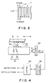
- Figure 3 is a schematic view for explaining the pattern in a portion of detecting means in Figure 2.
- Figure 4 is a schematic and diagrammatic view of a portion of Figure 2.
- Figure 5 is a flow chart for explaining semiconductor device manufacturing processes, according to an embodiment of the present invention.
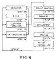
- Figure 6 is a flow chart for explaining details of a wafer process.
- Figure 7 is a perspective view of a main portion of an exposure apparatus according to another embodiment of the present invention.
- Figure 1 is a schematic view of a main portion of an exposure apparatus according to a first embodiment of the present invention.
- the invention is applied to a step-and-repeat type or step-and-scan type projection exposure apparatus for manufacture of semiconductor devices.
- Figure 2 is a schematic view for explaining a portion around a reticle 6 in Figure 1, particularly, in the case of step-and-scan method.
- the apparatus is equipped with a structure and function that, if, after relative alignment between a reticle 6 and a wafer 42 is completed, there occurs relative displacement between the reticle 6 and a reticle holding device (reticle stage) 21 therefor as a result of any influence by a change in environment or vibration or acceleration applied externally, the amount of such displacement is detected in real time by means of a linear encoder, and the position of the reticle and/or the wafer is corrected.
- the method of relative alignment between the reticle 6 and the wafer 42 will be described first.
- the relative alignment between the reticle 6 and the wafer 42 may be done in accordance with a known method, such as disclosed in Japanese Laid-Open Patent Application, Laid-Open No. 41219/1998.
- denoted at 6 is a reticle (first object) which is placed on a reticle stage 21.
- the reticle 6 can be illuminated with exposure light from illumination means 41.
- Denoted at 8a and 8b are a reticle alignment mark formed on the reticle 6 surface and another alignment mark to be used for baseline measurement.
- Denoted at 42 is a wafer (second object) having a wafer alignment mark 43 formed on its surface.
- Denoted at 44 is a projection optical system having a projection lens system, for projecting a circuit pattern, for example, formed on the reticle 6 surface onto the wafer 42 surface.
- Denoted at 50 is a ⁇ -Z stage on which the wafer 42 is placed. It serves to perform ⁇ rotation of the wafer 42 as well as focus adjustment (adjustment in Z direction) of the wafer.
- a stage reference mark 100 which is made by a Si substrate machined into a predetermined shape.
- the ⁇ -Z stage 50 is mounted on an X-Y stage 45 for performing high precision stepwise motion.
- Mounted on the X-Y stage 45 is an optical square 46 which functions to provide a reference for the stage position measurement. This optical square is monitored by a laser interferometer 47.
- the ⁇ -Z 50 and the X-Y stage 45 are components of driving means.
- the alignment procedure for the reticle 6 and the wafer 42 in this embodiment is performed indirectly, through an alignment process using a mark provided in a TTL microscope 80, to be described later.
- any relative deviation between the reference mark 64 and the reticle alignment mark 8a is detected by using a TTR (Through-The-Reticle) microscope 60 and, then, they are brought into alignment with each other.
- TTR Through-The-Reticle
- Figure 1 there is only one TTR microscope 60 illustrated, another microscope is provided on the left-hand side of the optical axis 44a of the projection optical system 44.
- rotation of the reticle 6 can be detected and, thus, further improvement of alignment precision is attainable.
- the alignment of the reticle 6 and the reference mark 64 is performed in the following manner.
- the TTR microscope 60 includes a combination of a mirror 48 and an objective lens 49a, and a mechanism (not shown) for moving them along a plane parallel to the reticle 6.
- the system from the objective lens 49a to a relay lens 69a is an afocal system.
- the mirror 48 and the objective lens 49a Prior to detection of the reference mark 64, the mirror 48 and the objective lens 49a are moved to the position for alignment of the reticle 6.
- Light from an exposure light source 41 goes through a light guide 70, and it is directed to the TTR microscope 60.
- a wavelength selecting filter 68 By means of a wavelength selecting filter 68, only a wavelength corresponding to the exposure light, in this example, is selected and directed into the TTR microscope 60.
- the wavelength selecting filter 68 By means of the wavelength selecting filter 68, only light of predetermined wavelength width is allowed to pass, and the light is collected by a condenser lens 62a and then it is reflected by a beam splitter 61.
- the light reflected by the beam splitter 61 goes via the objective lens 49a and the mirror 48, with which the reticle alignment mark 8a and the reference mark 64 are illuminated.
- the reticle alignment mark 8a of the reticle 6 and the reference mark 64 are set to be disposed with a spacing not greater than the depth of focus of the objective lens 49a.
- the light reflected by the reticle alignment mark 8a and the reference mark 64 goes back along its on-coming path, via the mirror 48 and the objective lens 49a in this order, and after passing the beam splitter 61, it is projected on a CCD 19a surface.
- mark images of these marks are formed thereon.
- a video signal as provided by photoelectric conversion through the CCD camera 19a is transmitted to an image processing device (not shown), whereby relative deviation between the reticle alignment mark 8a and the reference mark 64 is calculated.
- the reticle stage 21 is moved to bring the reticle 6 into alignment with the major assembly of the exposure apparatus.
- the alignment of a wafer 42 is performed by detecting a wafer alignment mark (mark) 43 provided on the wafer 42, by using a TTL (Through-The-Lens) microscope 80.
- a light source which comprises a white light source such as a halogen lamp, for example.
- Wavelength selecting filter 66 functions to pass therethrough only light of a predetermined wavelength width (for example, a wavelength of 633 ⁇ 20 nm and a half width of 40 nm), different from the exposure light, out of the light from the light source 63.
- the light goes through a condenser lens (illumination optical system) 62 and impinges on a polarization beam splitter 67 by which rectilinearly polarized light having a plane of polarization in a predetermined direction is reflected.
- the light reflected by the polarization beam splitter 67 is then transformed by a quarter waveplate 65 into circularly polarized light which then goes through a correcting lens 49, for correction of spherical aberration or chromatic aberration. Then, the light is reflected by a mirror M1 and enters the projection lens system 44. The light received by the projection lens system 44 is emitted thereby, to illuminate the wafer alignment mark 43 upon the wafer 42 surface.
- the position of the mark image thus formed on the CCD 19 surface is observed (measured) by using image processing means (not shown), by which the positional relation of the wafer 42 can be detected.
- image processing means not shown
- a deviation of the mark image from a reference position (reference mark) defined on the CCD 19 surface may be detected.
- the TTL microscope 80 is used to perform the wafer alignment, in the following manner.
- the X-Y stage 45 is moved to place a mark 43, of a shot with respect to which the alignment is to be performed first, below the TTL microscope 80.
- the driving coordinates for the X-Y stage 45 may be the coordinates which are set as default, or it may be the coordinates as calculated by a preceding alignment measurement operation.
- the position of the mark 43 being observed through the TTL microscope 80 is calculated.
- the X-Y stage 45 is moved toward the second alignment measurement shot position.
- alignment measurement is performed to the shots of a number being preset, and a driving grid for X-Y stage 45 in exposure operation is calculated.
- the X-Y stage 45 is then moved in accordance with the grid, and exposures of the wafer 42 are performed.
- the sampling of alignment shots within the wafer 42 may be made substantially concentric.
- baseline measurement is performed. This measurement uses a stage reference mark 100 which is provided on the X-Y stage 45.
- the alignment procedure has been described with reference to TTL off-axis alignment method using the projection optical system, the present invention is not limited to it.
- a TTL on-axis alignment method or a Non-TTL off-axis alignment method may be used similarly.
- Figure 2 is a schematic view for explaining detection of positional deviation of a reticle 6, placed on a reticle stage 21, by using a pattern (reticle mark) provided on the reticle 6.
- the laser interferometer 1 functions for measuring a position Y1
- the laser interferometer 2 functions for measuring a position Y2.
- the Y position measurement to the reticle stage 21 is made on the basis of the position Y1 and the position Y2, or of an average of the positions Y1 and Y2.
- Displacement of ⁇ is measured on the basis of a difference between positions Y1 and Y2.
- the laser interferometer 3 functions for position measurement with respect to X direction.
- Denoted at 4 and 5 are stators and movable elements, constituting a linear motor mechanism for X, Y and ⁇ drive of the reticle stage 21.
- the reticle stage 21 can be moved in Y direction, by means of the linear motor mechanism (4, 5). This enables scanning exposure.
- Denoted at 6 is a reticle
- denoted at 8a is a reticle mark (reticle alignment mark) for the reticle alignment.
- Denoted at 64 is a reticle reference mark which is provided on the reticle stage 21, for the reticle alignment.
- Denoted at 9 are reticle attracting pads for fixedly holding the reticle 6 on the reticle stage 21.
- Denoted at 10 (10a, 10b, 10c, 10d) is detecting means which constitutes a portion of linear encoder means for detecting relative displacement between the reticle 6 and the reticle stage 21. It is provided on the reticle stage 21.
- Denoted at 11 (11a, 11b, 11c, 11d) are linear encoder patterns, constituting a portion of the linear encoder for detecting relative displacement of the reticle 6 and the reticle stage 21, which are provided on the reticle side.
- Characters a, b, c and d denote linear encoder means (detecting means) each comprising a detecting device 10, a pattern 11 and a pattern 32, in this example. They are disposed at four corners of the reticle 6, in this embodiment.
- Figure 3 shows a portion of the pattern 11 for the linear encoder, which is provided on the reticle 6.
- the pattern 11 comprises a rectangular pattern having a reflective portion 11R and a nonreflective portion 11T, of linewidth 0.25 micron.
- the reticle 6 is conveyed onto the reticle stage 21 by reticle conveying means (not shown).
- the reticle 6 is then set or aligned by a reticle alignment system (not shown) and reticle alignment driving means (not shown) so that the deviation between the reticle alignment mark 8a and the reticle reference mark 64 is minimized.
- the reticle is held fixed on the reticle stage 21 by means of the reticle attracting pads 9.
- a deviation after the fixation is measured by using the reticle alignment system (not shown). The thus measured value is used as offset in position correction.
- the value of a pulse counter which is a constituent element of the linear encoder is initialized. If, thereafter, relative displacement occurs between the reticle 6 and the reticle stage 21, the amount of relative displacement is detected in real time by the linear encoder means a, b, c and d, and a corresponding signal is outputted. On the basis of a signal from the detecting means, the position of the reticle 6 and/or of the wafer 42 is corrected by using the correcting means, whereby accurate projection exposure is assured.
- Figure 4 is a schematic view of a main portion of the linear encoder means of Figure 2. It is to be noted here that the linear encoder means may be based on one of known measurement methods.
- the linear encoder produces a signal corresponding to the period of the pattern 11.
- the output signal is supplied to a phase divider 34 by which the resolution is increased.
- the reticle stage 21 and/or the wafer stage is moved to perform the position correction.
- the divider 34 operates to divide a periodic pattern of 0.5 micron into 512 elements.
- a resolving power of about 1 nm ( ⁇ 0.5 micron divided by 512) is obtained.
- the linear encoder has a high resolution with respect to a direction orthogonal to the mark, but the sensitivity decreases with respect to the remaining five axes.
- plural encoders are used.
- correction of relative displacement between the reticle and the reticle stage may be performed just before a driving signal for moving the wafer to its exposure position is applied, or it may be performed during the wafer drive. This may be selected by an operator. In a scan type projection exposure apparatus, the correction may be made during the scanning exposure.
- This embodiment is particularly effective in a step-and-scan type exposure apparatus.
- reciprocal motion of high speed and high acceleration is repeated while a reticle is being held by a reticle stage.
- the speed and acceleration of the reciprocal motion are becoming higher.
- the reticle on the other hand, the reticle and its position on the reticle stage are assured only by the holding performance of the reticle stage. Thus, there arises a problem in respect to shift between the reticle and the reticle stage.
- Figure 7 is a schematic view for explaining the structure for detecting a positional deviation of a reticle 6 placed on a reticle stage 21, by using a pattern (reticle mark) provided on the reticle 6.
- X-, Y- and ⁇ -drive actuators and stages related to these axes for the reticle stage 21.
- the reticle stage 21 can be moved in X, Y and ⁇ directions by means of corresponding actuators.
- Denoted at 6 is a reticle
- denoted at 8a is a reticle mark (reticle alignment mark) to be used for the reticle alignment.
- Denoted at 64 is a reticle reference mark which is provided at the base side of the reticle stage 21, for the reticle alignment.
- Denoted at 9 are reticle attracting pads for fixedly holding the reticle 6 on the reticle stage 21.
- Denoted at 10 (10a, 10b, 10c, 10d) is detecting means which constitutes a portion of linear encoder means for detecting relative displacement between the reticle 6 and the reticle stage 21. It is provided on the reticle stage 21.
- Denoted at 11 (11a, 11b, 11c, 11d) are linear encoder patterns, constituting a portion of the linear encoder for detecting relative displacement of the reticle 6 and the reticle stage 21, which are provided on the reticle side.
- Characters a, b, c and d denote linear encoder means (detecting means) each comprising a detecting device 10, a pattern 11 and a pattern 32, in this example. They are disposed at four corners of the reticle 6, in this embodiment.
- Figure 3 shows a portion of the pattern 11 for the linear encoder, which is provided on the reticle 6.
- the pattern 11 comprises a rectangular pattern having a reflective portion 11R and a nonreflective portion 11T, of linewidth 0.25 micron.
- the reticle 6 is conveyed onto the reticle stage 21 by reticle conveying means (not shown).
- the reticle 6 is then set or aligned by using a reticle alignment system (not shown) and the X-, Y- and ⁇ actuators shown in Figure 7, so that the deviation between the reticle alignment mark 8a and the reticle reference mark 64 is minimized.
- a deviation after the fixation is measured by using the reticle alignment system (not shown). The thus measured value is used as offset in position correction.
- the value of a pulse counter which is a constituent element of the linear encoder is initialized. If, thereafter, relative displacement occurs between the reticle 6 and the reticle stage 21, the amount of relative displacement is detected in real time by the linear encoder means a, b, c and d, and a corresponding signal is outputted. On the basis of a signal from the detecting means, the position of the reticle 6 and/or of the wafer 42 is corrected by using the correcting means, whereby accurate projection exposure is assured.
- Figure 5 is a flow chart of procedure for manufacture of microdevices such as semiconductor chips (e.g. ICs or LSIs), liquid crystal panels, or CCDs, for example.
- semiconductor chips e.g. ICs or LSIs
- liquid crystal panels e.g. LCDs
- CCDs complementary metal-oxide-semiconductors
- Step 1 is a design process for designing a circuit of a semiconductor device.
- Step 2 is a process for making a mask on the basis of the circuit pattern design.
- Step 3 is a process for preparing a wafer by using a material such as silicon.
- Step 4 is a wafer process which is called a pre-process wherein, by using the so prepared mask and wafer, circuits are practically formed on the wafer through lithography.
- Step 5 subsequent to this is an assembling step which is called a post-process wherein the wafer having been processed by step 4 is formed into semiconductor chips. This step includes assembling (dicing and bonding) process and packaging (chip sealing) process.
- Step 6 is an inspection step wherein operation check, durability check and so on for the semiconductor devices provided by step 5, are carried out. With these processes, semiconductor devices are completed and they are shipped (step 7).
- Figure 6 is a flow chart showing details of the wafer process.
- Step 11 is an oxidation process for oxidizing the surface of a wafer.
- Step 12 is a CVD process for forming an insulating film on the wafer surface.
- Step 13 is an electrode forming process for forming electrodes upon the wafer by vapor deposition.
- Step 14 is an ion implanting process for implanting ions to the wafer.
- Step 15 is a resist process for applying a resist (photosensitive material) to the wafer.
- Step 16 is an exposure process for printing, by exposure, the circuit pattern of the mask on the wafer through the exposure apparatus described above.
- Step 17 is a developing process for developing the exposed wafer.
- Step 18 is an etching process for removing portions other than the developed resist image.
- Step 19 is a resist separation process for separating the resist material remaining on the wafer after being subjected to the etching process. By repeating these processes, circuit patterns are superposedly formed on the wafer.
- a change in relative positional relationship between a reticle (first object) and a reticle stage, after completion of relative alignment between the reticle and a wafer (second object), more specifically, after completion of alignment (reticle alignment) of the reticle with respect to a reference mark provided on the major assembly of the apparatus, can be detected. Further, on the basis of the result of detection, the position of the reticle and/or the wafer can be corrected. This accomplishes an exposure apparatus and a device manufacturing method using the same, by which large integration semiconductor devices can be produced easily.
- positional information related to a holding stage for holding a first object with a transfer pattern e.g., a reticle stage
- detecting means provided on the stage. This facilitates production of large integration semiconductor devices.
Abstract
Description
- This invention relates to an exposure method and a device manufacturing method using the same. More particularly, the invention is concerned with an exposure apparatus or a projection exposure apparatus based on a proximity method, a step-and-repeat method or a step-and-scan method, for use in production of various devices such as IC, LSI, CCD, liquid crystal panel, or magnetic head, for example, wherein a fine electronic circuit pattern formed on a reticle (first object) is lithographically transferred to a wafer (second object) after they are relatively aligned.
- In projection exposure apparatuses for manufacture of semiconductor devices, improvement of precision of relative alignment between a reticle and a wafer is an important factor for enlargement of integration of the semiconductor device. Recently, an alignment precision higher than submicron order is required to meet further miniaturization of semiconductor chips.
- In reduction projection type exposure apparatuses for semiconductor device production, a circuit pattern of a reticle (first object) is projected and printed on a wafer (second object) through a projection lens system. Here, before the projection exposure, an observing system (detecting means) is used to observe the reticle surface or wafer surface to detect alignment marks of the reticle and/or the wafer. On the basis of the result of detection, positional registration (alignment) between the reticle and the wafer is made.
- Due to further miniaturization of semiconductor chips, improvement of precision of the relative alignment between a reticle and a wafer has been desired.
- In conventional exposure apparatuses, once a reticle is aligned with respect to a reference mark provided in a portion of the exposure apparatus (reticle alignment operation), the reticle is held fixed until the next alignment operation. For this reason, the position of the reticle is dependent upon the holding performance (holding precision) of a holding member (generally, a reticle stage) for holding the reticle.
- Generally, the reticle alignment is performed in response to reticle replacement. When the same reticle is used, the frequency of alignment operation differs in dependence upon the user. If therefore there occurs variation in environment or vibration or acceleration in the apparatus, for example, due to the influence thereof, there may occur a change in relative position between the reticle and the holding member therefor. In that occasion, when the pattern of the reticle is projected and printed on a wafer, the exposure position may displace or a deviation may occur during the exposure process. It causes degradation of resolving power for the pattern image.
- It is an object of the present invention to provide an exposure apparatus by which, the position of a reticle and/or a wafer can be corrected after relative alignment of the reticle and the wafer, particularly, after alignment (reticle alignment) of the reticle with respect to a reference mark provided in a portion of the major assembly of the exposure apparatus, and by which production of large integration semiconductor devices is facilitated.
- These and other objects, features and advantages of the present invention will become more apparent upon a consideration of the following description of the preferred embodiments of the present invention taken in conjunction with the accompanying drawings.
- Figure 1 is a schematic view of a main portion of an exposure apparatus according to an embodiment of the present invention.
- Figure 2 is an enlarged view of a portion of Figure 1.
- Figure 3 is a schematic view for explaining the pattern in a portion of detecting means in Figure 2.
- Figure 4 is a schematic and diagrammatic view of a portion of Figure 2.
- Figure 5 is a flow chart for explaining semiconductor device manufacturing processes, according to an embodiment of the present invention.
- Figure 6 is a flow chart for explaining details of a wafer process.
- Figure 7 is a perspective view of a main portion of an exposure apparatus according to another embodiment of the present invention.
- Figure 1 is a schematic view of a main portion of an exposure apparatus according to a first embodiment of the present invention. In this example, the invention is applied to a step-and-repeat type or step-and-scan type projection exposure apparatus for manufacture of semiconductor devices. Figure 2 is a schematic view for explaining a portion around a
reticle 6 in Figure 1, particularly, in the case of step-and-scan method. - In this embodiment, the apparatus is equipped with a structure and function that, if, after relative alignment between a
reticle 6 and awafer 42 is completed, there occurs relative displacement between thereticle 6 and a reticle holding device (reticle stage) 21 therefor as a result of any influence by a change in environment or vibration or acceleration applied externally, the amount of such displacement is detected in real time by means of a linear encoder, and the position of the reticle and/or the wafer is corrected. - The method of relative alignment between the
reticle 6 and thewafer 42 will be described first. The relative alignment between thereticle 6 and thewafer 42 may be done in accordance with a known method, such as disclosed in Japanese Laid-Open Patent Application, Laid-Open No. 41219/1998. - The alignment method will be described in detail.
- In Figure 1, denoted at 6 is a reticle (first object) which is placed on a
reticle stage 21. Thereticle 6 can be illuminated with exposure light from illumination means 41. Denoted at 8a and 8b are a reticle alignment mark formed on thereticle 6 surface and another alignment mark to be used for baseline measurement. Denoted at 42 is a wafer (second object) having awafer alignment mark 43 formed on its surface. Denoted at 44 is a projection optical system having a projection lens system, for projecting a circuit pattern, for example, formed on thereticle 6 surface onto thewafer 42 surface. - Denoted at 50 is a -Z stage on which the
wafer 42 is placed. It serves to perform rotation of thewafer 42 as well as focus adjustment (adjustment in Z direction) of the wafer. Provided on the -Z stage 50 is astage reference mark 100 which is made by a Si substrate machined into a predetermined shape. The -Z stage 50 is mounted on anX-Y stage 45 for performing high precision stepwise motion. Mounted on theX-Y stage 45 is anoptical square 46 which functions to provide a reference for the stage position measurement. This optical square is monitored by alaser interferometer 47. The -Z 50 and theX-Y stage 45 are components of driving means. - The alignment procedure for the
reticle 6 and thewafer 42 in this embodiment is performed indirectly, through an alignment process using a mark provided in aTTL microscope 80, to be described later. - First, the method of alignment for a mark (reticle alignment mark) 8a provided on the
reticle 6 and a reference mark (reticle reference mark) 64 provided on thereticle stage 21 which is a portion of the major assembly, will be described. - In this embodiment, any relative deviation between the
reference mark 64 and thereticle alignment mark 8a is detected by using a TTR (Through-The-Reticle)microscope 60 and, then, they are brought into alignment with each other. Although in Figure 1 there is only oneTTR microscope 60 illustrated, another microscope is provided on the left-hand side of theoptical axis 44a of the projectionoptical system 44. By using plural microscopes, rotation of thereticle 6 can be detected and, thus, further improvement of alignment precision is attainable. The alignment of thereticle 6 and thereference mark 64 is performed in the following manner. - The
TTR microscope 60 includes a combination of amirror 48 and an objective lens 49a, and a mechanism (not shown) for moving them along a plane parallel to thereticle 6. To this end, the system from the objective lens 49a to arelay lens 69a is an afocal system. Prior to detection of thereference mark 64, themirror 48 and the objective lens 49a are moved to the position for alignment of thereticle 6. - Light from an
exposure light source 41 goes through alight guide 70, and it is directed to theTTR microscope 60. By means of awavelength selecting filter 68, only a wavelength corresponding to the exposure light, in this example, is selected and directed into theTTR microscope 60. - By means of the
wavelength selecting filter 68, only light of predetermined wavelength width is allowed to pass, and the light is collected by acondenser lens 62a and then it is reflected by abeam splitter 61. The light reflected by thebeam splitter 61 goes via the objective lens 49a and themirror 48, with which thereticle alignment mark 8a and thereference mark 64 are illuminated. Thereticle alignment mark 8a of thereticle 6 and thereference mark 64 are set to be disposed with a spacing not greater than the depth of focus of the objective lens 49a. The light reflected by thereticle alignment mark 8a and thereference mark 64 goes back along its on-coming path, via themirror 48 and the objective lens 49a in this order, and after passing thebeam splitter 61, it is projected on aCCD 19a surface. Thus, mark images of these marks are formed thereon. With this arrangement, when both thereticle alignment mark 8a and thereference mark 64 are placed within the observation region of the objective lens 49a, both of these marks can be observed simultaneously. - A video signal as provided by photoelectric conversion through the
CCD camera 19a is transmitted to an image processing device (not shown), whereby relative deviation between thereticle alignment mark 8a and thereference mark 64 is calculated. On the basis of the thus produced information, thereticle stage 21 is moved to bring thereticle 6 into alignment with the major assembly of the exposure apparatus. - Next, the alignment of a
wafer 42 is performed by detecting a wafer alignment mark (mark) 43 provided on thewafer 42, by using a TTL (Through-The-Lens)microscope 80. - Now, the method of detecting the position of the
wafer alignment mark 43 on thewafer 42 will be described. Denoted at 63 is a light source (light source means) which comprises a white light source such as a halogen lamp, for example.Wavelength selecting filter 66 functions to pass therethrough only light of a predetermined wavelength width (for example, a wavelength of 633±20 nm and a half width of 40 nm), different from the exposure light, out of the light from thelight source 63. The light goes through a condenser lens (illumination optical system) 62 and impinges on apolarization beam splitter 67 by which rectilinearly polarized light having a plane of polarization in a predetermined direction is reflected. - The light reflected by the
polarization beam splitter 67 is then transformed by aquarter waveplate 65 into circularly polarized light which then goes through a correctinglens 49, for correction of spherical aberration or chromatic aberration. Then, the light is reflected by a mirror M1 and enters theprojection lens system 44. The light received by theprojection lens system 44 is emitted thereby, to illuminate thewafer alignment mark 43 upon thewafer 42 surface. - Light reflected by the
mark 43 on thewafer 42 surface goes back along its on-coming path, via theprojection lens system 44, the mirror M1 and the correctingoptical system 49 in this order, and it enters thequarter waveplate 65. The light passing thisquarter waveplate 65 has been transformed into rectilinearly polarized light having its plane of polarization rotated by 90 deg. as compared with the light before the transformation. Now, the light goes through thepolarization beam splitter 67 and, through arelay lens 69, it is projected on a CCD (image pickup device) 19. Thus, an image (mark image) of thewafer alignment mark 43 is formed thereon. - The position of the mark image thus formed on the
CCD 19 surface is observed (measured) by using image processing means (not shown), by which the positional relation of thewafer 42 can be detected. Here, for example, a deviation of the mark image from a reference position (reference mark) defined on theCCD 19 surface may be detected. More specifically, theTTL microscope 80 is used to perform the wafer alignment, in the following manner. - After completion of prealignment, the
X-Y stage 45 is moved to place amark 43, of a shot with respect to which the alignment is to be performed first, below theTTL microscope 80. Here, the driving coordinates for theX-Y stage 45 may be the coordinates which are set as default, or it may be the coordinates as calculated by a preceding alignment measurement operation. The position of themark 43 being observed through theTTL microscope 80 is calculated. After doing measurement to one shot in respect to two directions of X and Y directions, theX-Y stage 45 is moved toward the second alignment measurement shot position. - In this manner, alignment measurement is performed to the shots of a number being preset, and a driving grid for
X-Y stage 45 in exposure operation is calculated. TheX-Y stage 45 is then moved in accordance with the grid, and exposures of thewafer 42 are performed. Preferably, the sampling of alignment shots within thewafer 42 may be made substantially concentric. - Although in this embodiment the procedure has been described with reference to global alignment method, any other alignment method may be used.
- The alignment method has been described above and, since it is based on off-axis alignment method, baseline correction is necessary. To this end, baseline measurement is performed. This measurement uses a
stage reference mark 100 which is provided on theX-Y stage 45. - In the embodiment of Figure 1, the alignment procedure has been described with reference to TTL off-axis alignment method using the projection optical system, the present invention is not limited to it. For example, a TTL on-axis alignment method or a Non-TTL off-axis alignment method may be used similarly.
- Next, referring to Figure 2, a mechanism for detecting relative displacement between the
reticle 6 and thereticle stage 21, which may occur after completion of alignment between thereticle 6 and thewafer 46, will be explained. - Figure 2 is a schematic view for explaining detection of positional deviation of a
reticle 6, placed on areticle stage 21, by using a pattern (reticle mark) provided on thereticle 6. - Denoted in the drawing at 1, 2 and 3 are laser interferometers for measurement of the position of the
reticle stage 21. Thelaser interferometer 1 functions for measuring a position Y1, and thelaser interferometer 2 functions for measuring a position Y2. The Y position measurement to thereticle stage 21 is made on the basis of the position Y1 and the position Y2, or of an average of the positions Y1 and Y2. Displacement of is measured on the basis of a difference between positions Y1 and Y2. Thelaser interferometer 3 functions for position measurement with respect to X direction. - Denoted at 4 and 5 are stators and movable elements, constituting a linear motor mechanism for X, Y and drive of the
reticle stage 21. Thereticle stage 21 can be moved in Y direction, by means of the linear motor mechanism (4, 5). This enables scanning exposure. Denoted at 6 is a reticle, and denoted at 8a is a reticle mark (reticle alignment mark) for the reticle alignment. Denoted at 64 is a reticle reference mark which is provided on thereticle stage 21, for the reticle alignment. Denoted at 9 are reticle attracting pads for fixedly holding thereticle 6 on thereticle stage 21. - Denoted at 10 (10a, 10b, 10c, 10d) is detecting means which constitutes a portion of linear encoder means for detecting relative displacement between the
reticle 6 and thereticle stage 21. It is provided on thereticle stage 21. Denoted at 11 (11a, 11b, 11c, 11d) are linear encoder patterns, constituting a portion of the linear encoder for detecting relative displacement of thereticle 6 and thereticle stage 21, which are provided on the reticle side. - Characters a, b, c and d denote linear encoder means (detecting means) each comprising a detecting
device 10, apattern 11 and apattern 32, in this example. They are disposed at four corners of thereticle 6, in this embodiment. - Figure 3 shows a portion of the
pattern 11 for the linear encoder, which is provided on thereticle 6. Thepattern 11 comprises a rectangular pattern having a reflective portion 11R and a nonreflective portion 11T, of linewidth 0.25 micron. - In Figure 2, the
reticle 6 is conveyed onto thereticle stage 21 by reticle conveying means (not shown). Thereticle 6 is then set or aligned by a reticle alignment system (not shown) and reticle alignment driving means (not shown) so that the deviation between thereticle alignment mark 8a and thereticle reference mark 64 is minimized. Then, the reticle is held fixed on thereticle stage 21 by means of thereticle attracting pads 9. After the fixation, a deviation after the fixation is measured by using the reticle alignment system (not shown). The thus measured value is used as offset in position correction. - Here, the value of a pulse counter which is a constituent element of the linear encoder (not shown), is initialized. If, thereafter, relative displacement occurs between the
reticle 6 and thereticle stage 21, the amount of relative displacement is detected in real time by the linear encoder means a, b, c and d, and a corresponding signal is outputted. On the basis of a signal from the detecting means, the position of thereticle 6 and/or of thewafer 42 is corrected by using the correcting means, whereby accurate projection exposure is assured. - Figure 4 is a schematic view of a main portion of the linear encoder means of Figure 2. It is to be noted here that the linear encoder means may be based on one of known measurement methods.
- In Figure 4, light divergently emitted from a
light emitting device 31 disposed inside the detectingmeans 10 is transformed into a linear light beam array by ascale 32 provided with the same pitch as thepattern 11 on thereticle 6, and these light beams illuminate thepattern 11 on thereticle 6. The light is reflected by thepattern 11, by which thepattern 11 is projected on thescale 32. Here, due to relative deviation of thereticle 6 and the reticle stage 21 (geometrical overlay), the light quantity impinging on alight receiving element 33 is modulated. - In Figure 4, by using an output signal as produced in response from the
light receiving element 33, the amount of relative deviation between thereticle 6 and thereticle stage 21 is detected. The relative deviation is measured with respect to X and Y directions. - In this embodiment, as the
reticle 6 shifts in a direction (depicted by an arrow) orthogonal to the mark (pattern) 11, the linear encoder produces a signal corresponding to the period of thepattern 11. The output signal is supplied to aphase divider 34 by which the resolution is increased. Then, in cooperation with aposition counter 35 and acontrol device 36, thereticle stage 21 and/or the wafer stage is moved to perform the position correction. In the example shown in Figure 2 or 3, thedivider 34 operates to divide a periodic pattern of 0.5 micron into 512 elements. Thus, a resolving power of about 1 nm (≒ 0.5 micron divided by 512) is obtained. - In Figure 1, from an average of values measured by the encoders a and d, relative displacement in Y direction is measured. Also, from an average of values measured by the encoders c and b, relative displacement in X direction is measured. Further, from an average of the difference between the values measured by the encoders a and d and the difference between the values measured by the encoders c and d, relative displacement is calculated. There are three or more marks and linear encoders provided. The number of them, placement positions of them and directionality of them may be changed as desired, unless all of them are parallel to each other.
- The linear encoder has a high resolution with respect to a direction orthogonal to the mark, but the sensitivity decreases with respect to the remaining five axes. In this connection, as shown in Figure 1, plural encoders are used.
- With the structure of this embodiment described above, relative displacement between the
reticle 6 and thereticle stage 21 can be detected continuously. - In this embodiment, correction of relative displacement between the reticle and the reticle stage may be performed just before a driving signal for moving the wafer to its exposure position is applied, or it may be performed during the wafer drive. This may be selected by an operator. In a scan type projection exposure apparatus, the correction may be made during the scanning exposure.
- This embodiment is particularly effective in a step-and-scan type exposure apparatus. In such exposure apparatus, during the exposure operation, reciprocal motion of high speed and high acceleration is repeated while a reticle is being held by a reticle stage. In order to meet required increase of throughput, the speed and acceleration of the reciprocal motion are becoming higher. As regards the reticle, on the other hand, the reticle and its position on the reticle stage are assured only by the holding performance of the reticle stage. Thus, there arises a problem in respect to shift between the reticle and the reticle stage.
- Referring now to Figure 7, description will be made on a mechanism for detecting relative displacement between a
reticle 6 and areticle stage 21, in a step-and-repeat type apparatus, after the moment when positional alignment between thereticle 6 and awafer 46 is completed. - Figure 7 is a schematic view for explaining the structure for detecting a positional deviation of a
reticle 6 placed on areticle stage 21, by using a pattern (reticle mark) provided on thereticle 6. - In Figure 7, there are X-, Y- and -drive actuators and stages related to these axes, for the
reticle stage 21. Thereticle stage 21 can be moved in X, Y and directions by means of corresponding actuators. Denoted at 6 is a reticle, and denoted at 8a is a reticle mark (reticle alignment mark) to be used for the reticle alignment. Denoted at 64 is a reticle reference mark which is provided at the base side of thereticle stage 21, for the reticle alignment. Denoted at 9 are reticle attracting pads for fixedly holding thereticle 6 on thereticle stage 21. - Denoted at 10 (10a, 10b, 10c, 10d) is detecting means which constitutes a portion of linear encoder means for detecting relative displacement between the
reticle 6 and thereticle stage 21. It is provided on thereticle stage 21. Denoted at 11 (11a, 11b, 11c, 11d) are linear encoder patterns, constituting a portion of the linear encoder for detecting relative displacement of thereticle 6 and thereticle stage 21, which are provided on the reticle side. - Characters a, b, c and d denote linear encoder means (detecting means) each comprising a detecting
device 10, apattern 11 and apattern 32, in this example. They are disposed at four corners of thereticle 6, in this embodiment. - Figure 3 shows a portion of the
pattern 11 for the linear encoder, which is provided on thereticle 6. Thepattern 11 comprises a rectangular pattern having a reflective portion 11R and a nonreflective portion 11T, of linewidth 0.25 micron. - In Figure 7, the
reticle 6 is conveyed onto thereticle stage 21 by reticle conveying means (not shown). Thereticle 6 is then set or aligned by using a reticle alignment system (not shown) and the X-, Y- and actuators shown in Figure 7, so that the deviation between thereticle alignment mark 8a and thereticle reference mark 64 is minimized. After the reticle alignment is completed, a deviation after the fixation is measured by using the reticle alignment system (not shown). The thus measured value is used as offset in position correction. - Here, the value of a pulse counter which is a constituent element of the linear encoder (not shown), is initialized. If, thereafter, relative displacement occurs between the
reticle 6 and thereticle stage 21, the amount of relative displacement is detected in real time by the linear encoder means a, b, c and d, and a corresponding signal is outputted. On the basis of a signal from the detecting means, the position of thereticle 6 and/or of thewafer 42 is corrected by using the correcting means, whereby accurate projection exposure is assured. - While, in the foregoing embodiments, description has been made with reference to an example wherein relative shift between a reticle and a reticle stage is detected and corrected, a similar structure may be provided with respect to the wafer side to detect and correct a relative shift between a wafer and a wafer stage.
- Next, an embodiment of a semiconductor device manufacturing method which uses a projection exposure apparatus according to any one of the preceding embodiments, will be explained.
- Figure 5 is a flow chart of procedure for manufacture of microdevices such as semiconductor chips (e.g. ICs or LSIs), liquid crystal panels, or CCDs, for example.
-
Step 1 is a design process for designing a circuit of a semiconductor device.Step 2 is a process for making a mask on the basis of the circuit pattern design.Step 3 is a process for preparing a wafer by using a material such as silicon. Step 4 is a wafer process which is called a pre-process wherein, by using the so prepared mask and wafer, circuits are practically formed on the wafer through lithography.Step 5 subsequent to this is an assembling step which is called a post-process wherein the wafer having been processed by step 4 is formed into semiconductor chips. This step includes assembling (dicing and bonding) process and packaging (chip sealing) process.Step 6 is an inspection step wherein operation check, durability check and so on for the semiconductor devices provided bystep 5, are carried out. With these processes, semiconductor devices are completed and they are shipped (step 7). - Figure 6 is a flow chart showing details of the wafer process.
-
Step 11 is an oxidation process for oxidizing the surface of a wafer.Step 12 is a CVD process for forming an insulating film on the wafer surface.Step 13 is an electrode forming process for forming electrodes upon the wafer by vapor deposition.Step 14 is an ion implanting process for implanting ions to the wafer.Step 15 is a resist process for applying a resist (photosensitive material) to the wafer.Step 16 is an exposure process for printing, by exposure, the circuit pattern of the mask on the wafer through the exposure apparatus described above.Step 17 is a developing process for developing the exposed wafer.Step 18 is an etching process for removing portions other than the developed resist image.Step 19 is a resist separation process for separating the resist material remaining on the wafer after being subjected to the etching process. By repeating these processes, circuit patterns are superposedly formed on the wafer. - With these processes, high density microdevices can be manufactured.
- In accordance with the embodiments of the present invention as described hereinbefore, a change in relative positional relationship between a reticle (first object) and a reticle stage, after completion of relative alignment between the reticle and a wafer (second object), more specifically, after completion of alignment (reticle alignment) of the reticle with respect to a reference mark provided on the major assembly of the apparatus, can be detected. Further, on the basis of the result of detection, the position of the reticle and/or the wafer can be corrected. This accomplishes an exposure apparatus and a device manufacturing method using the same, by which large integration semiconductor devices can be produced easily.
- Moreover, positional information related to a holding stage for holding a first object with a transfer pattern, e.g., a reticle stage, can be detected in real time by using detecting means provided on the stage. This facilitates production of large integration semiconductor devices.
- While the invention has been described with reference to the structures disclosed herein, it is not confined to the details set forth and this application is intended to cover such modifications or changes as may come within the purposes of the improvements or the scope of the following claims.
Claims (23)
- An exposure apparatus for transferring a pattern of a first object onto a second object, comprising:a holding member for holding the first object, the first object being positioned on said holding member and then held thereon; anddetecting means for detecting a relative positional relationship between the first object and said holding member, said detecting means detecting the relative positional relationship after the first object is positioned on said holding member.
- An apparatus according to Claim 1, wherein said detecting means detects the relative positional relationship by using a mark provided on the first object and a mark provided on said holding member.
- An apparatus according to Claim 2, wherein said detecting means includes a light emitting element and a light receiving element, and wherein light from said light emitting element goes via the marks of said holding member and the first object and is received by said light receiving element.
- An apparatus according to Claim 1, wherein said detecting means is made integral with at least a portion of said holding member.
- An apparatus according to Claim 1, wherein the first object is a reticle and said holding member is a reticle stage.
- An apparatus according to Claim 1, further comprising correcting means for correcting the position of at least one of the first and second objects, on the basis of the detection by said detecting means.
- An apparatus according to Claim 1, wherein the first object as held by said holding means and the second object are aligned with each other, and wherein, after the alignment, the pattern of the first object is transferred to the second object.
- An apparatus according to Claim 7, wherein the first object is a reticle and said holding member is a reticle stage.
- An apparatus according to Claim 1, wherein said apparatus includes a first stage as said holding member, for holding the first object, and a second stage for holding the second object, wherein the first object as held by said first stage and the second object as held by said second stage are brought into alignment with each other and then the pattern of the first object is transferred to the second object.
- An apparatus according to Claim 1, wherein said detecting means is provided on said holding member, to detect the relative positional relationship of the first object and said holding member in real time.
- An apparatus according to Claim 1, wherein said detecting means includes a light emitting element and a light receiving element, provided on said holding member, and wherein light from said light emitting element goes via a mark provided on said stage for reticle and a mark provided on the reticle and is received by said light receiving element.
- An exposure method for transferring a pattern of a first object onto a second object, said method comprising the steps of:positioning the first object on a holding member and then holding the first object with the holding member; anddetecting a relative positional relationship between the first object and the holding member, after the first object is positioned on the holding member.
- A method according to Claim 12, wherein the first object as held by the holding member and the second object are brought into alignment with each other and, after the alignment, the pattern of the first object is transferred to the second object.
- A method according to Claim 12, further comprising correcting a position of at least one of the first and second objects, on the basis of said detection.
- A method according to Claim 14, wherein said correction is made before the pattern of the first object is transferred to the second object.
- A method according to Claim 14, wherein said correction is made during transfer of the pattern of the first object to the second object.
- A method according to Claim 14, wherein said correction is made before or during movement of the second object toward a position where the pattern of the first object is to be transferred to the second object.
- A method according to Claim 14, wherein said correction can be done in selected one of plural modes of operation.
- A device manufacturing method, characterized by transferring a pattern of a first object onto a second object by use of an exposure apparatus as recited in any one of Claims 1 - 11, and manufacturing a device from the patterned second object.
- A device manufacturing method, characterized by transferring a pattern of a first object onto a second object by use of an exposure method as recited in any one of Claims 12 - 18, and manufacturing a device from the patterned second object.
- An exposure apparatus for transferring a pattern of a first object onto a second object, comprising:a first holding member for holding the first object;a second holding member for holding the second object; anddetecting means for detecting a relative positional relationship between at least one of the first and the second object and its respective holding means.
- An exposure apparatus according to claim 21 wherein said detecting means comprises a mark on the said at least one of the first or second objects and a mark on the respective holding means.
- An exposure method for transferring a pattern from a first object onto a second object, including the steps of:positioning the first object on a first holding means;positioning the second object on a second holding means;detecting a relative positional relationship between at least one of the first and second objects and its respective holding means;aligning the first and second objects; andexposing the first object to project a pattern onto the second object.
Applications Claiming Priority (2)
| Application Number | Priority Date | Filing Date | Title |
|---|---|---|---|
| JP18169898 | 1998-06-12 | ||
| JP10181698A JP2000003855A (en) | 1998-06-12 | 1998-06-12 | Aligner and manufacture of device using the same |
Publications (2)
| Publication Number | Publication Date |
|---|---|
| EP0964308A2 true EP0964308A2 (en) | 1999-12-15 |
| EP0964308A3 EP0964308A3 (en) | 2001-03-14 |
Family
ID=16105308
Family Applications (1)
| Application Number | Title | Priority Date | Filing Date |
|---|---|---|---|
| EP99304577A Withdrawn EP0964308A3 (en) | 1998-06-12 | 1999-06-11 | Exposure method and apparatus and device manufacturing method using the same |
Country Status (4)
| Country | Link |
|---|---|
| US (1) | US6714691B2 (en) |
| EP (1) | EP0964308A3 (en) |
| JP (1) | JP2000003855A (en) |
| KR (1) | KR100294427B1 (en) |
Cited By (3)
| Publication number | Priority date | Publication date | Assignee | Title |
|---|---|---|---|---|
| EP1260871A2 (en) * | 2001-05-22 | 2002-11-27 | Canon Kabushiki Kaisha | Position detecting method and apparatus, exposure apparatus and device manufacturing method |
| EP1308789A2 (en) | 2001-10-30 | 2003-05-07 | Canon Kabushiki Kaisha | Alignment apparatus, exposure apparatus using same, and method of manufacturing devices |
| CN111258183A (en) * | 2018-11-30 | 2020-06-09 | 佳能株式会社 | Lithographic apparatus, method of determining and method of manufacturing an article |
Families Citing this family (9)
| Publication number | Priority date | Publication date | Assignee | Title |
|---|---|---|---|---|
| JP4803901B2 (en) * | 2001-05-22 | 2011-10-26 | キヤノン株式会社 | Alignment method, exposure apparatus, and semiconductor device manufacturing method |
| US7714981B2 (en) * | 2006-10-30 | 2010-05-11 | Asml Netherlands B.V. | Lithographic apparatus and method |
| DE102008011761A1 (en) * | 2007-03-13 | 2008-09-18 | Carl Zeiss Smt Ag | Adjustment device for micro lithographic-projection illumination system, has auto collimation unit permitting adjustment accuracy, which is greater than specified value, where collimation unit is provided with light source and reflector |
| NL1036028A1 (en) | 2007-10-09 | 2009-04-15 | Asml Netherlands Bv | Servo control system, lithographic apparatus and control method. |
| NL2003529A (en) * | 2008-10-24 | 2010-04-27 | Asml Netherlands Bv | Lithographic apparatus, device manufacturing method and position control method. |
| JP5832345B2 (en) * | 2012-03-22 | 2015-12-16 | 株式会社ニューフレアテクノロジー | Inspection apparatus and inspection method |
| CN102743134B (en) * | 2012-07-30 | 2014-11-05 | 苏州诚河清洁设备有限公司 | Steam cleaning equipment |
| WO2017021131A1 (en) * | 2015-07-31 | 2017-02-09 | Asml Holding N.V. | Optical system of an alignment system |
| US11867501B2 (en) * | 2021-12-28 | 2024-01-09 | Mloptic Corp. | Integrated calibration tool for optical instrument entrance pupil 6-axis spatial allocation |
Citations (4)
| Publication number | Priority date | Publication date | Assignee | Title |
|---|---|---|---|---|
| JPH09171246A (en) * | 1995-12-19 | 1997-06-30 | Nikon Corp | Mask substrate, mask substrate attachable projection aligner and formation of pattern using it |
| JPH1041219A (en) * | 1996-07-17 | 1998-02-13 | Canon Inc | Projection aligner and manufacturing of device using it |
| JPH1050604A (en) * | 1996-04-04 | 1998-02-20 | Nikon Corp | Method for controlling position and method for alignment |
| NL1011888C2 (en) * | 1998-04-27 | 2000-01-07 | Fujitsu Ltd | Stepper having a reticle and a method of positioning a reticle in a stepper, a manufacturing process of a semiconductor device using such a stepper. |
Family Cites Families (15)
| Publication number | Priority date | Publication date | Assignee | Title |
|---|---|---|---|---|
| US4780615A (en) * | 1985-02-01 | 1988-10-25 | Canon Kabushiki Kaisha | Alignment system for use in pattern transfer apparatus |
| US5231471A (en) * | 1986-03-25 | 1993-07-27 | Canon Kabushiki Kaisha | Alignment and exposure apparatus |
| JPH02292813A (en) * | 1989-05-02 | 1990-12-04 | Canon Inc | Automatic focussing device |
| US5151749A (en) * | 1989-06-08 | 1992-09-29 | Nikon Corporation | Method of and apparatus for measuring coordinate position and positioning an object |
| JPH0513297A (en) * | 1991-07-09 | 1993-01-22 | Nikon Corp | Aligning apparatus |
| US5978071A (en) * | 1993-01-07 | 1999-11-02 | Nikon Corporation | Projection exposure apparatus and method in which mask stage is moved to provide alignment with a moving wafer stage |
| JPH07226357A (en) * | 1993-12-16 | 1995-08-22 | Nikon Corp | Position detecting device |
| JP3186011B2 (en) | 1994-06-24 | 2001-07-11 | キヤノン株式会社 | Projection exposure apparatus and device manufacturing method |
| KR100246574B1 (en) * | 1994-12-26 | 2000-03-15 | 유무성 | Reticle alignment method |
| JP3819048B2 (en) * | 1995-03-15 | 2006-09-06 | 株式会社ニコン | Projection optical system, exposure apparatus including the same, and exposure method |
| US5751404A (en) * | 1995-07-24 | 1998-05-12 | Canon Kabushiki Kaisha | Exposure apparatus and method wherein alignment is carried out by comparing marks which are incident on both reticle stage and wafer stage reference plates |
| JPH1012544A (en) * | 1996-06-26 | 1998-01-16 | Nikon Corp | Position-measuring method and exposure method |
| US5917580A (en) * | 1996-08-29 | 1999-06-29 | Canon Kabushiki Kaisha | Scan exposure method and apparatus |
| JP3531894B2 (en) * | 1996-09-13 | 2004-05-31 | キヤノン株式会社 | Projection exposure equipment |
| US6490025B1 (en) * | 1997-03-17 | 2002-12-03 | Nikon Corporation | Exposure apparatus |
-
1998
- 1998-06-12 JP JP10181698A patent/JP2000003855A/en active Pending
-
1999
- 1999-06-09 US US09/328,797 patent/US6714691B2/en not_active Expired - Fee Related
- 1999-06-11 EP EP99304577A patent/EP0964308A3/en not_active Withdrawn
- 1999-06-12 KR KR1019990021954A patent/KR100294427B1/en not_active IP Right Cessation
Patent Citations (4)
| Publication number | Priority date | Publication date | Assignee | Title |
|---|---|---|---|---|
| JPH09171246A (en) * | 1995-12-19 | 1997-06-30 | Nikon Corp | Mask substrate, mask substrate attachable projection aligner and formation of pattern using it |
| JPH1050604A (en) * | 1996-04-04 | 1998-02-20 | Nikon Corp | Method for controlling position and method for alignment |
| JPH1041219A (en) * | 1996-07-17 | 1998-02-13 | Canon Inc | Projection aligner and manufacturing of device using it |
| NL1011888C2 (en) * | 1998-04-27 | 2000-01-07 | Fujitsu Ltd | Stepper having a reticle and a method of positioning a reticle in a stepper, a manufacturing process of a semiconductor device using such a stepper. |
Non-Patent Citations (3)
| Title |
|---|
| PATENT ABSTRACTS OF JAPAN vol. 1997, no. 10, 31 October 1997 (1997-10-31) -& JP 09 171246 A (NIKON CORP), 30 June 1997 (1997-06-30) -& US 5 894 056 A (UMATATE TOSHIKAZU) 13 April 1999 (1999-04-13) * |
| PATENT ABSTRACTS OF JAPAN vol. 1998, no. 06, 30 April 1998 (1998-04-30) -& JP 10 041219 A (CANON INC), 13 February 1998 (1998-02-13) * |
| PATENT ABSTRACTS OF JAPAN vol. 1998, no. 06, 30 April 1998 (1998-04-30) -& JP 10 050604 A (NIKON CORP), 20 February 1998 (1998-02-20) -& US 6 141 108 A (KIDA YOSHIKI ET AL) 31 October 2000 (2000-10-31) * |
Cited By (9)
| Publication number | Priority date | Publication date | Assignee | Title |
|---|---|---|---|---|
| EP1260871A2 (en) * | 2001-05-22 | 2002-11-27 | Canon Kabushiki Kaisha | Position detecting method and apparatus, exposure apparatus and device manufacturing method |
| EP1260871A3 (en) * | 2001-05-22 | 2006-04-12 | Canon Kabushiki Kaisha | Position detecting method and apparatus, exposure apparatus and device manufacturing method |
| US7148973B2 (en) | 2001-05-22 | 2006-12-12 | Canon Kabushiki Kaisha | Position detecting method and apparatus, exposure apparatus and device manufacturing method |
| EP1308789A2 (en) | 2001-10-30 | 2003-05-07 | Canon Kabushiki Kaisha | Alignment apparatus, exposure apparatus using same, and method of manufacturing devices |
| EP1308789A3 (en) * | 2001-10-30 | 2006-04-12 | Canon Kabushiki Kaisha | Alignment apparatus, exposure apparatus using same, and method of manufacturing devices |
| US7173716B2 (en) | 2001-10-30 | 2007-02-06 | Canon Kabushiki Kaisha | Alignment apparatus, exposure apparatus using the same, and method of manufacturing devices |
| CN111258183A (en) * | 2018-11-30 | 2020-06-09 | 佳能株式会社 | Lithographic apparatus, method of determining and method of manufacturing an article |
| EP3667423A1 (en) * | 2018-11-30 | 2020-06-17 | Canon Kabushiki Kaisha | Lithography apparatus, determination method, and method of manufacturing an article |
| US11275319B2 (en) | 2018-11-30 | 2022-03-15 | Canon Kabushiki Kaisha | Lithography apparatus, determination method, and method of manufacturing an article |
Also Published As
| Publication number | Publication date |
|---|---|
| US6714691B2 (en) | 2004-03-30 |
| KR20000006140A (en) | 2000-01-25 |
| KR100294427B1 (en) | 2001-07-12 |
| US20030048960A1 (en) | 2003-03-13 |
| EP0964308A3 (en) | 2001-03-14 |
| JP2000003855A (en) | 2000-01-07 |
Similar Documents
| Publication | Publication Date | Title |
|---|---|---|
| US5751404A (en) | Exposure apparatus and method wherein alignment is carried out by comparing marks which are incident on both reticle stage and wafer stage reference plates | |
| US6529625B2 (en) | Position detecting method and position detecting device for detecting relative positions of objects having position detecting marks by using separate reference member having alignment marks | |
| US6714691B2 (en) | Exposure method and apparatus, and device manufacturing method using the same | |
| US20030038937A1 (en) | Projection exposure apparatus and device manufacturing method using the same | |
| JPH09199406A (en) | Position detecting device and manufacture of semiconductor element using thereof | |
| US6268902B1 (en) | Exposure apparatus, and manufacturing method for devices using same | |
| US5745242A (en) | Position detecting system and exposure apparatus having the same | |
| EP1098360A1 (en) | Position sensing method, position sensor, exposure method, exposure apparatus, and production process thereof, and device and device manufacturing method | |
| US20010023918A1 (en) | Alignment apparatus, alignment method, exposure apparatus and exposure method | |
| US6233042B1 (en) | Projection exposure apparatus and device manufacturing method using the same | |
| US6683673B2 (en) | Alignment system and projection exposure apparatus | |
| US6069683A (en) | Scanning exposure method and apparatus | |
| JP3335126B2 (en) | Surface position detecting apparatus and scanning projection exposure apparatus using the same | |
| US7313873B2 (en) | Surface position measuring method, exposure apparatus, and device manufacturing method | |
| JP3441930B2 (en) | Scanning exposure apparatus and device manufacturing method | |
| US5999270A (en) | Projection exposure apparatus and microdevice manufacturing method using the same | |
| JP2005175383A (en) | Aligner, method of alignment and device manufacturing method | |
| JPH11176745A (en) | Position detection device and aligner using the same | |
| JPH1154416A (en) | Projection aligner and manufacture thereof | |
| JP2002139847A (en) | Aligner, exposing method and device manufacturing method | |
| JPH10335239A (en) | Exposure method and system | |
| JPH1050594A (en) | Aligner and projection aligner using the same | |
| JPH113930A (en) | Alignment method and device | |
| JP2000353655A (en) | Position detecting mark, mark detecting device using the same, and aligner | |
| JPH0992592A (en) | Scan exposure system and manufacture of device thereby |
Legal Events
| Date | Code | Title | Description |
|---|---|---|---|
| PUAI | Public reference made under article 153(3) epc to a published international application that has entered the european phase |
Free format text: ORIGINAL CODE: 0009012 |
|
| AK | Designated contracting states |
Kind code of ref document: A2 Designated state(s): DE GB NL |
|
| AX | Request for extension of the european patent |
Free format text: AL;LT;LV;MK;RO;SI |
|
| PUAL | Search report despatched |
Free format text: ORIGINAL CODE: 0009013 |
|
| AK | Designated contracting states |
Kind code of ref document: A3 Designated state(s): AT BE CH CY DE DK ES FI FR GB GR IE IT LI LU MC NL PT SE |
|
| AX | Request for extension of the european patent |
Free format text: AL;LT;LV;MK;RO;SI |
|
| 17P | Request for examination filed |
Effective date: 20010727 |
|
| AKX | Designation fees paid |
Free format text: DE GB NL |
|
| 17Q | First examination report despatched |
Effective date: 20011105 |
|
| STAA | Information on the status of an ep patent application or granted ep patent |
Free format text: STATUS: THE APPLICATION HAS BEEN WITHDRAWN |
|
| 18W | Application withdrawn |
Effective date: 20100125 |