EP0964521A2 - Logic module with configurable combinational and sequential blocks - Google Patents
Logic module with configurable combinational and sequential blocks Download PDFInfo
- Publication number
- EP0964521A2 EP0964521A2 EP99117182A EP99117182A EP0964521A2 EP 0964521 A2 EP0964521 A2 EP 0964521A2 EP 99117182 A EP99117182 A EP 99117182A EP 99117182 A EP99117182 A EP 99117182A EP 0964521 A2 EP0964521 A2 EP 0964521A2
- Authority
- EP
- European Patent Office
- Prior art keywords
- input
- output
- multiplexer
- data
- logic
- Prior art date
- Legal status (The legal status is an assumption and is not a legal conclusion. Google has not performed a legal analysis and makes no representation as to the accuracy of the status listed.)
- Granted
Links
Images

Classifications
-
- H—ELECTRICITY
- H03—ELECTRONIC CIRCUITRY
- H03K—PULSE TECHNIQUE
- H03K19/00—Logic circuits, i.e. having at least two inputs acting on one output; Inverting circuits
- H03K19/02—Logic circuits, i.e. having at least two inputs acting on one output; Inverting circuits using specified components
- H03K19/173—Logic circuits, i.e. having at least two inputs acting on one output; Inverting circuits using specified components using elementary logic circuits as components
- H03K19/1733—Controllable logic circuits
- H03K19/1737—Controllable logic circuits using multiplexers
-
- H—ELECTRICITY
- H03—ELECTRONIC CIRCUITRY
- H03K—PULSE TECHNIQUE
- H03K3/00—Circuits for generating electric pulses; Monostable, bistable or multistable circuits
- H03K3/02—Generators characterised by the type of circuit or by the means used for producing pulses
- H03K3/027—Generators characterised by the type of circuit or by the means used for producing pulses by the use of logic circuits, with internal or external positive feedback
- H03K3/037—Bistable circuits
Abstract
Description
- The present invention relates to digital electronic circuits. More specifically, the present invention relates to circuits for performing logic functions in user-programmable integrated circuits, and to circuits for implementing a wide variety of user-selectable sequential logic functions.
- Programmable logic blocks which are capable of performing a selectable one of a plurality of user-selectable logic functions are known in the prior art. U.S. Patent No. 4,910,417 to El Ganal et al., assigned to the same assignee as the present invention, and U.S. Patent No. 4,453,096 to Le Can et al., disclose logic modules composed of multiplexers capable of performing a plurality of combinatorial functions.
- L'Onde Electrique Vol. 59, No. 11, pp 81-86 describes a universal combinatorial logic module using 3 multiplexers.
- While these circuits provide a degree of flexibility to the designer of user-programmable logic arrays, there is always a need for improvement of functionality of such circuits.
- JP-A-1,093,918 discloses a latching device having the features of the preamble of appended
claim 1. - The present invention is defined in appended
claim 1 . - In an embodiment of the present invention, a logic module is provided having a wide variety of user-configurable sequential logic functions.
- In a first stage of a sequential section of the logic module of the present invention, the output of the third two-input multiplexer is connected to a first data input of a fourth two-input multiplexer having a HOLD1 input coupled to its select input. Its output and a low active CLEAR input are presented to an AND gate whose output is connected to the second data input of the fourth two-input multiplexer and to the first data input of a fifth two-input multiplexer in a second stage of the sequential section of the logic module of the present invention. The select input of the fifth two-input multiplexer is connected to a HOLD2 input. Its output and the CLEAR input are presented to an AND gate whose output is connected to the second data input of the fifth two-input multiplexer and to an output node. The CLEAR, HOLD1 and HOLD2 inputs are defined by combinations of signals from a data signal of a third group which may contain a data signal of one of the other groups.
- The invention will be described below with reference to an exemplary embodiment and the accompanying drawings, in which:
- FIG. 1 is a block diagram of a logic nodule according to a presently preferred embodiment of the present invention.
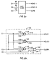
- FIG. 2a is a diagram showing a combinatorial circuit for generating the CLEAR, HOLD1, and HOLD2 signals for the circuit of FIG. 1 from data inputs.
- FIG. 2b is a logic diagram in block form of a presently preferred circuit for use in performing the function of the circuit of FIG. 2a.
-
- Referring first to FIG. 1, a block diagram of a presently preferred embodiment of a logic module according to the present invention, a
logic nodule 10 is shown having configurable combinational and sequential blocks. The combinatorial portion of the logic nodule includes first and second sections. A first section of thelogic module 10 of the present invention includes first and second two-input multiplexers second data inputs input 20 andoutput 22. Second two-input multiplexer has first andsecond data inputs input 28 andoutput 30. Selectinputs input multiplexers output 32 of a two-input logic gate of afirst type 34 having first and second data inputs 50 and 54. -
Outputs input multiplexers data inputs input multiplexer 40, in a second section oflogic module 10. Third two-input multiplexer 40 also includesselect input 42 andoutput 44. Selectinput 42 of third two-input multiplexer 40 is connected tooutput 46 of a two-input logic gate of asecond type 48 having first andsecond data inputs - The
data inputs logic gates 34 and 48 (reference numerals 50 and 52, respectively) is sourced from a data signal of a second group shown in FIG. 1 as data input nodes A0 and A1, respectively, and the other input of each of the logic gates (reference numerals 54 and 56, respectively) is sourced from a data signal of a third group shown in FIG. 1 as data input nodes B0 and B1, respectively. - The
logic module 10 of the present invention offers a plurality of combinatorial functions having up to eight inputs. The function implemented by the circuit of FIG. 1 is: - The combinatorial functions which may be implemented include AND, OR, NAND, NOR, and EX-OR. TABLE I shows the implementation of these functions using different inputs of the circuit of FIG. 1.
FUNCTION A0 B0 A1 B1 D00 D01 D10 D11 C1 C2 NAND !(A·B) A B 1 X X X 1 0 1 0 A B X 1 X X 1 0 1 0 A B 0 0 1 0 X X 1 0 A B 0 0 1 0 0 0 1 0 1 A 0 B 1 1 1 0 1 0 1 A B 0 1 1 1 0 1 0 A 1 0 B 1 1 1 0 1 0 A 1 B 0 1 1 1 0 1 0 NOR !(A+B) 1 1 A B X 1 X 0 1 0 0 X A B X X 0 X 1 0 X 0 A B X X 0 X 1 0 1 A 0 B 1 0 0 0 1 0 1 A B 0 1 0 0 0 1 0 A 1 0 B 1 0 0 0 1 0 A 1 B 0 1 0 0 0 1 0 AND (A·B) A B 0 0 0 1 X X 1 0 A B 1 X X X 0 1 1 0 A B X 1 X X 0 1 1 0 A B 0 0 0 0 1 0 1 0 1 A B 0 0 0 0 1 1 0 1 A 0 B 0 0 0 0 1 0 A 1 B 0 0 0 0 1 1 0 A 1 0 B 0 0 0 1 1 0 OR (A+B) X X A B 0 0 1 1 1 0 0 X A B 0 X 1 X 1 0 X 0 A B 0 X 1 X 1 0 1 A 0 B 0 1 1 1 1 0 1 A B 0 0 1 1 1 1 0 A 1 0 B 0 1 1 1 1 0 A 1 B 0 0 1 1 1 1 0 XOR (A·!B)+(!A·B) A 1 B 0 0 1 1 0 1 0 A 1 0 B 0 1 1 0 1 0 1 A B 0 0 1 1 0 1 0 1 A 0 B 0 1 1 0 1 0 XNOR (A·B)+(!A·!B) A 1 B 0 1 0 0 1 1 0 A 1 0 B 1 0 0 1 1 0 1 A B 0 1 0 0 1 1 0 1 A 0 B 1 0 0 1 1 0 - Those of ordinary skill in the art will further appreciate that different gates, such as NAND, NOR, EX-OR gates, could be used as well with slightly different results. In particular, using all like gates on the select inputs (for example, all NAND or NOR gates), increases the number of inputs on the functions (AND OR), while using a mix of gates on the select inputs (for example NAND on the first select input and NOR on the second select input as shown in FIG. 1) increases the number of functions which the module can generate.
- Referring again to FIG. 1, it may be seen that the sequential portion of
logic module 10 also has two stages. In the first sequential stage, theoutput 44 of the third two-input multiplexer 40 is connected to afirst data input 58 of a fourth two-input multiplexer 60 having itsselect input 62 driven by a HOLD1 signal from a HOLD1 control node. Itsoutput 64 and a CLEAR signal from a CLEAR control node are presented toinputs AND gate 70 whoseoutput 72 is connected to thesecond data input 74 of the fourth two-input multiplexer and to thefirst data input 76 of a fifth two-input multiplexer 78, which forms the input to the second sequential stage. Theselect input 80 of the fifth two-input multiplexer 78 is connected to a HOLD2 signal from a HOLD2 control node.Output 82 of fifth two-input multiplexer 78 and the CLEAR signal are presented toinputs AND gate 88 whoseoutput 90 is connected to thesecond data input 92 of the fifth two-input multiplexer and to anoutput node 94. - In a presently preferred embodiment, the CLEAR, HOLD1 and HOLD2 signals are derived by combinatorial logic from a set of data input signals. As is shown in FIG. 2a, data signals from data input nodes C1, C2 and B0 are presented to
inputs logic combining circuit 102, which has control node outputs upon which the HOLD1, HOLD2, and CLEAR signals appear, respectively. - The
logic combining circuit 102 of FIG. 2a may be any logic circuit for combining the three inputs in a manner which produces outputs for the HOLD1, HOLD2, and CLEAR signals as set forth in the truth table in TABLE II.C1 C2 HOLD1 HOLD2 CLRB 0 0 0 1 B0 0 1 1 0 B0 1 0 0 0 1 1 1 0 1 B0 - FIG. 2b is a logic diagram of a presently preferred embodiment of such a circuit. Referring now to FIG. 2b,
logic combining circuit 102 includes ANDgate 104 with invertinginput 106 andnon-inverting input 108, andoutput 110, ANDgate 112 with invertinginput 114 andnoninverting input 116 and output 118, EXNORgate 120 withinputs output 126 and ORgate 128 withinputs output 134.C1 input 96 is connected toinputs gates EXNOR gate 120.C2 input 98 is connected toinputs gates EXNOR gate 120.B0 input 100 is connected to input 132 ofOR gate 128. Theoutput 112 of ANDgate 112 is connected to input 130 ofOR gate 128. Theoutput 110 of ANDgate 104 is the HOLD1 signal, theoutput 126 ofEXNOR gate 120 is the HOLD2 signal, and theoutput 134 ofOR gate 128 is the clear signal. - The sequential portion of the logic module of the present invention disclosed herein is configurable as a rising or falling edge flip flop with asynchronous low active clear, a transparent low or high latch with asynchronous low active clear, or as a transparent flow-through element which allows only the combinatorial section of the module to be used. All latches and flip flops are non-inverting.
- TABLE III illustrates the sequential functions available from the logic module of the present invention. From TABLE III, it can be seen that the sequential functions which may be performed include a negative triggered latch with low active clear, a positive triggered latch with low active clear, a negative triggered flip flop with low active clear, a positive triggered flip flop with low active clear and a flow through mode. As can be seen from FIG. 4, the states of inputs A0, D00 and D10 are restricted for positive and negative triggered latches. A0 must equal 1 and both D00 and D10 must equal 0 in order for the output to be low when the latch is in transparent node and the clear input is active.
C1 C2 FUNCTION !CLEAR RESTRICTIONS 0 CLK Rising Edge Flip Flop B0 None CLK 1 Falling Edge Flip Flop B0 None 1 CLK High Latch with Clear B0 A0=1; D00,D10=0 CLK 0 Low Latch with Clear B0 A0=1; D00,D10=0 1 CLK High Latch -- B0=1 CLK 0 Low latch -- B0=1 1 0 Transparent -- None - The two-input multiplexers and other logic components of the logic module of the present invention may be fabricated using conventional MOS and CMOS technology.
- While presently-preferred embodiments of the present invention have been disclosed herein, those of ordinary skill in the art will be enabled, from the within disclosure, to configure embodiments which although not expressly disclosed herein nevertheless fall within the scope of the present invention. It is therefore, the intent of the inventors that the scope of the present invention be limited only by the appended claims.
Claims (1)
- A universal sequential logic module including:a first multiplexer (60) having a first data input (58) connected to a first data input node, a second data input (74), a select input (62) connected to a first control node, and an output (64), anda first AND gate (70) having a first data input (68) connected to the output of said first multiplexer (60), a second data input (66) connected to a second control node (CLA3), and an output (32) connected to the second input (74) of said first multiplexer (60), characterised by:a second multiplexer (78) having a first data input (76) connected to the output of said first AND gate (70), a second data input (92), a select input (80) connected to a third control node, and an output (87),a second AND gate (88) having a first input (86) connected to the output of said second multiplexer (78), a second input (84) connected to said second control node (CLA3), and an output (90) connected to the second input (92) of said second multiplexer and to an output node,first combinational means (102) for placing either a logic zero or a logic one on said second control node (CLA3) in response to preselected combinations of the states of a second (1), a third (2) and a fourth (30) data input node, andsecond combinational means (102) for placing either a logic zero or a logic one on said first control node and for placing either a logic zero or a logic one on said third control node in response to preselected combinations of the states of said third (12) and fourth data input nodes (80).
Applications Claiming Priority (4)
| Application Number | Priority Date | Filing Date | Title |
|---|---|---|---|
| US522232 | 1990-05-11 | ||
| US07/522,232 US5055718A (en) | 1990-05-11 | 1990-05-11 | Logic module with configurable combinational and sequential blocks |
| EP96116903A EP0756382A3 (en) | 1990-05-11 | 1991-04-30 | Logic module with configurable combinational and sequential blocks |
| EP91303916A EP0456399B1 (en) | 1990-05-11 | 1991-04-30 | Logic module with configurable combinational and sequential blocks |
Related Parent Applications (1)
| Application Number | Title | Priority Date | Filing Date |
|---|---|---|---|
| EP96116903A Division EP0756382A3 (en) | 1990-05-11 | 1991-04-30 | Logic module with configurable combinational and sequential blocks |
Publications (3)
| Publication Number | Publication Date |
|---|---|
| EP0964521A2 true EP0964521A2 (en) | 1999-12-15 |
| EP0964521A3 EP0964521A3 (en) | 1999-12-22 |
| EP0964521B1 EP0964521B1 (en) | 2005-01-12 |
Family
ID=24080033
Family Applications (3)
| Application Number | Title | Priority Date | Filing Date |
|---|---|---|---|
| EP96116903A Withdrawn EP0756382A3 (en) | 1990-05-11 | 1991-04-30 | Logic module with configurable combinational and sequential blocks |
| EP91303916A Expired - Lifetime EP0456399B1 (en) | 1990-05-11 | 1991-04-30 | Logic module with configurable combinational and sequential blocks |
| EP99117182A Expired - Lifetime EP0964521B1 (en) | 1990-05-11 | 1991-04-30 | Logic module with configurable combinational and sequential blocks |
Family Applications Before (2)
| Application Number | Title | Priority Date | Filing Date |
|---|---|---|---|
| EP96116903A Withdrawn EP0756382A3 (en) | 1990-05-11 | 1991-04-30 | Logic module with configurable combinational and sequential blocks |
| EP91303916A Expired - Lifetime EP0456399B1 (en) | 1990-05-11 | 1991-04-30 | Logic module with configurable combinational and sequential blocks |
Country Status (5)
| Country | Link |
|---|---|
| US (1) | US5055718A (en) |
| EP (3) | EP0756382A3 (en) |
| JP (1) | JPH07106949A (en) |
| AT (2) | ATE155298T1 (en) |
| DE (2) | DE69126741T2 (en) |
Families Citing this family (48)
| Publication number | Priority date | Publication date | Assignee | Title |
|---|---|---|---|---|
| US5477165A (en) * | 1986-09-19 | 1995-12-19 | Actel Corporation | Programmable logic module and architecture for field programmable gate array device |
| US5451887A (en) | 1986-09-19 | 1995-09-19 | Actel Corporation | Programmable logic module and architecture for field programmable gate array device |
| US5198705A (en) | 1990-05-11 | 1993-03-30 | Actel Corporation | Logic module with configurable combinational and sequential blocks |
| US5185539A (en) * | 1990-08-31 | 1993-02-09 | Motorola, Inc. | Programmable logic device address buffer/multiplexer/driver |
| US5680318A (en) * | 1990-12-21 | 1997-10-21 | Synopsys Inc. | Synthesizer for generating a logic network using a hardware independent description |
| US5416367A (en) * | 1991-03-06 | 1995-05-16 | Quicklogic Corporation | Programmable application specific integrated circuit and logic cell therefor |
| US5122685A (en) * | 1991-03-06 | 1992-06-16 | Quicklogic Corporation | Programmable application specific integrated circuit and logic cell therefor |
| US5220213A (en) * | 1991-03-06 | 1993-06-15 | Quicklogic Corporation | Programmable application specific integrated circuit and logic cell therefor |
| US5322812A (en) | 1991-03-20 | 1994-06-21 | Crosspoint Solutions, Inc. | Improved method of fabricating antifuses in an integrated circuit device and resulting structure |
| JP3359932B2 (en) * | 1991-05-10 | 2002-12-24 | 株式会社東芝 | Programmable logic unit circuit and programmable logic circuit |
| US5287017A (en) * | 1992-05-15 | 1994-02-15 | Micron Technology, Inc. | Programmable logic device macrocell with two OR array inputs |
| US5331227A (en) * | 1992-05-15 | 1994-07-19 | Micron Semiconductor, Inc. | Programmable logic device macrocell with an exclusive feedback line and an exclusive external input line |
| US5300830A (en) * | 1992-05-15 | 1994-04-05 | Micron Semiconductor, Inc. | Programmable logic device macrocell with an exclusive feedback and exclusive external input lines for registered and combinatorial modes using a dedicated product term for control |
| US5384500A (en) * | 1992-05-15 | 1995-01-24 | Micron Semiconductor, Inc. | Programmable logic device macrocell with an exclusive feedback and an exclusive external input line for a combinatorial mode and accommodating two separate programmable or planes |
| GB2267613B (en) * | 1992-06-02 | 1996-01-03 | Plessey Semiconductors Ltd | Programmable logic cell |
| US5298803A (en) * | 1992-07-15 | 1994-03-29 | Micron Semiconductor, Inc. | Programmable logic device having low power microcells with selectable registered and combinatorial output signals |
| US5349250A (en) * | 1993-09-02 | 1994-09-20 | Xilinx, Inc. | Logic structure and circuit for fast carry |
| US5729468A (en) * | 1994-04-21 | 1998-03-17 | Quicklogic Corporation | Reducing propagation delays in a programmable device |
| EP0707721B1 (en) * | 1994-05-04 | 2002-01-30 | Atmel Corporation | Programmable logic device with regional and universal signal routing |
| US5424655A (en) * | 1994-05-20 | 1995-06-13 | Quicklogic Corporation | Programmable application specific integrated circuit employing antifuses and methods therefor |
| US5552720A (en) * | 1994-12-01 | 1996-09-03 | Quicklogic Corporation | Method for simultaneous programming of multiple antifuses |
| US5495181A (en) * | 1994-12-01 | 1996-02-27 | Quicklogic Corporation | Integrated circuit facilitating simultaneous programming of multiple antifuses |
| US5631578A (en) * | 1995-06-02 | 1997-05-20 | International Business Machines Corporation | Programmable array interconnect network |
| US5652529A (en) * | 1995-06-02 | 1997-07-29 | International Business Machines Corporation | Programmable array clock/reset resource |
| US5646546A (en) * | 1995-06-02 | 1997-07-08 | International Business Machines Corporation | Programmable logic cell having configurable gates and multiplexers |
| US5671432A (en) * | 1995-06-02 | 1997-09-23 | International Business Machines Corporation | Programmable array I/O-routing resource |
| US6028446A (en) * | 1995-06-06 | 2000-02-22 | Advanced Micro Devices, Inc. | Flexible synchronous and asynchronous circuits for a very high density programmable logic device |
| US5675502A (en) * | 1995-08-22 | 1997-10-07 | Quicklogic Corporation | Estimating propagation delays in a programmable device |
| US5744980A (en) * | 1996-02-16 | 1998-04-28 | Actel Corporation | Flexible, high-performance static RAM architecture for field-programmable gate arrays |
| US5892370A (en) * | 1996-06-21 | 1999-04-06 | Quicklogic Corporation | Clock network for field programmable gate array |
| US6028444A (en) * | 1996-06-21 | 2000-02-22 | Quicklogic Corporation | Three-statable net driver for antifuse field programmable gate array |
| US5825201A (en) * | 1996-06-21 | 1998-10-20 | Quicklogic Corporation | Programming architecture for a programmable integrated circuit employing antifuses |
| US5828538A (en) * | 1996-06-21 | 1998-10-27 | Quicklogic Corporation | Power-up circuit for field programmable gate arrays |
| US5781032A (en) * | 1996-09-09 | 1998-07-14 | International Business Machines Corporation | Programmable inverter circuit used in a programmable logic cell |
| DE19639937C1 (en) * | 1996-09-27 | 1998-03-12 | Siemens Ag | Circuit arrangement with combinatorial blocks arranged between registers |
| DE19639935C1 (en) | 1996-09-27 | 1998-04-23 | Siemens Ag | Circuit arrangement with combinatorial blocks arranged between registers |
| US5936426A (en) | 1997-02-03 | 1999-08-10 | Actel Corporation | Logic function module for field programmable array |
| US6107165A (en) * | 1998-08-13 | 2000-08-22 | Quicklogic Corporation | Metal-to-metal antifuse having improved barrier layer |
| US5955751A (en) * | 1998-08-13 | 1999-09-21 | Quicklogic Corporation | Programmable device having antifuses without programmable material edges and/or corners underneath metal |
| US6169416B1 (en) | 1998-09-01 | 2001-01-02 | Quicklogic Corporation | Programming architecture for field programmable gate array |
| US6294926B1 (en) | 1999-07-16 | 2001-09-25 | Philips Electronics North America Corporation | Very fine-grain field programmable gate array architecture and circuitry |
| JP3472527B2 (en) | 2000-05-16 | 2003-12-02 | 松下電器産業株式会社 | Logic circuit module, semiconductor integrated circuit design method using the same, and semiconductor integrated circuit |
| JP3555080B2 (en) | 2000-10-19 | 2004-08-18 | Necエレクトロニクス株式会社 | General-purpose logic module and cell using the same |
| JP3621354B2 (en) | 2001-04-04 | 2005-02-16 | Necエレクトロニクス株式会社 | Wiring method and structure of semiconductor integrated circuit |
| JP3953313B2 (en) * | 2001-12-21 | 2007-08-08 | Necエレクトロニクス株式会社 | ASIC using general-purpose logic module and design / manufacturing method thereof |
| JP4156864B2 (en) * | 2002-05-17 | 2008-09-24 | Necエレクトロニクス株式会社 | Semiconductor device and manufacturing method thereof |
| JP2003338750A (en) * | 2002-05-20 | 2003-11-28 | Nec Electronics Corp | General-purpose logic cell, general-purose logic cell array using same, and asic using the general-purpose logic cell array |
| US11671099B2 (en) | 2021-05-21 | 2023-06-06 | Microchip Technology Inc. | Logic cell for programmable gate array |
Citations (6)
| Publication number | Priority date | Publication date | Assignee | Title |
|---|---|---|---|---|
| EP0081917A1 (en) * | 1981-11-18 | 1983-06-22 | BURROUGHS CORPORATION (a Delaware corporation) | Programmable multiplexer |
| JPS58210715A (en) * | 1982-05-31 | 1983-12-08 | Matsushita Electric Works Ltd | Flip-flop circuit |
| EP0176938A1 (en) * | 1984-09-28 | 1986-04-09 | Siemens Aktiengesellschaft | Circuit for generating logic functions using multiplexers |
| JPS6179318A (en) * | 1984-09-27 | 1986-04-22 | Fujitsu Ltd | Flip flop circuit |
| JPH0193918A (en) * | 1987-10-06 | 1989-04-12 | Fujitsu Ltd | Latch constitution circuit |
| JPH02117205A (en) * | 1988-10-26 | 1990-05-01 | Mitsubishi Electric Corp | Scan latch circuit |
Family Cites Families (16)
| Publication number | Priority date | Publication date | Assignee | Title |
|---|---|---|---|---|
| NL7612223A (en) * | 1976-11-04 | 1978-05-08 | Philips Nv | INTEGRATED CIRCUIT. |
| US4354266A (en) * | 1979-10-31 | 1982-10-12 | Gte Laboratories Incorporated | Multiplexor with decoding |
| DE3120163A1 (en) * | 1981-05-21 | 1982-12-09 | Deutsche Itt Industries Gmbh, 7800 Freiburg | CMOS SELECTION CIRCUIT |
| JPS58184822A (en) * | 1982-03-31 | 1983-10-28 | Fujitsu Ltd | Input circuit |
| JPS6018892A (en) * | 1983-07-12 | 1985-01-30 | Sharp Corp | Semiconductor decoding circuit |
| JPS6030215A (en) * | 1983-07-28 | 1985-02-15 | Toshiba Corp | Cmos logical circuit |
| US4558236A (en) * | 1983-10-17 | 1985-12-10 | Sanders Associates, Inc. | Universal logic circuit |
| US4620117A (en) * | 1985-01-04 | 1986-10-28 | Advanced Micro Devices, Inc. | Balanced CMOS logic circuits |
| US4706216A (en) * | 1985-02-27 | 1987-11-10 | Xilinx, Inc. | Configurable logic element |
| US4933577A (en) * | 1985-03-22 | 1990-06-12 | Advanced Micro Devices, Inc. | Output circuit for a programmable logic array |
| JP2546228B2 (en) * | 1985-12-20 | 1996-10-23 | 株式会社日立製作所 | Selection circuit |
| US4710649A (en) * | 1986-04-11 | 1987-12-01 | Raytheon Company | Transmission-gate structured logic circuits |
| US4789951A (en) * | 1986-05-16 | 1988-12-06 | Advanced Micro Devices, Inc. | Programmable array logic cell |
| US4910417A (en) * | 1986-09-19 | 1990-03-20 | Actel Corporation | Universal logic module comprising multiplexers |
| JPH0275218A (en) * | 1988-09-09 | 1990-03-14 | Fujitsu Ltd | Semiconductor integrated circuit device |
| US4912339A (en) * | 1988-12-05 | 1990-03-27 | International Business Machines Corporation | Pass gate multiplexer |
-
1990
- 1990-05-11 US US07/522,232 patent/US5055718A/en not_active Expired - Lifetime
-
1991
- 1991-04-30 AT AT91303916T patent/ATE155298T1/en not_active IP Right Cessation
- 1991-04-30 DE DE69126741T patent/DE69126741T2/en not_active Expired - Fee Related
- 1991-04-30 EP EP96116903A patent/EP0756382A3/en not_active Withdrawn
- 1991-04-30 DE DE69133438T patent/DE69133438T2/en not_active Expired - Fee Related
- 1991-04-30 EP EP91303916A patent/EP0456399B1/en not_active Expired - Lifetime
- 1991-04-30 EP EP99117182A patent/EP0964521B1/en not_active Expired - Lifetime
- 1991-04-30 AT AT99117182T patent/ATE287143T1/en not_active IP Right Cessation
- 1991-05-09 JP JP3133590A patent/JPH07106949A/en active Pending
Patent Citations (6)
| Publication number | Priority date | Publication date | Assignee | Title |
|---|---|---|---|---|
| EP0081917A1 (en) * | 1981-11-18 | 1983-06-22 | BURROUGHS CORPORATION (a Delaware corporation) | Programmable multiplexer |
| JPS58210715A (en) * | 1982-05-31 | 1983-12-08 | Matsushita Electric Works Ltd | Flip-flop circuit |
| JPS6179318A (en) * | 1984-09-27 | 1986-04-22 | Fujitsu Ltd | Flip flop circuit |
| EP0176938A1 (en) * | 1984-09-28 | 1986-04-09 | Siemens Aktiengesellschaft | Circuit for generating logic functions using multiplexers |
| JPH0193918A (en) * | 1987-10-06 | 1989-04-12 | Fujitsu Ltd | Latch constitution circuit |
| JPH02117205A (en) * | 1988-10-26 | 1990-05-01 | Mitsubishi Electric Corp | Scan latch circuit |
Non-Patent Citations (2)
| Title |
|---|
| "UTILISATION DE MULTIPLEXEURS POUR LA REALISATION DE FONCTIONS LOGIQUES" ONDE ELECTRIQUE, vol. 59, no. 11, 1 November 1979 (1979-11-01), pages 81-86, XP002022784 ISSN: 0030-2430 * |
| PATENT ABSTRACTS OF JAPAN vol. 013, no. 330 (E-793), 25 July 1989 (1989-07-25) & JP 01 093918 A (FUJITSU LTD), 12 April 1989 (1989-04-12) * |
Also Published As
| Publication number | Publication date |
|---|---|
| DE69133438T2 (en) | 2006-01-05 |
| DE69126741D1 (en) | 1997-08-14 |
| EP0964521B1 (en) | 2005-01-12 |
| ATE287143T1 (en) | 2005-01-15 |
| EP0964521A3 (en) | 1999-12-22 |
| JPH07106949A (en) | 1995-04-21 |
| DE69126741T2 (en) | 1997-10-23 |
| EP0456399A2 (en) | 1991-11-13 |
| EP0756382A2 (en) | 1997-01-29 |
| DE69133438D1 (en) | 2005-02-17 |
| EP0456399B1 (en) | 1997-07-09 |
| EP0456399A3 (en) | 1992-03-04 |
| EP0756382A3 (en) | 1997-03-19 |
| US5055718A (en) | 1991-10-08 |
| ATE155298T1 (en) | 1997-07-15 |
Similar Documents
| Publication | Publication Date | Title |
|---|---|---|
| EP0964521B1 (en) | Logic module with configurable combinational and sequential blocks | |
| US5781033A (en) | Logic module with configurable combinational and sequential blocks | |
| US5633601A (en) | Field programmable gate array logic module configurable as combinational or sequential circuits | |
| US5986465A (en) | Programmable logic integrated circuit architecture incorporating a global shareable expander | |
| US5338983A (en) | Application specific exclusive of based logic module architecture for FPGAs | |
| US6034540A (en) | Programmable logic integrated circuit architecture incorporating a lonely register | |
| US7075333B1 (en) | Programmable circuit optionally configurable as a lookup table or a wide multiplexer | |
| US6873182B2 (en) | Programmable logic devices having enhanced cascade functions to provide increased flexibility | |
| EP1199802B1 (en) | General-purpose logic module and cell using the same | |
| US5986466A (en) | Programmable gate array | |
| US7477071B2 (en) | Three input field programmable gate array logic circuit configurable as a three input look up table, a D-latch or a D flip-flop | |
| US5751162A (en) | Field programmable gate array logic module configurable as combinational or sequential circuits | |
| KR960002333B1 (en) | Logic integrated circuit module | |
| US5936426A (en) | Logic function module for field programmable array | |
| JP2001520812A (en) | Combined programmable logic arrays and array logic | |
| EP1349282A2 (en) | Mask-programmable logic device with programmable gate array sites | |
| US5977792A (en) | Configurable logic circuit and method | |
| US6670826B1 (en) | Configurable logic block with a storage element clocked by a write strobe pulse | |
| JP2567463B2 (en) | Programmable input / output circuit | |
| Kingdon | Altera FLEX8000-the benefits of FPGAs and EPLDs combined |
Legal Events
| Date | Code | Title | Description |
|---|---|---|---|
| PUAI | Public reference made under article 153(3) epc to a published international application that has entered the european phase |
Free format text: ORIGINAL CODE: 0009012 |
|
| PUAL | Search report despatched |
Free format text: ORIGINAL CODE: 0009013 |
|
| AC | Divisional application: reference to earlier application |
Ref document number: 756382 Country of ref document: EP Ref document number: 456399 Country of ref document: EP |
|
| AK | Designated contracting states |
Kind code of ref document: A2 Designated state(s): AT BE CH DE DK ES FR GB GR IT LI LU NL SE |
|
| AK | Designated contracting states |
Kind code of ref document: A3 Designated state(s): AT BE CH DE DK ES FR GB GR IT LI LU NL SE |
|
| 17P | Request for examination filed |
Effective date: 20000526 |
|
| AKX | Designation fees paid |
Free format text: AT BE CH DE DK ES FR GB GR IT LI LU NL SE |
|
| 17Q | First examination report despatched |
Effective date: 20020129 |
|
| GRAP | Despatch of communication of intention to grant a patent |
Free format text: ORIGINAL CODE: EPIDOSNIGR1 |
|
| RBV | Designated contracting states (corrected) |
Designated state(s): AT BE CH DE ES FR GB GR IT LI LU NL SE |
|
| RAP1 | Party data changed (applicant data changed or rights of an application transferred) |
Owner name: ACTEL CORPORATION |
|
| GRAS | Grant fee paid |
Free format text: ORIGINAL CODE: EPIDOSNIGR3 |
|
| GRAA | (expected) grant |
Free format text: ORIGINAL CODE: 0009210 |
|
| AC | Divisional application: reference to earlier application |
Ref document number: 0456399 Country of ref document: EP Kind code of ref document: P Ref document number: 0756382 Country of ref document: EP Kind code of ref document: P |
|
| AK | Designated contracting states |
Kind code of ref document: B1 Designated state(s): AT BE CH DE ES FR GB GR IT LI LU NL SE |
|
| PG25 | Lapsed in a contracting state [announced via postgrant information from national office to epo] |
Ref country code: LI Free format text: LAPSE BECAUSE OF FAILURE TO SUBMIT A TRANSLATION OF THE DESCRIPTION OR TO PAY THE FEE WITHIN THE PRESCRIBED TIME-LIMIT Effective date: 20050112 Ref country code: IT Free format text: LAPSE BECAUSE OF FAILURE TO SUBMIT A TRANSLATION OF THE DESCRIPTION OR TO PAY THE FEE WITHIN THE PRESCRIBED TIME-LIMIT;WARNING: LAPSES OF ITALIAN PATENTS WITH EFFECTIVE DATE BEFORE 2007 MAY HAVE OCCURRED AT ANY TIME BEFORE 2007. THE CORRECT EFFECTIVE DATE MAY BE DIFFERENT FROM THE ONE RECORDED. Effective date: 20050112 Ref country code: CH Free format text: LAPSE BECAUSE OF FAILURE TO SUBMIT A TRANSLATION OF THE DESCRIPTION OR TO PAY THE FEE WITHIN THE PRESCRIBED TIME-LIMIT Effective date: 20050112 Ref country code: BE Free format text: LAPSE BECAUSE OF FAILURE TO SUBMIT A TRANSLATION OF THE DESCRIPTION OR TO PAY THE FEE WITHIN THE PRESCRIBED TIME-LIMIT Effective date: 20050112 Ref country code: AT Free format text: LAPSE BECAUSE OF FAILURE TO SUBMIT A TRANSLATION OF THE DESCRIPTION OR TO PAY THE FEE WITHIN THE PRESCRIBED TIME-LIMIT Effective date: 20050112 |
|
| REG | Reference to a national code |
Ref country code: GB Ref legal event code: FG4D |
|
| REG | Reference to a national code |
Ref country code: CH Ref legal event code: EP |
|
| REF | Corresponds to: |
Ref document number: 69133438 Country of ref document: DE Date of ref document: 20050217 Kind code of ref document: P |
|
| PG25 | Lapsed in a contracting state [announced via postgrant information from national office to epo] |
Ref country code: SE Free format text: LAPSE BECAUSE OF FAILURE TO SUBMIT A TRANSLATION OF THE DESCRIPTION OR TO PAY THE FEE WITHIN THE PRESCRIBED TIME-LIMIT Effective date: 20050412 |
|
| PG25 | Lapsed in a contracting state [announced via postgrant information from national office to epo] |
Ref country code: ES Free format text: LAPSE BECAUSE OF FAILURE TO SUBMIT A TRANSLATION OF THE DESCRIPTION OR TO PAY THE FEE WITHIN THE PRESCRIBED TIME-LIMIT Effective date: 20050423 |
|
| PG25 | Lapsed in a contracting state [announced via postgrant information from national office to epo] |
Ref country code: LU Free format text: LAPSE BECAUSE OF NON-PAYMENT OF DUE FEES Effective date: 20050430 |
|
| REG | Reference to a national code |
Ref country code: CH Ref legal event code: PL |
|
| PLBE | No opposition filed within time limit |
Free format text: ORIGINAL CODE: 0009261 |
|
| STAA | Information on the status of an ep patent application or granted ep patent |
Free format text: STATUS: NO OPPOSITION FILED WITHIN TIME LIMIT |
|
| ET | Fr: translation filed | ||
| 26N | No opposition filed |
Effective date: 20051013 |
|
| PG25 | Lapsed in a contracting state [announced via postgrant information from national office to epo] |
Ref country code: GR Free format text: LAPSE BECAUSE OF NON-PAYMENT OF DUE FEES Effective date: 20050112 |
|
| PGFP | Annual fee paid to national office [announced via postgrant information from national office to epo] |
Ref country code: NL Payment date: 20080424 Year of fee payment: 18 |
|
| PGFP | Annual fee paid to national office [announced via postgrant information from national office to epo] |
Ref country code: FR Payment date: 20080417 Year of fee payment: 18 |
|
| PGFP | Annual fee paid to national office [announced via postgrant information from national office to epo] |
Ref country code: GB Payment date: 20080429 Year of fee payment: 18 |
|
| PGFP | Annual fee paid to national office [announced via postgrant information from national office to epo] |
Ref country code: DE Payment date: 20090429 Year of fee payment: 19 |
|
| GBPC | Gb: european patent ceased through non-payment of renewal fee |
Effective date: 20090430 |
|
| NLV4 | Nl: lapsed or anulled due to non-payment of the annual fee |
Effective date: 20091101 |
|
| REG | Reference to a national code |
Ref country code: FR Ref legal event code: ST Effective date: 20091231 |
|
| PG25 | Lapsed in a contracting state [announced via postgrant information from national office to epo] |
Ref country code: NL Free format text: LAPSE BECAUSE OF NON-PAYMENT OF DUE FEES Effective date: 20091101 |
|
| PG25 | Lapsed in a contracting state [announced via postgrant information from national office to epo] |
Ref country code: GB Free format text: LAPSE BECAUSE OF NON-PAYMENT OF DUE FEES Effective date: 20090430 Ref country code: FR Free format text: LAPSE BECAUSE OF NON-PAYMENT OF DUE FEES Effective date: 20091222 |
|
| PG25 | Lapsed in a contracting state [announced via postgrant information from national office to epo] |
Ref country code: DE Free format text: LAPSE BECAUSE OF NON-PAYMENT OF DUE FEES Effective date: 20101103 |