EP0971483B1 - Deinterleaving device - Google Patents
Deinterleaving device Download PDFInfo
- Publication number
- EP0971483B1 EP0971483B1 EP99113584A EP99113584A EP0971483B1 EP 0971483 B1 EP0971483 B1 EP 0971483B1 EP 99113584 A EP99113584 A EP 99113584A EP 99113584 A EP99113584 A EP 99113584A EP 0971483 B1 EP0971483 B1 EP 0971483B1
- Authority
- EP
- European Patent Office
- Prior art keywords
- data
- frame
- interleaving
- memory
- segment
- Prior art date
- Legal status (The legal status is an assumption and is not a legal conclusion. Google has not performed a legal analysis and makes no representation as to the accuracy of the status listed.)
- Expired - Lifetime
Links
- 230000015654 memory Effects 0.000 claims description 133
- 230000005540 biological transmission Effects 0.000 claims description 123
- 238000010276 construction Methods 0.000 claims description 41
- 230000008859 change Effects 0.000 claims description 21
- 239000000969 carrier Substances 0.000 claims description 16
- 238000011144 upstream manufacturing Methods 0.000 claims description 7
- 230000004044 response Effects 0.000 claims description 5
- 238000000034 method Methods 0.000 description 22
- 238000010586 diagram Methods 0.000 description 17
- 230000006870 function Effects 0.000 description 16
- 230000009467 reduction Effects 0.000 description 5
- 238000004519 manufacturing process Methods 0.000 description 4
- 230000000694 effects Effects 0.000 description 3
- 230000008569 process Effects 0.000 description 3
- 238000005516 engineering process Methods 0.000 description 2
- 230000007246 mechanism Effects 0.000 description 2
- 230000005236 sound signal Effects 0.000 description 2
- 230000015556 catabolic process Effects 0.000 description 1
- 238000006731 degradation reaction Methods 0.000 description 1
- 230000005684 electric field Effects 0.000 description 1
- 238000012986 modification Methods 0.000 description 1
- 230000004048 modification Effects 0.000 description 1
- 239000004065 semiconductor Substances 0.000 description 1
Images


Classifications
-
- H—ELECTRICITY
- H03—ELECTRONIC CIRCUITRY
- H03M—CODING; DECODING; CODE CONVERSION IN GENERAL
- H03M13/00—Coding, decoding or code conversion, for error detection or error correction; Coding theory basic assumptions; Coding bounds; Error probability evaluation methods; Channel models; Simulation or testing of codes
- H03M13/27—Coding, decoding or code conversion, for error detection or error correction; Coding theory basic assumptions; Coding bounds; Error probability evaluation methods; Channel models; Simulation or testing of codes using interleaving techniques
- H03M13/2703—Coding, decoding or code conversion, for error detection or error correction; Coding theory basic assumptions; Coding bounds; Error probability evaluation methods; Channel models; Simulation or testing of codes using interleaving techniques the interleaver involving at least two directions
- H03M13/271—Row-column interleaver with permutations, e.g. block interleaving with inter-row, inter-column, intra-row or intra-column permutations
-
- H—ELECTRICITY
- H03—ELECTRONIC CIRCUITRY
- H03M—CODING; DECODING; CODE CONVERSION IN GENERAL
- H03M13/00—Coding, decoding or code conversion, for error detection or error correction; Coding theory basic assumptions; Coding bounds; Error probability evaluation methods; Channel models; Simulation or testing of codes
- H03M13/27—Coding, decoding or code conversion, for error detection or error correction; Coding theory basic assumptions; Coding bounds; Error probability evaluation methods; Channel models; Simulation or testing of codes using interleaving techniques
- H03M13/2767—Interleaver wherein the permutation pattern or a portion thereof is stored
-
- H—ELECTRICITY
- H03—ELECTRONIC CIRCUITRY
- H03M—CODING; DECODING; CODE CONVERSION IN GENERAL
- H03M13/00—Coding, decoding or code conversion, for error detection or error correction; Coding theory basic assumptions; Coding bounds; Error probability evaluation methods; Channel models; Simulation or testing of codes
- H03M13/37—Decoding methods or techniques, not specific to the particular type of coding provided for in groups H03M13/03 - H03M13/35
- H03M13/39—Sequence estimation, i.e. using statistical methods for the reconstruction of the original codes
- H03M13/41—Sequence estimation, i.e. using statistical methods for the reconstruction of the original codes using the Viterbi algorithm or Viterbi processors
Definitions
- the present invention relates to a device for deinterleaving interleaved digital transmission data, and more particularly, to a deinterleaving device which releases a plurality of types of interleaving simultaneously.
- orthogonal frequency division multiplex OFDM
- an audio signal is coded after an error correction code is added thereto
- the coded data is divided into blocks (normally called "frames") of a predetermined length
- each frame is constructed of a plurality of OFDM symbols.
- processing steps of (4) rearranging data between frames (time interleave) and (5) changing the order of sub-carriers in a symbol (frequency interleave) may be performed.
- time and frequency interleaves are indispensable for digital broadcasting employing the OFDM method.
- Receivers of such broadcasting are therefore required to include a function of deinterleaving.
- Japanese Laid-Open Publication No. 8-316933 and Japanese National Phase PCT Laid-Open Publication No. 9-509818 and No. 9-509819 disclose a same construction of a receiver for digital audio broadcasting (hereinbelow, abbreviated as DAB) which has a function of releasing time and frequency interleaves.
- DAB digital audio broadcasting
- frequency interleave is released when an output of a demodulator DEM is written in a demodulator output buffer DOB.
- the resultant data is temporarily written in a first section of a time deinterleave memory TDM(1).
- the frequency-deinterleaved data is then returned to the demodulator output buffer DOB and written this time in a second section of the time deinterleave memory TDM(2).
- time interleave is released.
- the resultant data released from both time and frequency interleaves is then transferred to a deinterleaver output buffer (IOB) and then input to a Viterbi decoder DEC for error correction.
- IOB deinterleaver output buffer
- delay occurs when serial data is interleaved.
- a memory device for temporarily storing standby data during the delay time.
- Such a memory device is generally a semiconductor memory such as a DRAM, an SRAM, and a register.
- the demodulator output buffer DOB for releasing frequency interleave and the first section of the time deinterleave memory TDM(1) for releasing time interleave correspond to the memory device for temporarily storing data described above.
- the interleave-specific delay of time interleave is enormously larger than that of frequency interleave.
- a storage device normally, a memory
- Some error correctors read data intermittently depending on the error correction coding method. In general, therefore, the above two data rates are not matched with each other.
- the second section of the time deinterleave memory TDM(2) and the deinterleaver output buffer IOB serve to match the data rates.
- the above conventional device requires high-speed and complicated processing, which is not easily realized by a general purpose processor. Such processing is normally performed by an exclusive signal processing LSI (large scale integrated circuit). As of today, however, it is not preferable economically to mount a large-capacity memory such as the time deinterleave memory in a signal processing LSI. Therefore, the conventional deinterleaving device as described above has a construction that a general external large-capacity memory is added to an exclusive signal processing LSI.
- LSI large scale integrated circuit
- the above conventional receiver for DAB has the following problems. Since frequency and time interleaves are separately released, respective memories for releasing these interleaves are required. If a memory for frequency interleave and an output buffer are incorporated in a signal processing LSI, production cost of the LSI increases since memories normally occupy a large area on a chip. In the case where such memory and buffer are not incorporated in the LSI, external memories are separately required, resulting in increasing the cost of the receiver.
- the processing speed will be described, taking as an example a receiver of a DAB signal used in broadcasting in Europe.
- the coding rate to an original code is 1/4 at minimum.
- an output data rate of four times the above data rate i.e., 4.096 MHz, is required after deinterleaving.
- the input data rate is 4.096 MHz, and the average of the input/output data rates is 5.12 MHz.
- the deinterleaving device of this invention deinterleaves an input transmission frame and outputs the deinterleaved frame, the transmission frame being obtained by performing inter-frame interleaving for an original frame to form an intermediate frame and performing inner-segment interleaving for at least one data segment included in the intermediate frame.
- the deinterleaving device includes: a memory; a data write section for receiving the transmission frame and writing the transmission frame into the memory; and a data read section for releasing the inter-frame interleaving and the inner-segment interleaving simultaneously when reading data from the memory and outputting the data.
- the data write section receives data in a plurality of transmission frames and writes the data into the memory
- the data read section determines the order of the data in each of the transmission frames in a state where the inter-frame interleaving and the inner-segment interleaving are released by calculating backward a rearranging rule of the inner-segment interleaving and a rearranging rule of the inter-frame interleaving, reads the data from the memory in the determined order, and outputs the data.
- the data write section includes: a data counter for counting the number of data in a transmission frame; a frame counter for counting the number of transmission frames; a first frame head address generator for generating an address in the memory at which head data of the transmission frame is to be stored based on a value of the frame counter; and a first adder for summing a value of the data counter and an output value of the first frame head address generator and outputting the result as an address in the memory.
- the data read section includes: a counter for counting the number of data read requests; a second frame head address generator for generating an address in the memory at which the head data of the transmission frame is stored based on a value of the counter and a value of the frame counter of the data write section; a ROM for storing a rearranging rule of the inner-segment interleaving; a first operator for calculating a data segment to which desired output data belongs; a second operator for calculating a relative position of the desired output data in the data segment using the ROM; and a second adder for summing output values of the second frame head address generator, the first operator, and the second operator and outputting the result as an address in the memory.
- the transmission frame includes, at a stage of the intermediate frame, a data segment for which the inter-frame interleaving has been performed and a data segment for which the inter-frame interleaving has not been performed, the data write section writes the data segment for which the inter-frame interleaving has been performed and the data segment for which the inter-frame interleaving has not been performed at different storage positions of the memory, and the data read section releases the inter-frame interleaving and the inner-segment interleaving simultaneously for the data segment for which the inter-frame interleaving has been performed when reading data from the memory and outputs the data, while the data read section releases the inner-segment interleaving for the data segment for which the inter-frame interleaving has not been performed when reading data from the memory and outputs the data.
- the data segments are transmitted via sub-carriers included in at least one symbol constituting orthogonal frequency division multiplex, and the transmission frame includes a plurality of symbols constituting orthogonal frequency division multiplex.
- the memory is a DRAM having a fast page mode
- the data write section writes at least two consecutive data in the transmission frame into continuous addresses in the DRAM in the fast page mode.
- the data segment is transmitted via sub-carriers included in at least one symbol constituting orthogonal frequency division multiplex, a guard interval is added to the symbol constituting orthogonal frequency division multiplex, the transmission frame includes a plurality of symbols constituting orthogonal frequency division multiplex, an orthogonal frequency division multiplex demodulator is connected upstream of the deinterleaving device, and refresh operation of the DRAM is performed during the guard interval.
- the deinterleaving device of this invention deinterleaves an input transmission frame and outputs the deinterleaved frame, the transmission frame being obtained by performing inter-frame interleaving for an original frame to form an intermediate frame and performing inner-segment interleaving for at least one data segment included in the intermediate frame.
- the deinterleaving device includes: a memory; a data write section for releasing the inter-frame interleaving and the inner-segment interleaving simultaneously when writing data in the memory; and a data read section for reading data from the memory and outputting the data.
- the data write section receives data in a plurality of transmission frames, determines the order of the data in each of the transmission frames in a state where the inter-frame interleaving and the inner-segment interleaving are released by calculating backward a rearranging rule of the inner-segment interleaving and a rearranging rule of the inter-frame interleaving, and writes the data in the memory in the determined order.
- the data segments are transmitted via sub-carriers included in at least one symbol constituting orthogonal frequency division multiplex, and the transmission frame includes a plurality of symbols constituting orthogonal frequency division multiplex.
- the memory is a DRAM having a fast page mode
- the data write section writes at least two consecutive data in the transmission frame at continuous addresses in the DRAM in the fast page mode.
- the data segment is transmitted via sub-carriers included in at least one symbol constituting orthogonal frequency division multiplex, a guard interval is added to the symbol constituting orthogonal frequency division multiplex, the transmission frame includes a plurality of symbols constituting orthogonal frequency division multiplex, an orthogonal frequency division multiplex demodulator is connected upstream of the deinterleaving device, and refresh operation of the DRAM is performed during the guard interval.
- the deinterleaving device of this invention deinterleaves an input transmission frame and outputs the deinterleaved frame, the transmission frame being obtained by performing inter-frame interleaving for an original frame including at least one channel to form an intermediate frame multiplexed by allocating the channel at a predetermined channel start position and performing inner-segment interleaving for at least one data segment included in the intermediate frame.
- the deinterleaving device includes: a memory; a data write section for writing the transmission frame into the memory; and a data read section for releasing the inter-frame interleaving and the inner-segment interleaving for data in the channel simultaneously by referring to the channel start position of the channel when the channel start position is designated during reading of data from the memory, and outputting the data of the channel.
- the data write section receives data in a plurality of transmission frames and stores the data in the memory
- the data read section determines the order of the data in each of the transmission frames in a state where the inter-frame interleaving and the inner-segment interleaving are released by calculating backward a rearranging rule of the inner-segment interleaving and a rearranging rule of the inter-frame interleaving, reads the data in the memory in the determined order, and outputs the data.
- the data read section calculates a storage position of data in the memory based on the channel start position and the number of data read requests when the channel start position is designated during reading of data from the memory.
- the data read section includes: a register for storing the channel start position; a counter for counting the number of data read requests; and an operator for calculating the storage position of data in the memory based on values of the register and the counter.
- the data read section during reading of data from the memory, when the data read section receives a channel multiplexing construction change signal indicating a change of a channel multiplexing construction of the original frame, the data read section releases the inter-frame interleaving and the inner-segment interleaving for data in the channel simultaneously by referring to an old channel start position before the receipt of the channel multiplexing construction change signal and a new channel start position after the receipt of the channel multiplexing construction change signal, and outputs the data of the channel.
- the data read section when the data read section receives the channel multiplexing construction change signal, the data read section selects one of the old channel start position and the new channel start position based on the old and new channel start positions, the number of data read requests, and the number of transmission frames, and calculates the storage position of the data in the memory.
- the data read section includes: a register for storing the old and new channel start positions and renewing the old and new channel start positions in response to the channel multiplexing construction change signal; a first counter for counting the number of data read requests; a second counter for counting the number of transmission frames, the second counter being initialized on receipt of the channel multiplexing construction change signal; and an operator for calculating a storage position of data in the memory based on values of the register, the first counter, and the second counter.
- the transmission frame includes, at a stage of the intermediate frame, a data segment for which the inter-frame interleaving has been performed and a data segment for which the inter-frame interleaving has not been performed, the data write section writes the data segment for which the inter-frame interleaving has been performed and the data segment for which the inter-frame interleaving has not been performed into different storage positions of the memory, and the data read section releases the inter-frame interleaving and the inner-segment interleaving simultaneously for the data segment for which the inter-frame interleaving has been performed when reading data from the memory and outputs the data, while the data read section releases the inner-segment interleaving for the data segment for which the inter-frame interleaving has not been performed when reading data from the memory and outputs the data.
- the data segments are transmitted via sub-carriers included in at least one symbol constituting orthogonal frequency division multiplex, and the transmission frame includes a plurality of symbols constituting orthogonal frequency division multiplex.
- the memory is a DRAM having a fast page mode
- the data write section writes at least two consecutive data in the transmission frame at continuous addresses in the DRAM in the fast page mode.
- the data segment is transmitted via sub-carriers included in at least one symbol constituting orthogonal frequency division multiplex, a guard interval is added to the symbol constituting orthogonal frequency division multiplex, the transmission frame includes a plurality of symbols constituting orthogonal frequency division multiplex, an orthogonal frequency division multiplex demodulator is connected upstream of the deinterleaving device, and refresh operation of the DRAM is performed during the guard interval.
- the invention described herein makes possible the advantages of (1) providing a less expensive deinterleaving device which does not require a frequency interleave memory nor an output buffer, and (2) providing a deinterleaving device capable of realizing a high output data rate using an inexpensive DRAM as an external memory.
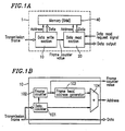
- Figure 1A is a block diagram illustrating a deinterleaving device 1 of Example 1 according to the present invention.
- Figure 1B is a block diagram illustrating an internal construction of a data write section 10 of the deinterleaving device 1 of Figure 1A
- Figure 1C is a block diagram illustrating an internal construction of a data read section 20 of the deinterleaving device 1 of Figure 1A.
- the deinterleaving device 1 includes the data write section 10, the data read section 20, and a memory 40 .
- the memory 40 is a 1M-word dual-port SRAM having a write port and a read port.
- Figure 2 illustrates an exemplified transmission frame to be processed by the device shown in Figure 1A.
- a transmission frame having 57,600 data is divided into 75 data segments each composed of 768 data.
- One data is assumed to be expressed by four bits, for example. It is also assumed that one data segment is transmitted via an OFDM symbol composed of 384 QPSK-modulated sub-carriers and is input to the deinterleaving device of this example after demodulation.
- inter-frame interleaving time interleaving
- inner-segment interleaving frequency interleaving
- inter-frame interleaving data are exchanged between a plurality of frames.
- a(-8,1) represents the first data in the minus eighth original frame.
- the order of data in each segment of an intermediate frame is changed.
- b(L,k) a(L-g ⁇ R(k,16) ⁇ , k) wherein R(m,r) denotes a remainder obtained when an integer m is divided by a natural number r, and g(n) denotes a function defined by expression (2) below.
- the function g(n) represents the rule of inter-frame interleaving.
- c(L,k) the relationship of expression (3) below is established between c(L,k) and b(L,k).
- Q(m,r) denotes a quotient obtained when an integer m is divided by a natural number r
- f(n) denotes a one-to-one function having a defined range and value range of integers of 0 to 767 inclusive.
- the function f(n) represents the rule of inner-segment interleaving. Detailed description on this function is not necessary in the understanding of the operation of the deinterleaving device.
- Figure 2 also illustrates detailed data in the zeroth original frame and the zeroth intermediate frame.
- Figure 3 illustrates detailed data of the zeroth to fifteenth intermediate frames, where data belonging to the zeroth original frame are hatched.
- the above transmission frame resembles a transmission frame in a method called European DAB Mode 2 .
- FIG. 4 illustrates a memory map of the memory 40 , where 17 compartments ( F0 to F16 ) for storing transmission frames are formed in the memory. Transmission frames are stored at a cycle of 17 frames in these compartments. In other words, once the zeroth to sixteenth frames are stored in compartments F0 to F16, the seventeenth frame is stored in compartment F0.
- the data write section 10 includes a data counter 101, a frame counter 102, a frame head address generator 103, and an adder 104.
- the data counter 101 is a 57,600-scale counter counting the number of data in transmission frames. When the count value reaches 57,599, the data counter 101 increments the count of the frame counter 102 by one.
- the frame counter 102 is a 17-scale counter.
- the frame head address generator 103 generates a value obtained by multiplying the value of the frame counter 102 by 57,600.
- the adder 104 sums the value of the data counter 101 and the output value of the frame head address generator 103 . Using the output of the adder 104 as an address, the transmission frames are cyclically stored in the compartments of the RAM.
- the data read section 20 includes a counter 201, a first operator 202, a frame head address generator 203, a second operator 204, a third operator 205, a ROM 206, and an adder 207.
- the counter 201 counts the number of data read requests m in response to a data read request signal received externally.
- the first operator 202 receives four less significant bits (n) of the counter 201 and outputs a function value g(n). The first operator 202 is only required to invert the bits of the input value as a nature of the function.
- a(L,p) c(L+g ⁇ R(p,16) ⁇ , 768 ⁇ Q(p,768)+h ⁇ R(p,768))) wherein the function h(n) is an inverse function of f(n).
- the frame head address generator 203 calculates expression (5) from the value Fc of the frame counter 102 and the output of the first operator 202, g ⁇ R(m,16) ⁇ , and outputs a value obtained by multiplying the value of expression (5) by 57600.
- the second operator 204 calculates the first term of expression (6).
- the third operator 205 calculates an argument R(m,768) of the function h of the second term of expression (6).
- the ROM 206 receives the value calculated by the third operator 205 as an address input, and outputs the function value h ⁇ R(m,768) ⁇ .
- the adder 207 sums the output values of the frame head address generator 203, the second operator 204, and the ROM 206. Using the output of the adder 207 as an address, the m-th data in the (L-16)th original frame is output in response to the m-th read request.
- the data write section and the data read section are constructed of respective exclusive circuits.
- the present invention is not restricted to this construction.
- a dual-port SRAM is used as the memory in this example.
- a one-port SRAM or DRAM may be used as the memory by additionally providing a control circuit which enables read and write operations by time division.
- OFDM is employed as the transmission method for transmission frames in this example, other transmission methods may be used.
- the structure of the transmission frame is not restricted to that described in this example.
- deinterleaving is performed during reading of data.
- deinterleaving may be performed during writing of data, and data may be written so that the data can be read from continuous addresses during reading.
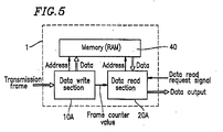
- Figure 5 illustrates an alternative deinterleaving device of this example which performs deinterleaving during writing.
- a data write section 10A Upon receipt of a transmission frame, a data write section 10A generates an address for each data in the transmission frame in the memory 40 corresponding to a relative position calculated from expression (5A) below in a compartment at a position of the memory 40 calculated from expression (6A) below, and stores the k-th data in the L-th transmission frame at the generated address. In this way, respective data in an original frame are arranged in the memory 40 .
- a data read section 20A can merely read the respective data in the original frame sequentially from the compartment Fc of the memory 40 .
- Figure 6 is a block diagram of a data read section 20B of a deinterleaving device of Example 2 according to the present invention.
- the construction of the deinterleaving device of this example is the same as that of the deinterleaving device of Example 1, except that the data read section 20 in Example 1 is replaced with the data read section 20B.
- the description of the data write section 10 and the memory 40 is therefore omitted here.
- Figure 7 illustrates an exemplified transmission frame to be processed by the deinterleaving device of this example.
- an intermediate frame having 57,600 data is divided into 900 data units each composed of 64 data.
- the intermediate frame has four multiplexed channels, and each channel occupies consecutive data units.
- the third channel occupies 140 data units from the 476th to the 615th data units.
- Inter-frame interleaving has been performed under the same rule as that described in Example 1 for each channel.
- the intermediate frame is divided into 75 data segments. Inner-segment interleaving is performed for each data segment to form the transmission frame. Data in the third channel is therefore included in 13 data segments from S39 to S51 as shown in Figure 7.
- the transmission frame with the above structure is stored in the memory 40 by the data write section 10 shown in Figure 1 in the procedure as described in Example 1.
- the data read section 20B in this example releases the interleaves provided in the transmission frame and the channel.
- the data read section 20B includes a counter 211, a register 212, and an operation portion 22.
- Components of the operation portion 22 which are the same as those in Example 1 are denoted by the same reference numerals and the description thereof is omitted here.
- the counter 211 upon receipt of a data read request signal, the counter 211 counts the number of read requests m .
- the number m circulates in the range of 0 to 8959 since the counter 211 counts data in the third channel cyclically.
- a shifter 213 shifts the output value Un of the register 212 by 6 bits leftward to obtain a value 64 times the value Un (i.e., 64Un).
- a second adder 214 sums the output values of the counter 211 and the shifter 213 (64Un + m). The resultant value is then input to the operators 202, 204, and 205, where the procedures described in Example 1 are performed. As a result, data in the third channel is output from the deinterleaving device (after deinterleaving).
- the deinterleaving device of this example includes a mechanism of selecting one of multiplexed channels in a transmission frame and deinterleaving data in the channel. For other channels which have not been selected, the circuit operation of the data read section 20B is inactivated to prevent data in such non-selected channels from being read and deinterleaved. This enables a significant reduction in power consumption compared with the deinterleaving device of Example 1.
- the data read section is constructed of an exclusive circuit.
- the present invention is not restricted to this construction.
- the memory and the transmission method for transmission frames are not restricted to those in this example.
- Figure 8 is a block diagram of a data read section 20C of a deinterleaving device of Example 3 according to the present invention.
- the construction of the deinterleaving device of this example is the same as that of the deinterleaving device of Example 1, except that the data read section 20 in Example 1 is replaced with the data read section 20C.
- the description of the data write section 10 and the memory 40 is therefore omitted here.
- Figure 9 illustrates an exemplified frame to be processed by the deinterleaving device of this example.
- the process of generating an intermediate frame from an original frame via inter-frame interleaving is the same as that shown in Figure 7 .
- the construction of channel multiplexing changes from a midway frame (the (n+15)th intermediate frame in Figure 9 ).
- the third channel which originally occupies the 476th to 615th data units, changes to occupy the 336th to 475th data units after the change of multiplexing construction.
- a new channel (the fifth channel) is added to the intermediate frame.
- the procedure of generating a transmission frame from the intermediate frame via inner-segment interleaving is the same as that described in Example 2. The description thereof is therefore omitted here.
- Inter-frame interleaving as shown in Figure 3 has been performed in the respective channels.
- two different channel start positions are temporarily generated for one channel. It is therefore required to calculate addresses of data in the memory 40 using the two different channel start positions. More specifically, for data which has been subjected to inter-frame interleaving before the change of multiplexing construction, the address of the data in the memory 40 must be calculated based on the old channel start position. For data which has been subjected to inter-frame interleaving after the change of multiplexing construction, the address of the data in the memory 40 must be calculated based on the new channel start position.
- the data read section 20C in this example includes a first counter 211 , a second counter 221 , two registers 223 , and an operation portion 24 .
- Components of the operation portion 24 which are the same as those in Example 1 are denoted by the same reference numerals and the description thereof is omitted here.
- the first counter 211 On receipt of a data read request signal, the first counter 211 counts the number of read requests m , as in the counter 211 shown in Figure 6 .
- the counter value m is associated with the m-th data in the selected channel.
- the second counter 221 On receipt of a channel multiplexing construction change signal, the second counter 221 initializes the count value to 15. The second counter 221 decrements the counter value for each transmission frame, and stops counting when the value reaches zero. In order to allow the second counter 221 to decrement the value for each transmission frame, the second counter 221 may receive an external signal which pulses at each boundary between transmission frames. The time period from the initialization and operation start until the operation stop of the second counter 221 corresponds to the time period from the generation of two different channel start positions until the settling to one channel start position.
- the two registers 223 constitute shift registers which store the new and old channel start positions. When a channel multiplexing construction change signal is input, these shift registers store the new channel start position and shift the old channel start position to the next stage, resulting in renewing both the new and old channel start positions.
- the value m of the first counter 211 and a value C of the second counter 221 are input to a comparator 222, and the output of the comparator 222 controls a selector 224 .
- the selector 224 selects the new channel start position if expression (7) below is satisfied, or selects the old channel start position if not satisfied, and supplies the result to a shifter 213.
- the subsequent procedure of the data read section 20C is the same as that in Example 2.
- the second counter value C obtained immediately after the receipt of a channel multiplexing construction change signal is 15.
- the value m is a value with which the right side of expression (7) becomes 15
- the m-th data belongs to the latest frame. Therefore, the new channel start position is adopted for the m-th data, while the old channel start position is adopted for data belonging to the other non-latest 15 frames.
- the new channel start position is adopted in the case where the right side of expression (7) is 14 or 15, i.e., for data belonging to the latest frame or the second latest frame.
- the old channel start position is adopted for data belonging to the remaining 14 frames. In this way, the number of data for which the new channel start position is adopted increases as the procedure moves to the next frame.
- the second counter value C reaches zero, the new channel start position is adopted for all data.
- the deinterleaving device of this example is capable of continuing deinterleaving even when the channel multiplexing construction changes midway through the process.
- the transmitter side can perform dynamic channel multiplexing.
- the data read section is constructed of an exclusive circuit in this example, the present invention is not restricted to this construction. Also, the memory and the transmission method for transmission frames are not restricted to those in this example.
- Figure 10 illustrates an exemplified transmission frame to be processed by a deinterleaving device of Example 4 according to the present invention.
- the number of data in the transmission frame, the number of data segments in the transmission frame, and the method of inner-segment interleaving are the same as those in Example 1.
- inter-frame interleaving is not performed for data belonging to the zeroth to 24th data segments of the transmission frame, while inter-frame interleaving is performed for data belonging to the 25th to 74th data segments as in Example 1.
- time interleaving is not performed for some OFDM symbols known as fast information channel, in order to avoid a delay due to time interleaving to realize prompt data transmission.
- more intensified error correction is performed by reducing the coding rate because data without time interleaving is vulnerable to time-axis burst error.
- Figure 11 illustrates a memory map of the memory 40 in Example 4.
- data segments which have not been subjected to inter-frame interleaving are stored in compartments E0 and E1
- data segments which have been subjected to inter-frame interleaving are stored in compartments F0 to F16.
- the compartments F0 to F16 correspond to the respective frames, and a total of 50 data segments from the 25th to 74th data segments are stored in respective compartments.
- addresses 0 to 652799 are allocated for the compartments F0 to F16.
- addresses 652800 to 671999 and 672000 to 691199 are allocated.
- Figure 11 is shown so that data is written in the compartment E0 and data is read from the compartment E1 , the read and write compartments are switched with each other every frame so as to avoid collision between the write and read operations.
- inter-frame interleaving has not been performed, it is not necessary to store data in the past 16 frames as in the case where inter-frame interleaving has been performed.
- the memory capacity can be saved.
- Example 4 For example, while a memory capacity of 979,200 words is required in Example 1, a memory capacity of only 691,200 words is required in Example 4. This reduction in memory capacity will contribute to a reduction in production cost of an LSI in the future when the LSI process technology advances to allow a large-capacity memory such as an inter-frame interleaving memory to be mounted in a signal processing LSI.
- Figure 12 is a block diagram of the deinterleaving device of Example 4 .
- a data read section 10D upon receipt of transmission frames, a data read section 10D generates addresses for the write port of the memory 40 , and sequentially writes data belonging to the 25th to 74th data segments of the transmission frames into 0 to 652799 addresses in the memory 40.
- the data write section 10D also writes data belonging to the zeroth to 24th data segments of the transmission frames into 652800 to 671999 addresses and 672000 to 691199 addresses in the memory 40 alternately.
- the data read section 20D reads data from 0 to 652799 addresses in the memory 40 while releasing both the time and frequency interleaves as in the data read section 20 shown in Figure 1.
- the data read section 20D also reads data from 652800 to 671999 addresses and 672000 to 691199 addresses in the memory 40 alternately.
- circuit construction and the memory are not restricted to those described in this example.
- FIG 13 is a block diagram of a deinterleaving device 3 of Example 5 according to the present invention.
- the deinterleaving device 3 of Example 5 is the same as the deinterleaving device 1 shown in Figure 1A, except that a memory (DRAM) 41 and a DRAM controller 30 are provided in place of the memory (SRAM) 40.
- DRAM memory
- SRAM memory
- the DRAM controller 30 temporarily holds an address and data from the data write section 10 and an address from the data read section 20, and outputs these addresses and data to the DRAM 41 at a predetermined timing.
- the DRAM controller 30 also temporarily holds data output from the DRAM 41 and outputs the data to the data read section 20 at a predetermined timing.
- these predetermined timings will be described in detail.
- Figure 14 is a timing chart of signals transmitted between the DRAM controller 30 and the DRAM 41.
- the DRAM controller 30 operates synchronously with a 25 MHz master clock and executes data write operation (six clocks) and data read operation (18 clocks) alternately in a cycle of 24 clocks. Since data is sequentially written into continuous addresses as described in Example 1, four data can be written during six clocks using a fast page mode.
- As for the read operation since a random read is performed, a cycle time of 110 ns or more is required as discussed in the description of the related art. In Example 5, one data is read during three clocks (120 ns).
- the timing of various signals shown in Figure 14 satisfies the timing restriction for a standard DRAM having an access time of 60 ns.
- the deinterleaving device of this example executes four-data write and six-data read during 24 clocks. Accordingly, the average input data rate is 4.167 MHz and the average output data rate is 6.25 MHz. It is therefore sufficiently possible to obtain an output data rate of 1.536 MHz after error correction even for the European DAB standards mentioned in the description of the related art.
- the deinterleaving device of this example in which data is written using the fast page mode, realizes a high input/output data rates while using a DRAM with a low unit cost per bit.
- circuit construction and the transmission method for transmission frames are not restricted to those described in this example.
- FIG 15 is a block diagram of a deinterleaving device 3 of Example 6 according to the present invention.
- the inner construction of the deinterleaving device 3 is the same as that shown in Figure 13.
- an OFDM demodulator 2 is provided upstream of the deinterleaving device 3.
- the transmission frame to be processed is composed of 57,600 data and divided into 75 data segments. Each data segment is transmitted via an OFDM symbol composed of 384 QPSK-modulated sub-carriers.
- the transmission frame is input to the deinterleaving device 3 after being demodulated by the OFDM demodulator 2.
- Figure 16 illustrates part of the transmission frame to be processed by the deinterleaving device of this example.
- the length of each OFDM symbol is 250 ⁇ s, and a guard interval with a length of a quarter of the symbol length (62.5 ⁇ s) is added to each OFDM symbol.
- the guard interval is provided to prevent inter-symbol interference at multi-path signal receiving.
- the rear quarter portion of each symbol is copied at the head of the symbol as the guard interval. Since it takes time to retrieve and demodulate data, the OFDM demodulator 2 outputs the demodulation result delaying two symbols from the input. During the guard interval, the input transmission frame is discarded, the internal operation is stopped, and the demodulation result is not output.
- the memory map of the memory (DRAM) 41 of the deinterleaving device of this example is the same as that shown in Figure 4. In this case, it is after 16 frames, i.e., after 375 ms, at maximum that written data is read. After this time period, the data will be volatilized unless the DRAM is refreshed.
- the interval releasing device of this example performs a refresh operation during the guard interval at a timing shown in Figure 17. In other words, since no data is written during the guard interval, refresh operation is performed in place of write operation. This allows the refresh operation of the DRAM to be performed without reducing the input/output data rates nor changing the input/output timings.
- the refresh operation since six clocks (240 ns) are used for one refresh operation, about 260 refresh operations (62.5 ⁇ s/240 ns) per symbol can be performed.
- the 1,024 refresh operations required for refreshing the entire DRAM 41 are completed within four symbols, i.e., within a time period of 1.25 ms. Since the time period of about 16 ms is enough for a current standard DRAM, the refresh operation may be performed at a lower speed than that in this example.
- circuit construction and the transmission method for transmission frames are not restricted to those described in this example.
- the deinterleaving device does not require a memory for frequency interleave nor an output buffer. This allows for a less expensive device compared with the conventional devices.
- a mechanism of selecting one of multiplexed channels in a transmission frame to deinterleave only data of the selected channel is provided. This serves to greatly reduce power consumption of the circuit.
- Deinterleaving operations can be continuously performed even when the channel multiplexing construction changes midway. This allows for dynamic channel multiplexing on the transmitter side.
- the storage positions of data are separated depending on the existence of inter-frame interleaving. This allows for saving of the capacity of the time interleave memory and thus reduction in LSI production cost.
- Data is written using the fast page mode. This realizes high input/output data rates while using a DRAM with a low unit cost per bit.
- Refresh operation is performed during the guard interval, allowing for effective DRAM refreshing.
Description
- The present invention relates to a device for deinterleaving interleaved digital transmission data, and more particularly, to a deinterleaving device which releases a plurality of types of interleaving simultaneously.
- In recent years, digitalization in broadcasting technology has been in rapid progress. For example, terrestrial digital audio broadcasting employing a transmission method called orthogonal frequency division multiplex (OFDM) has been realized. In such a broadcasting method, in general, (1) an audio signal is coded after an error correction code is added thereto, (2) the coded data is divided into blocks (normally called "frames") of a predetermined length, and (3) each frame is constructed of a plurality of OFDM symbols. In addition to the above, processing steps of (4) rearranging data between frames (time interleave) and (5) changing the order of sub-carriers in a symbol (frequency interleave) may be performed. By combining the two types of interleave (4) and (5) with error correction, the audio signal can be substantially restored to its original state even if continuous data on a time axis and a frequency axis are partially missing.
- If such radio wave is reflected from a tall building, a mountain, and the like during reception of broadcasting, the frequency characteristic of a transmission path is no longer flat, causing a degradation of a received signal, called multi-path interference, in some cases. In such cases, the receiving power of continuous sub-carriers on a frequency axis drops simultaneously (frequency selective phasing). Therefore, if frequency interleaving is not performed, data error tends to occur in bursts, and thus the effect of an error correction code is unlikely to be obtained. Also, in the case of reception of broadcasting in a moving car and the like, impulse-like noise from an ignition plug of an engine and the like and instantaneous reduction of the electric field intensity may possibly occur. In order to avoid influences from such occurrences, interleave on a time axis is also required.
- For the above reasons, time and frequency interleaves are indispensable for digital broadcasting employing the OFDM method. Receivers of such broadcasting are therefore required to include a function of deinterleaving. For example, Japanese Laid-Open Publication No. 8-316933 and Japanese National Phase PCT Laid-Open Publication No. 9-509818 and No. 9-509819 disclose a same construction of a receiver for digital audio broadcasting (hereinbelow, abbreviated as DAB) which has a function of releasing time and frequency interleaves.
- In EP-A-0 740 437 (see Figure 2 of this publication), for example, frequency interleave is released when an output of a demodulator DEM is written in a demodulator output buffer DOB. The resultant data is temporarily written in a first section of a time deinterleave memory TDM(1). The frequency-deinterleaved data is then returned to the demodulator output buffer DOB and written this time in a second section of the time deinterleave memory TDM(2). During this writing of data in TDM(2), time interleave is released. The resultant data released from both time and frequency interleaves is then transferred to a deinterleaver output buffer (IOB) and then input to a Viterbi decoder DEC for error correction.
- In general, delay occurs when serial data is interleaved. In order to deinterleave, it is necessary to provide a memory device for temporarily storing standby data during the delay time. Such a memory device is generally a semiconductor memory such as a DRAM, an SRAM, and a register. In the above exemplified receiver for DAB, the demodulator output buffer DOB for releasing frequency interleave and the first section of the time deinterleave memory TDM(1) for releasing time interleave correspond to the memory device for temporarily storing data described above. The interleave-specific delay of time interleave is enormously larger than that of frequency interleave. Accordingly, while the memory capacity of DOB is 12 kbits, that of TDM is as large as 1,024 kbits (1 kbit = 1,024 bits). In this case, it should be noted that the memory capacity of the time deinterleave memory TDM is limited on the assumption that only part of a plurality of multiplexed services in a DAB signal is demodulated.
- If the output data rate (output speed) after deinterleaving is not matched with the input data rate of an error corrector, a storage device called a buffer (normally, a memory) is required to achieve matching of these rates. Some error correctors read data intermittently depending on the error correction coding method. In general, therefore, the above two data rates are not matched with each other. In the above exemplified receiver for DAB, the second section of the time deinterleave memory TDM(2) and the deinterleaver output buffer IOB serve to match the data rates.
- The above conventional device requires high-speed and complicated processing, which is not easily realized by a general purpose processor. Such processing is normally performed by an exclusive signal processing LSI (large scale integrated circuit). As of today, however, it is not preferable economically to mount a large-capacity memory such as the time deinterleave memory in a signal processing LSI. Therefore, the conventional deinterleaving device as described above has a construction that a general external large-capacity memory is added to an exclusive signal processing LSI.
- The above conventional receiver for DAB has the following problems. Since frequency and time interleaves are separately released, respective memories for releasing these interleaves are required. If a memory for frequency interleave and an output buffer are incorporated in a signal processing LSI, production cost of the LSI increases since memories normally occupy a large area on a chip. In the case where such memory and buffer are not incorporated in the LSI, external memories are separately required, resulting in increasing the cost of the receiver.
- In reality, it is possible to release both time and frequency interleaves using a single external memory. For example, data may be written in a memory so that the data is arranged in a state that frequency interleave has been released, and time interleave may be released when the data is read. In this construction, however, access to random addresses is performed in the memory during both write and read operations. In such random access, if the input/output data rates are high, a DRAM having long random read/random write times fails to catch up with the processing speed.
- Hereinbelow, the processing speed will be described, taking as an example a receiver of a DAB signal used in broadcasting in Europe. In European DAB standards, the coding rate to an original code is 1/4 at minimum. In order to obtain an output data rate of 1.536 Mbps after error correction, an output data rate of four times the above data rate, i.e., 4.096 MHz, is required after deinterleaving. The input data rate is 4.096 MHz, and the average of the input/output data rates is 5.12 MHz.
- The random read or random write cycle time is 110 ns for a standard DRAM having an access time of 60 ns. Therefore, since 220 ns is required for one random read/random write, it is not possible to obtain an average input/output data rate equal to or more than 4.545 MHz (= 1/220 ns). In order to obtain the output data rate of 6.144 MHz, it is necessary to temporarily store data in a buffer (i.e., a large-capacity memory) before being output or to use an SRAM and the like capable of realizing high-speed random access, in place of the DRAM. However, using a buffer increases production cost of the LSI, and an SRAM has a high cost per bit compared with a DRAM.
- The deinterleaving device of this invention deinterleaves an input transmission frame and outputs the deinterleaved frame, the transmission frame being obtained by performing inter-frame interleaving for an original frame to form an intermediate frame and performing inner-segment interleaving for at least one data segment included in the intermediate frame. The deinterleaving device includes: a memory; a data write section for receiving the transmission frame and writing the transmission frame into the memory; and a data read section for releasing the inter-frame interleaving and the inner-segment interleaving simultaneously when reading data from the memory and outputting the data.
- In one embodiment of the invention, the data write section receives data in a plurality of transmission frames and writes the data into the memory, and the data read section determines the order of the data in each of the transmission frames in a state where the inter-frame interleaving and the inner-segment interleaving are released by calculating backward a rearranging rule of the inner-segment interleaving and a rearranging rule of the inter-frame interleaving, reads the data from the memory in the determined order, and outputs the data.
- In another embodiment of the invention, the data write section includes: a data counter for counting the number of data in a transmission frame; a frame counter for counting the number of transmission frames; a first frame head address generator for generating an address in the memory at which head data of the transmission frame is to be stored based on a value of the frame counter; and a first adder for summing a value of the data counter and an output value of the first frame head address generator and outputting the result as an address in the memory.
- In still another embodiment of the invention, the data read section includes: a counter for counting the number of data read requests; a second frame head address generator for generating an address in the memory at which the head data of the transmission frame is stored based on a value of the counter and a value of the frame counter of the data write section; a ROM for storing a rearranging rule of the inner-segment interleaving; a first operator for calculating a data segment to which desired output data belongs; a second operator for calculating a relative position of the desired output data in the data segment using the ROM; and a second adder for summing output values of the second frame head address generator, the first operator, and the second operator and outputting the result as an address in the memory.
- In still another embodiment of the invention, the transmission frame includes, at a stage of the intermediate frame, a data segment for which the inter-frame interleaving has been performed and a data segment for which the inter-frame interleaving has not been performed, the data write section writes the data segment for which the inter-frame interleaving has been performed and the data segment for which the inter-frame interleaving has not been performed at different storage positions of the memory, and the data read section releases the inter-frame interleaving and the inner-segment interleaving simultaneously for the data segment for which the inter-frame interleaving has been performed when reading data from the memory and outputs the data, while the data read section releases the inner-segment interleaving for the data segment for which the inter-frame interleaving has not been performed when reading data from the memory and outputs the data.
- In still another embodiment of the invention, the data segments are transmitted via sub-carriers included in at least one symbol constituting orthogonal frequency division multiplex, and the transmission frame includes a plurality of symbols constituting orthogonal frequency division multiplex.
- In still another embodiment of the invention, the memory is a DRAM having a fast page mode, and the data write section writes at least two consecutive data in the transmission frame into continuous addresses in the DRAM in the fast page mode.
- In still another embodiment of the invention, the data segment is transmitted via sub-carriers included in at least one symbol constituting orthogonal frequency division multiplex, a guard interval is added to the symbol constituting orthogonal frequency division multiplex, the transmission frame includes a plurality of symbols constituting orthogonal frequency division multiplex, an orthogonal frequency division multiplex demodulator is connected upstream of the deinterleaving device, and refresh operation of the DRAM is performed during the guard interval.
- Alternatively, the deinterleaving device of this invention deinterleaves an input transmission frame and outputs the deinterleaved frame, the transmission frame being obtained by performing inter-frame interleaving for an original frame to form an intermediate frame and performing inner-segment interleaving for at least one data segment included in the intermediate frame. The deinterleaving device includes: a memory; a data write section for releasing the inter-frame interleaving and the inner-segment interleaving simultaneously when writing data in the memory; and a data read section for reading data from the memory and outputting the data.
- In one embodiment of the invention, the data write section receives data in a plurality of transmission frames, determines the order of the data in each of the transmission frames in a state where the inter-frame interleaving and the inner-segment interleaving are released by calculating backward a rearranging rule of the inner-segment interleaving and a rearranging rule of the inter-frame interleaving, and writes the data in the memory in the determined order.
- In another embodiment of the invention, the data segments are transmitted via sub-carriers included in at least one symbol constituting orthogonal frequency division multiplex, and the transmission frame includes a plurality of symbols constituting orthogonal frequency division multiplex.
- In still another embodiment of the invention, the memory is a DRAM having a fast page mode, and the data write section writes at least two consecutive data in the transmission frame at continuous addresses in the DRAM in the fast page mode.
- In still another embodiment of the invention, the data segment is transmitted via sub-carriers included in at least one symbol constituting orthogonal frequency division multiplex, a guard interval is added to the symbol constituting orthogonal frequency division multiplex, the transmission frame includes a plurality of symbols constituting orthogonal frequency division multiplex, an orthogonal frequency division multiplex demodulator is connected upstream of the deinterleaving device, and refresh operation of the DRAM is performed during the guard interval.
- Alternatively, the deinterleaving device of this invention deinterleaves an input transmission frame and outputs the deinterleaved frame, the transmission frame being obtained by performing inter-frame interleaving for an original frame including at least one channel to form an intermediate frame multiplexed by allocating the channel at a predetermined channel start position and performing inner-segment interleaving for at least one data segment included in the intermediate frame. The deinterleaving device includes: a memory; a data write section for writing the transmission frame into the memory; and a data read section for releasing the inter-frame interleaving and the inner-segment interleaving for data in the channel simultaneously by referring to the channel start position of the channel when the channel start position is designated during reading of data from the memory, and outputting the data of the channel.
- In one embodiment of the invention, the data write section receives data in a plurality of transmission frames and stores the data in the memory, and the data read section determines the order of the data in each of the transmission frames in a state where the inter-frame interleaving and the inner-segment interleaving are released by calculating backward a rearranging rule of the inner-segment interleaving and a rearranging rule of the inter-frame interleaving, reads the data in the memory in the determined order, and outputs the data.
- In another embodiment of the invention, the data read section calculates a storage position of data in the memory based on the channel start position and the number of data read requests when the channel start position is designated during reading of data from the memory.
- In still another embodiment of the invention, the data read section includes: a register for storing the channel start position; a counter for counting the number of data read requests; and an operator for calculating the storage position of data in the memory based on values of the register and the counter.
- In still another embodiment of the invention, during reading of data from the memory, when the data read section receives a channel multiplexing construction change signal indicating a change of a channel multiplexing construction of the original frame, the data read section releases the inter-frame interleaving and the inner-segment interleaving for data in the channel simultaneously by referring to an old channel start position before the receipt of the channel multiplexing construction change signal and a new channel start position after the receipt of the channel multiplexing construction change signal, and outputs the data of the channel.
- In still another embodiment of the invention, when the data read section receives the channel multiplexing construction change signal, the data read section selects one of the old channel start position and the new channel start position based on the old and new channel start positions, the number of data read requests, and the number of transmission frames, and calculates the storage position of the data in the memory.
- In still another embodiment of the invention, the data read section includes: a register for storing the old and new channel start positions and renewing the old and new channel start positions in response to the channel multiplexing construction change signal; a first counter for counting the number of data read requests; a second counter for counting the number of transmission frames, the second counter being initialized on receipt of the channel multiplexing construction change signal; and an operator for calculating a storage position of data in the memory based on values of the register, the first counter, and the second counter.
- In still another embodiment of the invention, the transmission frame includes, at a stage of the intermediate frame, a data segment for which the inter-frame interleaving has been performed and a data segment for which the inter-frame interleaving has not been performed, the data write section writes the data segment for which the inter-frame interleaving has been performed and the data segment for which the inter-frame interleaving has not been performed into different storage positions of the memory, and the data read section releases the inter-frame interleaving and the inner-segment interleaving simultaneously for the data segment for which the inter-frame interleaving has been performed when reading data from the memory and outputs the data, while the data read section releases the inner-segment interleaving for the data segment for which the inter-frame interleaving has not been performed when reading data from the memory and outputs the data.
- In still another embodiment of the invention, the data segments are transmitted via sub-carriers included in at least one symbol constituting orthogonal frequency division multiplex, and the transmission frame includes a plurality of symbols constituting orthogonal frequency division multiplex.
- In still another embodiment of the invention, the memory is a DRAM having a fast page mode, and the data write section writes at least two consecutive data in the transmission frame at continuous addresses in the DRAM in the fast page mode.
- In still another embodiment of the invention, the data segment is transmitted via sub-carriers included in at least one symbol constituting orthogonal frequency division multiplex, a guard interval is added to the symbol constituting orthogonal frequency division multiplex, the transmission frame includes a plurality of symbols constituting orthogonal frequency division multiplex, an orthogonal frequency division multiplex demodulator is connected upstream of the deinterleaving device, and refresh operation of the DRAM is performed during the guard interval.
- Thus, the invention described herein makes possible the advantages of (1) providing a less expensive deinterleaving device which does not require a frequency interleave memory nor an output buffer, and (2) providing a deinterleaving device capable of realizing a high output data rate using an inexpensive DRAM as an external memory.
- These and other advantages of the present invention will become apparent to those skilled in the art upon reading and understanding the following detailed description with reference to the accompanying figures.
-
- Figure 1A is a block diagram illustrating a deinterleaving device of Example 1 according to the present invention;
- Figure 1B is a block diagram of a data write section of the deinterleaving device of Example 1;
- Figure 1C is a block diagram of a data read section of the deinterleaving device of Example 1;
- Figure 2 illustrates an example of frame to be processed by the deinterleaving device of Example 1;
- Figure 3 illustrates details of an intermediate frame shown in Figure 2;
- Figure 4 illustrates a memory map of a memory of the deinterleaving device of Example 1;
- Figure 5 is a block diagram illustrating another deinterleaving device of Example 1 according to the present invention;
- Figure 6 is a block diagram of a data write section of a deinterleaving device of Example 2 according to the present invention;
- Figure 7 illustrates an example of frame to be processed by the deinterleaving device of Example 2;
- Figure 8 is a block diagram of a data write section of a deinterleaving device of Example 3 according to the present invention;
- Figure 9 illustrates an example of frame to be processed by the deinterleaving device of Example 3;
- Figure 10 illustrates an example of a transmission frame to be processed by a deinterleaving device of Example 4 according to the present invention;
- Figure 11 illustrates a memory map of a RAM of the deinterleaving device of Example 4;
- Figure 12 is a block diagram illustrating the deinterleaving device of Example 4;
- Figure 13 is a block diagram illustrating a deinterleaving device of Example 5 according to the present invention;
- Figure 14 is a timing chart of signals transmitted and received between a DRAM controller and a DRAM of the deinterleaving device of Example 5 shown in Figure 13;
- Figure 15 is a block diagram illustrating a deinterleaving device of Example 6 according to the present invention;
- Figure 16 illustrates part of a transmission frame to be processed by the deinterleaving device of Example 6; and
- Figure 17 is a timing chart of signals transmitted and received between a DRAM controller and a DRAM during a guard interval.
-
- Hereinbelow, the present invention will be described by way of examples with reference to the relevant drawings.
- Figure 1A is a block diagram illustrating a
deinterleaving device 1 of Example 1 according to the present invention. Figure 1B is a block diagram illustrating an internal construction of adata write section 10 of thedeinterleaving device 1 of Figure 1A, and Figure 1C is a block diagram illustrating an internal construction of a data readsection 20 of thedeinterleaving device 1 of Figure 1A. - Referring to Figure 1A, the
deinterleaving device 1 includes the data writesection 10, the data readsection 20, and amemory 40. Thememory 40 is a 1M-word dual-port SRAM having a write port and a read port. - Figure 2 illustrates an exemplified transmission frame to be processed by the device shown in Figure 1A. Referring to Figure 2, a transmission frame having 57,600 data is divided into 75 data segments each composed of 768 data. One data is assumed to be expressed by four bits, for example. It is also assumed that one data segment is transmitted via an OFDM symbol composed of 384 QPSK-modulated sub-carriers and is input to the deinterleaving device of this example after demodulation.
- As is shown in Figure 2, the transmission frame (after demodulation) has been subjected to inter-frame interleaving (time interleaving) and inner-segment interleaving (frequency interleaving), which correspond to interleave on a time axis and interleave on a frequency axis, respectively.
- In the inter-frame interleaving, data are exchanged between a plurality of frames. For example, in the zeroth intermediate frame, a(-8,1) represents the first data in the minus eighth original frame.
- In the inner-segment interleaving, the order of data in each segment of an intermediate frame is changed.
- The rule of the above interleaves will be described in detail.
- Assuming that the k-th data in.the L-th original frame is represented by a(L,k), and the k-th data in the L-th intermediate frame after inter-frame interleaving is represented by b(L,k), the two data have the relationship of expression (1) below.
- Further, assuming that the k-th data in the L-th transmission frame after inner-segment interleaving is represented by c(L,k), the relationship of expression (3) below is established between c(L,k) and b(L,k).
- Figure 2 also illustrates detailed data in the zeroth original frame and the zeroth intermediate frame. Figure 3 illustrates detailed data of the zeroth to fifteenth intermediate frames, where data belonging to the zeroth original frame are hatched. The above transmission frame resembles a transmission frame in a method called
European DAB Mode 2. - When a transmission frame is input to the
deinterleaving device 1, the data writesection 10 generates addresses for the write port of thememory 40, and sequentially writes data in the transmission frame into continuous addresses in thememory 40. Figure 4 illustrates a memory map of thememory 40, where 17 compartments (F0 to F16) for storing transmission frames are formed in the memory. Transmission frames are stored at a cycle of 17 frames in these compartments. In other words, once the zeroth to sixteenth frames are stored in compartments F0 to F16, the seventeenth frame is stored in compartment F0. - Referring to Figure 1B, for realizing the above function, the data write
section 10 includes a data counter 101, aframe counter 102, a framehead address generator 103, and anadder 104. The data counter 101 is a 57,600-scale counter counting the number of data in transmission frames. When the count value reaches 57,599, the data counter 101 increments the count of theframe counter 102 by one. Theframe counter 102 is a 17-scale counter. The framehead address generator 103 generates a value obtained by multiplying the value of theframe counter 102 by 57,600. Theadder 104 sums the value of the data counter 101 and the output value of the framehead address generator 103. Using the output of theadder 104 as an address, the transmission frames are cyclically stored in the compartments of the RAM. - Referring to Figure 4, when a transmission frame is being written in the compartment F0, data is read from the compartments F1 to F16. At this time, the latest frame is stored in the compartment F16 and the oldest frame is stored in the compartment F1. When a next transmission frame is written in the compartment F1, data is read from the compartments F2 to F16 and F0. At this time, the latest frame is stored in the compartment F0 and the oldest frame is stored in the compartment F2. In this way, the compartment from which data is read is cycled for each frame, so that the read and write operations will not collide with each other.
- Referring to Figure 1C, for realizing the above function, the data read
section 20 includes acounter 201, afirst operator 202, a framehead address generator 203, asecond operator 204, athird operator 205, aROM 206, and anadder 207. Thecounter 201 counts the number of data read requests m in response to a data read request signal received externally. Thefirst operator 202 receives four less significant bits (n) of thecounter 201 and outputs a function value g(n). Thefirst operator 202 is only required to invert the bits of the input value as a nature of the function. - Herein, by calculating backward from the definitions of the k-th data in the L-th original frame a(L,k), the k-th data in the L-th intermediate frame b(L,k) represented by expression (1), and the k-th data in the L-th transmission frame c(L,k) represented by expression (3), as described above, the relationship of expression (4) below is established.
- Assuming that the L-th transmission frame is currently being written in the compartment Fc (i.e., the value of the
frame counter 102 is Fc), it is possible to read the (L-16)th original frame from a compartment other than the compartment Fc. From the above-described data write method and expression (4), it is found that the m-th data in the (L-16)th original frame is stored in a compartment at a position calculated from expression (5) below and that the relative position in the compartment is calculated from expression (6) below. The resultant data is an output for the m-th read request. - The frame
head address generator 203 calculates expression (5) from the value Fc of theframe counter 102 and the output of thefirst operator 202, g{R(m,16)}, and outputs a value obtained by multiplying the value of expression (5) by 57600. Thesecond operator 204 calculates the first term of expression (6). Thethird operator 205 calculates an argument R(m,768) of the function h of the second term of expression (6). TheROM 206 receives the value calculated by thethird operator 205 as an address input, and outputs the function value h{R(m,768)}. Theadder 207 sums the output values of the framehead address generator 203, thesecond operator 204, and theROM 206. Using the output of theadder 207 as an address, the m-th data in the (L-16)th original frame is output in response to the m-th read request. - As described above, in the deinterleaving device of this example, since time interleave and frequency interleave are released simultaneously during reading data from the memory, a memory for frequency interleave is no more required. Moreover, since data is output in response to a data read request signal, an output buffer is no more required. With these effects, the capacity of the memory (SRAM) can be made small compared with the conventional examples, and thus a less expensive device is realized.
- In this example, the data write section and the data read section are constructed of respective exclusive circuits. The present invention is not restricted to this construction. For example, it is possible, in principle, to use a general purpose processor to realize substantially the same function as that described above. A dual-port SRAM is used as the memory in this example. Alternatively, a one-port SRAM or DRAM, for example, may be used as the memory by additionally providing a control circuit which enables read and write operations by time division. Although, OFDM is employed as the transmission method for transmission frames in this example, other transmission methods may be used. Also, the structure of the transmission frame is not restricted to that described in this example.
- In this example, deinterleaving is performed during reading of data. Alternatively, deinterleaving may be performed during writing of data, and data may be written so that the data can be read from continuous addresses during reading. By this construction, also, substantially the same effect as that described above can be obtained.
- For example, Figure 5 illustrates an alternative deinterleaving device of this example which performs deinterleaving during writing. Upon receipt of a transmission frame, a
data write section 10A generates an address for each data in the transmission frame in thememory 40 corresponding to a relative position calculated from expression (5A) below in a compartment at a position of thememory 40 calculated from expression (6A) below, and stores the k-th data in the L-th transmission frame at the generated address. In this way, respective data in an original frame are arranged in thememory 40. A data read section 20A can merely read the respective data in the original frame sequentially from the compartment Fc of thememory 40. - Figure 6 is a block diagram of a data read
section 20B of a deinterleaving device of Example 2 according to the present invention. The construction of the deinterleaving device of this example is the same as that of the deinterleaving device of Example 1, except that the data readsection 20 in Example 1 is replaced with the data readsection 20B. The description of the data writesection 10 and thememory 40 is therefore omitted here. - Figure 7 illustrates an exemplified transmission frame to be processed by the deinterleaving device of this example. Referring to Figure 7, an intermediate frame having 57,600 data is divided into 900 data units each composed of 64 data. The intermediate frame has four multiplexed channels, and each channel occupies consecutive data units. For example, the third channel occupies 140 data units from the 476th to the 615th data units. Inter-frame interleaving has been performed under the same rule as that described in Example 1 for each channel. As in Example 1, the intermediate frame is divided into 75 data segments. Inner-segment interleaving is performed for each data segment to form the transmission frame. Data in the third channel is therefore included in 13 data segments from S39 to S51 as shown in Figure 7.
- The transmission frame with the above structure is stored in the
memory 40 by the data writesection 10 shown in Figure 1 in the procedure as described in Example 1. - Thereafter, the data read
section 20B in this example releases the interleaves provided in the transmission frame and the channel. Referring to Figure 6, the data readsection 20B includes acounter 211, aregister 212, and an operation portion 22. Components of the operation portion 22 which are the same as those in Example 1 are denoted by the same reference numerals and the description thereof is omitted here. - In the data read
section 20B, upon receipt of a data read request signal, thecounter 211 counts the number of read requests m. The number m circulates in the range of 0 to 8959 since thecounter 211 counts data in the third channel cyclically. - The
register 212 stores the channel start position designated externally. For example, in the case where the third channel of the above transmission frame is selected, the head data unit Number Un (= 476) is stored as the channel start position. - A
shifter 213 shifts the output value Un of theregister 212 by 6 bits leftward to obtain avalue 64 times the value Un (i.e., 64Un). Asecond adder 214 sums the output values of thecounter 211 and the shifter 213 (64Un + m). The resultant value is then input to theoperators - As described above, the deinterleaving device of this example includes a mechanism of selecting one of multiplexed channels in a transmission frame and deinterleaving data in the channel. For other channels which have not been selected, the circuit operation of the data read
section 20B is inactivated to prevent data in such non-selected channels from being read and deinterleaved. This enables a significant reduction in power consumption compared with the deinterleaving device of Example 1. - In this example, the data read section is constructed of an exclusive circuit. The present invention is not restricted to this construction. Also, the memory and the transmission method for transmission frames are not restricted to those in this example.
- Figure 8 is a block diagram of a data read
section 20C of a deinterleaving device of Example 3 according to the present invention. The construction of the deinterleaving device of this example is the same as that of the deinterleaving device of Example 1, except that the data readsection 20 in Example 1 is replaced with the data readsection 20C. The description of the data writesection 10 and thememory 40 is therefore omitted here. - Figure 9 illustrates an exemplified frame to be processed by the deinterleaving device of this example. Referring to Figure 9, the process of generating an intermediate frame from an original frame via inter-frame interleaving is the same as that shown in Figure 7. In this example, however, the construction of channel multiplexing changes from a midway frame (the (n+15)th intermediate frame in Figure 9). For example, in the illustrated example, the third channel, which originally occupies the 476th to 615th data units, changes to occupy the 336th to 475th data units after the change of multiplexing construction. Also, after the change of multiplexing construction, a new channel (the fifth channel) is added to the intermediate frame. The procedure of generating a transmission frame from the intermediate frame via inner-segment interleaving is the same as that described in Example 2. The description thereof is therefore omitted here.
- Inter-frame interleaving as shown in Figure 3 has been performed in the respective channels. In the case where the multiplexing construction is changed somewhere in the 16 frames to be deinterleaved, two different channel start positions are temporarily generated for one channel. It is therefore required to calculate addresses of data in the
memory 40 using the two different channel start positions. More specifically, for data which has been subjected to inter-frame interleaving before the change of multiplexing construction, the address of the data in thememory 40 must be calculated based on the old channel start position. For data which has been subjected to inter-frame interleaving after the change of multiplexing construction, the address of the data in thememory 40 must be calculated based on the new channel start position. - Referring to Figure 8, in order to deinterleave data in each channel, the data read
section 20C in this example includes afirst counter 211, asecond counter 221, tworegisters 223, and anoperation portion 24. Components of theoperation portion 24 which are the same as those in Example 1 are denoted by the same reference numerals and the description thereof is omitted here. - On receipt of a data read request signal, the
first counter 211 counts the number of read requests m, as in thecounter 211 shown in Figure 6. The counter value m is associated with the m-th data in the selected channel. - On receipt of a channel multiplexing construction change signal, the
second counter 221 initializes the count value to 15. Thesecond counter 221 decrements the counter value for each transmission frame, and stops counting when the value reaches zero. In order to allow thesecond counter 221 to decrement the value for each transmission frame, thesecond counter 221 may receive an external signal which pulses at each boundary between transmission frames. The time period from the initialization and operation start until the operation stop of thesecond counter 221 corresponds to the time period from the generation of two different channel start positions until the settling to one channel start position. - The two
registers 223 constitute shift registers which store the new and old channel start positions. When a channel multiplexing construction change signal is input, these shift registers store the new channel start position and shift the old channel start position to the next stage, resulting in renewing both the new and old channel start positions. - The value m of the
first counter 211 and a value C of thesecond counter 221 are input to acomparator 222, and the output of thecomparator 222 controls aselector 224. Theselector 224 selects the new channel start position if expression (7) below is satisfied, or selects the old channel start position if not satisfied, and supplies the result to ashifter 213. The subsequent procedure of the data readsection 20C is the same as that in Example 2. - The second counter value C obtained immediately after the receipt of a channel multiplexing construction change signal is 15. As is apparent from expression (4), when the value m is a value with which the right side of expression (7) becomes 15, the m-th data belongs to the latest frame. Therefore, the new channel start position is adopted for the m-th data, while the old channel start position is adopted for data belonging to the other non-latest 15 frames.
- When the procedure moves to the next frame, the value C becomes 14. In this case, the new channel start position is adopted in the case where the right side of expression (7) is 14 or 15, i.e., for data belonging to the latest frame or the second latest frame. The old channel start position is adopted for data belonging to the remaining 14 frames. In this way, the number of data for which the new channel start position is adopted increases as the procedure moves to the next frame. When the second counter value C reaches zero, the new channel start position is adopted for all data.
- With the above construction, the deinterleaving device of this example is capable of continuing deinterleaving even when the channel multiplexing construction changes midway through the process. Thus, if a receiver is provided with the deinterleaving device of this example, the transmitter side can perform dynamic channel multiplexing.
- Although the data read section is constructed of an exclusive circuit in this example, the present invention is not restricted to this construction. Also, the memory and the transmission method for transmission frames are not restricted to those in this example.
- Figure 10 illustrates an exemplified transmission frame to be processed by a deinterleaving device of Example 4 according to the present invention. Referring to Figure 10, the number of data in the transmission frame, the number of data segments in the transmission frame, and the method of inner-segment interleaving are the same as those in Example 1. In the transmission frame shown in Figure 10, however, inter-frame interleaving is not performed for data belonging to the zeroth to 24th data segments of the transmission frame, while inter-frame interleaving is performed for data belonging to the 25th to 74th data segments as in Example 1.
- In reality, in European DAB transmission frames, time interleaving is not performed for some OFDM symbols known as fast information channel, in order to avoid a delay due to time interleaving to realize prompt data transmission. In this case, more intensified error correction is performed by reducing the coding rate because data without time interleaving is vulnerable to time-axis burst error.
- Figure 11 illustrates a memory map of the
memory 40 in Example 4. Unlike Example 1, data segments which have not been subjected to inter-frame interleaving are stored in compartments E0 and E1, while data segments which have been subjected to inter-frame interleaving are stored in compartments F0 to F16. The compartments F0 to F16 correspond to the respective frames, and a total of 50 data segments from the 25th to 74th data segments are stored in respective compartments. Thus, addresses 0 to 652799 are allocated for the compartments F0 to F16. For the compartments E0 and E1, in which data in the first 25 data segments in the respective transmission frame are alternately stored, addresses 652800 to 671999 and 672000 to 691199 are allocated. - Although Figure 11 is shown so that data is written in the compartment E0 and data is read from the compartment E1, the read and write compartments are switched with each other every frame so as to avoid collision between the write and read operations.
- If inter-frame interleaving has not been performed, it is not necessary to store data in the past 16 frames as in the case where inter-frame interleaving has been performed. By separating the storage positions for data based on the existence of inter-frame interleaving as described above, the memory capacity can be saved.
- For example, while a memory capacity of 979,200 words is required in Example 1, a memory capacity of only 691,200 words is required in Example 4. This reduction in memory capacity will contribute to a reduction in production cost of an LSI in the future when the LSI process technology advances to allow a large-capacity memory such as an inter-frame interleaving memory to be mounted in a signal processing LSI.
- Figure 12 is a block diagram of the deinterleaving device of Example 4. Referring to Figure 12, as in the data write
section 10 shown in Figure 1, upon receipt of transmission frames, a data read section 10D generates addresses for the write port of thememory 40, and sequentially writes data belonging to the 25th to 74th data segments of the transmission frames into 0 to 652799 addresses in thememory 40. The data write section 10D also writes data belonging to the zeroth to 24th data segments of the transmission frames into 652800 to 671999 addresses and 672000 to 691199 addresses in thememory 40 alternately. The data read section 20D reads data from 0 to 652799 addresses in thememory 40 while releasing both the time and frequency interleaves as in the data readsection 20 shown in Figure 1. The data read section 20D also reads data from 652800 to 671999 addresses and 672000 to 691199 addresses in thememory 40 alternately. - The circuit construction and the memory are not restricted to those described in this example.
- Figure 13 is a block diagram of a
deinterleaving device 3 of Example 5 according to the present invention. Thedeinterleaving device 3 of Example 5 is the same as thedeinterleaving device 1 shown in Figure 1A, except that a memory (DRAM) 41 and aDRAM controller 30 are provided in place of the memory (SRAM) 40. - The
DRAM controller 30 temporarily holds an address and data from the data writesection 10 and an address from the data readsection 20, and outputs these addresses and data to theDRAM 41 at a predetermined timing. TheDRAM controller 30 also temporarily holds data output from theDRAM 41 and outputs the data to the data readsection 20 at a predetermined timing. Hereinbelow, these predetermined timings will be described in detail. - Figure 14 is a timing chart of signals transmitted between the
DRAM controller 30 and theDRAM 41. TheDRAM controller 30 operates synchronously with a 25 MHz master clock and executes data write operation (six clocks) and data read operation (18 clocks) alternately in a cycle of 24 clocks. Since data is sequentially written into continuous addresses as described in Example 1, four data can be written during six clocks using a fast page mode. As for the read operation, since a random read is performed, a cycle time of 110 ns or more is required as discussed in the description of the related art. In Example 5, one data is read during three clocks (120 ns). The timing of various signals shown in Figure 14 satisfies the timing restriction for a standard DRAM having an access time of 60 ns. - As described above, the deinterleaving device of this example executes four-data write and six-data read during 24 clocks. Accordingly, the average input data rate is 4.167 MHz and the average output data rate is 6.25 MHz. It is therefore sufficiently possible to obtain an output data rate of 1.536 MHz after error correction even for the European DAB standards mentioned in the description of the related art.
- As described above, the deinterleaving device of this example, in which data is written using the fast page mode, realizes a high input/output data rates while using a DRAM with a low unit cost per bit.
- The circuit construction and the transmission method for transmission frames are not restricted to those described in this example.
- Figure 15 is a block diagram of a
deinterleaving device 3 of Example 6 according to the present invention. The inner construction of thedeinterleaving device 3 is the same as that shown in Figure 13. Referring to Figure 15, anOFDM demodulator 2 is provided upstream of thedeinterleaving device 3. As in Example 1, the transmission frame to be processed is composed of 57,600 data and divided into 75 data segments. Each data segment is transmitted via an OFDM symbol composed of 384 QPSK-modulated sub-carriers. The transmission frame is input to thedeinterleaving device 3 after being demodulated by theOFDM demodulator 2. - Figure 16 illustrates part of the transmission frame to be processed by the deinterleaving device of this example. Referring to Figure 16, the length of each OFDM symbol is 250 µs, and a guard interval with a length of a quarter of the symbol length (62.5 µs) is added to each OFDM symbol. The guard interval is provided to prevent inter-symbol interference at multi-path signal receiving. In this example, the rear quarter portion of each symbol is copied at the head of the symbol as the guard interval. Since it takes time to retrieve and demodulate data, the
OFDM demodulator 2 outputs the demodulation result delaying two symbols from the input. During the guard interval, the input transmission frame is discarded, the internal operation is stopped, and the demodulation result is not output. - The memory map of the memory (DRAM) 41 of the deinterleaving device of this example is the same as that shown in Figure 4. In this case, it is after 16 frames, i.e., after 375 ms, at maximum that written data is read. After this time period, the data will be volatilized unless the DRAM is refreshed.
- The interval releasing device of this example performs a refresh operation during the guard interval at a timing shown in Figure 17. In other words, since no data is written during the guard interval, refresh operation is performed in place of write operation. This allows the refresh operation of the DRAM to be performed without reducing the input/output data rates nor changing the input/output timings.
- In this example, since six clocks (240 ns) are used for one refresh operation, about 260 refresh operations (62.5 µs/240 ns) per symbol can be performed. The 1,024 refresh operations required for refreshing the
entire DRAM 41 are completed within four symbols, i.e., within a time period of 1.25 ms. Since the time period of about 16 ms is enough for a current standard DRAM, the refresh operation may be performed at a lower speed than that in this example. - The circuit construction and the transmission method for transmission frames are not restricted to those described in this example.
- Thus, the deinterleaving device according to the present invention does not require a memory for frequency interleave nor an output buffer. This allows for a less expensive device compared with the conventional devices.
- A mechanism of selecting one of multiplexed channels in a transmission frame to deinterleave only data of the selected channel is provided. This serves to greatly reduce power consumption of the circuit.
- Deinterleaving operations can be continuously performed even when the channel multiplexing construction changes midway. This allows for dynamic channel multiplexing on the transmitter side.
- The storage positions of data are separated depending on the existence of inter-frame interleaving. This allows for saving of the capacity of the time interleave memory and thus reduction in LSI production cost.
- Data is written using the fast page mode. This realizes high input/output data rates while using a DRAM with a low unit cost per bit.
- Refresh operation is performed during the guard interval, allowing for effective DRAM refreshing.
- Various other modifications will be apparent to and can be readily made by those skilled in the art without departing from the scope of this invention. Accordingly, it is not intended that the scope of the claims appended hereto be limited to the description as set forth herein, but rather that the claims be broadly construed.
Claims (24)
- A deinterleaving device for deinterleaving an input transmission frame and outputting the deinterleaved frame, the transmission frame being obtained by performing inter-frame interleaving for an original frame to form an intermediate frame and performing inner-segment interleaving for at least one data segment included in the intermediate frame, the deinterleaving device comprising:a memory;a data write section for receiving the transmission frame and writing the transmission frame into the memory; anda data read section for releasing the inter-frame interleaving and the inner-segment interleaving simultaneously when reading data from the memory and outputting the data.
- A deinterleaving device according to claim 1, wherein the data write section receives data in a plurality of transmission frames and writes the data into the memory, and
the data read section determines the order of the data in each of the transmission frames in a state where the inter-frame interleaving and the inner-segment interleaving are released by calculating backward a rearranging rule of the inner-segment interleaving and a rearranging rule of the inter-frame interleaving, reads the data from the memory in the determined order, and outputs the data. - A deinterleaving device according to claim 1, wherein the data write section includes:a data counter for counting the number of data in a transmission frame;a frame counter for counting the number of transmission frames;a first frame head address generator for generating an address in the memory at which head data of the transmission frame is to be stored based on a value of the frame counter; anda first adder for summing a value of the data counter and an output value of the first frame head address generator and outputting the result as an address in the memory.
- A deinterleaving device according to claim 3, wherein the data read section includes:a counter for counting the number of data read requests;a second frame head address generator for generating an address in the memory at which the head data of the transmission frame is stored based on a value of the counter and a value of the frame counter of the data write section;a ROM for storing a rearranging rule of the inner-segment interleaving;a first operator for calculating a data segment to which desired output data belongs;a second operator for calculating a relative position of the desired output data in the data segment using the ROM; anda second adder for summing output values of the second frame head address generator, the first operator, and the second operator and outputting the result as an address in the memory.
- A deinterleaving device according to claim 1, wherein the transmission frame includes, at a stage of the intermediate frame, a data segment for which the inter-frame interleaving has been performed and a data segment for which the inter-frame interleaving has not been performed,
the data write section writes the data segment for which the inter-frame interleaving has been performed and the data segment for which the inter-frame interleaving has not been performed at different storage positions of the memory, and
the data read section releases the inter-frame interleaving and the inner-segment interleaving simultaneously for the data segment for which the inter-frame interleaving has been performed when reading data from the memory and outputs the data, while the data read section releases the inner-segment interleaving for the data segment for which the inter-frame interleaving has not been performed when reading data from the memory and outputs the data. - A deinterleaving device according to claim 1, wherein the data segments are transmitted via sub-carriers included in at least one symbol constituting orthogonal frequency division multiplex, and
the transmission frame includes a plurality of symbols constituting orthogonal frequency division multiplex. - A deinterleaving device according to claim 1, wherein the memory is a DRAM having a fast page mode, and
the data write section writes at least two consecutive data in the transmission frame into continuous addresses in the DRAM in the fast page mode. - A deinterleaving device according to claim 7, wherein the data segment is transmitted via sub-carriers included in at least one symbol constituting orthogonal frequency division multiplex,
a guard interval is added to the symbol constituting orthogonal frequency division multiplex,
the transmission frame includes a plurality of symbols constituting orthogonal frequency division multiplex,
an orthogonal frequency division multiplex demodulator is connected upstream of the deinterleaving device, and
refresh operation of the DRAM is performed during the guard interval. - A deinterleaving device for deinterleaving an input transmission frame and outputting the deinterleaved frame, the transmission frame being obtained by performing inter-frame interleaving for an original frame to form an intermediate frame and performing inner-segment interleaving for at least one data segment included in the intermediate frame, the deinterleaving device comprising:a memory;a data write section for releasing the inter-frame interleaving and the inner-segment interleaving simultaneously when writing data in the memory; anda data read section for reading data from the memory and outputting the data.
- A deinterleaving device according to claim 9, wherein the data write section receives data in a plurality of transmission frames, determines the order of the data in each of the transmission frames in a state where the inter-frame interleaving and the inner-segment interleaving are released by calculating backward a rearranging rule of the inner-segment interleaving and a rearranging rule of the inter-frame interleaving, and writes the data in the memory in the determined order.
- A deinterleaving device according to claim 9, wherein the data segments are transmitted via sub-carriers included in at least one symbol constituting orthogonal frequency division multiplex, and
the transmission frame includes a plurality of symbols constituting orthogonal frequency division multiplex. - A deinterleaving device according to claim 9, wherein the memory is a DRAM having a fast page mode, and
the data write section writes at least two consecutive data in the transmission frame at continuous addresses in the DRAM in the fast page mode. - A deinterleaving device according to claim 12, wherein the data segment is transmitted via sub-carriers included in at least one symbol constituting orthogonal frequency division multiplex,
a guard interval is added to the symbol constituting orthogonal frequency division multiplex,
the transmission frame includes a plurality of symbols constituting orthogonal frequency division multiplex,
an orthogonal frequency division multiplex demodulator is connected upstream of the deinterleaving device, and
refresh operation of the DRAM is performed during the guard interval. - A deinterleaving device according to claim 1,
wherein the original frame includes at least one channel, the intermediate frame is multiplexed by allocating the channel at a predetermined channel start position, and
the date read section releases the inter-frame interleaving and the inner-segment interleaving for data in the channel simultaneously by referring to the channel start position of the channel when the channel start position is designated during reading of data from the memory, and outputs the data of the channel. - A deinterleaving device according to claim 14, wherein the data write section receives data in a plurality of transmission frames and stores the data in the memory, and
the data read section determines the order of the data in each of the transmission frames in a state where the inter-frame interleaving and the inner-segment interleaving are released by calculating backward a rearranging rule of the inner-segment interleaving and a rearranging rule of the inter-frame interleaving, reads the data in the memory in the determined order, and outputs the data. - A deinterleaving device according to claim 14, wherein the data read section calculates a storage position of data in the memory based on the channel start position and the number of data read requests when the channel start position is designated during reading of data from the memory.
- A deinterleaving device according to claim 14, wherein the data read section includes:a register for storing the channel start position;a counter for counting the number of data read requests; andan operator for calculating the storage position of data in the memory based on values of the register and the counter.
- A deinterleaving device according to claim 14, wherein, during reading of data from the memory, when the data read section receives a channel multiplexing construction change signal indicating a change of a channel multiplexing construction of the original frame, the data read section releases the inter-frame interleaving and the inner-segment interleaving for data in the channel simultaneously by referring to an old channel start position before the receipt of the channel multiplexing construction change signal and a new channel start position after the receipt of the channel multiplexing construction change signal, and outputs the data of the channel.
- A deinterleaving device according to claim 18, wherein when the data read section receives the channel multiplexing construction change signal, the data read section selects one of the old channel start position and the new channel start position based on the old and new channel start positions, the number of data read requests, and the number of transmission frames, and calculates the storage position of the data in the memory.
- A deinterleaving device according to claim 18, wherein the data read section includes:a register for storing the old and new channel start positions and renewing the old and new channel start positions in response to the channel multiplexing construction change signal;a first counter for counting the number of data read requests;a second counter for counting the number of transmission frames, the second counter being initialized on receipt of the channel multiplexing construction change signal; andan operator for calculating a storage position of data in the memory based on values of the register, the first counter, and the second counter.
- A deinterleaving device according to claim 14, wherein the transmission frame includes, at a stage of the intermediate frame, a data segment for which the inter-frame interleaving has been performed and a data segment for which the inter-frame interleaving has not been performed,
the data write section writes the data segment for which the inter-frame interleaving has been performed and the data segment for which the inter-frame interleaving has not been performed into different storage positions of the memory, and
the data read section releases the inter-frame interleaving and the inner-segment interleaving simultaneously for the data segment for which the inter-frame interleaving has been performed when reading data from the memory and outputs the data, while the data read section releases the inner-segment interleaving for the data segment for which the inter-frame interleaving has not been performed when reading data from the memory and outputs the data. - A deinterleaving device according to claim 14, wherein the data segments are transmitted via sub-carriers included in at least one symbol constituting orthogonal frequency division multiplex, and
the transmission frame includes a plurality of symbols constituting orthogonal frequency division multiplex. - A deinterleaving device according to claim 14, wherein the memory is a DRAM having a fast page mode, and
the data write section writes at least two consecutive data in the transmission frame at continuous addresses in the DRAM in the fast page mode. - A deinterleaving device according to claim 23, wherein the data segment is transmitted via sub-carriers included in at least one symbol constituting orthogonal frequency division multiplex,
a guard interval is added to the symbol constituting orthogonal frequency division multiplex,
the transmission frame includes a plurality of symbols constituting orthogonal frequency division multiplex,
an orthogonal frequency division multiplex demodulator is connected upstream of the deinterleaving device, and
refresh operation of the DRAM is performed during the guard interval.
Applications Claiming Priority (2)
| Application Number | Priority Date | Filing Date | Title |
|---|---|---|---|
| JP19634298 | 1998-07-10 | ||
| JP10196342A JP2958308B1 (en) | 1998-07-10 | 1998-07-10 | De-interleaving device |
Publications (3)
| Publication Number | Publication Date |
|---|---|
| EP0971483A2 EP0971483A2 (en) | 2000-01-12 |
| EP0971483A3 EP0971483A3 (en) | 2001-08-22 |
| EP0971483B1 true EP0971483B1 (en) | 2003-10-08 |
Family
ID=16356246
Family Applications (1)
| Application Number | Title | Priority Date | Filing Date |
|---|---|---|---|
| EP99113584A Expired - Lifetime EP0971483B1 (en) | 1998-07-10 | 1999-07-08 | Deinterleaving device |
Country Status (5)
| Country | Link |
|---|---|
| US (1) | US6598198B1 (en) |
| EP (1) | EP0971483B1 (en) |
| JP (1) | JP2958308B1 (en) |
| CN (1) | CN1120414C (en) |
| DE (1) | DE69911858T2 (en) |
Families Citing this family (19)
| Publication number | Priority date | Publication date | Assignee | Title |
|---|---|---|---|---|
| US6397368B1 (en) * | 1999-12-06 | 2002-05-28 | Intellon Corporation | Forward error correction with channel adaptation |
| JP3869618B2 (en) * | 2000-03-31 | 2007-01-17 | 三洋電機株式会社 | Interleave device and interleave restoration device |
| US7272769B1 (en) * | 2001-06-05 | 2007-09-18 | Broadcom Corporation | System and method for interleaving data in a wireless transmitter |
| US7385949B1 (en) * | 2001-06-05 | 2008-06-10 | Broadcom Corporation | System and method for de-interleaving data in a wireless receiver |
| US6901550B2 (en) * | 2001-10-17 | 2005-05-31 | Actelis Networks Inc. | Two-dimensional interleaving in a modem pool environment |
| KR100739197B1 (en) * | 2001-12-26 | 2007-07-13 | 엘지전자 주식회사 | Deinterleaving apparatus in digital audio broadcasting |
| KR100465224B1 (en) | 2002-09-24 | 2005-01-13 | 삼성전자주식회사 | Channel decoder of European digital audio broadcasting recevier and a method channel decoding |
| US7069398B2 (en) * | 2003-06-20 | 2006-06-27 | Industrial Technology Research Institute | Apparatus and method for de-interleaving the interleaved data in a coded orthogonal frequency division multiplexing receiver |
| KR100520934B1 (en) * | 2003-12-30 | 2005-10-17 | 삼성전자주식회사 | Deinterleaver for digital broadcasting receiver having a reduced memory size and a method deinterleaving thereof |
| KR100560948B1 (en) * | 2004-03-31 | 2006-03-14 | 매그나칩 반도체 유한회사 | 6 Transistor Dual Port SRAM Cell |
| US9246728B2 (en) | 2004-07-29 | 2016-01-26 | Qualcomm Incorporated | System and method for frequency diversity |
| US8391410B2 (en) | 2004-07-29 | 2013-03-05 | Qualcomm Incorporated | Methods and apparatus for configuring a pilot symbol in a wireless communication system |
| SG155170A1 (en) | 2004-07-29 | 2009-09-30 | Qualcomm Inc | System and method for diversity interleaving |
| US7167114B2 (en) * | 2004-10-05 | 2007-01-23 | Sony Corporation | Memory efficient interleaving |
| US9391751B2 (en) | 2005-07-29 | 2016-07-12 | Qualcomm Incorporated | System and method for frequency diversity |
| US9042212B2 (en) | 2005-07-29 | 2015-05-26 | Qualcomm Incorporated | Method and apparatus for communicating network identifiers in a communication system |
| JP2008159109A (en) * | 2006-12-21 | 2008-07-10 | Matsushita Electric Ind Co Ltd | Data transfer unit |
| US7945746B2 (en) * | 2008-06-02 | 2011-05-17 | Newport Media, Inc. | Memory sharing of time and frequency de-interleaver for ISDB-T receivers |
| US9425826B2 (en) * | 2012-11-02 | 2016-08-23 | Blackberry Limited | Interleaver employing quotient-remainder reordering |
Family Cites Families (9)
| Publication number | Priority date | Publication date | Assignee | Title |
|---|---|---|---|---|
| US4881241A (en) | 1988-02-24 | 1989-11-14 | Centre National D'etudes Des Telecommunications | Method and installation for digital communication, particularly between and toward moving vehicles |
| US5191576A (en) | 1988-11-18 | 1993-03-02 | L'Etat Francais and Telediffusion de France S.A. | Method for broadcasting of digital data, notably for radio broadcasting at high throughput rate towards mobile receivers, with time frequency interlacing and analog synchronization |
| KR0138749B1 (en) * | 1992-01-23 | 1998-05-15 | 강진구 | Method of deinterleave and apparatus thereof |
| JP3415693B2 (en) * | 1993-12-23 | 2003-06-09 | ノキア モービル フォーンズ リミテッド | Interleaving process |
| DE69524394T2 (en) | 1994-12-23 | 2002-08-14 | Koninkl Philips Electronics Nv | DEBACKING AND BUFFERING IN A STORAGE |
| EP0748538B1 (en) | 1994-12-23 | 2002-04-10 | Koninklijke Philips Electronics N.V. | Interleaving with low-speed memory |
| US5636224A (en) * | 1995-04-28 | 1997-06-03 | Motorola Inc. | Method and apparatus for interleave/de-interleave addressing in data communication circuits |
| EP0740437A1 (en) | 1995-04-28 | 1996-10-30 | Koninklijke Philips Electronics N.V. | Hardware-efficient frequency de-interleaving |
| US6185200B1 (en) * | 1998-03-13 | 2001-02-06 | Lucent Technologies Inc. | Reverse-link de-interleaving for communication systems based on closed-form expressions |
-
1998
- 1998-07-10 JP JP10196342A patent/JP2958308B1/en not_active Expired - Fee Related
-
1999
- 1999-07-08 DE DE69911858T patent/DE69911858T2/en not_active Expired - Fee Related
- 1999-07-08 EP EP99113584A patent/EP0971483B1/en not_active Expired - Lifetime
- 1999-07-09 US US09/350,481 patent/US6598198B1/en not_active Expired - Fee Related
- 1999-07-12 CN CN99109761.0A patent/CN1120414C/en not_active Expired - Fee Related
Also Published As
| Publication number | Publication date |
|---|---|
| US6598198B1 (en) | 2003-07-22 |
| CN1246682A (en) | 2000-03-08 |
| JP2000031838A (en) | 2000-01-28 |
| EP0971483A3 (en) | 2001-08-22 |
| EP0971483A2 (en) | 2000-01-12 |
| CN1120414C (en) | 2003-09-03 |
| DE69911858T2 (en) | 2004-09-09 |
| JP2958308B1 (en) | 1999-10-06 |
| DE69911858D1 (en) | 2003-11-13 |
Similar Documents
| Publication | Publication Date | Title |
|---|---|---|
| EP0971483B1 (en) | Deinterleaving device | |
| JP3415693B2 (en) | Interleaving process | |
| US6064664A (en) | Base-band interleaver for code division multiple access mobile telecommunication system | |
| US5912898A (en) | Convolutional interleaver/de-interleaver | |
| JP5111498B2 (en) | Interleaver device and receiver for signals generated by interleaver device | |
| WO1997037434A1 (en) | Convolutional interleaving with reduced memory requirements and address generator therefor | |
| US8132076B1 (en) | Method and apparatus for interleaving portions of a data block in a communication system | |
| JP2008533875A (en) | Parallel turbo decoder with multiplexed output. | |
| US7440392B2 (en) | Wireless receiver deinterleaver having partitioned memory | |
| KR100531387B1 (en) | Multi-carrier transmission interleaving device and method | |
| EP2242265B1 (en) | A wireless communication receiver, a wireless communication receiving method and a television receiver | |
| US8358987B2 (en) | Re-quantization in downlink receiver bit rate processor | |
| US6192493B1 (en) | Data element interleaving/deinterleaving | |
| US7069398B2 (en) | Apparatus and method for de-interleaving the interleaved data in a coded orthogonal frequency division multiplexing receiver | |
| US20080080443A1 (en) | Interface between chip rate processing and bit rate processing in wireless downlink receiver | |
| GB2327578A (en) | Convolutional interleaver for preventing the transmission of unwanted data | |
| US6201838B1 (en) | Mobile communication system | |
| JP3610069B2 (en) | Interleaving with low-speed memory | |
| US7233612B1 (en) | Wireless communication deinterleaver using multi-phase logic and cascaded deinterleaving | |
| JP2007538452A (en) | Turbo decoder input reordering | |
| JP3865743B2 (en) | Digital broadcast receiving apparatus and digital broadcast receiving method | |
| JP4900800B2 (en) | Single memory with multiple shift register functions | |
| JP4509133B2 (en) | Digital broadcast demodulator | |
| KR100520934B1 (en) | Deinterleaver for digital broadcasting receiver having a reduced memory size and a method deinterleaving thereof | |
| JP2001103386A (en) | Digital broadcast receiver |
Legal Events
| Date | Code | Title | Description |
|---|---|---|---|
| PUAI | Public reference made under article 153(3) epc to a published international application that has entered the european phase |
Free format text: ORIGINAL CODE: 0009012 |
|
| AK | Designated contracting states |
Kind code of ref document: A2 Designated state(s): AT BE CH CY DE DK ES FI FR GB GR IE IT LI LU MC NL PT SE |
|
| AX | Request for extension of the european patent |
Free format text: AL;LT;LV;MK;RO;SI |
|
| PUAL | Search report despatched |
Free format text: ORIGINAL CODE: 0009013 |
|
| AK | Designated contracting states |
Kind code of ref document: A3 Designated state(s): AT BE CH CY DE DK ES FI FR GB GR IE IT LI LU MC NL PT SE |
|
| AX | Request for extension of the european patent |
Free format text: AL;LT;LV;MK;RO;SI |
|
| RIC1 | Information provided on ipc code assigned before grant |
Free format text: 7H 03M 13/27 A, 7H 04L 5/06 B, 7H 04J 3/16 B |
|
| 17P | Request for examination filed |
Effective date: 20020102 |
|
| AKX | Designation fees paid |
Free format text: DE FR GB IT |
|
| 17Q | First examination report despatched |
Effective date: 20020607 |
|
| GRAH | Despatch of communication of intention to grant a patent |
Free format text: ORIGINAL CODE: EPIDOS IGRA |
|
| GRAS | Grant fee paid |
Free format text: ORIGINAL CODE: EPIDOSNIGR3 |
|
| GRAA | (expected) grant |
Free format text: ORIGINAL CODE: 0009210 |
|
| AK | Designated contracting states |
Kind code of ref document: B1 Designated state(s): DE FR GB IT |
|
| REG | Reference to a national code |
Ref country code: GB Ref legal event code: FG4D |
|
| REF | Corresponds to: |
Ref document number: 69911858 Country of ref document: DE Date of ref document: 20031113 Kind code of ref document: P |
|
| ET | Fr: translation filed | ||
| PLBE | No opposition filed within time limit |
Free format text: ORIGINAL CODE: 0009261 |
|
| STAA | Information on the status of an ep patent application or granted ep patent |
Free format text: STATUS: NO OPPOSITION FILED WITHIN TIME LIMIT |
|
| 26N | No opposition filed |
Effective date: 20040709 |
|
| PGFP | Annual fee paid to national office [announced via postgrant information from national office to epo] |
Ref country code: GB Payment date: 20060705 Year of fee payment: 8 |
|
| PGFP | Annual fee paid to national office [announced via postgrant information from national office to epo] |
Ref country code: DE Payment date: 20060706 Year of fee payment: 8 |
|
| PGFP | Annual fee paid to national office [announced via postgrant information from national office to epo] |
Ref country code: FR Payment date: 20060719 Year of fee payment: 8 |
|
| PGFP | Annual fee paid to national office [announced via postgrant information from national office to epo] |
Ref country code: IT Payment date: 20060731 Year of fee payment: 8 |
|
| GBPC | Gb: european patent ceased through non-payment of renewal fee |
Effective date: 20070708 |
|
| PG25 | Lapsed in a contracting state [announced via postgrant information from national office to epo] |
Ref country code: DE Free format text: LAPSE BECAUSE OF NON-PAYMENT OF DUE FEES Effective date: 20080201 |
|
| PG25 | Lapsed in a contracting state [announced via postgrant information from national office to epo] |
Ref country code: GB Free format text: LAPSE BECAUSE OF NON-PAYMENT OF DUE FEES Effective date: 20070708 |
|
| REG | Reference to a national code |
Ref country code: FR Ref legal event code: ST Effective date: 20080331 |
|
| PG25 | Lapsed in a contracting state [announced via postgrant information from national office to epo] |
Ref country code: FR Free format text: LAPSE BECAUSE OF NON-PAYMENT OF DUE FEES Effective date: 20070731 |
|
| PG25 | Lapsed in a contracting state [announced via postgrant information from national office to epo] |
Ref country code: IT Free format text: LAPSE BECAUSE OF NON-PAYMENT OF DUE FEES Effective date: 20070708 |