EP1000346B1 - System for detecting anomalies and/or features of a surface - Google Patents
System for detecting anomalies and/or features of a surface Download PDFInfo
- Publication number
- EP1000346B1 EP1000346B1 EP98939174A EP98939174A EP1000346B1 EP 1000346 B1 EP1000346 B1 EP 1000346B1 EP 98939174 A EP98939174 A EP 98939174A EP 98939174 A EP98939174 A EP 98939174A EP 1000346 B1 EP1000346 B1 EP 1000346B1
- Authority
- EP
- European Patent Office
- Prior art keywords
- line
- array
- detectors
- plane
- incidence
- Prior art date
- Legal status (The legal status is an assumption and is not a legal conclusion. Google has not performed a legal analysis and makes no representation as to the accuracy of the status listed.)
- Expired - Lifetime
Links
Images

Classifications
-
- G—PHYSICS
- G01—MEASURING; TESTING
- G01N—INVESTIGATING OR ANALYSING MATERIALS BY DETERMINING THEIR CHEMICAL OR PHYSICAL PROPERTIES
- G01N21/00—Investigating or analysing materials by the use of optical means, i.e. using sub-millimetre waves, infrared, visible or ultraviolet light
- G01N21/84—Systems specially adapted for particular applications
- G01N21/88—Investigating the presence of flaws or contamination
- G01N21/95—Investigating the presence of flaws or contamination characterised by the material or shape of the object to be examined
- G01N21/9501—Semiconductor wafers
Definitions
- This invention relates in general to surface inspection systems, and in particular, to an improved system for detecting anomalies and/or features of a surface.
- One type of surface inspection system employs an imaging device that illuminates a large area and images of duplicate areas of surfaces, such as a target area and a reference area used as a template, are compared to determine differences therebetween. These differences may indicate surface anomalies.
- Such system requires significant time to scan the entire surface of a photomask or semiconductor wafer. For one example of such system, see U.S. Patent No. 4,579,455.
- U.S. Patent No. 4,898,471 to Stonestrom et al. illustrates another approach.
- the area illuminated on a wafer surface by a scanning beam is an ellipse which moves along a scan line called a sweep.
- the ellipse has a width of 20 microns and a length of 115 microns.
- Light scattered by anomalies of patterns in such illuminated area is detected by photodetectors placed at azimuthal angles in the range of 80 to 100°, where an azimuthal angle of a photodetector is defined as the angle made by the direction of light collected by the photodetector from the illuminated area and the direction of the illumination beam when viewed from the top.
- an apparatus for detecting anomalies and/or a surface feature on a first and a second surface of an object comprising means for focusing a beam of radiation at an oblique angle to illuminate a line on the first surface, said beam and a direction through the beam and normal to the first surface defining an incidence plane of the beam; an array of detectors outside of the plane of incidence; a system imaging said line onto the array of detectors, each detector in the array detecting light from a corresponding portion of the line; and means for detecting anomalies and/or a surface feature of the second surface.
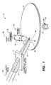
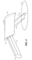
- Fig. 1 is a perspective view of a surface inspection system to illustrate the preferred embodiment of the invention.
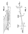
- Fig. 7 is a schematic view of the imaging optics, the CCD detectors and a portion of the surface to be inspected of the system of Fig. 1 taken along the line 7-7 in Fig. 2 to illustrate the operation of the system of Figs. 1-3 in response to height variation of the surface to illustrate the invention.
- Fig. 9 is a perspective view of a portion of a wafer inspection system employing a cylindrical mirror for illustrating another alternative embodiment of the invention.
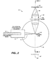
- Fig. 1 is a perspective view of a surface inspection system to illustrate the preferred embodiment of the invention.
- System 10 includes a cylindrical objective such as a cylindrical lens 12 for focusing a preferably collimated light beam 14 to a focused beam 16 for illuminating, on surface 18 to be inspected, an area in the shape of a line 20.
- Beam 14 and therefore also focused beam 16 are directed at an oblique angle of incidence to the surface 18.
- line 20 is substantially in the incidence plane or plane of incidence of focused beam 16.
- the incidence plane of beam 16 is defined by the common plane containing beam 16 and a normal direction such as 22 to surface 18 and passing through beam 16.
- the imaging subsystem 30 projects an image of a portion of the line 20 onto a corresponding detector in the CCD array 32 so that each detector in the array detects light from a corresponding portion of the line 20.
- the length of the line 20 is limited only by the size of the collimated input beam 14 and the physical aperture of lens or lens combination 12.
- an optional expander 34 shown in dotted lines may be used for controlling the diameter of beam 14 so as to control the length of line 20.
- the surface 18' to be inspected can also be moved by an XY stage 54 which moves the surface along the X and Y directions in order for line 20 to scan the entire surface.
- the illumination and collection portions of system 10' of Fig. 3 remain stationary. This is advantageous since it simplifies the optical alignment in the system, due to the fact that there is substantially no relative motion between the illumination portion and the collection portion of the system.
- the useful portion of the illumination line projected onto the CCD array 32 has a length of 5 mm
- the illumination line width W is 10 microns and array 32 has 500 elements with d equal to 10 microns and the scan line pitch is 5 microns
- the effective pixel size on the wafer is 5 microns x 10 microns, assuming that the image of the line at the array has the same length as the line.
- at least two or three samples are taken in each direction (along line 20 and normal to it) per effective optical spot size on the sample surface.
- reasonably high quality lenses such as quality camera lenses are used, such as ones having 5mm field of view, giving a 30° collection angle.
- the imaging subsystem 30 will also project an image of the CCD array 32 onto surface 18 overlapping that of line 20. This is illustrated in Fig. 6.
- imaging subsystem 30 will project an image 32A of the detector array on surface 18A, as shown in Fig. 6. But if the height of the surface is higher so that the surface is at 18B instead, then the imaging subsystem will project an image of the detector array at position 32B.
- the longer dimension of beam 16 is such that it illuminates both images 32A and 32B of the array.
- the imaging subsystem 30 will project the first detector in the array 32 to position 32A(1) on surface 18A, but to the position 32B(1) on position 18B of the surface as shown in Fig. 6.
- the two images are one on top of the other so that there is no lateral shift between them.
- an image of the same portion of surface 18 and, therefore, of line 20 will be focused to two different positions on the array 32, but the two positions will also be shifted only in the vertical direction but not laterally.
- the detectors cover both positions, then the variation in height between 18A, 18B of the surface will have no effect on the detection by array 32 and the system 10, 10' is tolerant of vertical height variations of the surface inspected.
- the imaging optics of subsystem 30 may be designed so that the change in height or vertical dimension of the projected image of line 20 onto the CCD array is within the height of the CCD array.
- the image of the line at the array 32 is longer than the array, and the extent of the height variations of the image of the line 20 on the detector array is such that the projected image still falls on the detector array.
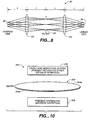
- Fig. 8 is a schematic view illustrating in more detail the imaging subsystem 30 of Figs. 1 and 2.
- Subsystem 30 preferably comprises two identical lenses: lens 102 for collecting light from line 20 and to perform Fourier transform, and lens 104 for imaging the line onto the array 32.
- the two lenses 102, 104 are preferably identical to minimize aberration.
- a filter and polarizer may be employed at position 106 where line 20, position 106 and array 32 appear at focal points of the two lenses 102, 104 each having a focal length f. Arranged in this manner, subsystem 30 minimizes aberration.
- a variable aperture may also be applied at a number of positions in subsystem 30 to control the portion of the line 20 that is focused onto array 32 by controlling the size of the aperture.
- An alternative method of generating a line focus on the sample is to use a cylindrical lens in the convention way, i.e. with its principal plane perpendicular to the propagation direction of the light beam 14, and placing a diffraction grating 252 immediately following the lens.
- the grating period is such that main diffraction angle matches the desired illumination angle range.
- the lens and the grating are held parallel to each other, and to the sample surface 18.
- the grating line structure (or grooves) are perpendicular to the focused line direction. The grating, therefore, will only have the effect of redirecting the light along the desired incidence angle.
- a variety of different grating types can be used, it is preferable to use a holographic type grating for its enhanced efficiency.
- the invention as described above may be used to provide a viable alternate mechanism to inspect rough films, patterned or unpatterned semiconductor wafers and backsides of wafers, as well as photomasks, reticles, liquid crystal displays or other flat panel displays.
- the system of this invention is compact, has a simple architecture, and provides a relatively low cost alternative for inspecting patterned wafers. Furthermore, because of the low cost of the system of this invention, it may also be advantageously used in conjunction with another surface inspection system for inspecting two different surfaces of an object, as illustrated in Fig. 10. Thus, as shown in Fig.
- a system 200 may include a front side inspection system 202 for inspecting the front side 204a of the semiconductor wafer 204, and a system 206 (which may be similar to that in Figs. 1, 2 or 3) for inspecting the backside 204b of the wafer. If, as in the invention described above, the illumination and light collection portions of the system remain stationary and the surface 204b is inspected by moving the surface, the two systems 202, 206 may need to be synchronized.
- System 202 may include a system such as that described above in reference to Figs. 1-3, or may be one of many different kinds of anomaly and surface feature inspection systems. All such variations are within the scope of the invention.
Abstract
Description
Claims (49)
- A method for detecting anomalies and/or features of a surface (18), comprising:providing a beam (16) of radiation at an oblique incidence angle to illuminate a line on the surface, said beam and a direction through the beam and normal to the surface defining an incidence plane of the beam, said line being substantially in the plane of incidence of the beam; andimaging said line onto an array (32) of detectors, each detector in the array detecting light from a corresponding portion of the line,said method characterised in that the providing provides a focused beam of radiation, focused to a line (20) on the surface.
- The method of claim 1, said providing including focusing the beam to a thin line on the surface.
- The method of claim 1, said imaging being such that an image of the line at said array is longer than the array.
- The method of claim 1, wherein said imaging images a centre part of the line onto said array.
- The method of claim 1, wherein said providing focuses the beam of radiation substantially only in a direction normal to the plane of incidence.
- The method of claim 5, said focusing including passing a beam of radiation though a cylindrical lens (12) or to a cylindrical mirror (112).
- The method of claim 1, further comprising controlling a cross-sectional dimension of the beam of radiation and said oblique incidence angle in order to select length of the illuminated line.
- The method of claim 7, said controlling including expanding a beam of radiation so that the beam has a desired diameter after expansion.
- The method of claim 1, wherein said imaging focuses the line along an axis that is substantially normal to the line.
- The method of claim 1, said imaging employing a variable aperture, said method further comprising controlling the aperture of the variable aperture in response to roughness on the surface.
- The method of claim 1, further comprising causing relative motion between the surface and the beam so that the line scans the surface to detect anomalies and/or a surface feature.
- The method of claim 9, wherein said causing moves the surface and leaves the beam and the array substantially stationary.
- The method of claim 1, said oblique angle being in a range of about 45 to 85 degrees from a normal direction to the surface.
- The method of claim 1, wherein said imaging employs an objective, and wherein the line is in a focus plane of the objective.
- The method of claim 1, further comprising performing time delayed integration at the array of detectors.
- The method of claim 1, wherein said imaging images said line onto an array of detectors outside of the plan of incidence.
- The method of claim 1, said array being shorter than an image of the line at the array formed by said imaging, wherein said imaging images a center part of the line onto said array.
- The method of claim 1, wherein said imaging causes an image of said line to fall onto said array of detectors despite changes in vertical position of the surface.
- The method of claim 1, said focusing including passing a beam of radiation through a cylindrical lens (12) that has a principal plane substantially parallel to the surface.
- The method of claim 1, said focusing including passing a beam of radiation to a cylindrical mirror (112) that has two substantially straight edges, wherein a plane defined by the two edges is substantially parallel to the surface.
- An apparatus for detecting anomalies of a surface (18) comprising:optics providing a beam (16) of radiation at an oblique incidence angle to illuminate a line on the surface, said beam and a direction through the beam and normal to the surface defining an incidence plane of the beam, said line being substantially in the plane of incidence of the beam;at least one array (32) of detectors; anda system imaging said line onto the at least one array of detectors, each detoctor in the at least one array detecting light from a corresponding portion of the line;said apparatus characterised in that the optics focuses the beam to the line (20).
- The apparatus of claim 21, wherein the optics focuses the beam to a thin line on the surface.
- The apparatus of claim 21, wherein an image of the line formed by the system at the array is longer than the array.
- The apparatus of claim 21, wherein said system images a center part of the line onto said array.
- The apparatus of claim 21, said optics focusing the beam substantially only in a direction normal to the plane of incidence.
- The apparatus of claim 25, said optics including a cylindrical lens (12) or a cylindrical mirror (112).
- The apparatus of claim 26, said optics including a cylindrical lens that has a principal plane substantially parallel to the surface.
- The apparatus of claim 27, wherein said optics focuses an input radiation beam directed at the optics, said input beam being substantially normal to the surface and to the lens, said focusing means further comprising a diffraction grating (252) for redirecting radiation from the lens towards the surface at an oblique angle to the surface.
- The apparatus of claim 25, wherein said optics focuses an input radiation beam directed at the optics, said input beam being in a direction oblique to the surface and to the principal plane of the lens.
- The apparatus of claim 24, said optics including a cylindrical mirror (112) that has two substantially straight edges, wherein a plane defined by the two edges is substantially parallel to the surface.
- The apparatus of claim 21, further comprising an expander (34) expanding the beam of radiation prior to focusing by the focusing means.
- The apparatus of claim 21, wherein said at least one array of detectors is outside of the plane of incidence.
- The apparatus of claim 21, wherein said system has an optical axis that is substantially normal to the line.
- The apparatus of claim 21, said system including a variable aperture for varying a collection angle of the system.
- The apparatus of claim 21, further comprising means for causing relative motion between the surface and the beam so that the line scans the surface to detect anomalies and/or a surface feature.
- The apparatus of claim 35, said at least one array of detectors being substantially stationary relative to the beam when relative motion is caused between the surface and the beam.
- The apparatus of claim 21, said oblique angle being in a range of about 45 to 85 degrees from a normal direction to the surface.
- The apparatus of claim 21, said at least one array of detectors being a linear array substantially parallel to the line.
- The apparatus of claim 21, said system comprising lens means having a Fourier plane, said apparatus further comprising a filter and polarizer substantially in the Fourier plane.
- The apparatus of claim 21, said at least one array being shorter than an image of the line at the array formed by the system, wherein said system images a center part of the line onto said array.
- The apparatus of claim 21 wherein a dimension of said array in a direction transverse to the focused line and/or imaging by said system causes an image of said line to fall onto said array of detectors despite changes in vertical position of the surface.
- The apparatus of claim 21, wherein a dimension of said array in a direction transverse to the line is such than an image of said line falls onto said array of detectors despite changes in vertical position of the surface.
- The apparatus of claim 41, wherein said system causes an image of said line to fall onto said array of detectors despite changes in vertical position of the surface.
- The apparatus of claim 21, wherein said at least one array of detectors is directly above the line (20).
- The apparatus of claim 21, further comprising a second array (32') of detectors.
- The apparatus of claim 21, wherein the second array is in a position opposite to the at least one array (32).
- An apparatus for detecting anomalies and/or a surface feature on a first and a second surface of an object, comprising:optics providing a beam (16) of radiation at an oblique incidence angle to illuminate a line on the first surface, said beam and a direction through the beam and normal to the first surface defining an incidence plane of the beam, said line being substantially in the plane of incidence of the beam;at least one array (32) of detectors;a system imaging said line onto the at least one array of detectors, each detector in the at least one array detecting light from a corresponding portion of the line; anda second detector detecting anomalies and/or a surface feature of the second surface, said apparatus characterised in that the optics focuses the beam to a focused line (20) on the first surface.
- The apparatus of claim 47, said first and second surfaces being on opposite sides of the object.
- The apparatus of claim 47, wherein said array of detectors is outside of the plane of incidence.
Applications Claiming Priority (3)
| Application Number | Priority Date | Filing Date | Title |
|---|---|---|---|
| US08/904,892 US6608676B1 (en) | 1997-08-01 | 1997-08-01 | System for detecting anomalies and/or features of a surface |
| US904892 | 1997-08-01 | ||
| PCT/US1998/016116 WO1999006823A1 (en) | 1997-08-01 | 1998-07-28 | System for detecting anomalies and/or features of a surface |
Publications (2)
| Publication Number | Publication Date |
|---|---|
| EP1000346A1 EP1000346A1 (en) | 2000-05-17 |
| EP1000346B1 true EP1000346B1 (en) | 2003-10-22 |
Family
ID=25419930
Family Applications (1)
| Application Number | Title | Priority Date | Filing Date |
|---|---|---|---|
| EP98939174A Expired - Lifetime EP1000346B1 (en) | 1997-08-01 | 1998-07-28 | System for detecting anomalies and/or features of a surface |
Country Status (7)
| Country | Link |
|---|---|
| US (5) | US6608676B1 (en) |
| EP (1) | EP1000346B1 (en) |
| JP (1) | JP4616472B2 (en) |
| AT (1) | ATE252731T1 (en) |
| AU (1) | AU8765798A (en) |
| DE (1) | DE69819159T2 (en) |
| WO (1) | WO1999006823A1 (en) |
Families Citing this family (97)
| Publication number | Priority date | Publication date | Assignee | Title |
|---|---|---|---|---|
| US6411377B1 (en) * | 1991-04-02 | 2002-06-25 | Hitachi, Ltd. | Optical apparatus for defect and particle size inspection |
| US6608676B1 (en) * | 1997-08-01 | 2003-08-19 | Kla-Tencor Corporation | System for detecting anomalies and/or features of a surface |
| US6091488A (en) * | 1999-03-22 | 2000-07-18 | Beltronics, Inc. | Method of and apparatus for automatic high-speed optical inspection of semi-conductor structures and the like through fluorescent photoresist inspection |
| US6587193B1 (en) * | 1999-05-11 | 2003-07-01 | Applied Materials, Inc. | Inspection systems performing two-dimensional imaging with line light spot |
| IL146386A (en) * | 2001-11-08 | 2010-02-17 | Nova Measuring Instr Ltd | Method and apparatus for measuring thin films |
| US20040032581A1 (en) * | 2002-01-15 | 2004-02-19 | Mehrdad Nikoonahad | Systems and methods for inspection of specimen surfaces |
| US7088443B2 (en) * | 2002-02-11 | 2006-08-08 | Kla-Tencor Technologies Corporation | System for detecting anomalies and/or features of a surface |
| US6724473B2 (en) | 2002-03-27 | 2004-04-20 | Kla-Tencor Technologies Corporation | Method and system using exposure control to inspect a surface |
| US20040042001A1 (en) | 2002-04-18 | 2004-03-04 | Kla-Tencor Technologies Corporation | Simultaneous multi-spot inspection and imaging |
| US7130039B2 (en) * | 2002-04-18 | 2006-10-31 | Kla-Tencor Technologies Corporation | Simultaneous multi-spot inspection and imaging |
| US20070258085A1 (en) * | 2006-05-02 | 2007-11-08 | Robbins Michael D | Substrate illumination and inspection system |
| DE10232781B4 (en) * | 2002-07-18 | 2013-03-28 | Vistec Semiconductor Systems Gmbh | Device for wafer inspection |
| US7068363B2 (en) * | 2003-06-06 | 2006-06-27 | Kla-Tencor Technologies Corp. | Systems for inspection of patterned or unpatterned wafers and other specimen |
| JP4536337B2 (en) * | 2003-06-10 | 2010-09-01 | 株式会社トプコン | Surface inspection method and surface inspection apparatus |
| US7365834B2 (en) * | 2003-06-24 | 2008-04-29 | Kla-Tencor Technologies Corporation | Optical system for detecting anomalies and/or features of surfaces |
| JP4641143B2 (en) * | 2003-06-30 | 2011-03-02 | 株式会社トプコン | Surface inspection device |
| US7280200B2 (en) * | 2003-07-18 | 2007-10-09 | Ade Corporation | Detection of a wafer edge using collimated light |
| US7130036B1 (en) * | 2003-09-16 | 2006-10-31 | Kla-Tencor Technologies Corp. | Methods and systems for inspection of an entire wafer surface using multiple detection channels |
| US7265809B2 (en) * | 2003-10-07 | 2007-09-04 | Universal Avionics Systems Corporation | Flat panel display having integral metal heater optically hidden behind an EMI shield |
| WO2006012058A1 (en) * | 2004-06-28 | 2006-02-02 | Japan Communications, Inc. | Systems and methods for mutual authentication of network |
| WO2006014152A1 (en) * | 2004-07-01 | 2006-02-09 | Midwest Research Institute | Optic probe for semiconductor characterization |
| US7233389B2 (en) * | 2004-12-03 | 2007-06-19 | Omnitek Partners, Llc | System and method for the measurement of the velocity and acceleration of objects |
| US7253376B2 (en) * | 2005-01-21 | 2007-08-07 | Ultratech, Inc. | Methods and apparatus for truncating an image formed with coherent radiation |
| US7804993B2 (en) * | 2005-02-28 | 2010-09-28 | Applied Materials South East Asia Pte. Ltd. | Method and apparatus for detecting defects in wafers including alignment of the wafer images so as to induce the same smear in all images |
| US7315361B2 (en) * | 2005-04-29 | 2008-01-01 | Gsi Group Corporation | System and method for inspecting wafers in a laser marking system |
| JP4988223B2 (en) | 2005-06-22 | 2012-08-01 | 株式会社日立ハイテクノロジーズ | Defect inspection apparatus and method |
| US7345754B1 (en) | 2005-09-16 | 2008-03-18 | Kla-Tencor Technologies Corp. | Fourier filters and wafer inspection systems |
| US20070119836A1 (en) * | 2005-11-29 | 2007-05-31 | Thomas Schroeder | Method and apparatus for focusing a beam from an excimer laser to form a line of light on a substrate |
| JP4996856B2 (en) | 2006-01-23 | 2012-08-08 | 株式会社日立ハイテクノロジーズ | Defect inspection apparatus and method |
| US20070229833A1 (en) * | 2006-02-22 | 2007-10-04 | Allan Rosencwaig | High-sensitivity surface detection system and method |
| US9068917B1 (en) * | 2006-03-14 | 2015-06-30 | Kla-Tencor Technologies Corp. | Systems and methods for inspection of a specimen |
| JP2007248086A (en) | 2006-03-14 | 2007-09-27 | Hitachi High-Technologies Corp | Flaw inspection device |
| US7508504B2 (en) * | 2006-05-02 | 2009-03-24 | Accretech Usa, Inc. | Automatic wafer edge inspection and review system |
| US20090122304A1 (en) * | 2006-05-02 | 2009-05-14 | Accretech Usa, Inc. | Apparatus and Method for Wafer Edge Exclusion Measurement |
| US20090116727A1 (en) * | 2006-05-02 | 2009-05-07 | Accretech Usa, Inc. | Apparatus and Method for Wafer Edge Defects Detection |
| US7433033B2 (en) * | 2006-05-05 | 2008-10-07 | Asml Netherlands B.V. | Inspection method and apparatus using same |
| US7525649B1 (en) * | 2007-10-19 | 2009-04-28 | Kla-Tencor Technologies Corporation | Surface inspection system using laser line illumination with two dimensional imaging |
| US7826049B2 (en) * | 2008-02-11 | 2010-11-02 | Applied Materials South East Asia Pte. Ltd. | Inspection tools supporting multiple operating states for multiple detector arrangements |
| JP5319930B2 (en) | 2008-02-20 | 2013-10-16 | 株式会社日立ハイテクノロジーズ | Defect inspection apparatus and defect inspection method |
| US8285025B2 (en) * | 2008-03-25 | 2012-10-09 | Electro Scientific Industries, Inc. | Method and apparatus for detecting defects using structured light |
| US7973921B2 (en) * | 2008-06-25 | 2011-07-05 | Applied Materials South East Asia Pte Ltd. | Dynamic illumination in optical inspection systems |
| NL2003658A (en) * | 2008-12-31 | 2010-07-01 | Asml Holding Nv | Euv mask inspection. |
| JP5331586B2 (en) | 2009-06-18 | 2013-10-30 | 株式会社日立ハイテクノロジーズ | Defect inspection apparatus and inspection method |
| JP5405956B2 (en) | 2009-09-24 | 2014-02-05 | 株式会社日立ハイテクノロジーズ | Defect inspection equipment |
| JP5538072B2 (en) | 2010-06-03 | 2014-07-02 | 株式会社日立ハイテクノロジーズ | Defect inspection method and apparatus |
| JP5520737B2 (en) | 2010-07-30 | 2014-06-11 | 株式会社日立ハイテクノロジーズ | Defect inspection apparatus and defect inspection method |
| JP5259669B2 (en) * | 2010-09-27 | 2013-08-07 | 株式会社日立ハイテクノロジーズ | Defect inspection apparatus and defect inspection method |
| JP2012127682A (en) | 2010-12-13 | 2012-07-05 | Hitachi High-Technologies Corp | Defect inspection method and device therefor |
| JP2012137350A (en) | 2010-12-27 | 2012-07-19 | Hitachi High-Technologies Corp | Defect inspection method and device |
| US8885158B2 (en) * | 2011-03-10 | 2014-11-11 | Kla-Tencor Corporation | Surface scanning inspection system with adjustable scan pitch |
| US9793673B2 (en) | 2011-06-13 | 2017-10-17 | Kla-Tencor Corporation | Semiconductor inspection and metrology system using laser pulse multiplier |
| US8873596B2 (en) | 2011-07-22 | 2014-10-28 | Kla-Tencor Corporation | Laser with high quality, stable output beam, and long life high conversion efficiency non-linear crystal |
| US9250178B2 (en) | 2011-10-07 | 2016-02-02 | Kla-Tencor Corporation | Passivation of nonlinear optical crystals |
| CN102489875A (en) * | 2011-11-25 | 2012-06-13 | 中国航空工业集团公司北京航空制造工程研究所 | Laser oblique incidence energy compensation method by using cylindrical mirror |
| WO2013080209A1 (en) | 2011-12-01 | 2013-06-06 | P.M.L. - Particles Monitoring Technologies Ltd. | Detection scheme for particle size and concentration measurement |
| JPWO2013099468A1 (en) | 2011-12-27 | 2015-04-30 | 株式会社日立ハイテクノロジーズ | Inspection device |
| JP5865738B2 (en) | 2012-03-13 | 2016-02-17 | 株式会社日立ハイテクノロジーズ | Defect inspection method and apparatus |
| US9496425B2 (en) | 2012-04-10 | 2016-11-15 | Kla-Tencor Corporation | Back-illuminated sensor with boron layer |
| KR20140117640A (en) * | 2012-05-16 | 2014-10-07 | 가부시키가이샤 히다치 하이테크놀로지즈 | Inspection device |
| US9601299B2 (en) | 2012-08-03 | 2017-03-21 | Kla-Tencor Corporation | Photocathode including silicon substrate with boron layer |
| US9086389B2 (en) | 2012-10-26 | 2015-07-21 | Kla-Tencor Corporation | Sample inspection system detector |
| US9151940B2 (en) | 2012-12-05 | 2015-10-06 | Kla-Tencor Corporation | Semiconductor inspection and metrology system using laser pulse multiplier |
| US9426400B2 (en) | 2012-12-10 | 2016-08-23 | Kla-Tencor Corporation | Method and apparatus for high speed acquisition of moving images using pulsed illumination |
| US8929406B2 (en) | 2013-01-24 | 2015-01-06 | Kla-Tencor Corporation | 193NM laser and inspection system |
| US9529182B2 (en) | 2013-02-13 | 2016-12-27 | KLA—Tencor Corporation | 193nm laser and inspection system |
| US9608399B2 (en) | 2013-03-18 | 2017-03-28 | Kla-Tencor Corporation | 193 nm laser and an inspection system using a 193 nm laser |
| US9478402B2 (en) | 2013-04-01 | 2016-10-25 | Kla-Tencor Corporation | Photomultiplier tube, image sensor, and an inspection system using a PMT or image sensor |
| US9347890B2 (en) | 2013-12-19 | 2016-05-24 | Kla-Tencor Corporation | Low-noise sensor and an inspection system using a low-noise sensor |
| US9748294B2 (en) | 2014-01-10 | 2017-08-29 | Hamamatsu Photonics K.K. | Anti-reflection layer for back-illuminated sensor |
| US9410901B2 (en) | 2014-03-17 | 2016-08-09 | Kla-Tencor Corporation | Image sensor, an inspection system and a method of inspecting an article |
| US9804101B2 (en) | 2014-03-20 | 2017-10-31 | Kla-Tencor Corporation | System and method for reducing the bandwidth of a laser and an inspection system and method using a laser |
| GB2526866A (en) * | 2014-06-05 | 2015-12-09 | Univ Bristol | Apparatus for and method of inspecting surface topography of a moving object |
| US9525265B2 (en) | 2014-06-20 | 2016-12-20 | Kla-Tencor Corporation | Laser repetition rate multiplier and flat-top beam profile generators using mirrors and/or prisms |
| KR102316146B1 (en) | 2014-08-13 | 2021-10-22 | 삼성전자주식회사 | Optical module for surface inspection and surface inspection apparatus including the same |
| US9767986B2 (en) | 2014-08-29 | 2017-09-19 | Kla-Tencor Corporation | Scanning electron microscope and methods of inspecting and reviewing samples |
| US9419407B2 (en) | 2014-09-25 | 2016-08-16 | Kla-Tencor Corporation | Laser assembly and inspection system using monolithic bandwidth narrowing apparatus |
| US9891177B2 (en) | 2014-10-03 | 2018-02-13 | Kla-Tencor Corporation | TDI sensor in a darkfield system |
| US9748729B2 (en) | 2014-10-03 | 2017-08-29 | Kla-Tencor Corporation | 183NM laser and inspection system |
| JP6635674B2 (en) * | 2015-05-11 | 2020-01-29 | キヤノン株式会社 | Measuring device, measuring method and program |
| US9860466B2 (en) | 2015-05-14 | 2018-01-02 | Kla-Tencor Corporation | Sensor with electrically controllable aperture for inspection and metrology systems |
| US10748730B2 (en) | 2015-05-21 | 2020-08-18 | Kla-Tencor Corporation | Photocathode including field emitter array on a silicon substrate with boron layer |
| US10462391B2 (en) | 2015-08-14 | 2019-10-29 | Kla-Tencor Corporation | Dark-field inspection using a low-noise sensor |
| US10778925B2 (en) | 2016-04-06 | 2020-09-15 | Kla-Tencor Corporation | Multiple column per channel CCD sensor architecture for inspection and metrology |
| US10313622B2 (en) | 2016-04-06 | 2019-06-04 | Kla-Tencor Corporation | Dual-column-parallel CCD sensor and inspection systems using a sensor |
| US10324045B2 (en) | 2016-08-05 | 2019-06-18 | Kla-Tencor Corporation | Surface defect inspection with large particle monitoring and laser power control |
| US10739275B2 (en) * | 2016-09-15 | 2020-08-11 | Kla-Tencor Corporation | Simultaneous multi-directional laser wafer inspection |
| US10175555B2 (en) | 2017-01-03 | 2019-01-08 | KLA—Tencor Corporation | 183 nm CW laser and inspection system |
| CN111247418A (en) | 2017-10-26 | 2020-06-05 | 粒子监测系统有限公司 | Particle measurement system and method |
| US11114489B2 (en) | 2018-06-18 | 2021-09-07 | Kla-Tencor Corporation | Back-illuminated sensor and a method of manufacturing a sensor |
| US10943760B2 (en) | 2018-10-12 | 2021-03-09 | Kla Corporation | Electron gun and electron microscope |
| US11114491B2 (en) | 2018-12-12 | 2021-09-07 | Kla Corporation | Back-illuminated sensor and a method of manufacturing a sensor |
| EP3959505A4 (en) | 2019-04-25 | 2023-06-07 | Particle Measuring Systems, Inc. | Particle detection systems and methods for on-axis particle detection and/or differential detection |
| WO2020257154A1 (en) * | 2019-06-17 | 2020-12-24 | Georgia Tech Research Corporation | Low-aberration high-speed-compatible optical delay lines and methods thereof |
| US11703460B2 (en) | 2019-07-09 | 2023-07-18 | Kla Corporation | Methods and systems for optical surface defect material characterization |
| US11668601B2 (en) * | 2020-02-24 | 2023-06-06 | Kla Corporation | Instrumented substrate apparatus |
| US11848350B2 (en) | 2020-04-08 | 2023-12-19 | Kla Corporation | Back-illuminated sensor and a method of manufacturing a sensor using a silicon on insulator wafer |
| CN115201990A (en) * | 2022-09-08 | 2022-10-18 | 成都中科卓尔智能科技集团有限公司 | Light source lens of semiconductor optical material internal defect detection sheet |
Family Cites Families (47)
| Publication number | Priority date | Publication date | Assignee | Title |
|---|---|---|---|---|
| US4353649A (en) * | 1979-07-06 | 1982-10-12 | Tokyo Shibaura Denki Kabushiki Kaisha | Apparatus for surface stress measurement of glass coating and transparent plastic product |
| JPS5630630A (en) * | 1979-08-23 | 1981-03-27 | Hitachi Ltd | Foreign matter detector |
| US4579455A (en) | 1983-05-09 | 1986-04-01 | Kla Instruments Corporation | Photomask inspection apparatus and method with improved defect detection |
| JPH0750664B2 (en) * | 1983-06-23 | 1995-05-31 | 富士通株式会社 | Reticle inspection method |
| US4629319A (en) * | 1984-02-14 | 1986-12-16 | Diffracto Ltd. | Panel surface flaw inspection |
| GB2159271B (en) * | 1984-04-27 | 1988-05-18 | Nissan Motor | Surface flaw detecting method and apparatus |
| US4795911A (en) * | 1986-02-14 | 1989-01-03 | Canon Kabushiki Kaisha | Surface examining apparatus for detecting the presence of foreign particles on the surface |
| JPS6333834A (en) * | 1986-07-28 | 1988-02-13 | Canon Inc | Surface state inspecting apparatus |
| DE3637477A1 (en) | 1986-11-04 | 1988-05-11 | Wacker Chemitronic | METHOD AND DEVICE FOR DETERMINING THE QUALITY OF SURFACES, IN PARTICULAR OF SEMICONDUCTOR DISC |
| JPS63314963A (en) | 1987-06-18 | 1988-12-22 | Fuji Photo Film Co Ltd | Original illuminator |
| US4898471A (en) | 1987-06-18 | 1990-02-06 | Tencor Instruments | Particle detection on patterned wafers and the like |
| JP2512059B2 (en) * | 1988-02-26 | 1996-07-03 | 株式会社日立製作所 | Foreign object detection method and apparatus |
| US5206699A (en) | 1988-05-06 | 1993-04-27 | Gersan Establishment | Sensing a narrow frequency band of radiation and gemstones |
| US5274434A (en) * | 1990-04-02 | 1993-12-28 | Hitachi, Ltd. | Method and apparatus for inspecting foreign particles on real time basis in semiconductor mass production line |
| US5237404A (en) * | 1990-06-28 | 1993-08-17 | Mazda Motor Corporation | Inspection apparatus with improved detection of surface defects over large and curved surfaces |
| US5192856A (en) | 1990-11-19 | 1993-03-09 | An Con Genetics, Inc. | Auto focusing bar code reader |
| US5172005A (en) * | 1991-02-20 | 1992-12-15 | Pressco Technology, Inc. | Engineered lighting system for tdi inspection comprising means for controlling lighting elements in accordance with specimen displacement |
| US5463459A (en) | 1991-04-02 | 1995-10-31 | Hitachi, Ltd. | Method and apparatus for analyzing the state of generation of foreign particles in semiconductor fabrication process |
| US6411377B1 (en) * | 1991-04-02 | 2002-06-25 | Hitachi, Ltd. | Optical apparatus for defect and particle size inspection |
| US5479259A (en) | 1991-05-20 | 1995-12-26 | Hitachi, Ltd. | Method and apparatus for detecting photoacoustic signal |
| US5251010A (en) * | 1991-06-07 | 1993-10-05 | Glasstech, Inc. | Optical roller wave gauge |
| US5636187A (en) * | 1992-12-11 | 1997-06-03 | Canon Kabushiki Kaisha | Magnetooptical recording apparatus and magnetooptical recording method for canceling leakage magnetic fields associated with a recording medium and devices ancillary to the recording medium |
| JPH06194320A (en) * | 1992-12-25 | 1994-07-15 | Hitachi Ltd | Method and equipment for inspecting mirror face substrate in semiconductor manufacturing line and method for manufacturing |
| JP3599630B2 (en) | 1993-03-09 | 2004-12-08 | 株式会社ルネサステクノロジ | Defect inspection method and defect inspection device |
| JP3599631B2 (en) | 1993-03-09 | 2004-12-08 | 株式会社ルネサステクノロジ | Defect inspection method and defect inspection device |
| JP3435187B2 (en) * | 1993-05-12 | 2003-08-11 | 株式会社日立製作所 | Defect inspection method and apparatus |
| JP3253177B2 (en) * | 1993-06-15 | 2002-02-04 | キヤノン株式会社 | Surface condition inspection device |
| US5663569A (en) * | 1993-10-14 | 1997-09-02 | Nikon Corporation | Defect inspection method and apparatus, and defect display method |
| US5463549A (en) * | 1993-10-15 | 1995-10-31 | Schlumberger Technology Corporation | Method and apparatus for determining permeability of subsurface formations |
| JPH07209202A (en) * | 1994-01-21 | 1995-08-11 | Canon Inc | Surface state inspection equipment, exposure apparatus employing it, and production of device using the exposure apparatus |
| JPH07318504A (en) * | 1994-05-23 | 1995-12-08 | Hitachi Electron Eng Co Ltd | Foreign matter detecting light receiving system for wafer |
| US5864394A (en) * | 1994-06-20 | 1999-01-26 | Kla-Tencor Corporation | Surface inspection system |
| US5883710A (en) * | 1994-12-08 | 1999-03-16 | Kla-Tencor Corporation | Scanning system for inspecting anomalies on surfaces |
| US5530550A (en) * | 1994-12-21 | 1996-06-25 | Tencor Instruments | Optical wafer positioning system |
| US5576831A (en) * | 1994-06-20 | 1996-11-19 | Tencor Instruments | Wafer alignment sensor |
| US6118525A (en) * | 1995-03-06 | 2000-09-12 | Ade Optical Systems Corporation | Wafer inspection system for distinguishing pits and particles |
| JP3140664B2 (en) | 1995-06-30 | 2001-03-05 | 松下電器産業株式会社 | Foreign matter inspection method and apparatus |
| JP3668294B2 (en) * | 1995-08-22 | 2005-07-06 | オリンパス株式会社 | Surface defect inspection equipment |
| US5825482A (en) | 1995-09-29 | 1998-10-20 | Kla-Tencor Corporation | Surface inspection system with misregistration error correction and adaptive illumination |
| US5644393A (en) | 1995-10-19 | 1997-07-01 | Hitachi Electronics Engineering Co., Ltd. | Extraneous substance inspection method and apparatus |
| US5737074A (en) * | 1995-12-05 | 1998-04-07 | New Creation Co., Ltd. | Surface inspection method and apparatus |
| US5926266A (en) * | 1996-09-23 | 1999-07-20 | International Business Machines Corporation | Optical apparatus for rapid defect analysis |
| US5719840A (en) | 1996-12-30 | 1998-02-17 | Phase Metrics | Optical sensor with an elliptical illumination spot |
| JPH10318504A (en) * | 1997-05-16 | 1998-12-04 | Babcock Hitachi Kk | High capacity pulverized solid fuel burner |
| US6608676B1 (en) * | 1997-08-01 | 2003-08-19 | Kla-Tencor Corporation | System for detecting anomalies and/or features of a surface |
| JPH11230915A (en) | 1998-02-13 | 1999-08-27 | Hitachi Ltd | Foreign-body inspection apparatus |
| US7088443B2 (en) * | 2002-02-11 | 2006-08-08 | Kla-Tencor Technologies Corporation | System for detecting anomalies and/or features of a surface |
-
1997
- 1997-08-01 US US08/904,892 patent/US6608676B1/en not_active Expired - Lifetime
-
1998
- 1998-07-28 AT AT98939174T patent/ATE252731T1/en not_active IP Right Cessation
- 1998-07-28 AU AU87657/98A patent/AU8765798A/en not_active Abandoned
- 1998-07-28 EP EP98939174A patent/EP1000346B1/en not_active Expired - Lifetime
- 1998-07-28 DE DE69819159T patent/DE69819159T2/en not_active Expired - Lifetime
- 1998-07-28 WO PCT/US1998/016116 patent/WO1999006823A1/en active IP Right Grant
- 1998-07-28 JP JP2000505506A patent/JP4616472B2/en not_active Expired - Lifetime
-
2003
- 2003-05-30 US US10/452,624 patent/US20040036864A1/en not_active Abandoned
-
2004
- 2004-09-24 US US10/949,078 patent/US7280199B2/en not_active Expired - Fee Related
-
2007
- 2007-09-14 US US11/855,935 patent/US20080002193A1/en not_active Abandoned
-
2008
- 2008-05-19 US US12/123,393 patent/US7869023B2/en not_active Expired - Fee Related
Also Published As
| Publication number | Publication date |
|---|---|
| WO1999006823A1 (en) | 1999-02-11 |
| US6608676B1 (en) | 2003-08-19 |
| US7280199B2 (en) | 2007-10-09 |
| US20080002193A1 (en) | 2008-01-03 |
| AU8765798A (en) | 1999-02-22 |
| US20040036864A1 (en) | 2004-02-26 |
| DE69819159T2 (en) | 2004-06-17 |
| JP4616472B2 (en) | 2011-01-19 |
| EP1000346A1 (en) | 2000-05-17 |
| ATE252731T1 (en) | 2003-11-15 |
| US20080218762A1 (en) | 2008-09-11 |
| JP2001512237A (en) | 2001-08-21 |
| US7869023B2 (en) | 2011-01-11 |
| US20050036138A1 (en) | 2005-02-17 |
| DE69819159D1 (en) | 2003-11-27 |
Similar Documents
| Publication | Publication Date | Title |
|---|---|---|
| EP1000346B1 (en) | System for detecting anomalies and/or features of a surface | |
| US7088443B2 (en) | System for detecting anomalies and/or features of a surface | |
| US7679735B2 (en) | Optical system for detecting anomalies and/or features of surfaces | |
| US7525649B1 (en) | Surface inspection system using laser line illumination with two dimensional imaging | |
| US7859656B2 (en) | Defect inspection method and system | |
| US7477372B2 (en) | Optical scanning system for surface inspection | |
| US7259869B2 (en) | System and method for performing bright field and dark field optical inspection | |
| US7227984B2 (en) | Method and apparatus for identifying defects in a substrate surface by using dithering to reconstruct under-sampled images | |
| US5659390A (en) | Method and apparatus for detecting particles on a surface of a semiconductor wafer having repetitive patterns | |
| WO2011036838A1 (en) | Flaw inspecting method and device therefor | |
| JP3453128B2 (en) | Optical scanning device and defect detection device | |
| JP2539182B2 (en) | Foreign matter inspection method on semiconductor wafer | |
| JPH0731129B2 (en) | Semiconductor wafer particle detector |
Legal Events
| Date | Code | Title | Description |
|---|---|---|---|
| PUAI | Public reference made under article 153(3) epc to a published international application that has entered the european phase |
Free format text: ORIGINAL CODE: 0009012 |
|
| 17P | Request for examination filed |
Effective date: 20000301 |
|
| AK | Designated contracting states |
Kind code of ref document: A1 Designated state(s): AT BE CH CY DE DK ES FI FR GB GR IE IT LI LU MC NL PT SE |
|
| 17Q | First examination report despatched |
Effective date: 20020218 |
|
| GRAH | Despatch of communication of intention to grant a patent |
Free format text: ORIGINAL CODE: EPIDOS IGRA |
|
| GRAS | Grant fee paid |
Free format text: ORIGINAL CODE: EPIDOSNIGR3 |
|
| GRAA | (expected) grant |
Free format text: ORIGINAL CODE: 0009210 |
|
| AK | Designated contracting states |
Kind code of ref document: B1 Designated state(s): AT BE CH CY DE DK ES FI FR GB GR IE IT LI LU MC NL PT SE |
|
| PG25 | Lapsed in a contracting state [announced via postgrant information from national office to epo] |
Ref country code: NL Free format text: LAPSE BECAUSE OF FAILURE TO SUBMIT A TRANSLATION OF THE DESCRIPTION OR TO PAY THE FEE WITHIN THE PRESCRIBED TIME-LIMIT Effective date: 20031022 Ref country code: LI Free format text: LAPSE BECAUSE OF FAILURE TO SUBMIT A TRANSLATION OF THE DESCRIPTION OR TO PAY THE FEE WITHIN THE PRESCRIBED TIME-LIMIT Effective date: 20031022 Ref country code: IT Free format text: LAPSE BECAUSE OF FAILURE TO SUBMIT A TRANSLATION OF THE DESCRIPTION OR TO PAY THE FEE WITHIN THE PRESCRIBED TIME-LIMIT;WARNING: LAPSES OF ITALIAN PATENTS WITH EFFECTIVE DATE BEFORE 2007 MAY HAVE OCCURRED AT ANY TIME BEFORE 2007. THE CORRECT EFFECTIVE DATE MAY BE DIFFERENT FROM THE ONE RECORDED. Effective date: 20031022 Ref country code: FI Free format text: LAPSE BECAUSE OF FAILURE TO SUBMIT A TRANSLATION OF THE DESCRIPTION OR TO PAY THE FEE WITHIN THE PRESCRIBED TIME-LIMIT Effective date: 20031022 Ref country code: CY Free format text: LAPSE BECAUSE OF FAILURE TO SUBMIT A TRANSLATION OF THE DESCRIPTION OR TO PAY THE FEE WITHIN THE PRESCRIBED TIME-LIMIT Effective date: 20031022 Ref country code: CH Free format text: LAPSE BECAUSE OF FAILURE TO SUBMIT A TRANSLATION OF THE DESCRIPTION OR TO PAY THE FEE WITHIN THE PRESCRIBED TIME-LIMIT Effective date: 20031022 Ref country code: BE Free format text: LAPSE BECAUSE OF FAILURE TO SUBMIT A TRANSLATION OF THE DESCRIPTION OR TO PAY THE FEE WITHIN THE PRESCRIBED TIME-LIMIT Effective date: 20031022 Ref country code: AT Free format text: LAPSE BECAUSE OF FAILURE TO SUBMIT A TRANSLATION OF THE DESCRIPTION OR TO PAY THE FEE WITHIN THE PRESCRIBED TIME-LIMIT Effective date: 20031022 |
|
| REG | Reference to a national code |
Ref country code: GB Ref legal event code: FG4D |
|
| REG | Reference to a national code |
Ref country code: CH Ref legal event code: EP |
|
| REG | Reference to a national code |
Ref country code: IE Ref legal event code: FG4D |
|
| REF | Corresponds to: |
Ref document number: 69819159 Country of ref document: DE Date of ref document: 20031127 Kind code of ref document: P |
|
| PG25 | Lapsed in a contracting state [announced via postgrant information from national office to epo] |
Ref country code: SE Free format text: LAPSE BECAUSE OF FAILURE TO SUBMIT A TRANSLATION OF THE DESCRIPTION OR TO PAY THE FEE WITHIN THE PRESCRIBED TIME-LIMIT Effective date: 20040122 Ref country code: GR Free format text: LAPSE BECAUSE OF FAILURE TO SUBMIT A TRANSLATION OF THE DESCRIPTION OR TO PAY THE FEE WITHIN THE PRESCRIBED TIME-LIMIT Effective date: 20040122 Ref country code: DK Free format text: LAPSE BECAUSE OF FAILURE TO SUBMIT A TRANSLATION OF THE DESCRIPTION OR TO PAY THE FEE WITHIN THE PRESCRIBED TIME-LIMIT Effective date: 20040122 |
|
| PG25 | Lapsed in a contracting state [announced via postgrant information from national office to epo] |
Ref country code: ES Free format text: LAPSE BECAUSE OF FAILURE TO SUBMIT A TRANSLATION OF THE DESCRIPTION OR TO PAY THE FEE WITHIN THE PRESCRIBED TIME-LIMIT Effective date: 20040202 |
|
| NLV1 | Nl: lapsed or annulled due to failure to fulfill the requirements of art. 29p and 29m of the patents act | ||
| REG | Reference to a national code |
Ref country code: CH Ref legal event code: PL |
|
| PG25 | Lapsed in a contracting state [announced via postgrant information from national office to epo] |
Ref country code: LU Free format text: LAPSE BECAUSE OF NON-PAYMENT OF DUE FEES Effective date: 20040728 Ref country code: IE Free format text: LAPSE BECAUSE OF NON-PAYMENT OF DUE FEES Effective date: 20040728 |
|
| ET | Fr: translation filed | ||
| PG25 | Lapsed in a contracting state [announced via postgrant information from national office to epo] |
Ref country code: MC Free format text: LAPSE BECAUSE OF NON-PAYMENT OF DUE FEES Effective date: 20040731 |
|
| PLBE | No opposition filed within time limit |
Free format text: ORIGINAL CODE: 0009261 |
|
| STAA | Information on the status of an ep patent application or granted ep patent |
Free format text: STATUS: NO OPPOSITION FILED WITHIN TIME LIMIT |
|
| 26N | No opposition filed |
Effective date: 20040723 |
|
| REG | Reference to a national code |
Ref country code: IE Ref legal event code: MM4A |
|
| PG25 | Lapsed in a contracting state [announced via postgrant information from national office to epo] |
Ref country code: PT Free format text: LAPSE BECAUSE OF NON-PAYMENT OF DUE FEES Effective date: 20040322 |
|
| PGFP | Annual fee paid to national office [announced via postgrant information from national office to epo] |
Ref country code: GB Payment date: 20140729 Year of fee payment: 17 Ref country code: FR Payment date: 20140717 Year of fee payment: 17 |
|
| GBPC | Gb: european patent ceased through non-payment of renewal fee |
Effective date: 20150728 |
|
| PG25 | Lapsed in a contracting state [announced via postgrant information from national office to epo] |
Ref country code: GB Free format text: LAPSE BECAUSE OF NON-PAYMENT OF DUE FEES Effective date: 20150728 |
|
| REG | Reference to a national code |
Ref country code: FR Ref legal event code: ST Effective date: 20160331 |
|
| PG25 | Lapsed in a contracting state [announced via postgrant information from national office to epo] |
Ref country code: FR Free format text: LAPSE BECAUSE OF NON-PAYMENT OF DUE FEES Effective date: 20150731 |
|
| PGFP | Annual fee paid to national office [announced via postgrant information from national office to epo] |
Ref country code: DE Payment date: 20170727 Year of fee payment: 20 |
|
| REG | Reference to a national code |
Ref country code: DE Ref legal event code: R071 Ref document number: 69819159 Country of ref document: DE |
|
| P01 | Opt-out of the competence of the unified patent court (upc) registered |
Effective date: 20230525 |