EP1005121A2 - Laser driving apparatus, driving method thereof, and image-forming apparatus using it - Google Patents
Laser driving apparatus, driving method thereof, and image-forming apparatus using it Download PDFInfo
- Publication number
- EP1005121A2 EP1005121A2 EP99123349A EP99123349A EP1005121A2 EP 1005121 A2 EP1005121 A2 EP 1005121A2 EP 99123349 A EP99123349 A EP 99123349A EP 99123349 A EP99123349 A EP 99123349A EP 1005121 A2 EP1005121 A2 EP 1005121A2
- Authority
- EP
- European Patent Office
- Prior art keywords
- current
- laser
- voltage
- light
- common
- Prior art date
- Legal status (The legal status is an assumption and is not a legal conclusion. Google has not performed a legal analysis and makes no representation as to the accuracy of the status listed.)
- Granted
Links
Images


Classifications
-
- H—ELECTRICITY
- H01—ELECTRIC ELEMENTS
- H01S—DEVICES USING THE PROCESS OF LIGHT AMPLIFICATION BY STIMULATED EMISSION OF RADIATION [LASER] TO AMPLIFY OR GENERATE LIGHT; DEVICES USING STIMULATED EMISSION OF ELECTROMAGNETIC RADIATION IN WAVE RANGES OTHER THAN OPTICAL
- H01S5/00—Semiconductor lasers
- H01S5/06—Arrangements for controlling the laser output parameters, e.g. by operating on the active medium
- H01S5/068—Stabilisation of laser output parameters
- H01S5/0683—Stabilisation of laser output parameters by monitoring the optical output parameters
-
- H—ELECTRICITY
- H01—ELECTRIC ELEMENTS
- H01S—DEVICES USING THE PROCESS OF LIGHT AMPLIFICATION BY STIMULATED EMISSION OF RADIATION [LASER] TO AMPLIFY OR GENERATE LIGHT; DEVICES USING STIMULATED EMISSION OF ELECTROMAGNETIC RADIATION IN WAVE RANGES OTHER THAN OPTICAL
- H01S5/00—Semiconductor lasers
- H01S5/04—Processes or apparatus for excitation, e.g. pumping, e.g. by electron beams
- H01S5/042—Electrical excitation ; Circuits therefor
-
- H—ELECTRICITY
- H01—ELECTRIC ELEMENTS
- H01S—DEVICES USING THE PROCESS OF LIGHT AMPLIFICATION BY STIMULATED EMISSION OF RADIATION [LASER] TO AMPLIFY OR GENERATE LIGHT; DEVICES USING STIMULATED EMISSION OF ELECTROMAGNETIC RADIATION IN WAVE RANGES OTHER THAN OPTICAL
- H01S5/00—Semiconductor lasers
- H01S5/06—Arrangements for controlling the laser output parameters, e.g. by operating on the active medium
- H01S5/068—Stabilisation of laser output parameters
- H01S5/0683—Stabilisation of laser output parameters by monitoring the optical output parameters
- H01S5/06832—Stabilising during amplitude modulation
-
- H—ELECTRICITY
- H01—ELECTRIC ELEMENTS
- H01S—DEVICES USING THE PROCESS OF LIGHT AMPLIFICATION BY STIMULATED EMISSION OF RADIATION [LASER] TO AMPLIFY OR GENERATE LIGHT; DEVICES USING STIMULATED EMISSION OF ELECTROMAGNETIC RADIATION IN WAVE RANGES OTHER THAN OPTICAL
- H01S5/00—Semiconductor lasers
- H01S5/40—Arrangement of two or more semiconductor lasers, not provided for in groups H01S5/02 - H01S5/30
- H01S5/4025—Array arrangements, e.g. constituted by discrete laser diodes or laser bar
Definitions
- the present invention relates to a multi-laser driving apparatus and an adjusting method thereof and further to an image-forming apparatus having the multi-laser driving apparatus.
- a laser driving control method in the image-forming apparatus using multiple lasers is a feedback method of monitoring amounts of light emitted from laser diodes, from current values of a photodiode and, if necessary, properly adjusting driving currents of the laser diodes with reference to the light amounts.
- Fig. 7 is a block diagram to explain a laser driving control circuit according to a prior art example.
- Reference symbol 1 designates a multi-beam laser, 1a a laser diode 1 (LD1), 1b a laser diode 2 (LD2), and 1c a photodiode (PD) for monitoring amounts of light from LD1 and LD2.
- this circuit is comprised of LD1 drive control circuit 51 and LD2 drive control circuit 52.
- monitor current 1 switch (SW) 8a and initial adjusting resistor 102 are selected to the LD1 drive control circuit 51 from a monitor current select signal 7.
- the monitor current (Im) outputted from PD passes through a line 4 to be converted to a monitor voltage (Vm) by the initial adjusting resistor 102, LD2 final adjusting resistor 9, and fixed resistor 101.
- the monitor voltage is amplified by gain amplifier 10 and thereafter is inputted into a comparator 12 to be compared with the reference voltage a of 11.
- Numeral 13 denotes a sample-hold circuit, which charges a hold capacitor 15 when the reference voltage a 11 is greater than the monitor voltage (Vm) in sampling according to a sample-hold signal 14, but discharges the hold capacitor 15 otherwise.
- the voltage appearing at the hold capacitor 15 is inputted into a drive amplifier 16 to cause a current set by drive current setting resistor 18 to flow into the collector of drive transistor 17.
- a switching transistor 19 When a switching transistor 19 is turned on by a laser modulation signal 21, it allows the current from the laser diode 1 of 1a to flow to bring about emission of light.
- the operation of the LD2 drive control circuit 3 is similar to that of the LD1 drive control circuit 2, and thus description thereof is omitted herein.
- the adjustment operation for the multi-beam laser is multiple; for example, in the case of a two-beam laser, the adjustment operation is double that of a single laser. In other words, the adjustment operation has to be carried out for each of single lasers.
- the adjustment had to be carried out in such a manner that for the laser diode 1 the initial adjusting resistor 102 was first adjusted and the final adjusting resistor 9 was adjusted thereafter and that for the laser diode 2 the initial adjusting resistor 105 was first adjusted and the final adjusting resistor 26 was adjusted thereafter.
- the present invention has been accomplished in order to solve the above problem and an object of the present invention is to provide a multi-laser driving apparatus and an adjusting method thereof capable of saving the load of the adjusting step, or an image-forming apparatus having such a multi-laser driving apparatus.
- a multi-laser driving apparatus is a laser driving apparatus comprising:
- a driving method is a laser driving method in which a light receiving element receives light from a laser emitting element, current-voltage converting means converts a monitor current outputted from the light receiving element to a monitor voltage, and control means controls a drive current of the laser emitting element, based on said monitor voltage, wherein said current-voltage converting means comprises a common resistor and a non-common resistor and said common resistor together with said non-common resistor, is used for converting said monitor current corresponding to emission of light from each of a plurality of said laser emitting elements, to said monitor voltage, and wherein the non-common resistor together with said common resistor converts said monitor current of a laser emitting element selected from said plurality of laser emitting elements, to said monitor voltage.
- An image-forming apparatus comprises the laser driving apparatus described above.
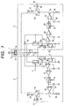
- Fig. 1 is a block diagram to explain a laser drive control circuit, which is an embodiment of the present invention.
- Reference symbol 1 designates a multi-beam laser, 1a a laser diode 1 (LD1), 1b a laser diode 2 (LD2), and 1c a photodiode (PD) for monitoring amounts of light from LD1 and LD2.
- this circuit has an LD1 drive control circuit 2 and an LD2 drive control circuit 3 and is comprised of an initial adjusting resistor Rm1 5 and a fixed resistor Rms 6 which are common to these drive control circuits.
- the initial adjusting resistor Rm1 5 is a resistor capable of being set variably at a desired resistance.
- monitor current 1 switches (SWs) 8a, 8b are selected to the LD1 drive control circuit 2 from a monitor current select signal 7.
- the switch 8b is connected in a switchable state between the fixed resistor Rms 6 and a final adjusting resistor Rm2 9.
- the monitor current (Im) 4 outputted from PD is converted to a monitor voltage (Vm) by the initial adjusting resistor Rm1 5, the LD2 final adjusting resistor Rm2 9, and the fixed resistor Rms 6.
- the initial adjusting resistor 5 and fixed resistor 6 are common resistors used for the adjustment operations of both LD1 and LD2.
- the monitor voltage is then sent to a control means having at least a gain amplifier (amplifying means) 10, a comparator (comparing means) 12, and a reference voltage generating means 11.
- the monitor voltage is amplified by the gain amplifier 10 and thereafter is inputted into the comparator 12 to be compared with the reference voltage a (Vref) of the reference voltage generator 11.
- Numeral 13 denotes a sample-hold circuit, which charges a hold capacitor 15 when the reference voltage a 11 is greater than the monitor voltage (Vm) in sampling according to a sample-hold signal 14, but discharges the hold capacitor 15 otherwise.
- the voltage appearing at the hold capacitor 15 is inputted into a drive amplifier 16 to cause the current set by a drive current setting resistor 18 to flow into the collector of a drive transistor 17.
- a switching transistor 19 When a switching transistor 19 is turned on by a laser modulation signal 21, it allows the current from the laser diode 1 of 1a to flow, thereby effecting emission of light. Since the operation of the LD2 drive control circuit 3 is similar to that of the LD1 drive control circuit 2 except that monitor current 2 switches (SWs) 25a, 25b are selected to the LD2 drive control circuit 3 from the monitor current select signal 7, the description thereof is omitted herein.
- SWs monitor current 2 switches
- numeral 24 represents an inverter, 25 monitor current 2 switches (SWs), 26 an LD2 final adjusting resistor Rm2', 27 a gain amplifier b, 28 a reference voltage b, 29 a comparator b, 30 a sample-hold circuit b, 31 a sample-hold signal b, 32 a sample-hold capacitor b, 33 a drive amplifier b, 34 a drive transistor b, 35 a drive current setting resistor b, 36 a switching transistor b, 37 a load resistor drive transistor b, 38 a laser modulation signal b, 39 a differential driver b, and 40 a laser load resistor.
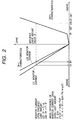
- Fig. 2 is a graph to show the laser drive current lop-emitted light amount L characteristics and the monitor current Im-emitted light amount L characteristics.
- the graph to show the Iop-L characteristics is illustrated on the right side of the axis of L [mW] indicating the emitted light amount L, and the graph to show the Im-L characteristics on the left side of the axis of L [mW].
- the relations of current values Iop, Im to emitted light amount L can be approximated each to a linear function.
- a total set resistance (Rm, Rm') of the adjusting resistors for each of the laser diode 1 and the laser diode 2 is determined uniquely from the reference voltage value Vref and each monitor current value (Im or Im').
- LD1 total set resistance Rm Rm1 + Rm2 + Rms
- LD2 total set resistance Rm' Rm1 + Rm2' + Rms
- maximums are set for the total set resistances of the adjusting resistors. These maximums need to be set so as to be not less than the resistance at the minimum specified light amount.
- Immax, Im'max represent the monitor currents at the maximum specified light amount.
- Fig. 3 is a flowchart to show the adjusting method. The method will be described herein with an example of the adjusting method using LD1 for the initial adjustment.
- the LD1 monitor current Im is selected by the monitor current switch SW (S1).
- the initial adjustment is started to adjust the initial adjusting resistor Rm1 into the specified range; if it is off the specified range it will be adjusted so as to be within the specified range (S2, S3).
- the adjustment is focused into the final specified range by the LD1 final adjusting resistor Rm2; if the resistance is off the final specified range the resistance will be adjusted into the final specified range (S4, S5).
- the monitor current switches (SWs) are turned to the LD2 side (S6). Since the initial adjustment has already been completed in the steps S2, S3 and can be omitted herein, the final adjustment of LD2 is carried out by the LD2 final adjusting resistor Rm2', thereby completing the adjustment (S7, S8).
- Fig. 4 is a graph to show the relationship between angle step and resistance.
- variable resistors of a rotating type which rotate in steps of equal angles, are used as the adjusting resistors.
- an effective rotation angle (full rotation angle) capable of outputting a resistance is represented by ⁇ and a rotation angle upon the initial adjustment (initial adjustment rotation angle) and a rotation angle upon the final adjustment (final adjustment rotation angle) by ⁇ int and ⁇ end, respectively.
- a moving angle in each adjustment will be called an angle step.
- Each adjusting resistor can be varied stepwise by an equal amount both upon the initial adjustment and upon the final adjustment.
- Angle steps during the respective adjustments will be called an initial angle step ⁇ S1 and a final angle step ⁇ S2.
- Initial angle step ⁇ S1 ⁇ int/ ⁇
- Final angle step ⁇ S2 ⁇ end/ ⁇
- the initial angle step may be set greater than the final angle step.
- the steps may be set so as to satisfy ⁇ S1 > ⁇ S2.
- a resistance resolution ⁇ RmINT in the initial adjustment (i.e., a change amount of resistance per single angular change) can be expressed as follows from the set maximum Rm1max of the initial adjusting resistor and the initial angle step ⁇ S1.
- ⁇ RmINT Rm1max ⁇ S1
- the resistance resolution ⁇ RmEND in the final adjustment of LD1 is expressed as follows from the total resistance Rm2max of the final adjusting resistor and the final angle step ⁇ S2.
- ⁇ RmEND Rm2max ⁇ S2
- Fig. 6 is a diagram to show the sectional structure of an image recording apparatus as an embodiment of the present invention and the structure of a density control device installed therein.
- numeral 61 denotes a color image-forming unit of the electrophotographic method
- 62 a photosensitive drum onto which laser beams are guided to form a latent image
- 63 a transfer drum for transferring an image developed from the latent image onto a recording sheet.
- Numeral 64 designates a laser scanning unit for emitting the laser light indicating an image signal.
- Numeral 60 represents a light source unit for emitting multiple beams, described previously, which has at least the laser diodes 1, 2, the photodiode (PD), the LD1 drive control circuit 2, and the LD2 drive control circuit 3 illustrated in Fig. 1.
- Numeral 70 denotes a polygon mirror and 71 a reflecting mirror. The light source unit 60 may also be set in the laser scanning unit 64.
- Numeral 65 indicates a developing unit for yellow toner which develops a yellow latent image
- 66 a developing unit for cyan toner
- 67 a developing unit for magenta toner
- 68 a developing unit for black toner
- Numeral 69 stands for a density sensor unit for detecting the density of an image formed on the photosensitive drum 62
- 610 for a detecting circuit for detecting a density sensor signal from the density sensor unit 69
- 611 for a reference voltage circuit for supplying the reference voltage to the signal detecting circuit 610.
- Numeral 612 designates a CPU (central processing unit) for executing the control of the whole of this apparatus.
- numeral 613 represents a development bias power supply for the yellow developing unit 65, 614 a development bias power supply for the cyan developing unit 66, 615 a development bias power supply for the magenta developing unit 67, and 616 a development bias power supply for the black developing unit 68.
- the sensitive drum 62 After charged by a charging unit not illustrated, is exposed to the laser light beams emitted form the laser diodes 1 and 2 and projected from the laser scanning unit 64.
- the multi-laser beams from the laser scanning unit 64 form a latent image on the surface of the photosensitive drum 62.
- the light amounts of the respective multi-laser beams are approximately equal.
- the yellow development bias power supply 613 is actuated to apply the development bias to the yellow developing unit 65 to visualize the yellow latent image with toner.
- the toner image thus visualized is attracted by transfer high-voltage power applied to the transfer drum 63, whereby it is transferred from the photosensitive drum 62 onto the transfer drum 63.
- the above sequential operation is carried out similarly for each of the colors (yellow Y, magenta M, cyan C, and black Bk), whereby a color image is formed on the transfer drum 63. After that, the color image is transferred onto a transfer sheet (not illustrated) and is then fixed to be printed out.
- the print sequences of the respective colors are independent of each other in the image recording apparatus, so that the toner densities of the respective colors can be detected by measuring the image on the photosensitive drum 62 or on the transfer drum 63 by the density sensor 69. Then toner compounding capable of achieving the optimum image quality can be implemented by controlling the recording condition (the bias herein) in each of the recording processes, using this detection result.
- the toner image transferred onto the photosensitive drum 62 is measured by a reflected light amount measuring system including the density sensor 69 and densities of the respective color toners are always combined stably.
- the present invention presents the effects of work saving of the adjusting circuits and reduction of the adjustment time in the drive control circuits of the multi-beam laser.
- the number of laser beams needs to be increased, for example to 4, in order to further enhance the quality of image, and the effects of work saving and reduction of the adjustment time become further outstanding in such cases.
Abstract
Description
- The present invention relates to a multi-laser driving apparatus and an adjusting method thereof and further to an image-forming apparatus having the multi-laser driving apparatus.
- A laser driving control method in the image-forming apparatus using multiple lasers is a feedback method of monitoring amounts of light emitted from laser diodes, from current values of a photodiode and, if necessary, properly adjusting driving currents of the laser diodes with reference to the light amounts.
- In this method, adjustment is necessary for uniformizing relations of amounts of the light emitted from the laser diodes to the monitor currents of the photodiode. In the multiple lasers, the monitor currents have delicate difference or variation between the laser diodes, and thus an independent adjusting circuit is given to each of the laser diodes to carry out an adjustment operation individually.
- Fig. 7 is a block diagram to explain a laser driving control circuit according to a prior art example.
- Reference symbol 1 designates a multi-beam laser, 1a a laser diode 1 (LD1), 1b a laser diode 2 (LD2), and 1c a photodiode (PD) for monitoring amounts of light from LD1 and LD2. In order to control the multi-beam laser 1, this circuit is comprised of LD1
drive control circuit 51 and LD2drive control circuit 52. - The operation of the LD1
drive control circuit 51 will be described schematically. In adjustment of LD1, monitor current 1 switch (SW) 8a andinitial adjusting resistor 102 are selected to the LD1drive control circuit 51 from a monitor currentselect signal 7. The monitor current (Im) outputted from PD passes through aline 4 to be converted to a monitor voltage (Vm) by the initial adjustingresistor 102, LD2 final adjustingresistor 9, and fixedresistor 101. The monitor voltage is amplified bygain amplifier 10 and thereafter is inputted into acomparator 12 to be compared with the reference voltage a of 11. Numeral 13 denotes a sample-hold circuit, which charges ahold capacitor 15 when the reference voltage a 11 is greater than the monitor voltage (Vm) in sampling according to a sample-hold signal 14, but discharges thehold capacitor 15 otherwise. The voltage appearing at thehold capacitor 15 is inputted into adrive amplifier 16 to cause a current set by drivecurrent setting resistor 18 to flow into the collector of drive transistor 17. When aswitching transistor 19 is turned on by alaser modulation signal 21, it allows the current from the laser diode 1 of 1a to flow to bring about emission of light. The operation of the LD2drive control circuit 3 is similar to that of the LD1 drive control circuit 2, and thus description thereof is omitted herein. - In the prior art example described above, the adjustment operation for the multi-beam laser is multiple; for example, in the case of a two-beam laser, the adjustment operation is double that of a single laser. In other words, the adjustment operation has to be carried out for each of single lasers.
- Namely, in the case of the structure of the above prior art example, the adjustment had to be carried out in such a manner that for the laser diode 1 the initial adjusting
resistor 102 was first adjusted and the final adjustingresistor 9 was adjusted thereafter and that for the laser diode 2 the initial adjustingresistor 105 was first adjusted and the final adjustingresistor 26 was adjusted thereafter. - The present invention has been accomplished in order to solve the above problem and an object of the present invention is to provide a multi-laser driving apparatus and an adjusting method thereof capable of saving the load of the adjusting step, or an image-forming apparatus having such a multi-laser driving apparatus.
- A multi-laser driving apparatus according to the present invention is a laser driving apparatus comprising:
- a plurality of laser emitting elements;
- a light receiving element for monitoring amounts of light from said laser emitting elements;
- current-voltage converting means for converting a light amount monitor current outputted from said light receiving element to a light amount monitor voltage; and
- control means for controlling a drive current of
each of said plurality of laser emitting elements,
based on said light amount monitor voltage outputted
from said current-voltage converting means,
wherein said current-voltage converting means comprises a common resistor and a plurality of non-common resistors, said common resistor being connected to said light receiving element and to each of said plurality of non-common resistors, and
wherein each of said non-common resistors is connected to said common resistor through switching means and connected to said control means. -
- A driving method according to the present invention is a laser driving method in which a light receiving element receives light from a laser emitting element, current-voltage converting means converts a monitor current outputted from the light receiving element to a monitor voltage, and control means controls a drive current of the laser emitting element, based on said monitor voltage,
wherein said current-voltage converting means comprises a common resistor and a non-common resistor and said common resistor together with said non-common resistor, is used for converting said monitor current corresponding to emission of light from each of a plurality of said laser emitting elements, to said monitor voltage, and
wherein the non-common resistor together with said common resistor converts said monitor current of a laser emitting element selected from said plurality of laser emitting elements, to said monitor voltage. - An image-forming apparatus according to the present invention comprises the laser driving apparatus described above.
-
- Fig. 1 is a block diagram of a laser driving circuit in an embodiment of the present invention;
- Fig. 2 is a graph to show laser driving current versus emission characteristics and monitor current versus emitted light amount characteristics in the embodiment of the present invention;
- Fig. 3 is a flowchart to show an adjusting method of the laser driving circuit in the embodiment of the present invention;
- Fig. 4 is a first graph to illustrate the adjustment process of the laser driving circuit in the embodiment of the present invention;
- Fig. 5 is a second graph to illustrate the adjustment process of the laser driving circuit in the embodiment of the present invention;
- Fig. 6 is a schematic diagram to show an image-forming apparatus of the present invention; and
- Fig. 7 is a block diagram of the laser driving circuit according to the prior art example.
-
- Fig. 1 is a block diagram to explain a laser drive control circuit, which is an embodiment of the present invention.
- Reference symbol 1 designates a multi-beam laser, 1a a laser diode 1 (LD1), 1b a laser diode 2 (LD2), and 1c a photodiode (PD) for monitoring amounts of light from LD1 and LD2. For controlling the multi-beam laser 1, this circuit has an LD1 drive control circuit 2 and an LD2
drive control circuit 3 and is comprised of an initial adjustingresistor Rm1 5 and afixed resistor Rms 6 which are common to these drive control circuits. The initial adjustingresistor Rm1 5 is a resistor capable of being set variably at a desired resistance. - The operation of the LD1 drive control circuit 2 will be described schematically. In the adjustment of LD1, monitor current 1 switches (SWs) 8a, 8b are selected to the LD1 drive control circuit 2 from a monitor current
select signal 7. Theswitch 8b is connected in a switchable state between thefixed resistor Rms 6 and a final adjustingresistor Rm2 9. The monitor current (Im) 4 outputted from PD is converted to a monitor voltage (Vm) by the initial adjustingresistor Rm1 5, the LD2 final adjustingresistor Rm2 9, and thefixed resistor Rms 6. The initial adjustingresistor 5 andfixed resistor 6 are common resistors used for the adjustment operations of both LD1 and LD2. The monitor voltage is then sent to a control means having at least a gain amplifier (amplifying means) 10, a comparator (comparing means) 12, and a reference voltage generating means 11. The monitor voltage is amplified by thegain amplifier 10 and thereafter is inputted into thecomparator 12 to be compared with the reference voltage a (Vref) of the reference voltage generator 11. Numeral 13 denotes a sample-hold circuit, which charges ahold capacitor 15 when the reference voltage a 11 is greater than the monitor voltage (Vm) in sampling according to a sample-hold signal 14, but discharges thehold capacitor 15 otherwise. The voltage appearing at thehold capacitor 15 is inputted into adrive amplifier 16 to cause the current set by a drivecurrent setting resistor 18 to flow into the collector of a drive transistor 17. When aswitching transistor 19 is turned on by alaser modulation signal 21, it allows the current from the laser diode 1 of 1a to flow, thereby effecting emission of light. Since the operation of the LD2drive control circuit 3 is similar to that of the LD1 drive control circuit 2 except that monitor current 2 switches (SWs) 25a, 25b are selected to the LD2drive control circuit 3 from the monitor currentselect signal 7, the description thereof is omitted herein. - In Fig. 1,
numeral 24 represents an inverter, 25 monitor current 2 switches (SWs), 26 an LD2 final adjusting resistor Rm2', 27 a gain amplifier b, 28 a reference voltage b, 29 a comparator b, 30 a sample-hold circuit b, 31 a sample-hold signal b, 32 a sample-hold capacitor b, 33 a drive amplifier b, 34 a drive transistor b, 35 a drive current setting resistor b, 36 a switching transistor b, 37 a load resistor drive transistor b, 38 a laser modulation signal b, 39 a differential driver b, and 40 a laser load resistor. - Fig. 2 is a graph to show the laser drive current lop-emitted light amount L characteristics and the monitor current Im-emitted light amount L characteristics. In the graph, the graph to show the Iop-L characteristics is illustrated on the right side of the axis of L [mW] indicating the emitted light amount L, and the graph to show the Im-L characteristics on the left side of the axis of L [mW]. The relations of current values Iop, Im to emitted light amount L can be approximated each to a linear function. Concerning the monitor current Im-emitted light amount L characteristics, there is delicate variation between the monitor currents for LD1 and LD2 at a given light amount, depending upon structures of the laser diodes, i.e., finish conditions of the individual laser diodes. In order to show the variation, two linear functions are graphed on the left side of the axis L [mW] in Fig. 2.
- Let us define a specified light amount value as P and suppose the following.
- Then the following relation holds.
- The prime mark "'" will be used hereinafter for expressing each of symbols related to LD2.
- Since the condition is that the feedback loop in the laser current control circuit at the specified light amount is in an equilibrium state, a total set resistance (Rm, Rm') of the adjusting resistors for each of the laser diode 1 and the laser diode 2 is determined uniquely from the reference voltage value Vref and each monitor current value (Im or Im').
- (In Eqs. (4) and (5) Rm1 and Rms are common and Rm2' is the final adjusting resistor concerning LD2.)
- Then the following equations hold.
- In the present invention we assume Rm1 > Rm2 and Rm1 > Rm2'.
- On the other hand, giving consideration to the fact that the specified light amount value has a certain width because of variation of optics etc., maximums (Rmmax, Rm'max) are set for the total set resistances of the adjusting resistors. These maximums need to be set so as to be not less than the resistance at the minimum specified light amount. Let the set maximums of the initial adjusting resistor Rm1 and the final adjusting resistors for LD1, LD2 be Rm1max, Rm2max, and Rm'2max and let the monitor currents at the minimum specified light amount be Immin and Im'min, respectively. Then the following relations hold.
- Likewise, consideration is also given to conditions upon maximum specified emission. Then minimums (Rmmin, Rm'min) are also set for the total set resistances of the adjusting resistors upon the maximum specified emission. These minimums are expressed by the following equations. Supposing these minimums are the fixed resistance Rms, the following relations are derived from the above argument.
- Here Immax, Im'max represent the monitor currents at the maximum specified light amount.
- Since the fixed resistance Rms is common, the following relation can be derived.
- However, since the initial adjusting resistor Rm1 is common, there occurs a difference ΔR between the resistance after the initial adjustment and each total set resistance (Rm, Rm'). Since the final adjusting resistors (Rm2, Rm2') need to be set at a value enough to absorb the variation of each monitor current, the following equations have to be satisfied.
- From the above argument, the setting conditions of the adjusting resistors are as follows.
- Fig. 3 is a flowchart to show the adjusting method. The method will be described herein with an example of the adjusting method using LD1 for the initial adjustment. First, the LD1 monitor current Im is selected by the monitor current switch SW (S1). Then the initial adjustment is started to adjust the initial adjusting resistor Rm1 into the specified range; if it is off the specified range it will be adjusted so as to be within the specified range (S2, S3). Then the adjustment is focused into the final specified range by the LD1 final adjusting resistor Rm2; if the resistance is off the final specified range the resistance will be adjusted into the final specified range (S4, S5). Then the monitor current switches (SWs) are turned to the LD2 side (S6). Since the initial adjustment has already been completed in the steps S2, S3 and can be omitted herein, the final adjustment of LD2 is carried out by the LD2 final adjusting resistor Rm2', thereby completing the adjustment (S7, S8).
- Fig. 4 is a graph to show the relationship between angle step and resistance. In the present embodiment variable resistors of a rotating type, which rotate in steps of equal angles, are used as the adjusting resistors. In that case, an effective rotation angle (full rotation angle) capable of outputting a resistance is represented by and a rotation angle upon the initial adjustment (initial adjustment rotation angle) and a rotation angle upon the final adjustment (final adjustment rotation angle) by int and end, respectively. A moving angle in each adjustment will be called an angle step. Each adjusting resistor can be varied stepwise by an equal amount both upon the initial adjustment and upon the final adjustment. Angle steps during the respective adjustments will be called an initial angle step ΔS1 and a final angle step ΔS2.
- In the present invention the initial angle step may be set greater than the final angle step. In other words, the steps may be set so as to satisfy ΔS1 > ΔS2.
- A resistance resolution ΔRmINT in the initial adjustment (i.e., a change amount of resistance per single angular change) can be expressed as follows from the set maximum Rm1max of the initial adjusting resistor and the initial angle step ΔS1.
- For the adjustments, the adjusting method of gradually increasing the light amount is employed for the purpose of protecting the laser. Then the initial values of the adjusting resistors are started from the maximum. Fig. 5 is a graph to show the relationship between angle step and resistance in the final adjustment. As illustrated in Fig 5, supposing that the initial adjustment was achieved by the number steps Sn from the initial value of the set resistance into the specified range, the initial adjustment value Rt is given by
(Reference is made to Fig. 5.) - The resistance resolution ΔRmEND in the final adjustment of LD1 is expressed as follows from the total resistance Rm2max of the final adjusting resistor and the final angle step ΔS2.
- Supposing that the final adjustment of LD2 was achieved by the number of steps Sm into the specified range, the final adjustment value Rt is given by
- Fig. 6 is a diagram to show the sectional structure of an image recording apparatus as an embodiment of the present invention and the structure of a density control device installed therein.
- In Fig. 6, numeral 61 denotes a color image-forming unit of the electrophotographic method, 62 a photosensitive drum onto which laser beams are guided to form a latent image, and 63 a transfer drum for transferring an image developed from the latent image onto a recording sheet.
Numeral 64 designates a laser scanning unit for emitting the laser light indicating an image signal.Numeral 60 represents a light source unit for emitting multiple beams, described previously, which has at least the laser diodes 1, 2, the photodiode (PD), the LD1 drive control circuit 2, and the LD2drive control circuit 3 illustrated in Fig. 1.Numeral 70 denotes a polygon mirror and 71 a reflecting mirror. Thelight source unit 60 may also be set in thelaser scanning unit 64. -
Numeral 65 indicates a developing unit for yellow toner which develops a yellow latent image, 66 a developing unit for cyan toner, 67 a developing unit for magenta toner, and 68 a developing unit for black toner.Numeral 69 stands for a density sensor unit for detecting the density of an image formed on thephotosensitive drum density sensor unit signal detecting circuit 610.Numeral 612 designates a CPU (central processing unit) for executing the control of the whole of this apparatus. - Further, numeral 613 represents a development bias power supply for the yellow developing
unit 65, 614 a development bias power supply for thecyan developing unit 66, 615 a development bias power supply for themagenta developing unit 67, and 616 a development bias power supply for the black developingunit 68. - Described next is the operation of the image recording apparatus having the above structure.
- At the color image-forming
unit 61, thesensitive drum 62, after charged by a charging unit not illustrated, is exposed to the laser light beams emitted form the laser diodes 1 and 2 and projected from thelaser scanning unit 64. The multi-laser beams from thelaser scanning unit 64 form a latent image on the surface of thephotosensitive drum 62. The light amounts of the respective multi-laser beams are approximately equal. For example, after formation of the yellow latent image, the yellow developmentbias power supply 613 is actuated to apply the development bias to the yellow developingunit 65 to visualize the yellow latent image with toner. The toner image thus visualized is attracted by transfer high-voltage power applied to thetransfer drum 63, whereby it is transferred from thephotosensitive drum 62 onto thetransfer drum 63. - The above sequential operation is carried out similarly for each of the colors (yellow Y, magenta M, cyan C, and black Bk), whereby a color image is formed on the
transfer drum 63. After that, the color image is transferred onto a transfer sheet (not illustrated) and is then fixed to be printed out. - As apparent from the above series of print sequences, the print sequences of the respective colors are independent of each other in the image recording apparatus, so that the toner densities of the respective colors can be detected by measuring the image on the
photosensitive drum 62 or on thetransfer drum 63 by thedensity sensor 69. Then toner compounding capable of achieving the optimum image quality can be implemented by controlling the recording condition (the bias herein) in each of the recording processes, using this detection result. - In the present embodiment, therefore, the toner image transferred onto the
photosensitive drum 62 is measured by a reflected light amount measuring system including thedensity sensor 69 and densities of the respective color toners are always combined stably. - As described above, the present invention presents the effects of work saving of the adjusting circuits and reduction of the adjustment time in the drive control circuits of the multi-beam laser. There are cases wherein the number of laser beams needs to be increased, for example to 4, in order to further enhance the quality of image, and the effects of work saving and reduction of the adjustment time become further outstanding in such cases.
Claims (11)
- A laser driving apparatus comprising:a plurality of laser emitting elements;a light receiving element for monitoring amounts of light from said laser emitting elements;current-voltage converting means for converting a light amount monitor current outputted from said light receiving element to a light amount monitor voltage; andcontrol means for controlling a drive current of each of said plurality of laser emitting elements, based on said light amount monitor voltage outputted from said current-voltage converting means,
wherein said current-voltage converting means comprises a common resistor and a plurality of non-common resistors, said common resistor being connected to said light receiving element and to each of said plurality of non-common resistors, and
wherein each of said non-common resistors is connected to said common resistor through switching means and connected to said control means. - The laser driving apparatus according to Claim 1, wherein said light receiving element is one light receiving element.
- The laser driving apparatus according to Claim 1, wherein said control means comprises amplifying means for amplifying the light amount monitor voltage, reference voltage generating means for generating a reference voltage, and comparing means for comparing an output signal of said amplifying means with an output signal of said reference voltage generating means.
- The laser driving apparatus according to Claim 3, wherein at least one of said amplifying means, said reference voltage generating means, and said comparing means is arranged so as to permit common control of the drive currents of said plurality of laser emitting elements.
- The laser driving apparatus according to Claim 3, wherein said control means further comprises signal holding means for sampling and holding an output signal of said comparing means, based on a sample-hold control signal, current generating means for generating a current according to a signal held by said signal holding means, and modulating means for modulating the current generated by said current generating means, to a modulation current modulated based on an external video signal.
- The laser driving apparatus according to Claim 1, wherein said common resistor comprises variable means for making a current-voltage conversion rate variable.
- The laser driving apparatus according to Claim 1, wherein each of said non-common resistors comprises variable means for making a current-voltage conversion rate variable.
- An image-forming apparatus comprising the laser driving apparatus as set forth in Claim 1.
- A laser driving method in which a light receiving element receives light from a laser emitting element, current-voltage converting means converts a monitor current outputted from the light receiving element to a monitor voltage, and control means controls a drive current of the laser emitting element, based on said monitor voltage,
wherein said current-voltage converting means comprises a common resistor and a non-common resistor and said common resistor together with said non-common resistor, is used for converting said monitor current corresponding to emission of light from each of a plurality of said laser emitting elements, to said monitor voltage, and
wherein the non-common resistor together with said common resistor converts said monitor current of a laser emitting element selected from said plurality of laser emitting elements, to said monitor voltage. - A multi-laser driving apparatus comprising a laser device, said laser device comprising a plurality of laser diodes for emitting laser light and a single photodiode for monitoring an amount of light from each of said plurality of laser diodes to output a light amount monitor current according to the amount of light; a plurality of current-voltage converting means, corresponding to the respective laser diodes, for converting said light amount monitor current to a light amount monitor voltage; and a plurality of control means for controlling a drive current of each of said plurality of laser diodes according to the light amount monitor voltage outputted from each of said current-voltage converting means,
wherein each of said plurality of control means comprises amplifying means for amplifying said light amount monitor voltage, reference voltage generating means for generating a reference voltage, comparing means for comparing an output signal of said amplifying means with an output signal of said reference voltage generating means, signal holding means for sampling and holding an output signal of said comparing means, based on a sample-hold control signal, current generating means for generating a current according to the signal held by said signal holding means, and modulating means for modulating the current generated by said current generating means, to a modulation current modulated based on an external video signal,
wherein said modulation current generated in each of said plurality of control means is used as said drive current of each laser diode,
wherein said plurality of current-voltage converting means share one common portion, and wherein a non-common portion and said common portion of said plurality of current-voltage converting means comprise variable means for making a current-voltage conversion rate variable. - An adjusting method for adjusting the multi-laser driving apparatus as set forth in Claim 10, wherein the variable means of said non-common portion is adjusted after the variable means of said common portion has been adjusted.
Applications Claiming Priority (4)
| Application Number | Priority Date | Filing Date | Title |
|---|---|---|---|
| JP33445698 | 1998-11-25 | ||
| JP33445698 | 1998-11-25 | ||
| JP32828199 | 1999-11-18 | ||
| JP11328281A JP2000218865A (en) | 1998-11-25 | 1999-11-18 | Laser-driving apparatus, its drive method and image- forming apparatus using the same |
Publications (3)
| Publication Number | Publication Date |
|---|---|
| EP1005121A2 true EP1005121A2 (en) | 2000-05-31 |
| EP1005121A3 EP1005121A3 (en) | 2002-10-16 |
| EP1005121B1 EP1005121B1 (en) | 2004-10-06 |
Family
ID=26572811
Family Applications (1)
| Application Number | Title | Priority Date | Filing Date |
|---|---|---|---|
| EP99123349A Expired - Lifetime EP1005121B1 (en) | 1998-11-25 | 1999-11-23 | Laser driving apparatus, driving method thereof, and image-forming apparatus using it |
Country Status (4)
| Country | Link |
|---|---|
| US (1) | US6560256B1 (en) |
| EP (1) | EP1005121B1 (en) |
| JP (1) | JP2000218865A (en) |
| DE (1) | DE69920850T2 (en) |
Cited By (2)
| Publication number | Priority date | Publication date | Assignee | Title |
|---|---|---|---|---|
| WO2004003900A1 (en) * | 2002-06-28 | 2004-01-08 | Thomson Licensing S.A. | Intrinsically safe pick-up for reproduction or recording devices for different optical recording media |
| CN108572526A (en) * | 2017-03-08 | 2018-09-25 | 株式会社东芝 | Light-emitting substrate, print head and image forming apparatus |
Families Citing this family (18)
| Publication number | Priority date | Publication date | Assignee | Title |
|---|---|---|---|---|
| US6330324B1 (en) * | 1997-12-09 | 2001-12-11 | Sbc Technology Resources, Inc. | Geographical call routing for a non-emergency calling service |
| JP2001244555A (en) * | 2000-03-01 | 2001-09-07 | Pioneer Electronic Corp | Automatic power control circuit |
| US6801556B2 (en) * | 2001-11-09 | 2004-10-05 | Agere Systems Inc. | Optical source driver with output load detection circuit |
| US7022960B2 (en) * | 2002-02-12 | 2006-04-04 | Konica Corporation | Photographic film image reading apparatus with film density detection |
| JP2004103839A (en) * | 2002-09-10 | 2004-04-02 | Canon Inc | Semiconductor multiple beam laser device and image forming device |
| EP1455520A3 (en) | 2003-03-03 | 2005-10-05 | Canon Kabushiki Kaisha | Frequency modulation apparatus and frequency modulation method |
| JP4308812B2 (en) * | 2005-10-28 | 2009-08-05 | 日本テキサス・インスツルメンツ株式会社 | Light emitting element driving device |
| JP4214490B2 (en) * | 2006-08-29 | 2009-01-28 | ブラザー工業株式会社 | Laser light output control device and image forming apparatus |
| US7891570B2 (en) * | 2007-02-28 | 2011-02-22 | Microvision, Inc. | Photodiode with improved performance in ambient light |
| TWI367692B (en) * | 2007-09-21 | 2012-07-01 | Aussmak Optoelectronic Corp | Light emitting device and control method thereof |
| US20110080533A1 (en) * | 2009-10-06 | 2011-04-07 | Microvision, Inc. | Dithering Laser Drive Apparatus |
| WO2011156951A1 (en) * | 2010-06-13 | 2011-12-22 | Mediatek Singapore Pte. Ltd. | Method for reducing a number of input terminals of an automatic power control circuit, and associated automatic power control circuit |
| JP5818495B2 (en) | 2011-04-21 | 2015-11-18 | キヤノン株式会社 | Image forming apparatus |
| JP6178641B2 (en) | 2013-06-28 | 2017-08-09 | キヤノン株式会社 | Optical scanning apparatus and image forming apparatus |
| US10496004B2 (en) | 2015-08-20 | 2019-12-03 | Canon Kabushiki Kaisha | Image forming apparatus with current-controlled light emitting element |
| JP6609144B2 (en) | 2015-09-10 | 2019-11-20 | キヤノン株式会社 | Optical scanning device |
| JP6671931B2 (en) | 2015-11-16 | 2020-03-25 | キヤノン株式会社 | Image forming device |
| JP2017219714A (en) | 2016-06-08 | 2017-12-14 | キヤノン株式会社 | Optical scanner |
Citations (8)
| Publication number | Priority date | Publication date | Assignee | Title |
|---|---|---|---|---|
| JPS56140477A (en) * | 1980-04-02 | 1981-11-02 | Ricoh Co Ltd | Laser driving control system |
| JPS61224478A (en) * | 1985-03-29 | 1986-10-06 | Canon Inc | Laser driving equipment |
| JPS62227667A (en) * | 1986-03-31 | 1987-10-06 | Canon Inc | Laser drive controller |
| US4876442A (en) * | 1987-10-30 | 1989-10-24 | Nec Corporation | Laser control circuit |
| US4985896A (en) * | 1985-03-29 | 1991-01-15 | Canon Kabushiki Kaisha | Laser driving device |
| JPH0636329A (en) * | 1992-07-17 | 1994-02-10 | Matsushita Electric Ind Co Ltd | Laser array provided with power control circuit |
| JPH08116114A (en) * | 1994-10-17 | 1996-05-07 | Fuji Xerox Co Ltd | Quantity-of-light control apparatus |
| JPH10209545A (en) * | 1997-01-22 | 1998-08-07 | Fuji Xerox Co Ltd | Light quantity controller |
Family Cites Families (8)
| Publication number | Priority date | Publication date | Assignee | Title |
|---|---|---|---|---|
| JPS6446724A (en) | 1987-08-17 | 1989-02-21 | Canon Kk | Image recorder |
| DE69132464T2 (en) * | 1990-07-05 | 2001-05-10 | Canon Kk | Imaging device and associated switching device for constant current switching |
| US5504517A (en) | 1991-04-04 | 1996-04-02 | Canon Kabushiki Kaisha | Laser scanner control circuit which is used in image forming apparatus and driver IC for use in such a circuit |
| US5822343A (en) * | 1994-08-26 | 1998-10-13 | Psc Inc. | Operating and control system for lasers useful in bar code scanners |
| US5726437A (en) * | 1994-10-27 | 1998-03-10 | Fuji Xerox Co., Ltd. | Light intensity control device |
| JP4235275B2 (en) * | 1998-01-09 | 2009-03-11 | キヤノン株式会社 | Image forming apparatus |
| US6055252A (en) * | 1998-09-10 | 2000-04-25 | Photonic Solutions, Inc. | Fiberoptic transmitter using thermistor to maintain stable operating conditions over a range of temperature |
| JP4148485B2 (en) * | 1998-10-05 | 2008-09-10 | キヤノン株式会社 | Image forming apparatus and copying machine |
-
1999
- 1999-11-18 JP JP11328281A patent/JP2000218865A/en active Pending
- 1999-11-23 US US09/447,285 patent/US6560256B1/en not_active Expired - Lifetime
- 1999-11-23 DE DE69920850T patent/DE69920850T2/en not_active Expired - Lifetime
- 1999-11-23 EP EP99123349A patent/EP1005121B1/en not_active Expired - Lifetime
Patent Citations (8)
| Publication number | Priority date | Publication date | Assignee | Title |
|---|---|---|---|---|
| JPS56140477A (en) * | 1980-04-02 | 1981-11-02 | Ricoh Co Ltd | Laser driving control system |
| JPS61224478A (en) * | 1985-03-29 | 1986-10-06 | Canon Inc | Laser driving equipment |
| US4985896A (en) * | 1985-03-29 | 1991-01-15 | Canon Kabushiki Kaisha | Laser driving device |
| JPS62227667A (en) * | 1986-03-31 | 1987-10-06 | Canon Inc | Laser drive controller |
| US4876442A (en) * | 1987-10-30 | 1989-10-24 | Nec Corporation | Laser control circuit |
| JPH0636329A (en) * | 1992-07-17 | 1994-02-10 | Matsushita Electric Ind Co Ltd | Laser array provided with power control circuit |
| JPH08116114A (en) * | 1994-10-17 | 1996-05-07 | Fuji Xerox Co Ltd | Quantity-of-light control apparatus |
| JPH10209545A (en) * | 1997-01-22 | 1998-08-07 | Fuji Xerox Co Ltd | Light quantity controller |
Non-Patent Citations (6)
| Title |
|---|
| PATENT ABSTRACTS OF JAPAN vol. 006, no. 018 (P-100), 2 February 1982 (1982-02-02) -& JP 56 140477 A (RICOH CO LTD), 2 November 1981 (1981-11-02) * |
| PATENT ABSTRACTS OF JAPAN vol. 011, no. 065 (E-484), 27 February 1987 (1987-02-27) -& JP 61 224478 A (CANON INC), 6 October 1986 (1986-10-06) * |
| PATENT ABSTRACTS OF JAPAN vol. 012, no. 087 (M-678), 19 March 1988 (1988-03-19) -& JP 62 227667 A (CANON INC), 6 October 1987 (1987-10-06) * |
| PATENT ABSTRACTS OF JAPAN vol. 018, no. 264 (P-1740), 19 May 1994 (1994-05-19) -& JP 06 036329 A (MATSUSHITA ELECTRIC IND CO LTD), 10 February 1994 (1994-02-10) * |
| PATENT ABSTRACTS OF JAPAN vol. 1996, no. 09, 30 September 1996 (1996-09-30) -& JP 08 116114 A (FUJI XEROX CO LTD), 7 May 1996 (1996-05-07) * |
| PATENT ABSTRACTS OF JAPAN vol. 1998, no. 13, 30 November 1998 (1998-11-30) -& JP 10 209545 A (FUJI XEROX CO LTD), 7 August 1998 (1998-08-07) * |
Cited By (2)
| Publication number | Priority date | Publication date | Assignee | Title |
|---|---|---|---|---|
| WO2004003900A1 (en) * | 2002-06-28 | 2004-01-08 | Thomson Licensing S.A. | Intrinsically safe pick-up for reproduction or recording devices for different optical recording media |
| CN108572526A (en) * | 2017-03-08 | 2018-09-25 | 株式会社东芝 | Light-emitting substrate, print head and image forming apparatus |
Also Published As
| Publication number | Publication date |
|---|---|
| EP1005121B1 (en) | 2004-10-06 |
| DE69920850T2 (en) | 2005-02-10 |
| EP1005121A3 (en) | 2002-10-16 |
| US6560256B1 (en) | 2003-05-06 |
| JP2000218865A (en) | 2000-08-08 |
| DE69920850D1 (en) | 2004-11-11 |
Similar Documents
| Publication | Publication Date | Title |
|---|---|---|
| EP1005121B1 (en) | Laser driving apparatus, driving method thereof, and image-forming apparatus using it | |
| US5966395A (en) | Semiconductor laser drive device and image recording device | |
| US7643525B2 (en) | Current driver and power control for electrophotographic devices | |
| US4796265A (en) | Imaging using collectively controlled multiple beams | |
| US6324197B1 (en) | Power controller for semiconductor laser device | |
| US5504517A (en) | Laser scanner control circuit which is used in image forming apparatus and driver IC for use in such a circuit | |
| US4771431A (en) | Semiconductor laser drive | |
| JPS62124576A (en) | Output adjusting device for semiconductor laser | |
| US5832012A (en) | Laser scanning unit having automatic power control function | |
| US6989520B2 (en) | Emission control apparatus with settable target intensity and image forming apparatus using same | |
| US5973719A (en) | Laser scanning unit having automatic power control function | |
| US9964887B2 (en) | Light scanning apparatus and image forming apparatus | |
| JP2007158022A (en) | Semiconductor laser driver circuit | |
| US5859659A (en) | Laser beam scanning device and method including light intensity adjustment | |
| JP4356958B2 (en) | Image forming apparatus and laser drive control method in the apparatus | |
| US5126761A (en) | Scanning beam output control device for an image recorder | |
| US4929970A (en) | Laser printer | |
| US6574447B2 (en) | Laser beam emission control for electrophotographic device | |
| JP2000187374A (en) | Image forming device | |
| JP2004009492A (en) | Laser driving circuit in image formation device | |
| US5450118A (en) | Image forming apparatus | |
| US7403215B2 (en) | Current driver and power control for electrophotographic devices | |
| JP2000238331A (en) | Light source-driving apparatus and image-forming apparatus | |
| EP0841598A2 (en) | Laser light amount control device and image recording apparatus using the device | |
| KR100247985B1 (en) | Laser scanning system of printer |
Legal Events
| Date | Code | Title | Description |
|---|---|---|---|
| PUAI | Public reference made under article 153(3) epc to a published international application that has entered the european phase |
Free format text: ORIGINAL CODE: 0009012 |
|
| AK | Designated contracting states |
Kind code of ref document: A2 Designated state(s): AT BE CH CY DE DK ES FI FR GB GR IE IT LI LU MC NL PT SE |
|
| AX | Request for extension of the european patent |
Free format text: AL;LT;LV;MK;RO;SI |
|
| PUAL | Search report despatched |
Free format text: ORIGINAL CODE: 0009013 |
|
| AK | Designated contracting states |
Kind code of ref document: A3 Designated state(s): AT BE CH CY DE DK ES FI FR GB GR IE IT LI LU MC NL PT SE |
|
| AX | Request for extension of the european patent |
Free format text: AL;LT;LV;MK;RO;SI |
|
| RIC1 | Information provided on ipc code assigned before grant |
Free format text: 7H 01S 5/042 A, 7H 01S 5/0683 B, 7H 04N 1/00 B, 7H 01S 5/40 B |
|
| 17P | Request for examination filed |
Effective date: 20030228 |
|
| 17Q | First examination report despatched |
Effective date: 20030410 |
|
| AKX | Designation fees paid |
Designated state(s): DE FR GB IT |
|
| GRAP | Despatch of communication of intention to grant a patent |
Free format text: ORIGINAL CODE: EPIDOSNIGR1 |
|
| GRAS | Grant fee paid |
Free format text: ORIGINAL CODE: EPIDOSNIGR3 |
|
| GRAA | (expected) grant |
Free format text: ORIGINAL CODE: 0009210 |
|
| AK | Designated contracting states |
Kind code of ref document: B1 Designated state(s): DE FR GB IT |
|
| PG25 | Lapsed in a contracting state [announced via postgrant information from national office to epo] |
Ref country code: IT Free format text: LAPSE BECAUSE OF FAILURE TO SUBMIT A TRANSLATION OF THE DESCRIPTION OR TO PAY THE FEE WITHIN THE PRESCRIBED TIME-LIMIT;WARNING: LAPSES OF ITALIAN PATENTS WITH EFFECTIVE DATE BEFORE 2007 MAY HAVE OCCURRED AT ANY TIME BEFORE 2007. THE CORRECT EFFECTIVE DATE MAY BE DIFFERENT FROM THE ONE RECORDED. Effective date: 20041006 Ref country code: FR Free format text: LAPSE BECAUSE OF NON-PAYMENT OF DUE FEES Effective date: 20041006 |
|
| REG | Reference to a national code |
Ref country code: GB Ref legal event code: FG4D |
|
| REG | Reference to a national code |
Ref country code: IE Ref legal event code: FG4D |
|
| REF | Corresponds to: |
Ref document number: 69920850 Country of ref document: DE Date of ref document: 20041111 Kind code of ref document: P |
|
| PLBE | No opposition filed within time limit |
Free format text: ORIGINAL CODE: 0009261 |
|
| STAA | Information on the status of an ep patent application or granted ep patent |
Free format text: STATUS: NO OPPOSITION FILED WITHIN TIME LIMIT |
|
| 26N | No opposition filed |
Effective date: 20050707 |
|
| EN | Fr: translation not filed | ||
| PGFP | Annual fee paid to national office [announced via postgrant information from national office to epo] |
Ref country code: GB Payment date: 20171130 Year of fee payment: 19 |
|
| PGFP | Annual fee paid to national office [announced via postgrant information from national office to epo] |
Ref country code: DE Payment date: 20180131 Year of fee payment: 19 |
|
| REG | Reference to a national code |
Ref country code: DE Ref legal event code: R119 Ref document number: 69920850 Country of ref document: DE |
|
| GBPC | Gb: european patent ceased through non-payment of renewal fee |
Effective date: 20181123 |
|
| PG25 | Lapsed in a contracting state [announced via postgrant information from national office to epo] |
Ref country code: DE Free format text: LAPSE BECAUSE OF NON-PAYMENT OF DUE FEES Effective date: 20190601 |
|
| PG25 | Lapsed in a contracting state [announced via postgrant information from national office to epo] |
Ref country code: GB Free format text: LAPSE BECAUSE OF NON-PAYMENT OF DUE FEES Effective date: 20181123 |