EP1011047B1 - Fault recovery method and storage controller in information processing apparatus - Google Patents
Fault recovery method and storage controller in information processing apparatus Download PDFInfo
- Publication number
- EP1011047B1 EP1011047B1 EP99117283A EP99117283A EP1011047B1 EP 1011047 B1 EP1011047 B1 EP 1011047B1 EP 99117283 A EP99117283 A EP 99117283A EP 99117283 A EP99117283 A EP 99117283A EP 1011047 B1 EP1011047 B1 EP 1011047B1
- Authority
- EP
- European Patent Office
- Prior art keywords
- access
- fault
- shared memory
- shared
- processors
- Prior art date
- Legal status (The legal status is an assumption and is not a legal conclusion. Google has not performed a legal analysis and makes no representation as to the accuracy of the status listed.)
- Expired - Lifetime
Links
Images


Classifications
-
- G—PHYSICS
- G06—COMPUTING; CALCULATING OR COUNTING
- G06F—ELECTRIC DIGITAL DATA PROCESSING
- G06F11/00—Error detection; Error correction; Monitoring
- G06F11/07—Responding to the occurrence of a fault, e.g. fault tolerance
- G06F11/16—Error detection or correction of the data by redundancy in hardware
- G06F11/20—Error detection or correction of the data by redundancy in hardware using active fault-masking, e.g. by switching out faulty elements or by switching in spare elements
- G06F11/2002—Error detection or correction of the data by redundancy in hardware using active fault-masking, e.g. by switching out faulty elements or by switching in spare elements where interconnections or communication control functionality are redundant
- G06F11/2007—Error detection or correction of the data by redundancy in hardware using active fault-masking, e.g. by switching out faulty elements or by switching in spare elements where interconnections or communication control functionality are redundant using redundant communication media
- G06F11/201—Error detection or correction of the data by redundancy in hardware using active fault-masking, e.g. by switching out faulty elements or by switching in spare elements where interconnections or communication control functionality are redundant using redundant communication media between storage system components
-
- G—PHYSICS
- G06—COMPUTING; CALCULATING OR COUNTING
- G06F—ELECTRIC DIGITAL DATA PROCESSING
- G06F11/00—Error detection; Error correction; Monitoring
- G06F11/07—Responding to the occurrence of a fault, e.g. fault tolerance
- G06F11/0703—Error or fault processing not based on redundancy, i.e. by taking additional measures to deal with the error or fault not making use of redundancy in operation, in hardware, or in data representation
- G06F11/0706—Error or fault processing not based on redundancy, i.e. by taking additional measures to deal with the error or fault not making use of redundancy in operation, in hardware, or in data representation the processing taking place on a specific hardware platform or in a specific software environment
- G06F11/0721—Error or fault processing not based on redundancy, i.e. by taking additional measures to deal with the error or fault not making use of redundancy in operation, in hardware, or in data representation the processing taking place on a specific hardware platform or in a specific software environment within a central processing unit [CPU]
- G06F11/0724—Error or fault processing not based on redundancy, i.e. by taking additional measures to deal with the error or fault not making use of redundancy in operation, in hardware, or in data representation the processing taking place on a specific hardware platform or in a specific software environment within a central processing unit [CPU] in a multiprocessor or a multi-core unit
-
- G—PHYSICS
- G06—COMPUTING; CALCULATING OR COUNTING
- G06F—ELECTRIC DIGITAL DATA PROCESSING
- G06F11/00—Error detection; Error correction; Monitoring
- G06F11/07—Responding to the occurrence of a fault, e.g. fault tolerance
- G06F11/0703—Error or fault processing not based on redundancy, i.e. by taking additional measures to deal with the error or fault not making use of redundancy in operation, in hardware, or in data representation
- G06F11/0706—Error or fault processing not based on redundancy, i.e. by taking additional measures to deal with the error or fault not making use of redundancy in operation, in hardware, or in data representation the processing taking place on a specific hardware platform or in a specific software environment
- G06F11/073—Error or fault processing not based on redundancy, i.e. by taking additional measures to deal with the error or fault not making use of redundancy in operation, in hardware, or in data representation the processing taking place on a specific hardware platform or in a specific software environment in a memory management context, e.g. virtual memory or cache management
-
- G—PHYSICS
- G06—COMPUTING; CALCULATING OR COUNTING
- G06F—ELECTRIC DIGITAL DATA PROCESSING
- G06F11/00—Error detection; Error correction; Monitoring
- G06F11/07—Responding to the occurrence of a fault, e.g. fault tolerance
- G06F11/0703—Error or fault processing not based on redundancy, i.e. by taking additional measures to deal with the error or fault not making use of redundancy in operation, in hardware, or in data representation
- G06F11/079—Root cause analysis, i.e. error or fault diagnosis
-
- G—PHYSICS
- G06—COMPUTING; CALCULATING OR COUNTING
- G06F—ELECTRIC DIGITAL DATA PROCESSING
- G06F11/00—Error detection; Error correction; Monitoring
- G06F11/07—Responding to the occurrence of a fault, e.g. fault tolerance
- G06F11/14—Error detection or correction of the data by redundancy in operation
- G06F11/1402—Saving, restoring, recovering or retrying
- G06F11/1405—Saving, restoring, recovering or retrying at machine instruction level
- G06F11/141—Saving, restoring, recovering or retrying at machine instruction level for bus or memory accesses
Definitions
- the present invention relates generally to a fault recovery method for a storage apparatus of a computer-based information processing system or a computer-based information processing apparatus and is associated with fault detection and fault recovery for ensuring the continuation of a desired operation of the system as a whole even if the storage apparatus, a component of the system, fails. More particularly, the present invention relates to a linking technology for linking a processor with a shared module in a multiprocessor system and a fault tolerance control technology based on the linking technology.
- Japanese Patent Laid-open No. Hei 9-160723 discloses a double bus connecting scheme, an extended version of the above-mentioned shared bus connecting scheme.
- This double bus connecting scheme requires a dedicated feature for shared-bus arbitration. In this scheme, if the shared bus itself fails or the bus arbitration feature fails, the entire system is disabled. To solve this problem, a connecting scheme has been proposed in which a plurality of shared buses is further prepared to provide redundancy.
- US-5 790 775 discloses a storage controller having the features recited in the precharacterising first part of claim 3 in common with the present invention.
- the storage controller of this prior art consists of two controllers each having access to the cache memory of the other. Each controller includes a-shared memory for use by its internal units. Both controllers exchange "keep alive" messages. A controller failing to receive the "keep alive” messages of the other, reports to the host computer that a fault has occurred in the other controller, destages the cache contents of the other controller to the disk devices and listens to commands addressed to the failed controller.
- An embodiment of the present invention provides, in an information processing apparatus having multiple processors, a method of connecting a plurality of individual paths capable of ensuring data integrity.
- a multiple individual path connecting method in which two or more connection paths are provided between each processor and each shared module in the system. If a fault is detected, tests are made by switching between the communication paths to totally judge a fault location.
- a system shared module such as a shared memory is arranged with an address locking unit to perform exclusive control in a predetermined address range. If a request for access requiring address exclusive control is made, the access address is registered to indicate that the address is in a locked state. When another access request is made to the locked address, the access address is compared with the locked address. If the access address is found matching the locked address, the access is held in a wait state until the address is unlocked and the access is made again after the address locking is cleared, thereby ensuring data integrity.
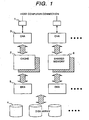
- the storage apparatus comprises a channel connection system 1 for connection to a host computer, not shown, which is a higher-level apparatus, a cache memory 2 for temporarily storing input/output data, a channel adapter (hereafter referred to as CHA) for controlling the data transfer between the channel connection system 1 and the cache memory 2, a disk array 4, which is a storage medium for storing data, a disk adapter (hereafter referred to as DKA) for controlling the data transfer between the cache memory 2 and the disk array 4, and a shared memory 6 provided between the CHA 3 and the DKA 5.
- the shared memory 6 will be detailed later.
- FIG. 1 is schematic and therefore does not illustrate detail connections.
- the cache memory 2 and the shared memory 6 are connected to one CHA or (DKA).
- DKA DKA
- the channel connection system includes, for example, a channel controller in the case of the connection with a mainframe-type host computer (CKD data format) and a SCSI bus controller in the case of the connection with a UNIX-type computer (FBA data format).
- CKD data format mainframe-type host computer
- FBA data format UNIX-type computer
- a controller based on fiber channel may be available.
- the shared memory 6 stores control information such as the directory information (a hierarchical table for cache segment search, and the state of each segment) for controlling the use of the cache memory 2, processor-to-processor communication messages (the contents of communication to be executed for the cooperation and synchronization between processors) between the CHA 3 and the DKA 5, system configuration information (the common information associated with the system configuration states such as the mounting states of the CHA 3 and the DKA 5 existing in the system, the storage sizes of the cache memory 2 and the shared memory 6, and the number of disk arrays 4).
- control information such as the directory information (a hierarchical table for cache segment search, and the state of each segment) for controlling the use of the cache memory 2, processor-to-processor communication messages (the contents of communication to be executed for the cooperation and synchronization between processors) between the CHA 3 and the DKA 5, system configuration information (the common information associated with the system configuration states such as the mounting states of the CHA 3 and the DKA 5 existing in the system, the storage sizes of the cache memory 2 and the shared memory 6, and the number of
- the CHA 3 receives a command from the host computer through the channel connection system 1, interprets the received command, and controls data transfer.
- the following describes the basic operation to be performed when the CHA 3 receives a read command for data for example from the host computer.
- the CHA 3 accesses the shared memory 6 to check the cache memory 2 for the data to be read. If the target data is found in the cache memory 2, the CHA 3 transfers this data to the host computer from the cache memory 2 through the channel connection system 1. If the target data is not found, the CHA 3 uses the shared memory 6 to perform processor-to-processor communication with the DKA 5. The DKA 5 transfers the target data from the disk array 4 to the cache memory 2. For the segment for which the data transfer has been completed, the DKA 5 accesses the shared memory 6 again to make communication with the CHA 3, which then controls the data transfer from the cache memory 2 to the host computer.
- the CHA 3 and the DKA 5 existing in plurality in the system have each a processor.
- the connection from each processor to the shared memory 6 is provided independently of each other.
- the shared memory 6 is also arranged in plural to provide redundancy.
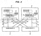
- FIG. 2 there is shown a block diagram illustrating in detail the scheme of the connection with the shared memories.
- This diagram shows CHAs 11 and 12 (or, with DKAs, sometimes referred to as adapters), which are subsystems having processors, duplicate shared memories 21 and 22, which are peripheral units (shared modules), and access paths 31, 32, 33, 34, 35, 36, 37, and 38 for connecting the CHAs (DKAs) 11 and 12 with the shared memories 21 and 22.
- the CHAs (DKAs) have path selection control circuits 41 and 42 and path mode setting registers 51 and 52 respectively.
- the shared memories 21 and 22 are duplicate and therefore, if one of them fails and then closed down, the system operation can be continued with the other normal shared memory with some degraded performance if any.
- Access by the CHA (DKA) 11 for example to the shared memory 21 can be made through both the access path 31 and the access path 32.
- DKA CHA
- two connection paths are provided between each processor and each shared memory, each access path functioning independently of each other, thereby ensuring individual access when the system is normally operating.
- path selection control circuit 41 or 42 When access to any shared memory is instructed by a processor, its path selection control circuit 41 or 42 references the content of its path mode setting register 51 or 52 to determine the access path to be used for the instructed access operation.
- the path mode setting registers 51 and 52 each consist of four bits, which correspond to the four access paths connected to that processor.
- the path mode setting registers 51 and 52 are programmable; normally, the four bits are all set to "0"s, meaning path automatic distribution. If zero specification can be referenced by the path selection control circuit, a path that was not used by the last access is used preferentially. Consequently, the access load of the shared memory is distributed over the two access paths, thereby enhancing access performance.
- the path mode setting registers 51 and 52 are set by program to the path fixed mode. For example, when the two bits corresponding to the shared memory 21 are set to "1" and "0" and the shared memory 21 is accessed, the path selection control circuits 41 and 42 selects in a fixed manner the first access paths (the access path 31 of the CHA 11 or the DKA 11 and the access path 35 of the CHA 12 or the DKA 12).
- FIG. 3 there are shown the setting values of the path mode registers 51 and 52 and the access paths to be selected for these setting values.
- "Distributed path” in the figure denotes that a path not used in the last access is selected for load distribution as described above.
- each access bus can operate independently of each other. Therefore, access contention for certain data in the shared memory may occur. Especially, if a contention occurs during a read-modify-write operation, data integrity may be destroyed.
- the read-modify-write operation denotes reading certain data in the shared memory and writing this data with a specific bit turned on for example. For example, if data to be read for manipulation is rewritten by another write access operation before this data is rewritten, the rewriting is made invalid by a later write operation. Thus, if access exclusive control is not performed through another path during a sequence of operations, data integrity cannot be ensured.
- the apparatus is provided with an address locking unit in hardware approach.
- this address locking unit when a read-modify-write command comes, an address to be accessed is set in the address locking unit, thereby indicating that this address is in the locked state.
- address locking is set, all other memory accesses are checked for address locking. If the address to be accessed is found in the locked state, the memory access concerned waits until the address is unlocked. The memory access concerned is executed after unlocking of that address.
- round robin control operates to prevent lock time-out from occurring.
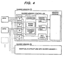
- FIG. 4 there is shown a block diagram illustrating a constitution of the controller including this address locking unit in the shared memory.
- a shared memory 1 in FIG. 4 is identical with a shared memory plane A shown in FIG. 2 and a shared memory 2 is identical with a shared memory plane B shown in FIG. 2 .
- the shared memory shown in FIG. 1 is duplexed into shared memory planes A and B.
- a shared memory control LSI has a contention controller for controlling the above-mentioned contention, a memory controller, an ECC generator, an ECC checking block, and so on.
- the shared memory control LSI In a data write operation, the shared memory control LSI generates a check code called ECC (Error Check Condition) and checks ECC integrity in a data read operation, thereby preventing data from being destroyed by memory fault.
- ECC Error Check Condition
- exclusive control is executed in a predetermined address range.
- the address to be accessed is registered to put it in the locked state.
- the address to be accessed is compared with the locked address. If a match is found, this later access request is kept in the wait state until the locked address is unlocked. Thus, data integrity can be retained.
- the shared memory access exclusive scheme based on this address locking is shown in FIG. 5 .
- the processor of MP#1 in order to execute a read-modify-write operation, issues a locked access command.
- this command is a locked read command.
- the shared memory receives the locked read command, the shared memory performs an access path fixing operation to prevent a same address from being accessed through other access paths. Then, the shared memory reads the memory as instructed by the received read command and returns the read data and its status to the MP#1.
- MP#1 modifies the data and issues a write command to the shared memory. Then, receiving the status from the shared memory, the MP#1 processes it and issues an unlocking command to the shared memory. This unlocking command allows the shared memory to receive access from other paths.
- the processor of the MP#2 attempting to access the same address when the shared memory is in the locked state enters the lock wait state when the access by the MP#1 is in the locked state.
- the MP#1 is unlocked, the memory write operation is executed.
- the MP#1 and the MP#2 denote the processors in any CHAs or DKAs and are identical with those shown in FIG. 2 .
- the following describes fault tolerant control to be executed if an access error is caused by hardware fault when the processor of the DKA 12 accesses the shared memory 21 through the access path 35.
- a fault location can be clearly determined from the hardware information present at the fault occurrence. For example, if the fault is now judged located inside the processor of the DKA 12, the DKA 12 is isolated from the system, continuing the system operation by use of the processor of the other DKA. If the fault is judged located inside the shared memory 21 for example from the fault information, the shared memory 21 is isolated from the system, continuing the system operation by use of the shared memory 22.
- a fault location cannot be cleared identified only from fault information. For example, assume that a time-out error occur during a write access operation to the shared memory 21 by the processor of the DKA 12 through the access path 35 and therefore a normal end be not reported. If this happens, it cannot be clearly determined only from the fact that the time-out error occurred whether a write command has not been sent to the controller of the shared memory 21 due to a fault of the processor in the DKA 12, the normal end has not been reported due to a fault of the shared memory 21, or information has not been normally transmitted due to a fault of the access path 35.
- the system according to the invention performs an access test in fault processing to totally determine whether the shared memory access through each path is normal or not, thereby identifying the fault location and isolating the identified fault.
- the access path 35 is put out of use. Thereafter, until the access path 35 is recovered by maintenance job, the DKA 12 accesses the shared memory 21 through the access path 36.
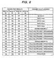
- Paths 1A(a), 1A(b), 1B(a), and 1B(b) shown in FIG. 6 correspond to the access paths 31, 32, 33, and 34 for example shown in FIG. 2 .
- the fault location can be identified for sure.
- the fault of the shared memory or the processor of the CHA or DKA may also be identified in most cases because it is almost impossible for two or more access paths to fail at a time. Namely, arranging these combinations into a table and searching the table from the results of an access test allows a quick identification of a fault location to be blocked for fault recovery.
- FIG. 7 there is shown a flowchart indicative of the above-mentioned fault identification method.
- step 701 When a fault is detected (step 701), the information about the detected fault is gathered (step 702). Based on the gathered information, it is judged whether the fault location is obvious or not (step 703). If the fault location is obvious, the fault location is blocked (step 711), thereby completing the fault recovery (step 712).
- step 704 access is retried (step 704) to determine whether the access is successful or not (step 705). If the access is successful, it is judged that the fault is only temporary (step 712), upon which the fault recovery is completed (step 713). If the access is unsuccessful again, an access test is performed on the path 1-shared memory (A) to the path 2-shared memory (B) (for example, the path 1A(a) to the path 1B(b) shown in FIG. 6 ) (steps 706 through 709) to judge the fault location with reference to the table shown in FIG. 6 (step 710). Then, the identified fault location is blocked (step 711) to complete the fault recovery (step 712). It should be noted that steps 706 through 709 may not be executed especially sequentially as long as an access path test associated with a fault location is executed.
- the fault recovery of an access path fault based on the method according to the invention allows to block the fault path without affecting or interrupting the access by other processors within the system.
- the present invention may also be applied to the connection between the host computer, which is a subsystem, and the storage apparatus, which is a peripheral unit.
- the storage apparatus is multiplexed and two connection paths are provided for each host computer and each storage apparatus.
- an access test is performed on another path to the same storage apparatus and on a path connected to another storage apparatus. The result of this access test is matched against the table shown in FIG. 6 to judge whether the fault is on the entire storage apparatus or on a connection system such as channel.
- problems caused by shared bus connection in an information processing apparatus having multiple processors can be solved.
- the present invention can solve problems in identifying fault locations caused at connection in a general individual bus connection scheme. Consequently, the present invention provides the connection means that satisfy both performance and reliability requirements.
- the multiple individual path connection scheme makes all the communication paths between the processors and the component modules independent of each other, thereby preventing a single fault from propagating over the entire system. Still further, the plurality of communication paths can operate not in a time division manner but in parallel at a time, thereby solving the problem of performance degradation caused by the shared bus.
Abstract
Description
- The present invention relates generally to a fault recovery method for a storage apparatus of a computer-based information processing system or a computer-based information processing apparatus and is associated with fault detection and fault recovery for ensuring the continuation of a desired operation of the system as a whole even if the storage apparatus, a component of the system, fails. More particularly, the present invention relates to a linking technology for linking a processor with a shared module in a multiprocessor system and a fault tolerance control technology based on the linking technology.
- Today, with computer-based information processing systems being in wide use through general society, their faults will result in extremely serious social troubles. On the other hand, as the scale of these systems increases, it is almost impossible to make the systems fault-free. Consequently, it is required for every information processing system to continue as a whole a desired operation even if the system fails partially.
- To realize this requirement, Papers of "Information Processing Society of Japan" Vol. 34, No. 11, Nov., 1993, pp. 1375 to 1384, "Realtime Video Signal Processor And Its Application" (Nobuyuki Yagi), "2.3 Connecting Schemes," "
Fig. 3 Processor-to-Processor Connection" proposes information processing system architectures including (a) "Bus" scheme as "shared bus connecting" for connecting system component modules with a shared bus, (d) "Complete" scheme as "individual path connecting" for connecting modules necessary for linking with an individual path, and so on. - Further,
Japanese Patent Laid-open No. Hei 9-160723 - On the other hand, in the individual path connecting scheme, the connecting paths between the processors and the shared modules in a system are independent of each other and therefore the fault of one path will not generally affect the entire system.
-
US-5 790 775 discloses a storage controller having the features recited in the precharacterising first part of claim 3 in common with the present invention. The storage controller of this prior art consists of two controllers each having access to the cache memory of the other. Each controller includes a-shared memory for use by its internal units. Both controllers exchange "keep alive" messages. A controller failing to receive the "keep alive" messages of the other, reports to the host computer that a fault has occurred in the other controller, destages the cache contents of the other controller to the disk devices and listens to commands addressed to the failed controller. - In the shared bus connecting, since the bus signal line of a system is basically time-shared by a plurality of processors and a plurality of component modules, a plurality of signals cannot be sent simultaneously. Therefore, especially with a controller which requires high performance, its bus limitation imposes a system performance bottleneck. In addition, because the shared bus system is a shared resource in a system, the occurrence of a fault inevitably affects the entire system.
- In the individual path connecting, there is only one communication path between each processor and a shared module, so that no test by communication path switching can be performed. Consequently, faults of some types disable correct isolation of fault location to ensure the continuous operation of a system.
- If, in an attempt to solve this problem, a plurality of individual paths are simply provided between each processor and a shared module in a multiprocessor system having a shared memory, a plurality of access requests generated in a same processor package and an access request generated in each processor are mixed into the shared memory. And, if an access is made to data stored in the same shared memory while the data is being exclusively accessed for read modify write for example, the integrity of the data is destroyed.
- It is therefore an object of the invention to provide a method for recovery from a fault in an information processing apparatus comprising a plurality of processors, with improved data integrity and performance, and to provide a storage controller based on this method.
- This object is solved by the method of
claim 1 and the storage controller of claim 3. The dependent claims relate to preferred embodiments of the invention. - An embodiment of the present invention provides, in an information processing apparatus having multiple processors, a method of connecting a plurality of individual paths capable of ensuring data integrity.
- In carrying out the invention and according to one embodiment thereof, there is provided a multiple individual path connecting method in which two or more connection paths are provided between each processor and each shared module in the system. If a fault is detected, tests are made by switching between the communication paths to totally judge a fault location.
- For the plurality of connection paths between each processor and each shared module, access path switching and address locking are provided.
- In the address locking, a system shared module such as a shared memory is arranged with an address locking unit to perform exclusive control in a predetermined address range. If a request for access requiring address exclusive control is made, the access address is registered to indicate that the address is in a locked state. When another access request is made to the locked address, the access address is compared with the locked address. If the access address is found matching the locked address, the access is held in a wait state until the address is unlocked and the access is made again after the address locking is cleared, thereby ensuring data integrity.
- These and other objects of the invention will be explained with reference to the description, taken in connection with the accompanying drawing, in which:
-
FIG. 1 is a system schematic diagram illustrating an information processing apparatus practiced as one preferred embodiment of the invention; -
FIG. 2 is a block diagram illustrating main connecting units of the information processing apparatus shown inFIG. 1 ; -
FIG. 3 is a table of combinations of path mode setting register values and access paths to be selected; -
FIG. 4 is a block diagram illustrating a constitution of a shared memory controller; -
FIG. 5 is a diagram illustrating an address locking method and an exclusive access method; -
FIG. 6 is a table of combinations of access test results and assumed fault locations; and -
FIG. 7 is a flowchart indicative of fault detection to judge fault location. - This invention will be described in further detail by way of example with reference to the accompanying drawings.
- Now, referring to
FIG. 1 , there is shown a system schematic diagram illustrating the hierarchy of a storage apparatus practiced as one preferred embodiment. The storage apparatus comprises achannel connection system 1 for connection to a host computer, not shown, which is a higher-level apparatus, acache memory 2 for temporarily storing input/output data, a channel adapter (hereafter referred to as CHA) for controlling the data transfer between thechannel connection system 1 and thecache memory 2, a disk array 4, which is a storage medium for storing data, a disk adapter (hereafter referred to as DKA) for controlling the data transfer between thecache memory 2 and the disk array 4, and a sharedmemory 6 provided between the CHA 3 and the DKA 5. The sharedmemory 6 will be detailed later. -
FIG. 1 is schematic and therefore does not illustrate detail connections. Actually, thecache memory 2 and the sharedmemory 6 are connected to one CHA or (DKA). It should be noted that the channel connection system includes, for example, a channel controller in the case of the connection with a mainframe-type host computer (CKD data format) and a SCSI bus controller in the case of the connection with a UNIX-type computer (FBA data format). Alternatively, a controller based on fiber channel may be available. - The shared
memory 6 stores control information such as the directory information (a hierarchical table for cache segment search, and the state of each segment) for controlling the use of thecache memory 2, processor-to-processor communication messages (the contents of communication to be executed for the cooperation and synchronization between processors) between the CHA 3 and the DKA 5, system configuration information (the common information associated with the system configuration states such as the mounting states of the CHA 3 and the DKA 5 existing in the system, the storage sizes of thecache memory 2 and the sharedmemory 6, and the number of disk arrays 4). - The following describes the basic operation of the storage apparatus.
- The CHA 3 receives a command from the host computer through the
channel connection system 1, interprets the received command, and controls data transfer. The following describes the basic operation to be performed when the CHA 3 receives a read command for data for example from the host computer. - First, the CHA 3 accesses the shared
memory 6 to check thecache memory 2 for the data to be read. If the target data is found in thecache memory 2, the CHA 3 transfers this data to the host computer from thecache memory 2 through thechannel connection system 1. If the target data is not found, the CHA 3 uses the sharedmemory 6 to perform processor-to-processor communication with the DKA 5. The DKA 5 transfers the target data from the disk array 4 to thecache memory 2. For the segment for which the data transfer has been completed, the DKA 5 accesses the sharedmemory 6 again to make communication with the CHA 3, which then controls the data transfer from thecache memory 2 to the host computer. - The CHA 3 and the DKA 5 existing in plurality in the system have each a processor. The connection from each processor to the shared
memory 6 is provided independently of each other. In addition, in order to prevent a system operation halt from occurring due to a single fault, the sharedmemory 6 is also arranged in plural to provide redundancy. - The following describes the connection system between each processor and each shared
memory 6. - Referring to
FIG. 2 , there is shown a block diagram illustrating in detail the scheme of the connection with the shared memories. This diagram shows CHAs 11 and 12 (or, with DKAs, sometimes referred to as adapters), which are subsystems having processors, duplicate sharedmemories access paths memories selection control circuits - The shared
memories - Access by the CHA (DKA) 11 for example to the shared
memory 21 can be made through both theaccess path 31 and theaccess path 32. Thus, two connection paths are provided between each processor and each shared memory, each access path functioning independently of each other, thereby ensuring individual access when the system is normally operating. - The following describes the capabilities of the path
selection control circuits - When access to any shared memory is instructed by a processor, its path
selection control circuit mode setting register - If one of the paths is made unavailable by a fault or other causes, the path mode setting registers 51 and 52 are set by program to the path fixed mode. For example, when the two bits corresponding to the shared
memory 21 are set to "1" and "0" and the sharedmemory 21 is accessed, the pathselection control circuits access path 31 of theCHA 11 or theDKA 11 and theaccess path 35 of theCHA 12 or the DKA 12). - Referring to
FIG. 3 , there are shown the setting values of the path mode registers 51 and 52 and the access paths to be selected for these setting values. "Distributed path" in the figure denotes that a path not used in the last access is selected for load distribution as described above. - Unlike the shared bus connection scheme, each access bus can operate independently of each other. Therefore, access contention for certain data in the shared memory may occur. Especially, if a contention occurs during a read-modify-write operation, data integrity may be destroyed.
- The read-modify-write operation denotes reading certain data in the shared memory and writing this data with a specific bit turned on for example. For example, if data to be read for manipulation is rewritten by another write access operation before this data is rewritten, the rewriting is made invalid by a later write operation. Thus, if access exclusive control is not performed through another path during a sequence of operations, data integrity cannot be ensured.
- To ensure data integrity, the apparatus according to the invention is provided with an address locking unit in hardware approach. With this address locking unit, when a read-modify-write command comes, an address to be accessed is set in the address locking unit, thereby indicating that this address is in the locked state. When address locking is set, all other memory accesses are checked for address locking. If the address to be accessed is found in the locked state, the memory access concerned waits until the address is unlocked. The memory access concerned is executed after unlocking of that address.
- If two or more processors are put in the lock wait state, round robin control operates to prevent lock time-out from occurring.
- Referring to
FIG. 4 , there is shown a block diagram illustrating a constitution of the controller including this address locking unit in the shared memory. It should be noted that, in the figure, a sharedmemory 1 inFIG. 4 is identical with a shared memory plane A shown inFIG. 2 and a sharedmemory 2 is identical with a shared memory plane B shown inFIG. 2 . The shared memory shown inFIG. 1 is duplexed into shared memory planes A and B. - A shared memory control LSI has a contention controller for controlling the above-mentioned contention, a memory controller, an ECC generator, an ECC checking block, and so on. In a data write operation, the shared memory control LSI generates a check code called ECC (Error Check Condition) and checks ECC integrity in a data read operation, thereby preventing data from being destroyed by memory fault.
- Then, in the address locking unit, exclusive control is executed in a predetermined address range. To be more specific, when an access requiring address exclusive control is requested, the address to be accessed is registered to put it in the locked state. Then, when another access requests comes in this state, the address to be accessed is compared with the locked address. If a match is found, this later access request is kept in the wait state until the locked address is unlocked. Thus, data integrity can be retained.
- The shared memory access exclusive scheme based on this address locking is shown in
FIG. 5 . Here, the processor ofMP# 1, in order to execute a read-modify-write operation, issues a locked access command. In this case, this command is a locked read command. Receiving the locked read command, the shared memory performs an access path fixing operation to prevent a same address from being accessed through other access paths. Then, the shared memory reads the memory as instructed by the received read command and returns the read data and its status to theMP# 1.MP# 1 modifies the data and issues a write command to the shared memory. Then, receiving the status from the shared memory, theMP# 1 processes it and issues an unlocking command to the shared memory. This unlocking command allows the shared memory to receive access from other paths. - Namely, the processor of the
MP# 2 attempting to access the same address when the shared memory is in the locked state enters the lock wait state when the access by theMP# 1 is in the locked state. When theMP# 1 is unlocked, the memory write operation is executed. It should be noted that, inFIG. 5 , theMP# 1 and theMP# 2 denote the processors in any CHAs or DKAs and are identical with those shown inFIG. 2 . - The following describes fault tolerant control to be executed if an access error is caused by hardware fault when the processor of the
DKA 12 accesses the sharedmemory 21 through theaccess path 35. - First, there is a case in which a fault location can be clearly determined from the hardware information present at the fault occurrence. For example, if the fault is now judged located inside the processor of the
DKA 12, theDKA 12 is isolated from the system, continuing the system operation by use of the processor of the other DKA. If the fault is judged located inside the sharedmemory 21 for example from the fault information, the sharedmemory 21 is isolated from the system, continuing the system operation by use of the sharedmemory 22. - However, there may be a case in which, with a system consisting of a plurality of hardware configurations, a fault location cannot be cleared identified only from fault information. For example, assume that a time-out error occur during a write access operation to the shared
memory 21 by the processor of theDKA 12 through theaccess path 35 and therefore a normal end be not reported. If this happens, it cannot be clearly determined only from the fact that the time-out error occurred whether a write command has not been sent to the controller of the sharedmemory 21 due to a fault of the processor in theDKA 12, the normal end has not been reported due to a fault of the sharedmemory 21, or information has not been normally transmitted due to a fault of theaccess path 35. - If such a case in which the fault location is ambiguous occurred, the system according to the invention performs an access test in fault processing to totally determine whether the shared memory access through each path is normal or not, thereby identifying the fault location and isolating the identified fault.
- To be more specific, if a fault is detected in the
DKA 12, access to the sharedmemory 21 through theaccess path 35, access to the sharedmemory 21 through theaccess path 36, access to the sharedmemory 22 through theaccess path 37, and access to the sharedmemory 22 through theaccess path 38 are attempted. The fault location is judged based on whether each of these four patterns of access operations has ended normally or not. - For example, if the fault occurred only when accessing the shared
memory 21 through theaccess path 35 and normal access is enabled when accessing the sharedmemory 21 through theaccess path 36, it is judged that fault is only on theaccess path 35. When this determination is made, theaccess path 35 is put out of use. Thereafter, until theaccess path 35 is recovered by maintenance job, theDKA 12 accesses the sharedmemory 21 through theaccess path 36. - Assume again that the access operations to the shared
memory 21 through theaccess paths memory 22 can be normally accessed through theaccess path memory 21, upon which the sharedmemory 21 is blocked. Thereafter, until the sharedmemory 21 is recovered by maintenance job, each processor does not use the sharedmemory 21 but uses the sharedmemory 22 for information transmission and other operations. - Assume further that the access operation to the shared
memory 21 through theaccess paths memory 22 through theaccess paths DKA 12 and therefore the processor concerned is blocked. - Referring to
FIG. 6 , there is shown a table listing combinations of the results of the above-mentioned access tests and assumed fault locations which must be isolated from the system.Paths 1A(a), 1A(b), 1B(a), and 1B(b) shown inFIG. 6 correspond to theaccess paths FIG. 2 . In these combinations, in the case of the fault of an access path alone, the fault location can be identified for sure. For the fault of the shared memory or the processor of the CHA or DKA may also be identified in most cases because it is almost impossible for two or more access paths to fail at a time. Namely, arranging these combinations into a table and searching the table from the results of an access test allows a quick identification of a fault location to be blocked for fault recovery. - It should be noted that it is possible to judge whether a fault is on an access path alone or not only by performing an access path test to the same shared memory through another access path before testing all access paths. This is because, if tests on two or more access paths to different shared memories result in no good, a multiple fault is highly possible, which makes fault identification difficult.
- Referring to
FIG. 7 , there is shown a flowchart indicative of the above-mentioned fault identification method. - When a fault is detected (step 701), the information about the detected fault is gathered (step 702). Based on the gathered information, it is judged whether the fault location is obvious or not (step 703). If the fault location is obvious, the fault location is blocked (step 711), thereby completing the fault recovery (step 712).
- If the fault location is not obvious, access is retried (step 704) to determine whether the access is successful or not (step 705). If the access is successful, it is judged that the fault is only temporary (step 712), upon which the fault recovery is completed (step 713). If the access is unsuccessful again, an access test is performed on the path 1-shared memory (A) to the path 2-shared memory (B) (for example, the
path 1A(a) to thepath 1B(b) shown inFIG. 6 ) (steps 706 through 709) to judge the fault location with reference to the table shown inFIG. 6 (step 710). Then, the identified fault location is blocked (step 711) to complete the fault recovery (step 712). It should be noted thatsteps 706 through 709 may not be executed especially sequentially as long as an access path test associated with a fault location is executed. - Unlike the connection scheme based on shared bus, the fault recovery of an access path fault based on the method according to the invention allows to block the fault path without affecting or interrupting the access by other processors within the system.
- In the above description of the preferred embodiment of the invention, only the connection between the processor and shared memory in the storage controller has been shown. It will be apparent to those skilled in the art that the present invention is also applicable to the connection to such shared components of the storage apparatus as the cache memory, in addition to the shared memory.
- Further, the present invention may also be applied to the connection between the host computer, which is a subsystem, and the storage apparatus, which is a peripheral unit. In this case, the storage apparatus is multiplexed and two connection paths are provided for each host computer and each storage apparatus. When an error is reported, an access test is performed on another path to the same storage apparatus and on a path connected to another storage apparatus. The result of this access test is matched against the table shown in
FIG. 6 to judge whether the fault is on the entire storage apparatus or on a connection system such as channel. - As described and according to the invention, problems caused by shared bus connection in an information processing apparatus having multiple processors can be solved. In addition, the present invention can solve problems in identifying fault locations caused at connection in a general individual bus connection scheme. Consequently, the present invention provides the connection means that satisfy both performance and reliability requirements.
- Further, the multiple individual path connection scheme makes all the communication paths between the processors and the component modules independent of each other, thereby preventing a single fault from propagating over the entire system. Still further, the plurality of communication paths can operate not in a time division manner but in parallel at a time, thereby solving the problem of performance degradation caused by the shared bus.
- While the preferred embodiments of the present invention have been described using specific terms, such description is for illustrative purposes only, and it is to be understood that changes and variations may be made without departing from the scope of the appended claims.
Claims (6)
- A method for recovery from a fault in an information processing apparatus comprising first and second processors (11, 12), first and second shared memories (21, 22) provided in duplicate for storing control information for the processors, and a plurality of access paths (31 to 38) interconnecting the processors and the shared memories, the method comprising the following steps executed when a fault occurs in an access from a processor (11, 12) to a shared memory (21, 22):a first access step (706) of accessing said first shared memory by a first access path,a second access step (708) of accessing said first shared memory by a second access path provided independently from the first access path,a third access step (707) of accessing said second shared memory by a third access path,a fourth access step (709) of accessing said second shared memory by a fourth access path provided independently from said third access path,matching the results of the first to fourth access steps against combinations of access test results and assumed fault locations, to determine (710) whether the location of said occurred fault is in any of said access paths, said shared memories or said processors, andsetting a register (51, 52) to make one or more of said access paths unavailable so as to block (711) said fault location.
- The method of claim 1, further comprising the following steps:gathering (701) information about said fault and, if the fault location is obvious, blocking the fault location,if the fault location is not obvious, retrying (704) said access and, if the fault occurs again, executing the steps (706 to 711) of claim 1.
- A storage controller comprising:first and second adapters (11, 12) respectively comprising first and second processors for receiving a command from another apparatus,first and second shared memories (21, 22), anda plurality of access paths (31 to 38) interconnecting said processors and said shared memories,characterised in thatsaid shared memories (21, 22) are provided in duplicate for storing control information for said processors to control storage of data in a cache memory (2),said access paths include a first access path and a second access path provided independently, each for connecting a said processor with said first shared memory, and a third access path and a fourth access path provided independently, each for connecting said processor with said second shared memory, and there are provided matching means for matching the results of the first to fourth access paths against combinations of access test results and assumed fault locations and determining whether the location of said occurred fault is in any of said access paths, said shared memories or said processors, and means for setting a register (51, 52) to make one or more of said access paths unavailable so as to block said fault location.
- The storage controller of claim 3, whereinsaid other apparatus is a host apparatus (1) and said adapter is a channel adapter (11, 12) for receiving a command from said host apparatus.
- The storage controller of claim 3, whereinsaid other apparatus is a disk array (4) for storing data and said adapter is a disk adapter (11, 12) for transferring data from said disk array to said cache memory (2).
- The storage controller of any of claims 3 to 5, whereinsaid processors are each adapted to issue a locked access command to each of said shared memories (21, 22) when executing predetermined processing, and to effect unlocking after completion of said predetermined processing.
Applications Claiming Priority (2)
| Application Number | Priority Date | Filing Date | Title |
|---|---|---|---|
| JP35725498 | 1998-12-16 | ||
| JP35725498A JP4132322B2 (en) | 1998-12-16 | 1998-12-16 | Storage control device and control method thereof |
Publications (3)
| Publication Number | Publication Date |
|---|---|
| EP1011047A2 EP1011047A2 (en) | 2000-06-21 |
| EP1011047A3 EP1011047A3 (en) | 2006-07-12 |
| EP1011047B1 true EP1011047B1 (en) | 2008-07-09 |
Family
ID=18453188
Family Applications (1)
| Application Number | Title | Priority Date | Filing Date |
|---|---|---|---|
| EP99117283A Expired - Lifetime EP1011047B1 (en) | 1998-12-16 | 1999-09-02 | Fault recovery method and storage controller in information processing apparatus |
Country Status (4)
| Country | Link |
|---|---|
| US (1) | US7302606B2 (en) |
| EP (1) | EP1011047B1 (en) |
| JP (1) | JP4132322B2 (en) |
| DE (1) | DE69939050D1 (en) |
Families Citing this family (21)
| Publication number | Priority date | Publication date | Assignee | Title |
|---|---|---|---|---|
| JP2003288279A (en) | 2002-03-28 | 2003-10-10 | Hitachi Ltd | Fault detection method between storage device and storage device used for it |
| US7565566B2 (en) * | 2003-04-23 | 2009-07-21 | Dot Hill Systems Corporation | Network storage appliance with an integrated switch |
| US7627780B2 (en) | 2003-04-23 | 2009-12-01 | Dot Hill Systems Corporation | Apparatus and method for deterministically performing active-active failover of redundant servers in a network storage appliance |
| US7380163B2 (en) * | 2003-04-23 | 2008-05-27 | Dot Hill Systems Corporation | Apparatus and method for deterministically performing active-active failover of redundant servers in response to a heartbeat link failure |
| US7401254B2 (en) * | 2003-04-23 | 2008-07-15 | Dot Hill Systems Corporation | Apparatus and method for a server deterministically killing a redundant server integrated within the same network storage appliance chassis |
| JP4454299B2 (en) * | 2003-12-15 | 2010-04-21 | 株式会社日立製作所 | Disk array device and maintenance method of disk array device |
| US7450959B2 (en) * | 2003-12-31 | 2008-11-11 | Qualcomm Incorporated | Wireless multiprocessor system-on-chip with unified memory and fault inhibitor |
| JP4585217B2 (en) * | 2004-03-29 | 2010-11-24 | 株式会社日立製作所 | Storage system and control method thereof |
| JP2006244123A (en) * | 2005-03-03 | 2006-09-14 | Fujitsu Ltd | Data storage system and data storage control device |
| JP4461485B2 (en) * | 2005-04-05 | 2010-05-12 | 株式会社ジェイテクト | Distributed control device |
| JP4645278B2 (en) | 2005-04-15 | 2011-03-09 | ソニー株式会社 | Optical signal processing device |
| US7590885B2 (en) * | 2005-04-26 | 2009-09-15 | Hewlett-Packard Development Company, L.P. | Method and system of copying memory from a source processor to a target processor by duplicating memory writes |
| JP4414399B2 (en) * | 2006-01-30 | 2010-02-10 | 富士通株式会社 | Disk controller |
| US8055856B2 (en) * | 2008-03-24 | 2011-11-08 | Nvidia Corporation | Lock mechanism to enable atomic updates to shared memory |
| JP5966243B2 (en) | 2010-12-20 | 2016-08-10 | 富士通株式会社 | Storage device and storage device control method |
| JP5738471B2 (en) * | 2011-12-14 | 2015-06-24 | 株式会社日立製作所 | Storage apparatus and memory control method thereof |
| US20150248320A1 (en) * | 2014-02-28 | 2015-09-03 | Red Hat Israel, Ltd. | Host-storage connectivity monitoring |
| US10528435B2 (en) * | 2017-05-08 | 2020-01-07 | International Business Machines Corporation | Performance efficient time locks on data in a storage controller |
| US10489080B2 (en) | 2017-05-08 | 2019-11-26 | International Business Machines Corporation | Point in time copy of time locked data in a storage controller |
| US10514721B2 (en) | 2017-05-08 | 2019-12-24 | International Business Machines Corporation | Validation of clock to provide security for time locked data |
| US10514859B2 (en) | 2017-05-08 | 2019-12-24 | International Business Machines Corporation | Reduction of processing overhead for point in time copy to allow access to time locked data |
Family Cites Families (18)
| Publication number | Priority date | Publication date | Assignee | Title |
|---|---|---|---|---|
| US3623014A (en) * | 1969-08-25 | 1971-11-23 | Control Data Corp | Computer communications system |
| US5680574A (en) * | 1990-02-26 | 1997-10-21 | Hitachi, Ltd. | Data distribution utilizing a master disk unit for fetching and for writing to remaining disk units |
| US5155845A (en) * | 1990-06-15 | 1992-10-13 | Storage Technology Corporation | Data storage system for providing redundant copies of data on different disk drives |
| US5638506A (en) * | 1991-04-08 | 1997-06-10 | Storage Technology Corporation | Method for logically isolating a cache memory bank from a memory bank group |
| US5392425A (en) * | 1991-08-30 | 1995-02-21 | International Business Machines Corporation | Channel-initiated retry and unit check for peripheral devices |
| JP2777301B2 (en) * | 1992-01-07 | 1998-07-16 | 三菱電機株式会社 | Recording device |
| US5581724A (en) * | 1992-10-19 | 1996-12-03 | Storage Technology Corporation | Dynamically mapped data storage subsystem having multiple open destage cylinders and method of managing that subsystem |
| US5572694A (en) * | 1992-11-25 | 1996-11-05 | Fujitsu Limited | Virtual system for detecting access paths belonging to same group from plurality of access paths to reach device designated by command with reference to table |
| US5771367A (en) * | 1992-12-17 | 1998-06-23 | International Business Machines Corporation | Storage controller and method for improved failure recovery using cross-coupled cache memories and nonvolatile stores |
| US5473752A (en) * | 1993-03-17 | 1995-12-05 | Detector Electronics Corporation | Fault isolation circuit |
| US5390326A (en) * | 1993-04-30 | 1995-02-14 | The Foxboro Company | Local area network with fault detection and recovery |
| JP3264465B2 (en) * | 1993-06-30 | 2002-03-11 | 株式会社日立製作所 | Storage system |
| US5790775A (en) * | 1995-10-23 | 1998-08-04 | Digital Equipment Corporation | Host transparent storage controller failover/failback of SCSI targets and associated units |
| JP3628777B2 (en) * | 1995-10-30 | 2005-03-16 | 株式会社日立製作所 | External storage device |
| US6032271A (en) * | 1996-06-05 | 2000-02-29 | Compaq Computer Corporation | Method and apparatus for identifying faulty devices in a computer system |
| JP3581765B2 (en) * | 1996-09-20 | 2004-10-27 | 株式会社日立コミュニケーションテクノロジー | Path switching method and apparatus in complex ring network system |
| US5890219A (en) * | 1996-11-27 | 1999-03-30 | Emc Corporation | Redundant writing of data to cached storage system |
| US5862308A (en) * | 1996-12-03 | 1999-01-19 | Bull Hn Information Systems Inc. | Fault intercept and resolution process independent of operating system |
-
1998
- 1998-12-16 JP JP35725498A patent/JP4132322B2/en not_active Expired - Fee Related
-
1999
- 1999-09-02 EP EP99117283A patent/EP1011047B1/en not_active Expired - Lifetime
- 1999-09-02 DE DE69939050T patent/DE69939050D1/en not_active Expired - Fee Related
-
2003
- 2003-06-23 US US10/600,828 patent/US7302606B2/en not_active Expired - Fee Related
Also Published As
| Publication number | Publication date |
|---|---|
| JP2000181887A (en) | 2000-06-30 |
| EP1011047A2 (en) | 2000-06-21 |
| DE69939050D1 (en) | 2008-08-21 |
| EP1011047A3 (en) | 2006-07-12 |
| JP4132322B2 (en) | 2008-08-13 |
| US20040153691A1 (en) | 2004-08-05 |
| US7302606B2 (en) | 2007-11-27 |
Similar Documents
| Publication | Publication Date | Title |
|---|---|---|
| EP1011047B1 (en) | Fault recovery method and storage controller in information processing apparatus | |
| US6725331B1 (en) | Method and apparatus for managing the dynamic assignment resources in a data storage system | |
| US4503535A (en) | Apparatus for recovery from failures in a multiprocessing system | |
| US7600152B2 (en) | Configuring cache memory from a storage controller | |
| US5502728A (en) | Large, fault-tolerant, non-volatile, multiported memory | |
| US4907228A (en) | Dual-rail processor with error checking at single rail interfaces | |
| US5255367A (en) | Fault tolerant, synchronized twin computer system with error checking of I/O communication | |
| US4916704A (en) | Interface of non-fault tolerant components to fault tolerant system | |
| US4958273A (en) | Multiprocessor system architecture with high availability | |
| EP0306244B1 (en) | Fault tolerant computer system with fault isolation | |
| EP0348994A2 (en) | Directed hardware error identification method and apparatus for error recovery in piplined processing areas of a computer system | |
| US6874046B1 (en) | Method and apparatus for enhancing access to redundant data storage facilities | |
| US5235687A (en) | Method for replacing memory modules in a data processing system, and data processing system for performing the method | |
| US7127638B1 (en) | Method and apparatus for preserving data in a high-availability system preserving device characteristic data | |
| US7117320B2 (en) | Maintaining data access during failure of a controller | |
| US6643734B2 (en) | Control device and control method for a disk array | |
| JP2000181887A5 (en) | ||
| US6801983B2 (en) | Disk control device and storage device using it | |
| KR100258079B1 (en) | The duplicated device by extention of memory bus in a tightly coupled fault tolerance system | |
| US7752340B1 (en) | Atomic command retry in a data storage system | |
| US5630045A (en) | Device and method for fault tolerant dual fetch and store | |
| US7472221B1 (en) | Mirrored memory | |
| US7302526B1 (en) | Handling memory faults for mirrored memory | |
| JPS6119061B2 (en) | ||
| JP4708669B2 (en) | Path redundancy apparatus and method |
Legal Events
| Date | Code | Title | Description |
|---|---|---|---|
| PUAI | Public reference made under article 153(3) epc to a published international application that has entered the european phase |
Free format text: ORIGINAL CODE: 0009012 |
|
| AK | Designated contracting states |
Kind code of ref document: A2 Designated state(s): AT BE CH CY DE DK ES FI FR GB GR IE IT LI LU MC NL PT SE |
|
| AX | Request for extension of the european patent |
Free format text: AL;LT;LV;MK;RO;SI |
|
| 17P | Request for examination filed |
Effective date: 20060331 |
|
| PUAL | Search report despatched |
Free format text: ORIGINAL CODE: 0009013 |
|
| AK | Designated contracting states |
Kind code of ref document: A3 Designated state(s): AT BE CH CY DE DK ES FI FR GB GR IE IT LI LU MC NL PT SE |
|
| AX | Request for extension of the european patent |
Extension state: AL LT LV MK RO SI |
|
| 17Q | First examination report despatched |
Effective date: 20070201 |
|
| AKX | Designation fees paid |
Designated state(s): DE FR GB |
|
| GRAP | Despatch of communication of intention to grant a patent |
Free format text: ORIGINAL CODE: EPIDOSNIGR1 |
|
| RAP1 | Party data changed (applicant data changed or rights of an application transferred) |
Owner name: HITACHI SOFTWARE ENGINEERING CO., LTD. Owner name: HITACHI, LTD. |
|
| GRAS | Grant fee paid |
Free format text: ORIGINAL CODE: EPIDOSNIGR3 |
|
| GRAF | Information related to payment of grant fee modified |
Free format text: ORIGINAL CODE: EPIDOSCIGR3 |
|
| GRAA | (expected) grant |
Free format text: ORIGINAL CODE: 0009210 |
|
| AK | Designated contracting states |
Kind code of ref document: B1 Designated state(s): DE FR GB |
|
| REG | Reference to a national code |
Ref country code: GB Ref legal event code: FG4D |
|
| REF | Corresponds to: |
Ref document number: 69939050 Country of ref document: DE Date of ref document: 20080821 Kind code of ref document: P |
|
| PGFP | Annual fee paid to national office [announced via postgrant information from national office to epo] |
Ref country code: FR Payment date: 20080731 Year of fee payment: 10 |
|
| PGFP | Annual fee paid to national office [announced via postgrant information from national office to epo] |
Ref country code: GB Payment date: 20080919 Year of fee payment: 10 |
|
| PGFP | Annual fee paid to national office [announced via postgrant information from national office to epo] |
Ref country code: DE Payment date: 20081120 Year of fee payment: 10 |
|
| PLBE | No opposition filed within time limit |
Free format text: ORIGINAL CODE: 0009261 |
|
| STAA | Information on the status of an ep patent application or granted ep patent |
Free format text: STATUS: NO OPPOSITION FILED WITHIN TIME LIMIT |
|
| 26N | No opposition filed |
Effective date: 20090414 |
|
| GBPC | Gb: european patent ceased through non-payment of renewal fee |
Effective date: 20090902 |
|
| REG | Reference to a national code |
Ref country code: FR Ref legal event code: ST Effective date: 20100531 |
|
| PG25 | Lapsed in a contracting state [announced via postgrant information from national office to epo] |
Ref country code: FR Free format text: LAPSE BECAUSE OF NON-PAYMENT OF DUE FEES Effective date: 20090930 Ref country code: DE Free format text: LAPSE BECAUSE OF NON-PAYMENT OF DUE FEES Effective date: 20100401 |
|
| PG25 | Lapsed in a contracting state [announced via postgrant information from national office to epo] |
Ref country code: GB Free format text: LAPSE BECAUSE OF NON-PAYMENT OF DUE FEES Effective date: 20090902 |