EP1018208B1 - Phase controlled dimming system with active filter for preventing flickering and undesired intensity changes - Google Patents
Phase controlled dimming system with active filter for preventing flickering and undesired intensity changes Download PDFInfo
- Publication number
- EP1018208B1 EP1018208B1 EP98948456A EP98948456A EP1018208B1 EP 1018208 B1 EP1018208 B1 EP 1018208B1 EP 98948456 A EP98948456 A EP 98948456A EP 98948456 A EP98948456 A EP 98948456A EP 1018208 B1 EP1018208 B1 EP 1018208B1
- Authority
- EP
- European Patent Office
- Prior art keywords
- filter
- line
- frequency
- control system
- fundamental
- Prior art date
- Legal status (The legal status is an assumption and is not a legal conclusion. Google has not performed a legal analysis and makes no representation as to the accuracy of the status listed.)
- Revoked
Links
Images

Classifications
-
- H—ELECTRICITY
- H02—GENERATION; CONVERSION OR DISTRIBUTION OF ELECTRIC POWER
- H02M—APPARATUS FOR CONVERSION BETWEEN AC AND AC, BETWEEN AC AND DC, OR BETWEEN DC AND DC, AND FOR USE WITH MAINS OR SIMILAR POWER SUPPLY SYSTEMS; CONVERSION OF DC OR AC INPUT POWER INTO SURGE OUTPUT POWER; CONTROL OR REGULATION THEREOF
- H02M5/00—Conversion of ac power input into ac power output, e.g. for change of voltage, for change of frequency, for change of number of phases
- H02M5/02—Conversion of ac power input into ac power output, e.g. for change of voltage, for change of frequency, for change of number of phases without intermediate conversion into dc
- H02M5/04—Conversion of ac power input into ac power output, e.g. for change of voltage, for change of frequency, for change of number of phases without intermediate conversion into dc by static converters
- H02M5/22—Conversion of ac power input into ac power output, e.g. for change of voltage, for change of frequency, for change of number of phases without intermediate conversion into dc by static converters using discharge tubes with control electrode or semiconductor devices with control electrode
- H02M5/25—Conversion of ac power input into ac power output, e.g. for change of voltage, for change of frequency, for change of number of phases without intermediate conversion into dc by static converters using discharge tubes with control electrode or semiconductor devices with control electrode using devices of a thyratron or thyristor type requiring extinguishing means
- H02M5/257—Conversion of ac power input into ac power output, e.g. for change of voltage, for change of frequency, for change of number of phases without intermediate conversion into dc by static converters using discharge tubes with control electrode or semiconductor devices with control electrode using devices of a thyratron or thyristor type requiring extinguishing means using semiconductor devices only
- H02M5/2573—Conversion of ac power input into ac power output, e.g. for change of voltage, for change of frequency, for change of number of phases without intermediate conversion into dc by static converters using discharge tubes with control electrode or semiconductor devices with control electrode using devices of a thyratron or thyristor type requiring extinguishing means using semiconductor devices only with control circuit
-
- H—ELECTRICITY
- H05—ELECTRIC TECHNIQUES NOT OTHERWISE PROVIDED FOR
- H05B—ELECTRIC HEATING; ELECTRIC LIGHT SOURCES NOT OTHERWISE PROVIDED FOR; CIRCUIT ARRANGEMENTS FOR ELECTRIC LIGHT SOURCES, IN GENERAL
- H05B39/00—Circuit arrangements or apparatus for operating incandescent light sources
- H05B39/04—Controlling
- H05B39/08—Controlling by shifting phase of trigger voltage applied to gas-filled controlling tubes also in controlled semiconductor devices
-
- Y—GENERAL TAGGING OF NEW TECHNOLOGICAL DEVELOPMENTS; GENERAL TAGGING OF CROSS-SECTIONAL TECHNOLOGIES SPANNING OVER SEVERAL SECTIONS OF THE IPC; TECHNICAL SUBJECTS COVERED BY FORMER USPC CROSS-REFERENCE ART COLLECTIONS [XRACs] AND DIGESTS
- Y10—TECHNICAL SUBJECTS COVERED BY FORMER USPC
- Y10S—TECHNICAL SUBJECTS COVERED BY FORMER USPC CROSS-REFERENCE ART COLLECTIONS [XRACs] AND DIGESTS
- Y10S315/00—Electric lamp and discharge devices: systems
- Y10S315/04—Dimming circuit for fluorescent lamps
Definitions
- the present invention relates generally to electronic systems that employ a phase control technique to control the amount of power delivered from an AC source/AC line to a load, such as a lighting load.
- the present invention specifically relates to a lighting control system, such as a dimming panel or a wall mounted dimmer switch, that employs a phase control technique to control the dimming level of a lighting load by altering the conduction angle of a thyristor that is in series with the load.
- the present invention is described herein in the context of a dimming system for a lighting load, but is not limited thereto.
- the present invention has applicability in any AC phase control system where it is desired to minimize undesired variations in the power delivered to a phase controlled load caused by a noisy or unstable AC source, especially at low levels of delivered power.
- a thyristor in series with the AC lighting load to effect the dimming function. Dimming is performed by altering the conduction angle of the thyristor, usually by delivering a trigger signal to a gate of the thyristor such that the timing of the trigger signal varies with the selected dimming level.
- generation of the trigger signal is synchronized with the AC line voltage (the fundamental frequency waveform of which is sometimes referred to herein as "the AC fundamental") such that, some time after a zero crossing of the AC line voltage is detected, the trigger signal is generated, the gate of the thyristor is energized, and the thyristor conducts for the remainder of the AC half cycle.
- the thyristor is non-conducting (during which time no power is delivered from the AC source to the load), and usually this time interval is altered in response to adjustment of a dimming knob or slider by a user, or in response to changes in a dimming signal level. Altering this time interval thus alters the conduction angle of the thyristor, and hence alters the RMS power delivered to the load. See commonly assigned U.S. Patent Number 5,430,356 entitled “Programmable Lighting Control System With Normalized Dimming For Different Light Sources", the entirety of which is incorporated herein by reference.
- the prior art has recognized that one condition that can cause intensity variations and/or flickering is intermittent and/or periodic electrical noise on the AC line. For example, voltage "spikes" can be imposed on the AC line by the switching on and off of heavy equipment such as large motor loads. See Figure 1. Electrical noise on the AC line can be incorrectly interpreted by the dimming circuitry as zero crossings of the AC fundamental, and these false interpretations can lead to premature and/or erratic conduction of the thyristor.
- Another condition that can cause intensity variations and/or flickering is distortion of the AC waveform, which can be caused by the mere presence of other loads on the line.
- Distortion may be characterized by a "bumpy" or “wavy” AC waveform, i.e., one that is not a smooth sinusoid. See Figure 2. This "bumpiness” can also move relative to the AC fundamental, i.e., it is not synchronized to it. Distortion can also cause false zero crossing detection.
- PLL phase locked loop
- One common prior art solution to the problem of detecting actual zero crossings in a noisy and/or distorted AC line is to employ a phase locked loop (PLL) to generate a signal internal to the dimming system having a frequency that is intended to track that of the AC fundamental.
- the internal signal is a new signal generated by the PLL that is intended to replicate the AC fundamental. The zero crossings of the internal signal are detected, and since it is relatively free of noise and distortion, zero crossing detection is relatively straightforward.
- the features of a known load control system connectable to an AC line and a load, for controlling the power delivered from the AC line to the load, wherein the AC line has a fundamental component with a fundamental frequency, are defined in the pre-characterising portion of claim 1 and are known from JP-A-57206932.
- This document describes a zero cross detection circuit which receives the input from a filter and detects zero crossing points therefrom.
- a trigger circuit outputs trigger signals to a power control circuit using the output timing of the zero cross detection circuit.
- the filter has a disconnection frequency somewhat higher than the basic frequency of the alternating current power supply voltage so that the higher frequencies are disconnected.
- a common prior art solution to the problem of detecting zero crossings in an AC line having unstable frequency is to sample the AC line during a small "sampling window" (e.g., 500 microsec. wide) at periodic intervals.
- a sample timer is set to open the sample window just before the next zero crossing of the AC line is expected, e.g., for a 60 Hz line, the sample window is opened at 8.33 msec. intervals.
- the AC line is monitored for a zero crossing; the AC line is not monitored for zero crossings between sample windows.
- any zero crossing that is detected after the sample window has been opened can be taken as the actual zero crossing of the AC line, and the sample timer is reset.
- the last zero cross detection is used as the actual zero cross crossing of the AC line.
- the window detection method can detect zero crossings in an AC line of unstable frequency provided that the change in period is not so substantial that the actual zero crossing falls outside of the sampling window.
- the prior art therefore, has attempted to detect zero crossings by either operating upon a separately generated signal that is intended to replicate both the phase and frequency of the fundamental of the AC line, or by operating upon the AC line itself.
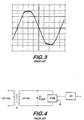
- RMS voltage of the AC line Another condition that can cause intensity variations and/or flickering is changes in the RMS voltage of the AC line. Changes in the RMS voltage of the AC line can be caused by the presence of harmonics of the AC fundamental on the AC line; the presence of these harmonics changes the shape of the AC line voltage waveform from a pure sinusoid to, e.g., a generally sinusoidal waveform having flattened peaks, rather than round peaks. See Figure 3. Changes in the RMS voltage of the AC line will cause intensity changes in the lighting load because such changes result in variations of the total power delivered to the load, irrespective of when the zero crossings occur.
- the prior art has failed to recognize that the conditions of noise/distortion on the AC line, on the one hand, and frequency variation of the AC line, on the other hand, may be simultaneously and/or alternatively present.
- the prior art has also failed to recognize that, in addition to the presence of these conditions, the condition of changing RMS voltage may also be simultaneously and/or alternatively present. To make matters worse, all of these conditions may be variably and intermittently present on the AC line, and these and other line conditions may be constantly changing. A condition that is present at one moment may be gone or replaced by another at the next moment; one combination of conditions may exist at one moment and be replaced by another combination at the next moment; and/or all or none of these conditions may exist at any given time.
- the condition of the AC line can be extremely dynamic. No prior art has attempted to address the problem of detecting zero crossings in the AC line under combinations of these conditions, in part, because the prior art has not recognized this dynamic nature of the AC line.
- the applicants hereof have not only recognized the dynamic nature of the AC line, but have also recognized why the prior art is incapable of addressing all of these conditions.
- the applicants hereof have recognized that conventional techniques for detecting zero crossings in the presence of noise/distortion are inconsistent with conventional techniques for detecting zero crossings in an AC line of unstable frequency, and that the prior art solutions to these problems conflict.
- the conditions of noise and distortion suggest that the AC line be integrated over a number of cycles, and therefore over a period of time, as is done when using a phase locked loop.
- the conditions of frequency changes and changes in RMS voltage suggest an instantaneous analysis of the AC line and an instantaneous response to any frequency or RMS voltage change.
- invoking a time delay and instantaneous analysis and response are conflicting solutions.
- the PLL method that is effective in a noisy environment is ineffective when the AC line frequency is unstable, because the PLL effectively employs an integration technique and frequency changes in the AC line can result in a temporary phase shift between the internally generated signal and the AC line.
- the PLL will adjust the phase of the internal signal to create substantial coincidence with the AC line, but during the adjustment time, the conduction angle of the thyristor will vary and may be manifested as slow intensity variations in the lighting load. This condition can be aggravated if the magnitude and/or rate of frequency variation of the AC line is greater than the error correction rate of the PLL, because the PLL may then be unable to track the AC line due to timing limits in the software.
- phase difference between the AC line and the internal signal will become great, and the intensity of the light source may vary significantly. Any time there is a substantial difference between the AC line zero cross and the internally generated signal of the PPL for a substantial period of time, visible changes in light will occur.
- the window detection method that is effective to detect zero crossing in an AC line of unstable frequency is ineffective in the presence of noise/distortion because, when the sample window is open, any zero crossing that occurs, whether due to noise, distortion or an actual zero crossing of the AC line, can be taken as the actual zero crossing of the AC line.
- This type of system does not adequately distinguish noise and distortion from actual zero crossings, and can possibly aggravate flickering/intensity variation problems caused by false detection of zero crossings due to noise/distortion.
- Some prior art systems gate the thyristor at regular periodic intervals, based on a selected dimming level, on the assumption that there will be no change in the timing of the zero crossings of the AC fundamental, or in the RMS voltage of the AC line after the thyristor has begun conducting. They are designed to deliver what is assumed will be a fixed amount of power once conduction begins. In these systems, the problems caused by frequency changes and changes in the RMS voltage of the AC line can be exaggerated. For example, in a given cycle, both the frequency of the AC line may change (causing a change in the time between zero crossings), and, the RMS voltage of the AC line may change during conduction. Since, once fired, the thyristor will continue to conduct until the next zero crossing occurs, the RMS power delivered to the load can vary substantially relative to a preceding or succeeding cycle.
- the integration time of the PLL is made sufficiently large to avoid the effects of AC line noise, frequency variations as small as 0.2% can be visible, and in some locations, especially in some less industrialized countries, the frequency of the AC line supplied by the electric company can change substantially more than this over very short periods of time.
- Software can be employed in a dimming system to analyze the AC fundamental and address one or more of the above conditions, but a software based system can cause other problematic conditions, such as aliasing on the AC line, due to interaction between the system's sample clock and the AC line. Aliasing occurs when the waveform is under-sampled.
- the prior art also includes a dimming system, known as the N-Module, that has been made and sold by the assignee hereof.
- N-Module a dimming system
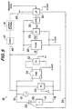
- a simplified diagram of a portion of the N-module is shown in Figure 4.
- a transformer T1 steps down 120VAC to 24VAC.
- a 2.2uF capacitor C1 placed across the output of T1, and before the full wave bridge rectifier (FWB), combines with the inherent leakage inductance of T1 to form an LC filter that reduces or eliminates frequencies above about 1.6 kHz.
- the filtered signal is supplied to the FWB, and the full wave rectified output of the FWB is analyzed for zero crossings by a zero crossing detector ZC.
- the output of ZC is then used for dimming purposes.
- the applicants hereof have determined that a solution to the dynamic problem discussed above requires a system that has both a fast response (for dealing with frequency variations in the AC line) and a narrow bandwidth (for eliminating the effects of noise and distortion outside the range of the fundamental frequency).
- the present invention is directed to such a solution.
- the preferred embodiment of the present invention is described herein in the context of a dimming system for a lighting load, but is not limited thereto, except as may be set forth expressly in the appended claims.
- the present invention has application to any AC controller that employs a phase control technique for control of load power, i.e., a system where a controllably conductive device is either turned on or off based on a length of time after detection of a zero cross of the AC line, for example, a phase control or reverse phase control dimmer.
- the present invention is described herein in the context of a wall mountable dimmer switch, but has applicability to any dimming system, including, by way of example, dimming systems with panel mounted dimmers, and the present invention is directed to and encompasses all such systems.
- dimming system including, by way of example, dimming systems with panel mounted dimmers
- present invention is directed to and encompasses all such systems.
- the implementation of the present invention in such applications and systems will be readily apparent to those skilled in the art from the following description.
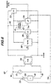
- Figures 5 - 7 there is shown in Figures 5 - 7 three different embodiments of a dimmer switch, such as a wall mountable dimmer switch, for a lighting load, each employing the present invention.
- Figures 5 and 6 illustrate the application of the invention in a typical three wire dimmer switch
- Figure 7 illustrates the application of the invention in a typical two wire dimmer switch.
- Each embodiment is characterized by a pass band or low pass filter that receives the AC line voltage either directly, in unrectified form ( Figures 5 and 7), or in full wave rectified form (Figure 6).
- the output of the filter is supplied to a zero cross detector and the output of the zero cross detector is supplied to a microprocessor (or an analog control circuit).
- the three wire dimmer switch 10 is connected to the AC source 12 and to the lighting load 14 by wires 16, 18, 20, in well known fashion.
- the load 14 is in series with a control device 22 that controls the RMS voltage applied to the load 14 in accordance with control signals supplied to a control electrode 24 by the microprocessor 26.
- the control device 22 is a controllably conductive device, such as a triac, MOSFET, IGBT, back to back SCR's, thyristors, etc., that receives trigger signals on a gate electrode 24 thereof from the microprocessor 26.
- the microprocessor 26 receives an input from a zero crossing detector 28 via an optocoupler 35 and also receives data indicative of the selected dimming level.
- Zero crossing detector 28 provides an output signal to the microprocessor 26 each time that a zero crossing of the input signal thereto is detected.
- Microprocessor 26 is programmed in well known fashion to set the desired dimming level in response to the zero crossing indications and the selected dimming level.
- a power supply 32 supplies necessary DC power to the microprocesssor 26.
- a power supply 33 on the AC side of the bridge 34 supplies necessary power to the filter 30, the zero cross detector 28, and the optocoupler 35.
- a full wave bridge rectifier 34 is employed to rectify the AC line.
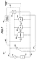
- the two wire dimming switch 10" is connected to one side of the load and to one side of the AC line by wires 16, 18 in well known fashion.
- the load 14 is in series with a thyristor 22 that controls the RMS voltage applied to the load 14 in accordance with control signals supplied to a control electrode 24 associated with a control device 22 by the microprocessor 26.
- the operation of the two wire dimmer switch is otherwise essentially as set forth above. Note optional "lightly filtered" circuit 41, explained hereinafter.
- the AC source voltage is provided to a low pass active filter 30, 30' and the output of the filter 30, 30' is supplied to a zero crossing detector 28.
- the AC line is filtered first, and the filter output is checked for the occurrence of zero crossings.
- the function of the filter 30, 30' is to substantially remove or attenuate frequency components of the AC line above the fundamental frequency (or above twice the fundamental frequency in certain cases), and to do so "quickly", i.e, with minimum, phase delay.
- the filter has a substantially flat frequency gain characteristic up to about the fundamental frequency (or up to about twice the fundamental frequency in certain cases) and a rapidly decreasing gain characteristic thereafter, and interposes a substantially linear phase delay (constant time delay) in the pass band to the fundamental frequency component.
- the output of the filter therefore is the AC fundamental component (or the second harmonic frequency of the AC fundamental component in certain cases), time delayed by a constant amount relative to the AC line, that is substantially free of noise and distortion.
- the output of the filter is the AC fundamental component (or the second harmonic frequency of the AC fundamental component) of the AC line, any fundamental frequency variations on the AC line will appear in the AC fundamental component (or the second harmonic frequency of the AC fundamental component) at the filter output. Therefore, the AC fundamental component (or the second harmonic frequency of the AC fundamental component) present at the filter output is a nearly ideal signal for zero crossing detection.
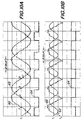
- Figure 10A is a plot showing the AC line entering the filter 30, line 60 of Figure 10A, and showing the output of the filter (AC fundamental), on line 62 of Figure 10A.
- Line 64 of Figure 10A shows the output of the zero crossing detector 28, where rising edges are indicative of zero crosses of the AC fundamental, line 62.
- the plots shown are for a 50Hz line frequency, i.e., a 10msec half period.
- the plot of Figure 10A is applicable to embodiments of the invention where the filter 30 is on the AC side of the dimming circuit, e.g., Figure 5. It will be seen that, in the example of Figure 10A, the plot 62 of the output of the filter 30 is phase delayed relative to the AC line plot 60 by approximately 5msec.
- the total phase delay time is the filter delay time.
- the filter delay time is dependent on the cut off frequency selected. In the preferred embodiment, the cutoff frequency selected is 55Hz. This results in approximately a 5msec filter delay time.
- the microprocessor 26 processes the information about the zero crosses from point B' to point C'; this is less than 1 msec.
- the information about the zero crosses is used by the microprocessor 26 to determine the half period of the AC fundamental 62, which will be used in order to properly gate the thyristor.
- the microprocessor is programmed to attempt to maintain constant duty cycle. Constant duty cycle means that even if the AC line frequency changes (which will change the time between zero crosses), the amount of power output to the load will be held constant. In order to maintain constant power while the AC line frequency is changing, the amount of time after the zero cross that the thyristor is to be fired must be adjusted.
- the filter 30 is designed to remove or substantially attenuate frequency components of the AC line voltage waveform that are substantially equal to third harmonics and greater of the AC fundamental. Second order harmonics are not an issue on the AC line, and any noise and distortion components are likely to be in a frequency range greater than the second harmonic frequency. Though an ideal filter would provide no phase delay, practical filter implementations always interpose some phase delay. In the preferred embodiment of the filter 30 of the present invention, the phase delay should not be more than half the period of the fundamental frequency (i.e., less than 180°) to ensure proper dimming function.
- phase delay should be no greater than about 135 ° to provide adequate time (within each half cycle of the AC line) for the microprocessor to compute a conduction angle and fire the thyristor well within this range of the half cycle.
- the requested dimming level is low enough, it is still possible to fire the thyristor at point C', or after point C' in the negative half cycle, with the zero cross information of the same half cycle. It is at these low light levels when the present invention is most beneficial. If the requested dimming level is such that the thyristor must be fired at a point prior to point C' in a half cycle, the system will wait until the next half cycle and will use the information from the previous half cycle. The system will use the most recent zero cross and period information available, which may be from an earlier half cycle of the same polarity.
- the microprocessor 26 will use information about the zero cross from the same half cycle in which the thyristor is to be fired. If the dimming system is fading from a high light level to a low light level, the microprocessor 26 will change from using information a half cycle old (i.e., from the previous half cycle) to using information from the same half cycle to fire the thyristor. Determining and programming such a transition, however, may complicate the coding of the microprocessor. For simplicity, information about the length of the half cycle from two prior half cycles may be used. Another reason for waiting until the next positive half cycle to use information about the previous positive half cycle is that the positive half cycle and the negative half cycle might not be symmetrical about zero volts. It is preferred to correct the dynamic problems during the same polarity of half cycle that the problem occurred, even if it is delayed by a full cycle.
- the filter 30 is coupled to receive the AC line 12 in unrectified form.
- the filter 30 is on the AC side of the circuit.
- the output of the filter 30 is supplied to zero crossing detector 28 as above described. Since the filter receives the AC line in unrectified form, i.e., the filter 30 receives the AC line at the fundamental frequency of 50/60 Hz, the criteria of an embodiment of the present invention may require that the gain characteristic of the filter be substantially flat up to about the fundamental frequency of 50/60 Hz, but this flatness is not critical to the overall operation of the invention.
- the filter 30' (which is substantially identical to filter 30, except as described hereafter) is coupled to receive the output of the full wave bridge rectifier 34.
- the filter 30' is on the DC side of the circuit, and receives the AC line in full wave rectified form rather than in unrectified form as in Figure 5.
- the filter thus receives the AC line at twice the frequency of the AC line 12 (and at twice the frequency of the filter 30 of Figure 5).
- the criteria of an embodiment of the present invention may require that the gain characteristic of the filter be substantially flat up to about the twice the fundamental frequency of 50/60 Hz, i.e., that it be substantially flat up to about 100/120 Hz, although, again, this flatness is not critical to the overall operation of the invention.
- the dimmer switch 10' of Figure 6 is otherwise identical to that of Figure 5.
- Figure 10B is a plot showing the full wave rectified AC line 60' and the recovered AC fundamental 62, i.e., the output of filter 30', for embodiments of the invention where the filter 30' is on the DC side of the dimming circuit, e.g., such as in the embodiment of Figure 6. Note the phase delay between the two waveforms.
- the phase delay of output waveform 62 from input waveform 60' is due to two components, a 90° phase shift caused by the full wave rectification, i.e., 2.5msec for a 50Hz supply and a 3msec phase delay through filter 30', which has a comer frequency of 111Hz, for a total phase delay of approximately 5.5msec.
- the filter 30 is disposed across the thyristor 22, and therefore receives the AC line in unrectified form, and the preceding discussion of Figure 5 is therefore applicable.
- the voltage across the thyristor 22 is the only available signal. For each half cycle of AC line voltage, the voltage across the thyristor 22 begins at zero and follows the incoming AC line. When the thyristor is gated on, the voltage across the thyristor 22 collapses to the forward voltage drop of the thyristor (typically 1.5 volts). The voltage remains at the forward voltage drop until the end of the half cycle.
- the signal across the thyristor 22 is available for the control circuitry to interpret and use for controlling the thyristor 22, as well as ancillary circuitry.
- the signal across the thyristor 22 always contains some component of fundamental line voltage.
- the signal also contains a varying component of harmonics of the fundamental. This varying component of harmonics changes with light level setting as well as with incoming power line quality.
- gating of a thyristor in an electronic dimmer requires a steady zero cross reference; this is also true for two wire dimmers. Since the zero cross filter previously described has the characteristic of finding the fundamental in the presence of distorted waveforms, it is well suited for finding the fundamental remaining in the voltage across the thyristor 22'.
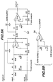
- FIG. 8A A four pole Bessel filter has been found to provide the desired results discussed above.
- One preferred implementation of a four pole Bessel filter is illustrated in Figure 8A.
- the implementation of Figure 8A has particular application to the embodiments of Figures 5, 6 and 7 since, as described below, its gain and falloff characteristics have been designed to meet the criteria discussed above in connection with Figure 6, namely a phase delay of no more than 135° at 120Hz. (Implementation of a similar filter to meet the criteria of Figures 5 and 7 is straightforward.)
- THE ART OF ELECTRONICS by Paul Horowitz and Winfield Hill, second edition (1991), Chapter 5 (Active Filters and Oscillators), pp. 272-275 fully describes active filter design and design criteria, including design of Bessel filters.
- Figure 8B illustrates one embodiment of a zero crossing detector that may be employed in connection with the present invention.
- IC1 is a LM324N, as manufactured by SGS Thomson.
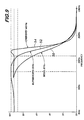
- Figure 9 illustrates the gain characteristic of the Bessel filter of Figure 8A (curve 50) and also illustrates gain characteristics of a Butterworth filter (curve 52) and a Chebyshev filter (curve 54) designed to provide about 135° phase delay at 120Hz, as may be used with the embodiment of Figure 6.
- the Bessel filter of Figure 8A has a corner frequency of about 111 Hz and has (relative to the Butterworth and Chebyshev filters) a shallow gain rolloff such that the filter has no appreciable gain (less than 20%) above 300 Hz.
- the corner frequency would preferably be about 55 Hz and the rolloff would be such that the filter has no appreciable gain above about 150 Hz.
- a relatively shallow rolloff such as shown by curve 50 for the disclosed Bessel filter, provides the most frequency attenuation with a constant phase delay, and also provides the most frequency attenuation in the portion of the frequency spectrum of most importance, i.e., in the first few harmonics of the fundamental.
- a Bessel filter is preferred, but is not necessary, as the filter choice, since a Bessel filter is simpler to design and implement, and because it has a relatively constant phase delay, regardless of the AC line frequency.
- the filter output (recovered AC fundamental on line 62), or second harmonic frequency of the AC fundamental on line 62') is substantially cleaner than the incoming AC line.
- Figures 11A and 11B are spectral plots of an exemplary AC line into, and the recovered signal out of, the filter 30, respectively. It will be seen that the frequency content of the recovered signal above the fundamental frequency is substantially reduced relative to that of the AC line.
- Figure 12 is a self-explanatory flow diagram for the microprocessor 26 for maintaining constant duty cycle.
- the microprocessor captures the most recent zero cross (T B ) and the previous zero cross (T A ) of the output of the filter 30, 30' and then calculates the half cycle period.
- the end user is allowed to set the maximum high end and the minimum low end. By adjusting the high end, the end user can either reduce the maximum voltage and extend incandescent bulb life or increase the maximum voltage and obtain more light output.
- the microprocessor calculates the high end as a function of the period. By adjusting the low end, the end user can properly set the minimum voltage which is very important with fluorescent loads.
- the microprocessor calculates the low end as a function of the period.
- the high end adjustment range is 50% to 95% (K), with the setting typically at about 95% for incandescent loads and at about 70% for fluorescent loads.
- the low end adjustment range is 5% to 49% (M), with the setting typically at about 5% for incandescent loads and at about 30% for fluorescent loads.
- M 5% to 49%
- the system allows the end user to set a dimmer to a light level by selecting a value from a digital display.
- the microprocessor then fires the thyristor at time T B - phase delay + Fire using a phase delay value retrieved from memory at 207.
- This phase delay value is the phase delay, ⁇ delay, shown in Figures 10A and 10B.
- a nominal value for the phase delay of an ideal filter e.g., 5msec, can be stored in microprocessor 26 when the system is manufactured. This nominal value can be replaced with a value which reflects the measured actual phase delay of the specific filter 30, 30' connected to the microprocessor 26 as described below in connection with Figure 13.
- the microprocessor then waits for the next zero cross, and the sequence begins again at 200.
- Light filtering can be performed by a simple (usually passive) low-pass filter, for example a single resistor-capacitor stage, whose cutoff frequency is low enough to remove as much as possible of the line noise, but, high enough that the phase delay it introduces at the fundamental frequency is small enough that variation of that phase delay with variation with component tolerances (even with low-precision components) is insignificant.
- the light filtering can be performed by software routines incorporated into microprocessor 26.
- Figure 13 shows a filter phase delay compensation flowchart.
- the system monitors the lightly filtered AC line 42 and measures the phase delay between it and the "heavily filtered" AC fundamental or second harmonic frequency of the AC fundamental output from the filter 30, 30'.
- Heavy filtering can be performed by a low-pass filter (such as the active low pass filter described above) whose cutoff frequency is close to the fundamental line frequency (or twice that frequency, when the input to the filter is a full-wave rectified waveform), or a narrow-band pass filter.
- a low-pass filter such as the active low pass filter described above
- the microprocessor 26 can derive the phase delay of the actual filter 30, 30' from the difference between the heavily filtered and lightly filtered inputs. Even if the lightly filtered line 42 is unstable due to line noise, the microprocessor 26 can average this value over many line cycles to minimize the influence of the noise. Thus, the microprocessor 26 can compensate for the phase delay.
- Figure 13 shows a flow chart for implementing the zero cross filter delay compensation system shown in dashed lines in Figures 5,6 and 7.
- the microprocessor captures a zero cross from the lightly filtered line 42 into the microprocessor 26 as T1.
- the microprocessor captures a zero cross from the heavily filtered line output from the filter 30, 30' into the microprocessor 26 as T2.
- the microprocessor calculates the difference between T1 and T2 and stores it as ⁇ Tn.
- the microprocessor takes an average of the last K samples of ⁇ Tn and stores this as ⁇ Tavg, where K is an empirically chosen value from 10 to 10,000.
- the microprocessor stores ⁇ Tavg as the phase delay value to be retrieved at step 207 of the routine illustrated in Figure 12 in place of any previously stored value.
- the routine illustrated in the flow chart of Figure 13 is performed periodically to update the stored value of the phase delay. It is typically done whenever power is applied to the system and then at least once per day. However, it can be performed as frequently as many times per second.
- a band pass filter a circuit containing passive circuit elements, a switched capacitor filter or a software implementation of the analog hardware filter disclosed herein may be employed, and such substitution is within the scope of the present invention.
- a system employing digital signal processing (DSP) with a high speed analog to digital converter (i.e., greater than 20 kHz) can sample and then recreate the incoming AC line.
- DSP digital signal processing
- the system can "filter” out any frequency above the fundamental. This could be used instead of the filter described above.
- the remaining fundamental frequency can then be fed into the zero cross detector and then into the microprocessor in order to properly fire the thyristor, as was previously described.
- the DSP, zero cross detector and microprocessor can be incorporated into one device.
Abstract
Description
Claims (20)
- A load control system, connectable to an AC line (16) and a load (14), for controlling the power delivered from the AC line to the load, wherein the AC line has a fundamental component with a fundamental frequency, the system comprising:-characterised in that said filter (30, 30') comprises an active filter and interposes a substantially linear phase delay relative to the AC line and has a frequency characteristic such that substantially a selected one of the AC fundamental or the second harmonic frequency of the AC fundamental component is passed and such that third order and greater harmonics of the fundamental frequency are substantially attenuated.a filter (30, 30') having a frequency characteristic such that high frequencies relative to said fundamental frequency are substantially attenuated;a zero cross detector (28) coupled to receive an output of the filter and providing an indication of zero crossings thereof;a controllably conductive device (22) connected in series to the AC line and the load; anda control circuit (26) generating trigger signals in response to the indications provided by the zero cross detector (28) for rendering the controllably conductive device (22) conductive for at least a portion of a cycle of the AC line;
- A load control system according to claim 1 wherein the filter interposes a substantially linear phase delay of less than one-half of a period of the fundamental frequency.
- A load control system according to claim 1 or 2
wherein the filter is coupled to receive an unrectified AC line and has a substantially flat frequency gain characteristic up to about the fundamental frequency and a rapidly decreasing gain characteristic thereafter, the filtered signal being a substantial representation of the AC fundamental. - A load control system according to claim 1 or 2 further comprising:-
a full wave bridge rectifier (34) for providing a full wave rectified AC line;
wherein the filter is coupled to receive the full wave rectified AC line and has a substantially flat frequency gain characteristic up to about twice the fundamental frequency and a rapidly decreasing gain characteristic thereafter, the filtered signal being a substantial representation of the second harmonic frequency of the AC fundamental. - A load control system according to claim 4 wherein no optical coupling device is employed for detecting zero crossings.
- A load control system according to any one of claims 1 to 3 wherein the fundamental frequency is in the range of 50-60Hz and the filter is a Bessel filter having a corner frequency of about 55Hz, a phase delay of about 135° at the fundamental frequency and no substantial frequency gain after about 150Hz.
- A load control system according to any one of claims 1,2 4 or 5 wherein the fundamental frequency is in the range of 50-60Hz and the filter is a Bessel filter having a corner frequency of about 111 Hz, a phase delay of about 135° at the fundamental frequency and no substantial frequency gain after about 300Hz.
- A load control system according to claim 6 or 7 wherein the Bessel filter comprises an analog hardware filter.
- A load control system according to any preceding claim wherein the filter is an active filter.
- A load control system according to any one of claims 1 to 5 wherein the filter is a band pass filter.
- A load control system according to any one of claims 1 to 5 wherein the filter is a passive filter.
- A load control system according to any one of claims 1 to 5 wherein the filter is a switched capacitor filter.
- A load control system according to any one of claims 1 to 5 wherein the filter is a software filter.
- A load control system according to any one of claims 1 to 5 wherein the filter comprises a digital signal processor.
- A load control system according to any preceding claim wherein the filter is disposed across at least one of the controllably conductive device and the load.
- A load control system according to any preceding claim wherein the control circuit comprises a microprocessor providing the control signals according to the zero crossing indications and a desired power level set by a user.
- A load control system according to claims 16 wherein the microprocessor measures an actual delay of the filtered signal based upon the zero crossing indications and an input of one of an unfiltered and lightly filtered (41) AC line and, based on the measured actual phase delay, and adjusts the timing of the control signals to compensate for the actual phase delay through the filter.
- A load control system according to any preceding claim wherein the system comprises one of a two wire wall mountable dimmer switch, a three wire wall mountable dimming switch, and a dimming panel.
- A load control system according to any preceding claim wherein the controllably conductive device comprises a thyristor.
- A load control system according to any one of claims 1 to 18 wherein the controllably conductive device comprises a triac,
Applications Claiming Priority (3)
| Application Number | Priority Date | Filing Date | Title |
|---|---|---|---|
| US942833 | 1997-10-02 | ||
| US08/942,833 US6091205A (en) | 1997-10-02 | 1997-10-02 | Phase controlled dimming system with active filter for preventing flickering and undesired intensity changes |
| PCT/US1998/019842 WO1999018651A1 (en) | 1997-10-02 | 1998-09-24 | Phase controlled dimming system with active filter for preventing flickering and undesired intensity changes |
Publications (2)
| Publication Number | Publication Date |
|---|---|
| EP1018208A1 EP1018208A1 (en) | 2000-07-12 |
| EP1018208B1 true EP1018208B1 (en) | 2003-03-12 |
Family
ID=25478665
Family Applications (1)
| Application Number | Title | Priority Date | Filing Date |
|---|---|---|---|
| EP98948456A Revoked EP1018208B1 (en) | 1997-10-02 | 1998-09-24 | Phase controlled dimming system with active filter for preventing flickering and undesired intensity changes |
Country Status (11)
| Country | Link |
|---|---|
| US (2) | US6091205A (en) |
| EP (1) | EP1018208B1 (en) |
| JP (2) | JP2001519639A (en) |
| AT (1) | ATE234529T1 (en) |
| AU (1) | AU738147B2 (en) |
| CA (1) | CA2305536C (en) |
| DE (1) | DE69812133T2 (en) |
| ES (1) | ES2194354T3 (en) |
| HK (1) | HK1031159A1 (en) |
| IL (1) | IL135692A (en) |
| WO (1) | WO1999018651A1 (en) |
Families Citing this family (123)
| Publication number | Priority date | Publication date | Assignee | Title |
|---|---|---|---|---|
| FR2802360B1 (en) * | 1999-12-14 | 2002-03-01 | Legrand Sa | METHOD AND DEVICE FOR ELECTRIC POWER SUPPLY OF A LOAD BY A DRIVE HAS AT LEAST ONE SWITCH CONTROLLED |
| US6660948B2 (en) * | 2001-02-28 | 2003-12-09 | Vip Investments Ltd. | Switch matrix |
| US6724157B2 (en) | 2001-11-14 | 2004-04-20 | Astral Communications Inc. | Energy savings device and method for a resistive and/or an inductive load |
| US6836080B2 (en) * | 2001-11-14 | 2004-12-28 | Astral Communications, Inc. | Energy savings device and method for a resistive and/or an inductive load and/or a capacitive load |
| DE10203892B4 (en) * | 2002-01-31 | 2004-01-29 | Infineon Technologies Ag | Method for generating a signal pulse sequence with a predetermined stable fundamental frequency |
| US7327805B2 (en) * | 2002-02-28 | 2008-02-05 | Tsi Telsys, Inc. | Device, apparatus and method for receiving data transmissions having different data rates |
| AUPS131202A0 (en) * | 2002-03-25 | 2002-05-09 | Clipsal Integrated Systems Pty Ltd | Circuit arrangement for power control |
| SE0302191D0 (en) * | 2003-03-10 | 2003-08-11 | Staffan Gunnarsson | Transponder with infrared technology |
| US7012518B2 (en) * | 2003-04-18 | 2006-03-14 | Cooper Wiring Devices, Inc. | Dimmer control system with two-way master-remote communication |
| US6987449B2 (en) * | 2003-04-18 | 2006-01-17 | Cooper Wiring Devices, Inc. | Dimmer control system with tandem power supplies |
| KR100512962B1 (en) * | 2003-05-19 | 2005-09-07 | 삼성전자주식회사 | A controlling apparatus and a controlling method of heater lamp provided with pulse signal corresponding to detected input AC voltage |
| US7755506B1 (en) | 2003-09-03 | 2010-07-13 | Legrand Home Systems, Inc. | Automation and theater control system |
| US8154841B2 (en) * | 2003-09-03 | 2012-04-10 | Legrand Home Systems, Inc. | Current zero cross switching relay module using a voltage monitor |
| US6906477B2 (en) * | 2003-10-14 | 2005-06-14 | Astral Communications, Inc. | Linear control device for controlling a resistive and/or an inductive and/or a capacitive load |
| US7183670B2 (en) * | 2004-01-29 | 2007-02-27 | Me Electronic Products Limited | Power supply for electronic switch |
| US7834856B2 (en) | 2004-04-30 | 2010-11-16 | Leviton Manufacturing Co., Inc. | Capacitive sense toggle touch dimmer |
| US7259524B2 (en) * | 2004-06-10 | 2007-08-21 | Lutron Electronics Co., Inc. | Apparatus and methods for regulating delivery of electrical energy |
| JP4379235B2 (en) * | 2004-07-14 | 2009-12-09 | パナソニック電工株式会社 | Light control device |
| US7440246B2 (en) * | 2004-10-15 | 2008-10-21 | Leviton Manufacturing Co., Inc. | Circuit interrupting apparatus with remote test and reset activation |
| US20090212967A1 (en) * | 2004-10-15 | 2009-08-27 | Leviton Manufacturing Company, Inc | Circuit Interrupting System with Remote Test And Reset Activation |
| US7482758B2 (en) * | 2005-03-03 | 2009-01-27 | Leviton Manufacturing Co., Inc. | Magnetic low voltage dimmer |
| US8892913B2 (en) | 2005-06-30 | 2014-11-18 | Lutron Electronics Co., Inc. | Load control device having a low-power mode |
| DE102005030634A1 (en) * | 2005-06-30 | 2007-01-04 | BSH Bosch und Siemens Hausgeräte GmbH | Circuit arrangement for determining zero crossings of an alternating voltage |
| CA2613242C (en) | 2005-06-30 | 2012-12-11 | Lutron Electronics Co., Inc. | Dimmer having a microprocessor-controlled power supply |
| US7778262B2 (en) | 2005-09-07 | 2010-08-17 | Vantage Controls, Inc. | Radio frequency multiple protocol bridge |
| US8386661B2 (en) * | 2005-11-18 | 2013-02-26 | Leviton Manufacturing Co., Inc. | Communication network for controlling devices |
| WO2007068042A1 (en) * | 2005-12-12 | 2007-06-21 | Clipsal Australia Pty Ltd | Current zero crossing detector in a dimmer circuit |
| DE102006005289A1 (en) | 2006-02-06 | 2007-08-30 | Siemens Ag | Dimmer circuit with zero crossing correction |
| EP2006362A4 (en) * | 2006-03-30 | 2010-11-10 | Mitsui Shipbuilding Eng | Process for producing gas hydrate pellet |
| US7566987B2 (en) * | 2006-09-14 | 2009-07-28 | Lutron Electronics Co., Inc. | Method of powering up a plurality of loads in sequence |
| US7781919B2 (en) | 2006-09-14 | 2010-08-24 | Lutron Electronics Co., Inc. | Method of controlling a load control module as part of a startup sequence |
| US7741732B2 (en) * | 2006-09-14 | 2010-06-22 | Lutron Electronics Co., Inc. | Method of configuring a startup sequence of a load control system |
| US7538285B2 (en) | 2007-03-30 | 2009-05-26 | Leviton Manufacturing Company, Inc. | Electrical control device |
| US7756556B2 (en) * | 2006-11-14 | 2010-07-13 | Leviton Manufacturing Company, Inc. | RF antenna integrated into a control device installed into a wall switch box |
| US20080309379A1 (en) * | 2007-03-02 | 2008-12-18 | Carroll Sean C | Zero crossing circuit |
| US8018171B1 (en) * | 2007-03-12 | 2011-09-13 | Cirrus Logic, Inc. | Multi-function duty cycle modifier |
| US7288902B1 (en) | 2007-03-12 | 2007-10-30 | Cirrus Logic, Inc. | Color variations in a dimmable lighting device with stable color temperature light sources |
| US7667408B2 (en) | 2007-03-12 | 2010-02-23 | Cirrus Logic, Inc. | Lighting system with lighting dimmer output mapping |
| US7969100B2 (en) * | 2007-05-17 | 2011-06-28 | Liberty Hardware Manufacturing Corp. | Bulb type detector for dimmer circuit and inventive resistance and short circuit detection |
| US7855518B2 (en) * | 2007-06-19 | 2010-12-21 | Masco Corporation | Dimming algorithms based upon light bulb type |
| US7985937B2 (en) * | 2007-07-18 | 2011-07-26 | Leviton Manufacturing Co., Ltd. | Dimmer switch |
| US20100101924A1 (en) * | 2007-07-18 | 2010-04-29 | Leviton Manufacturing Co., Inc. | Switching device |
| US20090028372A1 (en) * | 2007-07-23 | 2009-01-29 | Leviton Manufacturing Co., Inc. | Light fixture with sound capability |
| US8468165B2 (en) * | 2007-12-02 | 2013-06-18 | Leviton Manufacturing Company, Inc. | Method for discovering network of home or building control devices |
| US7609007B1 (en) | 2008-02-26 | 2009-10-27 | Creston Electronics, Inc. | Dimmer adaptable to either two or three active wires |
| US7928663B1 (en) | 2008-02-26 | 2011-04-19 | Crestron Electronics Inc. | Lighting dimmer adaptable to four wiring configurations |
| US7956694B1 (en) | 2008-05-12 | 2011-06-07 | Wilson Jeffrey D | Phase controlled dimmer using a narrow band quadrature demodulator |
| US8360669B2 (en) * | 2008-06-23 | 2013-01-29 | Silverbrook Research Pty Ltd | Retractable electronic pen with sensing arrangement |
| US8482391B2 (en) * | 2008-11-19 | 2013-07-09 | System General Corp. | Wall control interface with phase modulation and detection for power management |
| WO2010076720A1 (en) | 2008-12-30 | 2010-07-08 | Koninklijke Philips Electronics N.V. | Electronic circuit for driving a fluorescent lamp and lighting application |
| US8149591B2 (en) | 2009-02-20 | 2012-04-03 | Creston Electronics Inc. | Wall box dimmer |
| US8547035B2 (en) * | 2009-07-15 | 2013-10-01 | Crestron Electronics Inc. | Dimmer adaptable to either two or three active wires |
| JP2011036040A (en) * | 2009-07-31 | 2011-02-17 | Renesas Electronics Corp | System interconnection system and system interconnection method |
| JP2011039648A (en) * | 2009-08-07 | 2011-02-24 | Rkc Instrument Inc | Ac power control device |
| US9155174B2 (en) | 2009-09-30 | 2015-10-06 | Cirrus Logic, Inc. | Phase control dimming compatible lighting systems |
| US9143141B2 (en) * | 2009-10-05 | 2015-09-22 | Siemens Industry, Inc. | Apparatus and methods for power quality measurement |
| US8957662B2 (en) * | 2009-11-25 | 2015-02-17 | Lutron Electronics Co., Inc. | Load control device for high-efficiency loads |
| USD651578S1 (en) | 2010-02-01 | 2012-01-03 | Crestron Electronics Inc. | Wall mounted button panel |
| USD651579S1 (en) | 2010-02-01 | 2012-01-03 | Crestron Electronics Inc. | Wall mounted button panel |
| USD678850S1 (en) | 2011-06-13 | 2013-03-26 | Crestron Electronics Inc. | Wall mounted button panel |
| USD651575S1 (en) | 2010-02-01 | 2012-01-03 | Crestron Electronics Inc. | Wall mounted button panel |
| USD651571S1 (en) | 2010-02-01 | 2012-01-03 | Crestron Electronics Inc. | Wall mounted button panel |
| USD651577S1 (en) | 2010-02-01 | 2012-01-03 | Crestron Electronics Inc. | Wall mounted button panel with split buttons |
| USD651985S1 (en) | 2010-02-01 | 2012-01-10 | Crestron Electronics Inc. | Wall mounted button panel with split buttons |
| USD651983S1 (en) | 2010-02-01 | 2012-01-10 | Creston Electronics Inc. | Wall mounted button panel |
| USD651576S1 (en) | 2010-02-01 | 2012-01-03 | Crestron Electronics Inc. | Wall mounted button panel |
| USD678222S1 (en) | 2011-06-10 | 2013-03-19 | Crestron Electronics Inc. | Wall mounted button panel |
| USD651984S1 (en) | 2010-02-01 | 2012-01-10 | Crestron Electronics Inc. | Wall mounted button panel |
| USD651572S1 (en) | 2010-02-01 | 2012-01-03 | Crestron Electroncs Inc. | Wall mounted button panel |
| USD651573S1 (en) | 2010-02-01 | 2012-01-03 | Crestron Electronics Inc. | Wall mounted button panel |
| USD651574S1 (en) | 2010-02-01 | 2012-01-03 | Crestron Electronics Inc. | Wall mounted button panel |
| USD678851S1 (en) | 2011-06-14 | 2013-03-26 | Crestron Electronics Inc. | Wall mounted button panel |
| US8553439B2 (en) * | 2010-02-09 | 2013-10-08 | Power Integrations, Inc. | Method and apparatus for determining zero-crossing of an AC input voltage to a power supply |
| USD651986S1 (en) | 2010-02-19 | 2012-01-10 | Crestron Electronics Inc. | Wall mounted button panel with split buttons |
| USD651580S1 (en) | 2010-02-19 | 2012-01-03 | Crestron Electronics Inc. | Wall mounted button panel with split buttons |
| USD652806S1 (en) | 2010-02-19 | 2012-01-24 | Crestron Electronics Inc. | Wall mounted button panel with split buttons |
| USD653220S1 (en) | 2010-02-19 | 2012-01-31 | Crestron Electronics Inc. | Wall mounted button panel with split buttons |
| USD657319S1 (en) | 2010-02-19 | 2012-04-10 | Crestron Electronics Inc. | Wall mounted button panel with split buttons |
| USD652805S1 (en) | 2010-02-19 | 2012-01-24 | Crestron Electronics Inc. | Wall mounted button panel with split buttons |
| JP5785611B2 (en) * | 2010-05-17 | 2015-09-30 | コーニンクレッカ フィリップス エヌ ヴェ | Method and apparatus for detecting and correcting improper dimmer operation |
| US8716957B2 (en) * | 2010-07-30 | 2014-05-06 | Cirrus Logic, Inc. | Powering high-efficiency lighting devices from a triac-based dimmer |
| US8536799B1 (en) | 2010-07-30 | 2013-09-17 | Cirrus Logic, Inc. | Dimmer detection |
| US8941316B2 (en) | 2010-08-17 | 2015-01-27 | Cirrus Logic, Inc. | Duty factor probing of a triac-based dimmer |
| US8729811B2 (en) | 2010-07-30 | 2014-05-20 | Cirrus Logic, Inc. | Dimming multiple lighting devices by alternating energy transfer from a magnetic storage element |
| US9307601B2 (en) | 2010-08-17 | 2016-04-05 | Koninklijke Philips N.V. | Input voltage sensing for a switching power converter and a triac-based dimmer |
| WO2012027507A2 (en) | 2010-08-24 | 2012-03-01 | Cirrus Logic, Inc. | Multi-mode dimmer interfacing including attach state control |
| BE1019523A5 (en) * | 2010-09-30 | 2012-08-07 | Niko Nv | ZERO TRANSACTION DETECTOR, USE OF SUCH DETECTOR AND DIMMER INCLUDING SUCH DETECTOR. |
| WO2012061769A2 (en) | 2010-11-04 | 2012-05-10 | Cirrus Logic, Inc. | Controlled power dissipation in a switch path in a lighting system |
| WO2012061774A2 (en) | 2010-11-04 | 2012-05-10 | Cirrus Logic, Inc. | Controlled energy dissipation in a switching power converter |
| PL2681969T3 (en) | 2010-11-16 | 2019-11-29 | Signify Holding Bv | Trailing edge dimmer compatibility with dimmer high resistance prediction |
| US9025347B2 (en) | 2010-12-16 | 2015-05-05 | Cirrus Logic, Inc. | Switching parameter based discontinuous mode-critical conduction mode transition |
| USD702195S1 (en) | 2011-06-16 | 2014-04-08 | Crestron Electronics Inc. | Wall mounted button panel |
| WO2013003673A1 (en) | 2011-06-30 | 2013-01-03 | Cirrus Logic, Inc. | Transformer-isolated led lighting circuit with secondary-side dimming control |
| WO2013090852A2 (en) | 2011-12-14 | 2013-06-20 | Cirrus Logic, Inc. | Adaptive current control timing and responsive current control for interfacing with a dimmer |
| EP2820919A1 (en) | 2012-02-29 | 2015-01-07 | Cirrus Logic, Inc. | Mixed load current compensation for led lighting |
| AU2013201587B2 (en) * | 2012-03-27 | 2016-07-14 | Hendon Semiconductors Pty Ltd | An electronic control system for operating a street lamp |
| US9489005B2 (en) | 2012-03-28 | 2016-11-08 | Lutron Electronics Co., Inc. | Method and apparatus for phase-controlling a load |
| US9130373B2 (en) | 2012-04-19 | 2015-09-08 | Pass & Seymour, Inc. | Universal power control device |
| US10340692B2 (en) | 2012-04-19 | 2019-07-02 | Pass & Seymour, Inc. | Universal power control device |
| US9184661B2 (en) | 2012-08-27 | 2015-11-10 | Cirrus Logic, Inc. | Power conversion with controlled capacitance charging including attach state control |
| US9596741B2 (en) | 2012-09-05 | 2017-03-14 | Legrand North America, LLC | Dimming control including an adjustable output response |
| US9250669B2 (en) | 2012-09-14 | 2016-02-02 | Lutron Electronics Co., Inc. | Power measurement in a two-wire load control device |
| US9155162B2 (en) | 2012-09-14 | 2015-10-06 | Lutron Electronics Co., Inc. | Two-wire dimmer with improved zero-cross detection |
| US9093894B2 (en) | 2012-12-17 | 2015-07-28 | Greenmark Technology Inc. | Multiple-level power control system |
| KR101474078B1 (en) * | 2012-12-21 | 2014-12-17 | 삼성전기주식회사 | Dimming control apparatus, lighting driving apparatus and dimming control method |
| USD707637S1 (en) | 2013-01-03 | 2014-06-24 | Crestron Electronics Inc. | Wall mounted button panel with split buttons |
| USD702193S1 (en) | 2013-01-03 | 2014-04-08 | Crestron Electronics Inc. | Wall mounted button panel with split buttons |
| US9496844B1 (en) | 2013-01-25 | 2016-11-15 | Koninklijke Philips N.V. | Variable bandwidth filter for dimmer phase angle measurements |
| EP2974545A1 (en) | 2013-03-14 | 2016-01-20 | Koninklijke Philips N.V. | Controlled electronic system power dissipation via an auxiliary-power dissipation circuit |
| US9282598B2 (en) | 2013-03-15 | 2016-03-08 | Koninklijke Philips N.V. | System and method for learning dimmer characteristics |
| US9621062B2 (en) | 2014-03-07 | 2017-04-11 | Philips Lighting Holding B.V. | Dimmer output emulation with non-zero glue voltage |
| AU2015237427B2 (en) * | 2014-03-27 | 2017-09-07 | Daikin Industries, Ltd. | Power conversion device |
| US9996096B2 (en) | 2014-03-28 | 2018-06-12 | Pass & Seymour, Inc. | Power control device with calibration features |
| US9215772B2 (en) | 2014-04-17 | 2015-12-15 | Philips International B.V. | Systems and methods for minimizing power dissipation in a low-power lamp coupled to a trailing-edge dimmer |
| US9655219B2 (en) * | 2014-09-30 | 2017-05-16 | Chia-Teh Chen | On line automatic detection of the time phase of the threshold voltage of a lighting load and its application in lighting management |
| US10264643B1 (en) | 2018-05-09 | 2019-04-16 | Leviton Manufacturing Co., Inc. | Dual over-current protection for phase cut dimmer |
| US11464096B2 (en) | 2018-09-28 | 2022-10-04 | Leviton Manufacturing Co., Inc. | Dimmer with improved noise immunity |
| MX2021006231A (en) | 2018-11-30 | 2021-12-10 | Lutron Tech Co Llc | Load control device configured to operate in two-wire and three-wire modes. |
| CN109672343B (en) * | 2018-12-17 | 2020-12-18 | 华为技术有限公司 | Phase calibration circuit and method of receiving end and receiving end |
| US11903105B2 (en) | 2020-05-21 | 2024-02-13 | Leviton Manufacturing Co., Inc. | Prediction and recovery of zero-crossing information and selective control signal pulse duration |
| WO2021236174A1 (en) * | 2020-05-21 | 2021-11-25 | Leviton Manufacturing Co., Inc. | Switching control in electrical load controllers |
| WO2022221735A1 (en) | 2021-04-16 | 2022-10-20 | Lutron Technology Company Llc | Load control device having miswire detection |
| US11871493B2 (en) | 2021-06-04 | 2024-01-09 | Leviton Manufacturing Co., Inc. | Timing adjustments for accurate zero-crossing determination |
Family Cites Families (13)
| Publication number | Priority date | Publication date | Assignee | Title |
|---|---|---|---|---|
| US3990000A (en) * | 1975-07-10 | 1976-11-02 | Rca Corporation | Alternating current control system |
| JPS57206932A (en) * | 1981-06-15 | 1982-12-18 | Matsushita Electric Works Ltd | Phase controlling device |
| US5629607A (en) * | 1984-08-15 | 1997-05-13 | Callahan; Michael | Initializing controlled transition light dimmers |
| US4823069A (en) | 1984-08-15 | 1989-04-18 | Michael Callahan | Light dimmer for distributed use employing inductorless controlled transition phase control power stage |
| US4728866A (en) * | 1986-09-08 | 1988-03-01 | Lutron Electronics Co., Inc. | Power control system |
| US5099193A (en) * | 1987-07-30 | 1992-03-24 | Lutron Electronics Co., Inc. | Remotely controllable power control system |
| US4797802A (en) * | 1987-12-03 | 1989-01-10 | Sundstrand Corp. | Multiple phase rectifier with active filter for removing noise in triggering signals and digital phase shift compensator for phase shifting signal passed through |
| US5038081A (en) * | 1987-12-16 | 1991-08-06 | Lutron Electronics Co., Inc. | Reverse phase-controlled dimmer |
| US5264761A (en) * | 1991-09-12 | 1993-11-23 | Beacon Light Products, Inc. | Programmed control module for inductive coupling to a wall switch |
| US5268631A (en) * | 1991-11-06 | 1993-12-07 | Chicago Stage Equipment Co. | Power control system with improved phase control |
| GB2267788B (en) * | 1992-06-04 | 1997-01-29 | Strand Lighting Ltd | Dimming system, and dimmer therefor |
| US5430356A (en) * | 1993-10-05 | 1995-07-04 | Lutron Electronics Co., Inc. | Programmable lighting control system with normalized dimming for different light sources |
| US5650694A (en) * | 1995-03-31 | 1997-07-22 | Philips Electronics North America Corporation | Lamp controller with lamp status detection and safety circuitry |
-
1997
- 1997-10-02 US US08/942,833 patent/US6091205A/en not_active Expired - Lifetime
-
1998
- 1998-09-24 CA CA002305536A patent/CA2305536C/en not_active Expired - Lifetime
- 1998-09-24 AT AT98948456T patent/ATE234529T1/en not_active IP Right Cessation
- 1998-09-24 DE DE69812133T patent/DE69812133T2/en not_active Expired - Lifetime
- 1998-09-24 WO PCT/US1998/019842 patent/WO1999018651A1/en active IP Right Grant
- 1998-09-24 EP EP98948456A patent/EP1018208B1/en not_active Revoked
- 1998-09-24 ES ES98948456T patent/ES2194354T3/en not_active Expired - Lifetime
- 1998-09-24 AU AU95025/98A patent/AU738147B2/en not_active Ceased
- 1998-09-24 IL IL13569298A patent/IL135692A/en not_active IP Right Cessation
- 1998-09-24 JP JP2000515323A patent/JP2001519639A/en not_active Withdrawn
-
2000
- 2000-09-18 US US09/664,232 patent/US6380692B1/en not_active Expired - Lifetime
-
2001
- 2001-01-12 HK HK01100367A patent/HK1031159A1/en not_active IP Right Cessation
-
2007
- 2007-09-13 JP JP2007238444A patent/JP4272245B2/en not_active Expired - Lifetime
Also Published As
| Publication number | Publication date |
|---|---|
| ES2194354T3 (en) | 2003-11-16 |
| EP1018208A1 (en) | 2000-07-12 |
| DE69812133D1 (en) | 2003-04-17 |
| JP4272245B2 (en) | 2009-06-03 |
| AU9502598A (en) | 1999-04-27 |
| US6380692B1 (en) | 2002-04-30 |
| JP2001519639A (en) | 2001-10-23 |
| HK1031159A1 (en) | 2001-06-01 |
| CA2305536A1 (en) | 1999-04-15 |
| US6091205A (en) | 2000-07-18 |
| JP2008029197A (en) | 2008-02-07 |
| IL135692A (en) | 2004-12-15 |
| AU738147B2 (en) | 2001-09-13 |
| DE69812133T2 (en) | 2003-12-04 |
| CA2305536C (en) | 2007-03-13 |
| ATE234529T1 (en) | 2003-03-15 |
| WO1999018651A1 (en) | 1999-04-15 |
Similar Documents
| Publication | Publication Date | Title |
|---|---|---|
| EP1018208B1 (en) | Phase controlled dimming system with active filter for preventing flickering and undesired intensity changes | |
| US6407515B1 (en) | Power regulator employing a sinusoidal reference | |
| US20210282238A1 (en) | Two-wire dimmer with improved zero-cross detention | |
| CA2569996C (en) | Apparatus and methods for regulating delivery of electrical energy | |
| US6727662B2 (en) | Dimming control system for electronic ballasts | |
| US11515779B2 (en) | Switching control in electrical load controllers | |
| JPH0693395B2 (en) | High pressure gas discharge lamp operating circuit | |
| US5557174A (en) | Electronic ballast with dimmer and harmonics filter for supplying a load, for example a lamp | |
| US20050162095A1 (en) | Method of converting a line voltage to an RMS load voltage independently of variations in line voltage magnitude | |
| US7342359B2 (en) | Forward/reverse hybrid switching power supply with time-based pulse triggering control | |
| MXPA00003212A (en) | Phase controlled dimming system with active filter for preventing flickering and undesired intensity changes | |
| US20050184683A1 (en) | Method of converting line voltage to an RMS load voltage in a lamp using a phase-control clipping circuit | |
| CA2345456A1 (en) | Method and apparatus for controlling lights | |
| JPS61185893A (en) | Dimmer | |
| US20050110432A1 (en) | Fixed reverse phase switching power supply with time-based phase pulse triggering control | |
| US7459861B2 (en) | Lamp containing voltage conversion circuit including forward/reverse hybrid phase-control clipping circuit | |
| WO2008039288A2 (en) | Phase-control power controller for converting a line voltage to a rms load voltage | |
| JPH01176698A (en) | Light adjustment type illumination circuit |
Legal Events
| Date | Code | Title | Description |
|---|---|---|---|
| PUAI | Public reference made under article 153(3) epc to a published international application that has entered the european phase |
Free format text: ORIGINAL CODE: 0009012 |
|
| 17P | Request for examination filed |
Effective date: 20000502 |
|
| AK | Designated contracting states |
Kind code of ref document: A1 Designated state(s): AT BE CH CY DE DK ES FI FR GB GR IE IT LI LU MC NL PT SE |
|
| 17Q | First examination report despatched |
Effective date: 20010703 |
|
| GRAH | Despatch of communication of intention to grant a patent |
Free format text: ORIGINAL CODE: EPIDOS IGRA |
|
| RIN1 | Information on inventor provided before grant (corrected) |
Inventor name: MOSELEY, ROBIN, C. Inventor name: HAUSMAN, DONALD, F. Inventor name: NEWMAN, ROBERT, C., JR. |
|
| GRAH | Despatch of communication of intention to grant a patent |
Free format text: ORIGINAL CODE: EPIDOS IGRA |
|
| GRAA | (expected) grant |
Free format text: ORIGINAL CODE: 0009210 |
|
| AK | Designated contracting states |
Designated state(s): AT BE CH CY DE DK ES FI FR GB GR IE IT LI LU MC NL PT SE |
|
| PG25 | Lapsed in a contracting state [announced via postgrant information from national office to epo] |
Ref country code: NL Free format text: LAPSE BECAUSE OF FAILURE TO SUBMIT A TRANSLATION OF THE DESCRIPTION OR TO PAY THE FEE WITHIN THE PRESCRIBED TIME-LIMIT Effective date: 20030312 Ref country code: LI Free format text: LAPSE BECAUSE OF FAILURE TO SUBMIT A TRANSLATION OF THE DESCRIPTION OR TO PAY THE FEE WITHIN THE PRESCRIBED TIME-LIMIT Effective date: 20030312 Ref country code: GR Free format text: LAPSE BECAUSE OF FAILURE TO SUBMIT A TRANSLATION OF THE DESCRIPTION OR TO PAY THE FEE WITHIN THE PRESCRIBED TIME-LIMIT Effective date: 20030312 Ref country code: FI Free format text: LAPSE BECAUSE OF FAILURE TO SUBMIT A TRANSLATION OF THE DESCRIPTION OR TO PAY THE FEE WITHIN THE PRESCRIBED TIME-LIMIT Effective date: 20030312 Ref country code: CH Free format text: LAPSE BECAUSE OF FAILURE TO SUBMIT A TRANSLATION OF THE DESCRIPTION OR TO PAY THE FEE WITHIN THE PRESCRIBED TIME-LIMIT Effective date: 20030312 Ref country code: BE Free format text: LAPSE BECAUSE OF FAILURE TO SUBMIT A TRANSLATION OF THE DESCRIPTION OR TO PAY THE FEE WITHIN THE PRESCRIBED TIME-LIMIT Effective date: 20030312 Ref country code: AT Free format text: LAPSE BECAUSE OF FAILURE TO SUBMIT A TRANSLATION OF THE DESCRIPTION OR TO PAY THE FEE WITHIN THE PRESCRIBED TIME-LIMIT Effective date: 20030312 |
|
| REG | Reference to a national code |
Ref country code: GB Ref legal event code: FG4D |
|
| REG | Reference to a national code |
Ref country code: CH Ref legal event code: EP |
|
| REG | Reference to a national code |
Ref country code: IE Ref legal event code: FG4D |
|
| REF | Corresponds to: |
Ref document number: 69812133 Country of ref document: DE Date of ref document: 20030417 Kind code of ref document: P |
|
| PG25 | Lapsed in a contracting state [announced via postgrant information from national office to epo] |
Ref country code: SE Free format text: LAPSE BECAUSE OF FAILURE TO SUBMIT A TRANSLATION OF THE DESCRIPTION OR TO PAY THE FEE WITHIN THE PRESCRIBED TIME-LIMIT Effective date: 20030612 Ref country code: DK Free format text: LAPSE BECAUSE OF FAILURE TO SUBMIT A TRANSLATION OF THE DESCRIPTION OR TO PAY THE FEE WITHIN THE PRESCRIBED TIME-LIMIT Effective date: 20030612 |
|
| PG25 | Lapsed in a contracting state [announced via postgrant information from national office to epo] |
Ref country code: PT Free format text: LAPSE BECAUSE OF FAILURE TO SUBMIT A TRANSLATION OF THE DESCRIPTION OR TO PAY THE FEE WITHIN THE PRESCRIBED TIME-LIMIT Effective date: 20030616 |
|
| NLV1 | Nl: lapsed or annulled due to failure to fulfill the requirements of art. 29p and 29m of the patents act | ||
| REG | Reference to a national code |
Ref country code: CH Ref legal event code: PL |
|
| PG25 | Lapsed in a contracting state [announced via postgrant information from national office to epo] |
Ref country code: LU Free format text: LAPSE BECAUSE OF NON-PAYMENT OF DUE FEES Effective date: 20030924 Ref country code: IE Free format text: LAPSE BECAUSE OF NON-PAYMENT OF DUE FEES Effective date: 20030924 Ref country code: CY Free format text: LAPSE BECAUSE OF FAILURE TO SUBMIT A TRANSLATION OF THE DESCRIPTION OR TO PAY THE FEE WITHIN THE PRESCRIBED TIME-LIMIT Effective date: 20030924 |
|
| PG25 | Lapsed in a contracting state [announced via postgrant information from national office to epo] |
Ref country code: MC Free format text: LAPSE BECAUSE OF NON-PAYMENT OF DUE FEES Effective date: 20030930 |
|
| REG | Reference to a national code |
Ref country code: ES Ref legal event code: FG2A Ref document number: 2194354 Country of ref document: ES Kind code of ref document: T3 |
|
| ET | Fr: translation filed | ||
| PLBQ | Unpublished change to opponent data |
Free format text: ORIGINAL CODE: EPIDOS OPPO |
|
| PLBI | Opposition filed |
Free format text: ORIGINAL CODE: 0009260 |
|
| PLAX | Notice of opposition and request to file observation + time limit sent |
Free format text: ORIGINAL CODE: EPIDOSNOBS2 |
|
| 26 | Opposition filed |
Opponent name: AEG SVS POWER SUPPLY SYSTEMS GMBH Effective date: 20031211 |
|
| PLBB | Reply of patent proprietor to notice(s) of opposition received |
Free format text: ORIGINAL CODE: EPIDOSNOBS3 |
|
| REG | Reference to a national code |
Ref country code: IE Ref legal event code: MM4A |
|
| PLAY | Examination report in opposition despatched + time limit |
Free format text: ORIGINAL CODE: EPIDOSNORE2 |
|
| PLBC | Reply to examination report in opposition received |
Free format text: ORIGINAL CODE: EPIDOSNORE3 |
|
| RDAF | Communication despatched that patent is revoked |
Free format text: ORIGINAL CODE: EPIDOSNREV1 |
|
| APBP | Date of receipt of notice of appeal recorded |
Free format text: ORIGINAL CODE: EPIDOSNNOA2O |
|
| APAH | Appeal reference modified |
Free format text: ORIGINAL CODE: EPIDOSCREFNO |
|
| APBQ | Date of receipt of statement of grounds of appeal recorded |
Free format text: ORIGINAL CODE: EPIDOSNNOA3O |
|
| PGFP | Annual fee paid to national office [announced via postgrant information from national office to epo] |
Ref country code: ES Payment date: 20100927 Year of fee payment: 13 |
|
| PGFP | Annual fee paid to national office [announced via postgrant information from national office to epo] |
Ref country code: FR Payment date: 20100930 Year of fee payment: 13 |
|
| PGFP | Annual fee paid to national office [announced via postgrant information from national office to epo] |
Ref country code: GB Payment date: 20100927 Year of fee payment: 13 |
|
| PGFP | Annual fee paid to national office [announced via postgrant information from national office to epo] |
Ref country code: DE Payment date: 20100929 Year of fee payment: 13 |
|
| PGFP | Annual fee paid to national office [announced via postgrant information from national office to epo] |
Ref country code: IT Payment date: 20100927 Year of fee payment: 13 |
|
| PLAB | Opposition data, opponent's data or that of the opponent's representative modified |
Free format text: ORIGINAL CODE: 0009299OPPO |
|
| APBU | Appeal procedure closed |
Free format text: ORIGINAL CODE: EPIDOSNNOA9O |
|
| R26 | Opposition filed (corrected) |
Opponent name: AEG POWER SOLUTIONS GMBH Effective date: 20031211 |
|
| REG | Reference to a national code |
Ref country code: DE Ref legal event code: R103 Ref document number: 69812133 Country of ref document: DE Ref country code: DE Ref legal event code: R064 Ref document number: 69812133 Country of ref document: DE |
|
| RDAG | Patent revoked |
Free format text: ORIGINAL CODE: 0009271 |
|
| STAA | Information on the status of an ep patent application or granted ep patent |
Free format text: STATUS: PATENT REVOKED |
|
| 27W | Patent revoked |
Effective date: 20110722 |
|
| GBPR | Gb: patent revoked under art. 102 of the ep convention designating the uk as contracting state |
Effective date: 20110722 |
|
| REG | Reference to a national code |
Ref country code: DE Ref legal event code: R107 Ref document number: 69812133 Country of ref document: DE Effective date: 20111020 |