EP1050018B1 - Carte a circuit(s) integre(s) a contact, comportant une minicarte detachable - Google Patents
Carte a circuit(s) integre(s) a contact, comportant une minicarte detachable Download PDFInfo
- Publication number
- EP1050018B1 EP1050018B1 EP99900916A EP99900916A EP1050018B1 EP 1050018 B1 EP1050018 B1 EP 1050018B1 EP 99900916 A EP99900916 A EP 99900916A EP 99900916 A EP99900916 A EP 99900916A EP 1050018 B1 EP1050018 B1 EP 1050018B1
- Authority
- EP
- European Patent Office
- Prior art keywords
- card
- minicard
- straps
- groove
- strap
- Prior art date
- Legal status (The legal status is an assumption and is not a legal conclusion. Google has not performed a legal analysis and makes no representation as to the accuracy of the status listed.)
- Expired - Lifetime
Links
Images


Classifications
-
- G—PHYSICS
- G06—COMPUTING; CALCULATING OR COUNTING
- G06K—GRAPHICAL DATA READING; PRESENTATION OF DATA; RECORD CARRIERS; HANDLING RECORD CARRIERS
- G06K19/00—Record carriers for use with machines and with at least a part designed to carry digital markings
- G06K19/06—Record carriers for use with machines and with at least a part designed to carry digital markings characterised by the kind of the digital marking, e.g. shape, nature, code
- G06K19/067—Record carriers with conductive marks, printed circuits or semiconductor circuit elements, e.g. credit or identity cards also with resonating or responding marks without active components
- G06K19/07—Record carriers with conductive marks, printed circuits or semiconductor circuit elements, e.g. credit or identity cards also with resonating or responding marks without active components with integrated circuit chips
- G06K19/077—Constructional details, e.g. mounting of circuits in the carrier
- G06K19/07737—Constructional details, e.g. mounting of circuits in the carrier the record carrier consisting of two or more mechanically separable parts
- G06K19/07739—Constructional details, e.g. mounting of circuits in the carrier the record carrier consisting of two or more mechanically separable parts comprising a first part capable of functioning as a record carrier on its own and a second part being only functional as a form factor changing part, e.g. SIM cards type ID 0001, removably attached to a regular smart card form factor
-
- Y—GENERAL TAGGING OF NEW TECHNOLOGICAL DEVELOPMENTS; GENERAL TAGGING OF CROSS-SECTIONAL TECHNOLOGIES SPANNING OVER SEVERAL SECTIONS OF THE IPC; TECHNICAL SUBJECTS COVERED BY FORMER USPC CROSS-REFERENCE ART COLLECTIONS [XRACs] AND DIGESTS
- Y10—TECHNICAL SUBJECTS COVERED BY FORMER USPC
- Y10T—TECHNICAL SUBJECTS COVERED BY FORMER US CLASSIFICATION
- Y10T29/00—Metal working
- Y10T29/49—Method of mechanical manufacture
- Y10T29/49002—Electrical device making
- Y10T29/49117—Conductor or circuit manufacturing
- Y10T29/49121—Beam lead frame or beam lead device
Definitions
- the invention relates to a standardized card with integrated circuit (s) with contact, also commonly called card smart.
- the invention relates more particularly to a card standardized chip irreversibly transformable into a standardized microchip with chip.
- the invention thus relates to a standardized card with integrated contact circuit (s) comprising a support rectangular plate shape bounded by two large edges longitudinal and by two small transverse edges before and back. It carries at least one electronic microcircuit of which the front has a series of contact pads, arranged at near the front transverse edge of the card, for electrical connection of the microcircuit to a circuit belonging to a device comprising by example a connector in which the card is installed so that its contact areas cooperate with connector contact blades.
- a standardized card with integrated contact circuit comprising a support rectangular plate shape bounded by two large edges longitudinal and by two small transverse edges before and back. It carries at least one electronic microcircuit of which the front has a series of contact pads, arranged at near the front transverse edge of the card, for electrical connection of the microcircuit to a circuit belonging to a device comprising by example a connector in which the card is installed so that its contact areas cooperate with connector contact blades.
- the card has a substantially rectangular contour slot formed in the support, around a portion comprising the microcircuit and the series of contact pads, to define a minimap detachable standard which is connected to the card holder by several suspenders, made from one piece with the support, which extend between the inner edges of the cutout formed by the slot in the card and the facing edges of the minimap which are generally parallel to the edges from the menu.
- card SIM the format of which conforms to international standards GSM 11.11 and ISO 7816
- a standardized SIM mini-card whose dimensions are also defined by the standard international GSM 11.11, detaching it from the card by rupture of the link bridges or bridges, this failure that can be performed in particular manually by generally pushing the minimap in one direction vertical perpendicular to the general plane of the map.
- This known design makes it possible to deliver the card "Complete” to a user, ie without detach the minimap, to allow it to use the chip with a card in one of the two formats (card or minimap) depending on the receiving device in which it must introduce the card.
- Each of the two cards must in particular be able. comply with ISO standard for stress tests mechanical including including repeated cycles of bending / twisting, without visual degradation or functional of the chip, of the module incorporating the chip and inserted in the card holder, or the body of material plastic of the card forming the support itself.
- the minimap can be easily detached from the body of the large card by manual operation, without the use of tools specific and without affecting operation and reliability of the minimap thus obtained.
- either of the two cards must be able to be used without presenting insertion problems or extracting the card from its receiving device, and especially in the connector, more. particularly when a card is inserted into the connector according to a direction substantially parallel to its general plan with its corresponding transverse insertion edge, in the case of the large map, at its front transverse edge adjacent to the chip contact contact pads and, in the case of the minimap, to one or other of its two edges transverse parallel and opposite.
- the invention provides a card according to the claims.
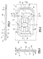
- FIG. 1 shows a standardized card C, of known general design, which is a smart card essentially consisting of a 10. plate-shaped body rectangular with rounded corners which is generally made of plastic and which incorporates an electronic microcircuit (not shown) which is associated with the support 10 according to one any of the known techniques, for example under the form of a module inserted in the support 10.
- the face 12 of the card C visible in FIG. 1 is the front of the card which has an area 14 in which are arranged six tracks 16, or pads, of electrical connection from the electronic microcircuit to an operating circuit by via an electrical connector (not shown) belonging for example to a read-write device.
- the pads 16 are arranged according to a design standardized and they extend globally parallel the to each other and aligned two by two according to the direction general longitudinal of the map, i.e. according to the direction parallel to the two parallel longitudinal edges and opposites 18 and 20 of the support 10.
- zone 14 comprising the series of tracks 16 is arranged near an edge transverse 22 of the support 10 which is called here transverse edge before with reference to the usual direction of introduction of the card C, from back to front, in a connector.
- the support 10 is also delimited by a transverse edge opposite rear 24 parallel to the front transverse edge 22 and perpendicular to the two longitudinal edges 18 and 20.
- the other side 13 forming the back of the card (see Figure 3) is parallel to the front face 12, these two faces determining the standardized thickness of the card C which is between 0.68 and 0.84 mm and preferably between 0.80 and 0.84 mm.
- the support 10 comprises a slot F of substantially rectangular outline and which generally extends around a portion of the body 10 of the card C which includes the electronic microcircuit and zone 14 comprising the series of electrical connection pads 16.
- Slot F thus internally delimits a mini-card standardized MC, of substantially rectangular outline, which is delimited by two parallel and opposite longitudinal edges 26 and 28 which are respectively parallel and adjacent to longitudinal edges 18 and 20 of card C.
- the minimap MC is also delimited by a first edge transverse 30, here called front transverse edge, which is parallel and adjacent to the front transverse edge 22 of the card vs.
- the MC minimap is also delimited by another rear transverse edge 32 opposite and parallel to the edge transverse before 30, which is an edge having a chamfer 34 formed in the front 12 of the support 10 and which is connected to the longitudinal edge 28 by a cutaway 36, of shape and standard dimensions, to provide a means of coding of the direction of introduction or placement of the MC mini-card in a connector.
- the chamfer has the function of avoiding a possible hooking of the minimap against the organs of a mobile by telephone, when it is removed from it. Indeed, some mobiles have elastic means which tend to press the minimap against the connector and lift the end 32 of the minimap outside the general map plane.
- the chamfer can be achieved by compression of the material of the card using appropriate tools.
- Slot F can be produced using a technique known, for example by using a cut / punch and a complementary die, or by making it by cutting by means of a pressurized water jet or a laser beam.
- the connecting straps are made from matter, i.e. they are made up of portions of the support 10 which are not cut during the production from slot F.
- the three connecting straps are distributed according to an arrangement which will now be described in more detail, in particular with reference to FIG. 2.
- the first strap B1 extends longitudinally, towards the left considering figure 2, from the edge transverse before 30 of the minimap MC which is adjacent to the zone 14 and this in the direction of the front transverse edge 22 of the card C.
- the first strap B1 is a wide strap L1, for example equal to about 11 mm, which is greater than the width L2 representative of the width and passage of the blades of contact of a connector with respect to zone 14 carrying the electrical connection pads 16.
- the B1 strap extends at least opposite this area so that there have no slit portion F between the front transverse edge 22 of card C and zone 14 to avoid damaging the contacts of a connector through the passage of a slot portion F on the free ends of the connector contact.
- the first wide B1 strap L1 imparts mechanical properties to the C card and the minimap MC allowing them to resist in association with the other straps to torsional and bending forces previously mentioned.
- the two other connecting straps of the MC mini-card à la carte C are, in the embodiment illustrated in the figures, two identical and opposite suspenders B2 and B3.
- the first strap B2 extends transversely to from the longitudinal edge 26 of the minimap MC towards from the longitudinal edge 18 of the card C.
- the third B3 ramp extends transversely from the longitudinal edge 28 of the MC mini-map towards the longitudinal edge 20 of the map vs.
- the second and third straps B2 and B3 are aligned in the same transverse direction and they are located near zone 14, i.e. their axis transverse mean, corresponding to the line 4-4 of the Figure 2, is located at a distance from the front transverse edge 30 of the minimap MC substantially equal to 17 mm.
- the second and third suspenders B2 and B3 are suspenders of reduced width L3 which is for example equal to approximately 1.2 mm.
- the three straps B1 to B3 are suspenders each delimited by two edges parallel and opposite, of longitudinal orientation in the case of the first ramp B1, and of transverse orientation in the case of the second and third suspenders B2 and B3.
- the means constituting links of rupture of the connecting straps are grooves of particular profiles and dimensions.
- front 12 and the back 13 of the strap each have a groove 40, 42 which are opposite and aligned and each of which is conformed in section, as can be seen in particular in Figures 3 and 5, with a substantially V-shaped profile.
- each groove 40, 42 comprises a vertical branch or edge 44, 46 which extends vertically perpendicular to the plane of front 12, back 13 while the other edges or branches 48 and 49 are inclined in the direction of card C, at an acute angle with edge 44, 46 by example equal to around 30 °.
- the depths of the grooves 40 and 42 are preferably equal but they can be different and for example equal to 0.42 and 0.30 mm in the case of a 0.82 mm thick card.
- the tip of the groove is broken by a flat width equal to approximately 0.02 mm or substantially equivalent by a rounding of radius of curvature equal to approximately 0.01 mm.
- the residual section between the grooves depends on the thickness of the card and the nature of the constituent material of support. The above values are given for a card in injected ABS or ABS - HR (high temperature) and correspond to a residual section equal to approximately 0.10 mm. These values would however be appreciably valid for cards obtained from another injected material and similar mechanical properties.
- the grooves are made by marking by means a punch (not shown in the figures) including La depth of penetration determines the depth of grooves.
- the grooves forming a starting point 40 and 42 extend over the entire width L1 of the strap B1.
- the grooves 50 formed on the front 12 of the straps B2 and B3 are not identical to the grooves 52 formed in the back 13. They on the other hand are identical two by two, that is to say that the two grooves 50 formed in the front 12 are identical, of same as the two grooves 52 formed in the back 13.
- the width of the grooves 50 is less than the total width L3 of the first and second suspenders B2 and B3. The same is true of the width of the grooves 52.
- the grooves 52 forming a starting point which are formed in verso 13 are similar in design to that grooves 40 and 42 formed in the first strap B1, that is to say that each has a profile substantially in V shape with an edge 54 perpendicular to the general plane of card C and an inclined edge 56.
- the angle of V is here by example of 25 ° and the depth of the grooves 52 is 0.10mm.
- the grooves preferably have an angle rounded at their end (at the tip of the V). Thanks to this rounding, the triggering and propagation of cracks is limited to course of bending torsion tests according to ISO standard supra. This rounding presents in the example in particular a radius of curvature of the order of 0.01 mm.
- the groove is sufficiently profiled so as to allow initiation of rupture by pressure manual manual acting on the minimap by going especially from front to back
- the grooves 50 have a different profile substantially trapezoid-shaped illustrated in particular in figure 7.
- each groove 50 is delimited by a bottom 58 slightly inclined compared to front 12 and to the general plan of card C, for example at an angle of 10 °, which corresponds to the small base 58 of the trapezoid, the latter being moreover delimited by a large side 60, aligned with the edge 54 of the opposite groove 52, which extends perpendicular to the plan of recto 12 and the general plan of the large map and, on the other hand, by a small side 62 which is inclined, the first side 60 being adjacent to the MC minimap while the side inclined (or rather slightly rounded) 62 extends in the direction from the body of the card C.
- the sides 60 and 62 are connected to the bottom 58 with leaves of about 0.05 mm radius.
- the grooves 52 and 50 have a width L4 which is for example equal to 0.40 mm while the width L3 of the straps B2 and B3 is equal to approximately 1, 2 mm.
- the width of the groove 50 is equal to about 0.22 mm.
- This groove is shaped so as to resist bending / torsion forces imposed on the aforementioned ISO standard and this more significantly than the groove 52. Indeed, its rounded and open shape is more resistant to triggering of a crack than that of groove 52 which has an acute shape and ends with a small radius of equal curvature for example 0.01 mm, as opposed to groove 50, the deepest end of which example a radius of curvature greater than 0.05 mm.
- a slight inclination of the bottom 58 of the groove 50 creates an area closest to the end of the groove 52. This gives a zone 69 initiation or arrival of a crack, facilitating the breaking of the strap along a line joining edges 60 and 54.
- groove 50 is more flared than the groove 52, this always for the purpose to be less sensitive to a crack initiation compared to groove 52
- the card has shoulder straps connecting the minimap to the large card of particular shape, each strap including two types of grooves facing each other shaped so as to be sufficiently resistant to the efforts of bending / twisting according to ISO standard, one of the grooves being however also more easily conformed to initiate a crack by voluntary manual pressure on the minimap.
- each strap including two types of grooves facing each other shaped so as to be sufficiently resistant to the efforts of bending / twisting according to ISO standard, one of the grooves being however also more easily conformed to initiate a crack by voluntary manual pressure on the minimap.
- the strap B1 is produced in two straps B4, B5 spaced apart, particularly near the corners. 70, 71 of the minimap. These suspenders may have grooves whose section is substantially in line with that of shoulder strap B1 (figure. 5).
- the advantage of a two-strap construction is allow the minimap to be kept substantially in a plane despite a curvature of the card across its width. We avoid thus a likely tendency of the B1 ramp to have a crack initiation from angles 70, 71.
- suspenders B4, B5 conforms to straps B2, B3 to increase resistance to bending / twisting forces.
- this central strap can be conforms to B4, B5 is dimensioned to fill the expected function .
- the additional function of the B1 strap which is to facilitate the passage of elastic connector blades can be done in two other different ways.
- the first is illustrated in Figures 9 and 10, by chamfers which reduce the discontinuity caused by the slot F.
- the chamfers are provided at the level of the passage of these elastic blades in the event of significant discontinuity.
- a chamfer 72, 73 is provided respectively each side of slot F.
- the slot F can be made in accordance with the notch 74 of FIG. 12 over the entire contour of the minimap with the exception of the suspenders.
Description
- la figure 1 est une vue en plan de dessus d'une carte conforme aux enseignements de l'invention ;
- la figure 2 est une vue similaire à celle de la figure 1 sur laquelle on a représenté à plus grande échelle la partie de la carte comportant la minicarte ;
- les figures 3 et 4 sont des vues en section selon les lignes 3-3 et 4-4 de la figure 2 ;
- la figure 5 est une vue à plus grande échelle du détail D5 de la figure 3 ;
- la figuré 6 est une vue partielle en section selon la ligne 6-6 de la figure 5 ;
- la figure 7 est une vue à plus grande échelle du détail D7 de la figure 4 ; et
- la figure 8 est une vue partielle en section selon la ligne 8-8 de la figure 7.
- la figure 9 est une vue en plan de dessus d'une autre carte conforme aux enseignements de l'invention;
- la figure 10 est une vue partielle en section selon la ligne 10-10 de la figure 9;
- la figure. 11 est une vue en plan de dessus d'une autre carte conforme aux enseignements de l'invention;
- la figure 12 est une vue partielle en section selon la ligne12-12 de la figure 11;
Claims (12)
- Carte normalisée (C) à circuit(s) intégré(s) à contact comportant un support (10) délimité par deux grands bords longitudinaux (18, 20) et par deux petits bords transversaux avant (22) et arrière (24), qui porte au moins un microcircuit électronique et dont le recto (12) comporte une série (14) de plages de contact (16), agencée au voisinage du bord transversal avant (22) de la carte (C), et comportant une fente (F) de contour sensiblement rectangulaire formée dans le support (10), autour d'une portion comportant le microcircuit et la sérié (14) de plages de contact (16), pour délimiter une minicarte (MC) normalisée détachable qui est reliée au support (10) de la carte (C) par une ou plusieurs bretelles (B1, B2, B3), qui s'étendent entre les bords intérieurs de la découpe et les bords en vis-à-vis (26, 28, 30, 32),
caractérisée en ce qu'au moins une bretelle comporte deux types de rainures (50, 52) en regard l'une de l'autre, l'une (50) étant conformée de manière à résister au déclenchement de fissures au cours d'efforts de flexion/torsion selon la norme ISO et ce de manière plus importante que l'autre rainure (52), cette dernière étant cependant également conformée de manière à amorcer une fissure par pression manuelle volontaire sur la minicarte. - Carte selon la revendication 1, caractérisée en ce qu'elle comporte trois bretelles (B1, B2, B3) de liaison parmi lesquelles une première bretelle (B1) qui s'étend longitudinalement depuis le bord transversal avant (30) de la minicarte (MC) adjacent au bord transversal avant (22) de la carte (C), dont la largeur (L1) est au moins égale à la largeur (L2) de la série (14) des plages de contact (16) agencée au voisinage du bord transversal avant (30) de la minicarte (MC), et des deuxième (B2) et troisième (B3) bretelles opposées qui s'étendent chacune transversalement à partir d'un bord longitudinal (26, 28) de la minicarte (MC).
- Carte selon l'une des revendications précédentes, caractérisée en ce que les deuxième (B2) et troisième (B3) bretelles sont alignées transversalement et sont situées à proximité de la série (14) des plages de contact (16).
- Carte selon l'une des revendications précédentes, caractérisée en ce que les deuxième (B2) et troisième (B3) bretelles alignées sont situées à environ 17 mm dudit bord transversal avant (30) de la minicarte (MC) à partir duquel s'étend la première bretelle (B1).
- Carte selon l'une quelconque des revendications précédentes, caractérisée en ce que la largeur (L1) de la première (B1) bretelle est égale à environ 11 mm.
- Carte selon l'une quelconque des revendications précédentes, caractérisée en ce que la largeur (L3) des deuxième (B2) et troisième (B3) bretelles est égale à environ 1, 2 mm.
- Carte selon l'une quelconque des revendications précédentes, caractérisée en ce que chacune des bretelles (B1, B2, B3) comporte, au moins sur son recto (12) ou son verso (13), une rainure (40, 42, 50, 52) parallèle au bord de la minicarte (MC) à partir duquel la bretelle s'étend de manière à constituer une portion d'épaisseur réduite constituant une amorce de rupture de la bretelle.
- Carte selon la revendication précédente, caractérisée en ce que la première bretelle (B1) comporte, au moins sur son recto (12) ou son verso (13), une rainure (40, 42) qui, en section, présente un profil en V dont une branche (44, 46) adjacente au bord (30) de la minicarte (MC) s'étend perpendiculairement au plan général de la carte (C).
- Carte selon la revendication précédente, caractérisée en ce que la première bretelle (B1) comporte deux rainures (40, 42) opposées identiques et alignées formées dans le recto (12) et le verso (13).
- Carte selon l'une quelconque des revendications 7 à 9, caractérisée en ce que chacune des deuxième, (B2) et troisième (B3) bretelles comporte, au moins sur son recto ou son verso, une rainure (52) qui, en section, présente un profil en V dont une branche (54) adjacente au bord (28, 26) de la minicarte (MC) s'étend perpendiculairement au plan général de la carte (C).
- Carte selon l'une quelconque des revendications 7 à 9, caractérisée en ce que chacune des deuxième (B2) et troisième (B3) bretelles comporte, au moins sur son recto ou son verso, une rainure (50) qui, en section, présente un profil sensiblement en forme de trapèze dont un côté (60) adjacent au bord (28, 26) de la minicarte (MC) s'étend perpendiculairement au plan général de la carte (C) et dont la petite base (58) appartenant au fond de la rainure s'étend avec une inclinaison par rapport au plan général de la carte (C).
- Carte selon la revendication 11 prise en combinaison avec la revendication 10, caractérisée en ce que chacune des deuxième (B2) et troisième (B3) bretelles comporte deux rainures opposées et alignées, sur son verso (13) une rainure (52) en forme de V et sur son recto (12) une rainure (50) en forme de trapèze.
Applications Claiming Priority (3)
| Application Number | Priority Date | Filing Date | Title |
|---|---|---|---|
| FR9801370A FR2773900B1 (fr) | 1998-01-22 | 1998-01-22 | Carte a circuit(s) integre(s) a contact, comportant une minicarte detachable |
| FR9801370 | 1998-01-22 | ||
| PCT/FR1999/000052 WO1999038118A2 (fr) | 1998-01-22 | 1999-01-14 | Carte a circuit(s) integre(s) a contact, comportant une minicarte detachable |
Publications (2)
| Publication Number | Publication Date |
|---|---|
| EP1050018A2 EP1050018A2 (fr) | 2000-11-08 |
| EP1050018B1 true EP1050018B1 (fr) | 2002-10-16 |
Family
ID=9522647
Family Applications (1)
| Application Number | Title | Priority Date | Filing Date |
|---|---|---|---|
| EP99900916A Expired - Lifetime EP1050018B1 (fr) | 1998-01-22 | 1999-01-14 | Carte a circuit(s) integre(s) a contact, comportant une minicarte detachable |
Country Status (11)
| Country | Link |
|---|---|
| US (1) | US6448638B1 (fr) |
| EP (1) | EP1050018B1 (fr) |
| JP (1) | JP2002501264A (fr) |
| CN (1) | CN1294718A (fr) |
| AT (1) | ATE226343T1 (fr) |
| AU (1) | AU2057899A (fr) |
| CA (1) | CA2318967A1 (fr) |
| DE (1) | DE69903513T2 (fr) |
| ES (1) | ES2186319T3 (fr) |
| FR (1) | FR2773900B1 (fr) |
| WO (1) | WO1999038118A2 (fr) |
Families Citing this family (44)
| Publication number | Priority date | Publication date | Assignee | Title |
|---|---|---|---|---|
| FR2783948B1 (fr) * | 1998-09-24 | 2000-11-10 | Gemplus Card Int | Carte a puce grand format comprenant une mini-carte detachable et procede de fabrication |
| FR2794264B1 (fr) * | 1999-05-27 | 2001-11-02 | Gemplus Card Int | Adaptateur pour dispositif electronique portable a circuit integre, de type carte a puce, d'un format reduit par rapport au format standard d'une mini-carte |
| US7487908B1 (en) * | 1999-10-23 | 2009-02-10 | Ultracard, Inc. | Article having an embedded accessible storage member, apparatus and method for using same |
| FR2806661B1 (fr) * | 2000-03-21 | 2002-11-08 | Sagem | Carte a puce pouvant subir des contraintes de flexion |
| WO2001084490A1 (fr) * | 2000-04-28 | 2001-11-08 | Hitachi,Ltd | Carte a circuit integre |
| JP2002170095A (ja) * | 2000-12-01 | 2002-06-14 | Dainippon Printing Co Ltd | 板状枠体付きicキャリア |
| FR2819081B1 (fr) * | 2000-12-28 | 2004-12-03 | Gemplus Card Int | Carte a puce a structure composee et procede de fabrication |
| JP2002236895A (ja) * | 2001-02-07 | 2002-08-23 | Dainippon Printing Co Ltd | 板状枠体付きicキャリア |
| JP4770031B2 (ja) * | 2001-02-08 | 2011-09-07 | 大日本印刷株式会社 | 板状枠体付きicキャリアとその製造方法 |
| FR2829267B1 (fr) * | 2001-09-05 | 2003-12-12 | Gemplus Card Int | Carte du type carte a puce comprenant un support plan sensiblement rectangulaire |
| FR2833736B1 (fr) * | 2001-12-18 | 2004-05-14 | Gemplus Card Int | Carte du type carte a puce |
| FR2834103B1 (fr) * | 2001-12-20 | 2004-04-02 | Gemplus Card Int | Carte a puce a module de surface etendue |
| US6899276B2 (en) * | 2002-02-15 | 2005-05-31 | Axalto Sa | Wrapped-card assembly and method of manufacturing the same |
| EP1380990A1 (fr) * | 2002-07-09 | 2004-01-14 | SCHLUMBERGER Systèmes | Support de données inséré dans un autre support de données d'un type différent |
| EP1413978A1 (fr) * | 2002-10-24 | 2004-04-28 | SCHLUMBERGER Systèmes | Support de données |
| WO2005081181A1 (fr) * | 2004-02-20 | 2005-09-01 | Renesas Technology Corp. | Procede de fabrication d’une carte imprimee et carte imprimee |
| US6939182B1 (en) * | 2004-04-20 | 2005-09-06 | C-One Technology Corporation | Fool-proof mechanism for memory card |
| FR2872946B1 (fr) * | 2004-07-08 | 2006-09-22 | Gemplus Sa | Procede de fabrication d'un support de carte a puce mini uicc avec adaptateur plug-in uicc associe et support obtenu |
| EP1727080A1 (fr) * | 2005-05-27 | 2006-11-29 | Axalto S.A. | SIM ayant deux jeux de contacts protégés contre un court-circuit |
| US20070012788A1 (en) * | 2005-07-15 | 2007-01-18 | Chien-yuan Chen | Manufacturing process for encapsulation and cutting memory cards |
| DE102005059964A1 (de) * | 2005-12-15 | 2007-06-28 | Giesecke & Devrient Gmbh | Verfahren zum Herstellen eines kartenförmigen Datenträgers |
| FR2951867A1 (fr) * | 2009-10-27 | 2011-04-29 | Arjowiggins Security | Procede de fabrication d'un support comportant un dispositif electronique |
| CH703738B1 (de) | 2010-08-31 | 2018-05-31 | Swisscom Ag | SIM-Karte und Verfahren zur Herstellung derselben. |
| FR2974925B1 (fr) | 2011-05-02 | 2013-06-14 | Oberthur Technologies | Procede de preparation d'un support de carte a base de cellulose pour minicarte |
| EP2568418B1 (fr) * | 2011-09-12 | 2015-08-19 | Oberthur Technologies | Carte de microcircuit et outil et procédé pour marquer une telle carte |
| US8649820B2 (en) | 2011-11-07 | 2014-02-11 | Blackberry Limited | Universal integrated circuit card apparatus and related methods |
| US8950681B2 (en) | 2011-11-07 | 2015-02-10 | Blackberry Limited | Universal integrated circuit card apparatus and related methods |
| USD691610S1 (en) | 2011-11-07 | 2013-10-15 | Blackberry Limited | Device smart card |
| USD702693S1 (en) * | 2011-11-23 | 2014-04-15 | Digital Hard Copy | Digital storage medium card |
| USD702692S1 (en) * | 2011-11-23 | 2014-04-15 | Digital Hard Copy | Card for holding a digital storage medium |
| FR2983325B1 (fr) * | 2011-11-24 | 2014-06-20 | Oberthur Technologies | Procede de decoupage d'une couche a inclure dans une carte support de donnees et carte support de donnees produite en utilisant un tel procede |
| ITMI20112415A1 (it) * | 2011-12-28 | 2013-06-29 | St Microelectronics Srl | Modulo sim |
| DE102012001776A1 (de) * | 2012-01-31 | 2013-08-01 | Giesecke & Devrient Gmbh | Chipkarte mit heraustrennbarer Miniaturchipkarte |
| USD703208S1 (en) * | 2012-04-13 | 2014-04-22 | Blackberry Limited | UICC apparatus |
| US8936199B2 (en) | 2012-04-13 | 2015-01-20 | Blackberry Limited | UICC apparatus and related methods |
| USD701864S1 (en) * | 2012-04-23 | 2014-04-01 | Blackberry Limited | UICC apparatus |
| CN102831733B (zh) * | 2012-08-13 | 2015-06-10 | 深圳市新国都技术股份有限公司 | 分体式银行卡结构及通过智能终端实现无线支付的方法 |
| USD707682S1 (en) * | 2012-12-05 | 2014-06-24 | Logomotion, S.R.O. | Memory card |
| FR3007682B1 (fr) | 2013-07-01 | 2016-01-08 | Oberthur Technologies | Outillage et procede de fragilisation d'un contour dans une carte plastique mince |
| JP2015060392A (ja) | 2013-09-18 | 2015-03-30 | 株式会社東芝 | Icカード用基材、icカードの製造方法、及びicカード |
| FR3015087B1 (fr) | 2013-12-13 | 2017-05-12 | Plastifrance | Support de cartes de formats multiples et a positionnement reversible stable. |
| ES2542651B1 (es) * | 2014-02-07 | 2016-07-19 | Valid Soluciones Tecnologicas, S.A.U. | Soporte de tarjeta con mini tarjeta inteligente extraíble y procedimiento de fabricación del mismo. |
| US9147147B2 (en) * | 2014-02-26 | 2015-09-29 | Giesecke & Devrient America, Inc. | Plug-in portable data carrier with semi-detachable token holder |
| JP2016015084A (ja) * | 2014-07-03 | 2016-01-28 | 株式会社東芝 | Icカード |
Family Cites Families (18)
| Publication number | Priority date | Publication date | Assignee | Title |
|---|---|---|---|---|
| JPS5968072A (ja) * | 1982-10-13 | 1984-04-17 | Sharp Corp | 機能変換用小形電子機器 |
| FR2590051B1 (fr) * | 1985-11-08 | 1991-05-17 | Eurotechnique Sa | Carte comportant un composant et micromodule a contacts de flanc |
| JPH01192590A (ja) * | 1988-01-28 | 1989-08-02 | Asahi Chem Ind Co Ltd | 携帯可能電子装置 |
| JPH02292692A (ja) * | 1989-05-08 | 1990-12-04 | Hitachi Ltd | カードデータ処理方法 |
| JPH0355296A (ja) * | 1989-07-25 | 1991-03-11 | Toshiba Corp | Icカード及びそのicカードに用いられるicモジュール並びにカード本体 |
| FR2678753B1 (fr) * | 1991-07-02 | 1996-12-20 | Gemplus Card Int | Fabrication de cartes a puce a module autodetachable. |
| JPH05229292A (ja) * | 1992-02-25 | 1993-09-07 | Toppan Printing Co Ltd | Icカード |
| JPH05238182A (ja) * | 1992-02-28 | 1993-09-17 | Citizen Watch Co Ltd | Icカードの構造 |
| US5581065A (en) * | 1993-08-02 | 1996-12-03 | Dai Nippon Printing Co., Ltd. | Sheet-framed IC carrier, method for producing the same, and IC carrier case |
| JPH0822523A (ja) * | 1994-07-07 | 1996-01-23 | Mitsubishi Plastics Ind Ltd | Icメモリカード |
| JPH08123917A (ja) * | 1994-09-02 | 1996-05-17 | Mitsubishi Electric Corp | Icカード及びicカードシステム |
| US5956601A (en) * | 1996-04-25 | 1999-09-21 | Kabushiki Kaisha Toshiba | Method of mounting a plurality of semiconductor devices in corresponding supporters |
| US5752857A (en) * | 1996-05-24 | 1998-05-19 | Itt Corporation | Smart card computer adaptor |
| JPH09327990A (ja) * | 1996-06-11 | 1997-12-22 | Toshiba Corp | カード型記憶装置 |
| JPH11134466A (ja) * | 1997-10-29 | 1999-05-21 | Kyodo Printing Co Ltd | Icカード |
| JP2000305662A (ja) * | 1999-04-23 | 2000-11-02 | Jst Mfg Co Ltd | カード接続用アダプタ |
| FR2794059B1 (fr) * | 1999-05-31 | 2001-08-10 | Gemplus Card Int | Dispositif portable a circuit integre et procede de fabrication |
| DE20008692U1 (de) * | 2000-05-15 | 2000-08-31 | Scm Microsystems Gmbh | Schnittstellenvorrichtung für Chipkarten |
-
1998
- 1998-01-22 FR FR9801370A patent/FR2773900B1/fr not_active Expired - Fee Related
-
1999
- 1999-01-14 JP JP2000528950A patent/JP2002501264A/ja active Pending
- 1999-01-14 AU AU20578/99A patent/AU2057899A/en not_active Abandoned
- 1999-01-14 CN CN99804359A patent/CN1294718A/zh active Pending
- 1999-01-14 CA CA002318967A patent/CA2318967A1/fr not_active Abandoned
- 1999-01-14 AT AT99900916T patent/ATE226343T1/de not_active IP Right Cessation
- 1999-01-14 WO PCT/FR1999/000052 patent/WO1999038118A2/fr active IP Right Grant
- 1999-01-14 EP EP99900916A patent/EP1050018B1/fr not_active Expired - Lifetime
- 1999-01-14 ES ES99900916T patent/ES2186319T3/es not_active Expired - Lifetime
- 1999-01-14 US US09/600,706 patent/US6448638B1/en not_active Expired - Lifetime
- 1999-01-14 DE DE69903513T patent/DE69903513T2/de not_active Expired - Lifetime
Also Published As
| Publication number | Publication date |
|---|---|
| EP1050018A2 (fr) | 2000-11-08 |
| AU2057899A (en) | 1999-08-09 |
| ES2186319T3 (es) | 2003-05-01 |
| WO1999038118A2 (fr) | 1999-07-29 |
| DE69903513T2 (de) | 2003-06-26 |
| WO1999038118A3 (fr) | 1999-11-04 |
| CN1294718A (zh) | 2001-05-09 |
| ATE226343T1 (de) | 2002-11-15 |
| JP2002501264A (ja) | 2002-01-15 |
| FR2773900B1 (fr) | 2000-02-18 |
| FR2773900A1 (fr) | 1999-07-23 |
| DE69903513D1 (de) | 2002-11-21 |
| US6448638B1 (en) | 2002-09-10 |
| CA2318967A1 (fr) | 1999-07-29 |
Similar Documents
| Publication | Publication Date | Title |
|---|---|---|
| EP1050018B1 (fr) | Carte a circuit(s) integre(s) a contact, comportant une minicarte detachable | |
| EP0803835B2 (fr) | Connecteur électrique de faible encombrement pour une carte à mémoire électronique | |
| FR2821988A1 (fr) | Connecteur electrique pour cartes a memoire electronique a grande capacite de stockage | |
| CA2429435C (fr) | Carte a puce sans contact ou hybride contact-sans contact a tenue renforcee du module electronique | |
| FR2794264A1 (fr) | Adaptateur pour dispositif electronique portable a circuit integre, de type carte a puce, d'un format reduit par rapport au format standard d'une mini-carte | |
| EP1927941A1 (fr) | Carte à puce comportant une antenne et procédé de fabrication | |
| WO2000017814A1 (fr) | Carte a puce grand format comprenant une mini-carte detachable et procede de fabrication | |
| EP1433127B1 (fr) | Carte du type carte a puce comprenant un support plan sensiblement rectangulaire | |
| FR2660092A1 (fr) | Procede de fabrication d'une carte a circuit integre. | |
| EP0766875B1 (fr) | Connecteur electrique, notamment pour le raccordement d'une carte a memoire electronique | |
| EP1080446B1 (fr) | Carte a circuit integre du type bi-standard comportant une fente d'isolement | |
| EP0738983B1 (fr) | Connecteur électrique pour une carte à circuit(s) intégré(s) à contact | |
| FR2828953A1 (fr) | Procede de fabrication d'une carte munie d'un organe de commande et carte de ce type | |
| WO1995033243A1 (fr) | Connecteur electrique pour le raccordement d'une carte a memoire electronique comportant un commutateur integre de detection de la presence d'une carte | |
| EP0720761B1 (fr) | Etui recepteur pour une carte a circuit(s) integre(s) a contact | |
| EP1405260B2 (fr) | Carte a microcircuit avec plaquette detachable | |
| EP1546989B1 (fr) | Lecteur de carte a puce a boitier transparent | |
| FR2843655A1 (fr) | Broche a emmanchement a force | |
| EP1552541B1 (fr) | Clavier etanche | |
| FR3079645A1 (fr) | Document electronique dont une liaison electrique entre un port de puce et une plage externe de contact electrique est etablie via un inlay | |
| WO1999054846A1 (fr) | Procede de fabrication d'une carte a circuit integre a contact et une carte obtenue selon ce procede | |
| FR3131035A1 (fr) | Support de carte SIM et éjecteur de carte SIM | |
| WO1998041946A1 (fr) | Connecteur pour lecteur de carte, a contacts balais elastiques, et lecteur comportant un tel connecteur | |
| FR2658364A1 (fr) | Connecteur electrique pour cartes a memoire electronique. | |
| EP3136303B1 (fr) | Carte et procédé de fabrication correspondant |
Legal Events
| Date | Code | Title | Description |
|---|---|---|---|
| PUAI | Public reference made under article 153(3) epc to a published international application that has entered the european phase |
Free format text: ORIGINAL CODE: 0009012 |
|
| 17P | Request for examination filed |
Effective date: 20000822 |
|
| AK | Designated contracting states |
Kind code of ref document: A2 Designated state(s): AT BE CH DE DK ES FR GB IT LI PT |
|
| 17Q | First examination report despatched |
Effective date: 20010216 |
|
| GRAG | Despatch of communication of intention to grant |
Free format text: ORIGINAL CODE: EPIDOS AGRA |
|
| GRAG | Despatch of communication of intention to grant |
Free format text: ORIGINAL CODE: EPIDOS AGRA |
|
| GRAH | Despatch of communication of intention to grant a patent |
Free format text: ORIGINAL CODE: EPIDOS IGRA |
|
| GRAH | Despatch of communication of intention to grant a patent |
Free format text: ORIGINAL CODE: EPIDOS IGRA |
|
| GRAA | (expected) grant |
Free format text: ORIGINAL CODE: 0009210 |
|
| AK | Designated contracting states |
Kind code of ref document: B1 Designated state(s): AT BE CH DE DK ES FR GB IT LI PT |
|
| PG25 | Lapsed in a contracting state [announced via postgrant information from national office to epo] |
Ref country code: AT Free format text: LAPSE BECAUSE OF FAILURE TO SUBMIT A TRANSLATION OF THE DESCRIPTION OR TO PAY THE FEE WITHIN THE PRESCRIBED TIME-LIMIT Effective date: 20021016 |
|
| REF | Corresponds to: |
Ref document number: 226343 Country of ref document: AT Date of ref document: 20021115 Kind code of ref document: T |
|
| REG | Reference to a national code |
Ref country code: GB Ref legal event code: FG4D Free format text: NOT ENGLISH |
|
| REG | Reference to a national code |
Ref country code: CH Ref legal event code: EP |
|
| REF | Corresponds to: |
Ref document number: 69903513 Country of ref document: DE Date of ref document: 20021121 |
|
| PG25 | Lapsed in a contracting state [announced via postgrant information from national office to epo] |
Ref country code: PT Free format text: LAPSE BECAUSE OF FAILURE TO SUBMIT A TRANSLATION OF THE DESCRIPTION OR TO PAY THE FEE WITHIN THE PRESCRIBED TIME-LIMIT Effective date: 20030116 Ref country code: DK Free format text: LAPSE BECAUSE OF FAILURE TO SUBMIT A TRANSLATION OF THE DESCRIPTION OR TO PAY THE FEE WITHIN THE PRESCRIBED TIME-LIMIT Effective date: 20030116 |
|
| PG25 | Lapsed in a contracting state [announced via postgrant information from national office to epo] |
Ref country code: LI Free format text: LAPSE BECAUSE OF NON-PAYMENT OF DUE FEES Effective date: 20030131 Ref country code: CH Free format text: LAPSE BECAUSE OF NON-PAYMENT OF DUE FEES Effective date: 20030131 Ref country code: BE Free format text: LAPSE BECAUSE OF NON-PAYMENT OF DUE FEES Effective date: 20030131 |
|
| GBT | Gb: translation of ep patent filed (gb section 77(6)(a)/1977) |
Effective date: 20030129 |
|
| REG | Reference to a national code |
Ref country code: ES Ref legal event code: FG2A Ref document number: 2186319 Country of ref document: ES Kind code of ref document: T3 |
|
| PLBI | Opposition filed |
Free format text: ORIGINAL CODE: 0009260 |
|
| PLAX | Notice of opposition and request to file observation + time limit sent |
Free format text: ORIGINAL CODE: EPIDOSNOBS2 |
|
| 26 | Opposition filed |
Opponent name: GIESECKE & DEVRIENT GMBH Effective date: 20030716 |
|
| REG | Reference to a national code |
Ref country code: CH Ref legal event code: PL |
|
| PLAX | Notice of opposition and request to file observation + time limit sent |
Free format text: ORIGINAL CODE: EPIDOSNOBS2 |
|
| PLBB | Reply of patent proprietor to notice(s) of opposition received |
Free format text: ORIGINAL CODE: EPIDOSNOBS3 |
|
| PLBP | Opposition withdrawn |
Free format text: ORIGINAL CODE: 0009264 |
|
| PLBD | Termination of opposition procedure: decision despatched |
Free format text: ORIGINAL CODE: EPIDOSNOPC1 |
|
| PLBD | Termination of opposition procedure: decision despatched |
Free format text: ORIGINAL CODE: EPIDOSNOPC1 |
|
| PLBM | Termination of opposition procedure: date of legal effect published |
Free format text: ORIGINAL CODE: 0009276 |
|
| STAA | Information on the status of an ep patent application or granted ep patent |
Free format text: STATUS: OPPOSITION PROCEDURE CLOSED |
|
| 27C | Opposition proceedings terminated |
Effective date: 20050508 |
|
| REG | Reference to a national code |
Ref country code: FR Ref legal event code: TP Ref country code: FR Ref legal event code: CD |
|
| REG | Reference to a national code |
Ref country code: GB Ref legal event code: S117 Free format text: REQUEST FILED; REQUEST FOR CORRECTION UNDER SECTION 117 FILED ON 26 APRIL 2010 |
|
| REG | Reference to a national code |
Ref country code: GB Ref legal event code: 732E Free format text: REGISTERED BETWEEN 20110616 AND 20110622 |
|
| REG | Reference to a national code |
Ref country code: DE Ref legal event code: R082 Ref document number: 69903513 Country of ref document: DE Representative=s name: HOFFMANN - EITLE, DE |
|
| REG | Reference to a national code |
Ref country code: DE Ref legal event code: R082 Ref document number: 69903513 Country of ref document: DE Representative=s name: HOFFMANN - EITLE, DE Effective date: 20120629 Ref country code: DE Ref legal event code: R082 Ref document number: 69903513 Country of ref document: DE Representative=s name: HOFFMANN - EITLE PATENT- UND RECHTSANWAELTE PA, DE Effective date: 20120629 Ref country code: DE Ref legal event code: R081 Ref document number: 69903513 Country of ref document: DE Owner name: GEMALTO SA, FR Free format text: FORMER OWNER: GEMPLUS, GEMENOS, FR Effective date: 20120629 |
|
| REG | Reference to a national code |
Ref country code: ES Ref legal event code: PC2A Owner name: GEMALTO S.A. Effective date: 20131205 |
|
| REG | Reference to a national code |
Ref country code: FR Ref legal event code: PLFP Year of fee payment: 18 |
|
| REG | Reference to a national code |
Ref country code: FR Ref legal event code: PLFP Year of fee payment: 19 |
|
| REG | Reference to a national code |
Ref country code: FR Ref legal event code: PLFP Year of fee payment: 20 |
|
| PGFP | Annual fee paid to national office [announced via postgrant information from national office to epo] |
Ref country code: FR Payment date: 20171221 Year of fee payment: 20 |
|
| PGFP | Annual fee paid to national office [announced via postgrant information from national office to epo] |
Ref country code: GB Payment date: 20171222 Year of fee payment: 20 |
|
| PGFP | Annual fee paid to national office [announced via postgrant information from national office to epo] |
Ref country code: ES Payment date: 20180201 Year of fee payment: 20 Ref country code: DE Payment date: 20171218 Year of fee payment: 20 |
|
| PGFP | Annual fee paid to national office [announced via postgrant information from national office to epo] |
Ref country code: IT Payment date: 20180102 Year of fee payment: 20 |
|
| REG | Reference to a national code |
Ref country code: DE Ref legal event code: R071 Ref document number: 69903513 Country of ref document: DE |
|
| REG | Reference to a national code |
Ref country code: GB Ref legal event code: PE20 Expiry date: 20190113 |
|
| PG25 | Lapsed in a contracting state [announced via postgrant information from national office to epo] |
Ref country code: GB Free format text: LAPSE BECAUSE OF EXPIRATION OF PROTECTION Effective date: 20190113 |
|
| REG | Reference to a national code |
Ref country code: ES Ref legal event code: FD2A Effective date: 20201202 |
|
| PG25 | Lapsed in a contracting state [announced via postgrant information from national office to epo] |
Ref country code: ES Free format text: LAPSE BECAUSE OF EXPIRATION OF PROTECTION Effective date: 20190115 |