EP1076352A2 - High-density plasma source for ionized metal deposition - Google Patents
High-density plasma source for ionized metal deposition Download PDFInfo
- Publication number
- EP1076352A2 EP1076352A2 EP00306909A EP00306909A EP1076352A2 EP 1076352 A2 EP1076352 A2 EP 1076352A2 EP 00306909 A EP00306909 A EP 00306909A EP 00306909 A EP00306909 A EP 00306909A EP 1076352 A2 EP1076352 A2 EP 1076352A2
- Authority
- EP
- European Patent Office
- Prior art keywords
- target
- magnetron
- pole
- center
- sputtering
- Prior art date
- Legal status (The legal status is an assumption and is not a legal conclusion. Google has not performed a legal analysis and makes no representation as to the accuracy of the status listed.)
- Withdrawn
Links
Images


Classifications
-
- H—ELECTRICITY
- H01—ELECTRIC ELEMENTS
- H01J—ELECTRIC DISCHARGE TUBES OR DISCHARGE LAMPS
- H01J37/00—Discharge tubes with provision for introducing objects or material to be exposed to the discharge, e.g. for the purpose of examination or processing thereof
- H01J37/32—Gas-filled discharge tubes
- H01J37/34—Gas-filled discharge tubes operating with cathodic sputtering
- H01J37/3411—Constructional aspects of the reactor
- H01J37/345—Magnet arrangements in particular for cathodic sputtering apparatus
- H01J37/3455—Movable magnets
-
- C—CHEMISTRY; METALLURGY
- C23—COATING METALLIC MATERIAL; COATING MATERIAL WITH METALLIC MATERIAL; CHEMICAL SURFACE TREATMENT; DIFFUSION TREATMENT OF METALLIC MATERIAL; COATING BY VACUUM EVAPORATION, BY SPUTTERING, BY ION IMPLANTATION OR BY CHEMICAL VAPOUR DEPOSITION, IN GENERAL; INHIBITING CORROSION OF METALLIC MATERIAL OR INCRUSTATION IN GENERAL
- C23C—COATING METALLIC MATERIAL; COATING MATERIAL WITH METALLIC MATERIAL; SURFACE TREATMENT OF METALLIC MATERIAL BY DIFFUSION INTO THE SURFACE, BY CHEMICAL CONVERSION OR SUBSTITUTION; COATING BY VACUUM EVAPORATION, BY SPUTTERING, BY ION IMPLANTATION OR BY CHEMICAL VAPOUR DEPOSITION, IN GENERAL
- C23C14/00—Coating by vacuum evaporation, by sputtering or by ion implantation of the coating forming material
- C23C14/22—Coating by vacuum evaporation, by sputtering or by ion implantation of the coating forming material characterised by the process of coating
- C23C14/34—Sputtering
- C23C14/35—Sputtering by application of a magnetic field, e.g. magnetron sputtering
-
- H—ELECTRICITY
- H01—ELECTRIC ELEMENTS
- H01J—ELECTRIC DISCHARGE TUBES OR DISCHARGE LAMPS
- H01J37/00—Discharge tubes with provision for introducing objects or material to be exposed to the discharge, e.g. for the purpose of examination or processing thereof
- H01J37/32—Gas-filled discharge tubes
- H01J37/34—Gas-filled discharge tubes operating with cathodic sputtering
- H01J37/3402—Gas-filled discharge tubes operating with cathodic sputtering using supplementary magnetic fields
- H01J37/3405—Magnetron sputtering
- H01J37/3408—Planar magnetron sputtering
Definitions
- the invention relates generally to sputtering of materials.
- the invention relates to the magnetron creating a magnetic field to enhance sputtering.
- PVD physical vapor deposition
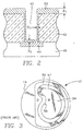
- a conventional PVD reactor 10 is illustrated schematically in cross section in FIG. 1, and the illustration is based upon the Endura PVD Reactor available from Applied Materials, Inc. of Santa Clara, California.
- the reactor 10 includes a vacuum chamber 12 sealed to a PVD target 14 composed of the material, usually a metal, to be sputter deposited on a wafer 16 held on a heater pedestal 18.
- a shield 20 held within the chamber protects the chamber wall 12 from the sputtered material and provides the anode grounding plane.
- a selectable DC power supply 22 negatively biases the target 14 to about -600VDC with respect to the shield 20.
- the pedestal 18 and hence the wafer 16 are left electrically floating.
- a gas source 24 supplies a sputtering working gas, typically the chemically inactive gas argon, to the chamber 12 through a mass flow controller 26.
- a sputtering working gas typically the chemically inactive gas argon
- nitrogen is supplied from another gas source 27 through its own mass flow controller 26.
- Oxygen can also be supplied to produce oxides such as Al 2 O 3 .
- the gases can be admitted to the top of the chamber, as illustrated, or at its bottom, either with one or more inlet pipes penetrating the bottom of the shield or through the gap between the shield 20 and the pedestal 18.
- a vacuum system 28 maintains the chamber at a low pressure. Although the base pressure can be held to about 10 -7 Torr or even lower, the pressure of the working gas is typically maintained at between about 1 and 1000m Torr.
- a computer-based controller 30 controls the reactor including the DC power supply 22 and the mass flow controllers 26.
- the DC voltage between the target 14 and the shield 20 ignites the argon into a plasma, and the positively charged argon ions are attracted to the negatively charged target 14.
- the ions strike the target 14 at a substantial energy and cause target atoms or atomic clusters to be sputtered from the target 14.
- Some of the target particles strike the wafer 16 and are thereby deposited on it, thereby forming a film of the target material.
- nitrogen is additionally admitted into the chamber 12, and it reacts with the sputtered metallic atoms to form a metallic nitride on the wafer 16.
- a magnetron 32 is positioned in back of the target 14. It has opposed magnets 34, 36 creating a magnetic field within the chamber in the neighborhood of the magnets 34, 36. The magnetic field traps electrons and, for charge neutrality, the ion density also increases to form a high-density plasma region 38 within the chamber adjacent to the magnetron 32.
- the magnetron 32 is usually rotated about the center of the target 14 to achieve full coverage in sputtering of the target 14.
- the form of the magnetron is a subject of this patent application, and the illustrated form is intended to be only suggestive.
- via or contact holes 40 are etched through an interlevel dielectric layer 42 to reach a conductive feature 44 in the underlying layer or substrate 46. Sputtering is then used to fill metal into the hole 40 to provide inter-level electrical connections. If the underlying layer 46 is the semiconductor substrate, the filled hole 40 is called a contact; if the underlying layer is a lower-level metallization level, the filled hole 40 is called a via. For simplicity, we will refer hereafter only to vias.
- inter-level vias have decreased to the neighborhood of 0.25 ⁇ m and below while the thickness of the inter-level dielectric has remained nearly constant at around 0.7 ⁇ m.
- the via holes in advanced integrated circuits have increased aspect ratios of three and greater.
- aspect ratios of six and even greater are required.
- Such high aspect ratios present a problem for sputtering because most forms of sputtering are not strongly anisotropic, a cosine dependence off the vertical being typical, so that the initially sputtered material preferentially deposits at the top of the hole and may bridge it, thus preventing the filling of the bottom of the hole and creating a void in the via metal.
- ionized metal deposition The process of sputtering with a significant fraction of ionized sputtered atoms is called ionized metal deposition or ionized metal plating (IMP).
- IMP ionized metal plating
- Two related quantitative measures of the effectiveness of hole filling are bottom coverage and side coverage.
- the initial phase of sputtering deposits a layer 50, which has a surface or blanket thickness of s 1 , a bottom thickness of s 2 , and a sidewall thickness of s 3 .
- the bottom coverage is equal to s 2 /s 1
- the sidewall coverage is equal to s 3 /s 1 .
- the model is overly simplified but in many situations is adequate.
- HDP high-density plasma
- An HDP reactor not only creates a high-density argon plasma but also increases the ionization fraction of the sputtered atoms.
- HDP PVD reactors are new and relatively expensive, and the quality of the deposited films is not always the best. It is desired to continue using the principally DC sputtering of the PVD reactor of FIG. 1.
- Another method for increasing the ionization ratio is to use a hollow-cathode magnetron in which the target has the shape of a top hat. This type of reactor, though, runs very hot and the complexly shaped targets are very expensive.
- variable thickness is particularly serious when the sputtered copper layer is being used as a seed layer of a predetermined minimum thickness for a subsequent deposition process such as electroplating to complete the copper hole filling.
- a further problem in the prior art is that the sidewall coverage tends to be asymmetric with the side facing the center of the target being more heavily coated than the more shielded side facing a larger solid angle outside the target. Not only does the asymmetry require excessive deposition to achieve a seed layer of predetermined minimum thickness, it causes cross-shaped trenches used as alignment indicia in the photolithography to appear to move as the trenches are asymmetrically narrowed.
- chamber pressure Another operational control that promotes deep hole filling is chamber pressure. It is generally believed that lower chamber pressures promote hole filling. At higher pressures, there is a higher probability that sputtered particles, whether neutral or ionized, will collide with atoms of the argon carrier gas. Collisions tend to neutralize ions and to randomize velocities, both effects degrading hole filling. However, as described before, the sputtering relies upon the existence of a plasma at least adjacent to the target. If the pressure is reduced too much, the plasma collapses, although the minimum pressure is dependent upon several factors.
- SSS sustained self-sputtering
- the density of positively ionized sputtered atoms is so high that a sufficient number are attracted back to the negatively biased target to resputter more ionized atoms.
- the self-sputtering sustains the plasma, and no argon working gas is required.
- Copper is the metal most prone to SSS, but only under conditions of high power and high magnetic field. Copper sputtering is being seriously developed because of copper's low resistivity and low susceptibility to electromigration.
- a full-coverage, high-field magnetron needs to be developed.
- Increased power applied to the target allows reduced pressure, perhaps to the point of sustained self-sputtering.
- the increased power also increases the ionization density.
- excessive power requires expensive power supplies and increased cooling. Power levels in excess of 20 to 30kW are considered infeasible in a commercial environment.
- the pertinent factor is not power but the power density in the area below the magnetron since that is the area of the high-density plasma promoting effective sputtering.
- a small, high-field magnet would most easily produce a high ionization density. For this reason, some prior art discloses a small circularly shaped magnet.
- magnetron requires not only rotation about the center of the target to provide uniformity, but it also requires radial scanning to assure full and fairly uniform coverage of the target. If full magnetron coverage is not achieved, not only is the target not efficiently used, but more importantly the uniformity of sputter deposition is degraded, and some of the sputtered material redeposits on the target in areas that are not being sputtered. Furthermore, the material redeposited on unsputtered areas may build up to such a thickness that it is prone to flake off, producing severe particle problems. While radial scanning can potentially avoid these problems, the required scanning mechanisms are complex and generally considered infeasible in a production environment.
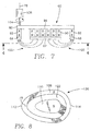
- the Tepman magnetron 52 is based on a kidney shape for the magnetically opposed pole faces 54, 56 separated by a circuitous gap 57 of nearly constant width.
- the pole faces 54, 56 are magnetically coupled by unillustrated horseshoe magnets bridging the gap 57.
- the magnetron rotates about a rotational axis 58 at the center of the target 14 and near the concave edge of the kidney-shaped inner pole face 54.
- the convexly curved outer periphery of the outer pole face 56 which is generally parallel to the gap 57 in that area, is close to the outer periphery of the usable portion if the target 14.
- This shape has been optimized for high field and for uniform sputtering but has an area that is nearly half that of the target. It is noted that the magnetic field is relatively weak in areas separated from the pole gap 57.
- the invention includes a sputtering magnetron having an oval or related shape of smaller area than a circle of equal diameter where the two diameters extend along the target radius with respect to the typical rotation axis of the magnetron.
- the shapes include racetracks, ellipses, egg shapes, triangles, and arced triangles asymmetrically positioned about the target center.
- the magnetron is rotated on the backside of the target about a point preferably near the magnetron's thin end, and the thicker end is positioned more closely to the target periphery.
- the total magnetic flux is greater outside than inside the half radius of the target.
- the small area allows an electrical power density of at least 600W/cm 2 to be applied from an 18kW power supply to a fully covered sputtering target used to sputter deposit a 200mm wafer.
- the magnetron is configured to produce less magnetic flux in its inner pole than in its surrounding outer pole. Thereby, the magnetic field reaches further into the sputtering chamber to promote low-pressure sputtering and sustained self-sputtering.
- the invention also includes sputtering methods achievable with such a magnetron.
- the high magnetic field extending over a small closed area facilitates sustained self-sputtering.
- Many metals not subject to sustained self-sputtering can be sputtered at chamber pressures of less than 0.5 milliTorr, often less than 0.2 milliTorr, and even at 0.1 milliTorr.
- the bottom coverage can be further improved by applying an RF bias of less than 250W to a pedestal electrode sized to support a 200mm wafer. Copper can be sputtered with 18kW of DC power for a 330mm target and 200mm wafer either in a fully self-sustained mode or with a minimal chamber pressure of 0.3 milliTorr or less.
- the invention provides for high-power density sputtering with power supplies of reduced capacity.
- FIG. 1 is a schematic diagram of a DC plasma sputtering reactor.
- FIG. 2 is a cross-sectional view of a inter-level via in a semiconductor integrated circuit.
- FIG. 3 is a plan view of a conventional magnetron.
- FIG. 4 is a plan view of the pole pieces of an embodiment of the magnetron of the invention taken along the view line 4-4 of FIG. 7.
- FIG. 5 is a plan view of the magnets used in the magnetron of FIG. 4.
- FIG. 6 is a cross-sectional view of one of the magnets used in conjunction with the embodiments of the invention.
- FIG. 7 is a cross-sectional view of the magnetron of FIG. 4.
- FIG. 8 is a plan view of an egg-shaped magnetron.
- FIG. 9 is a plan view of a triangularly shaped magnetron.
- FIG. 10 is a plan view of a modification of the triangularly shaped magnetron of FIG. 9, referred to as an arced triangular magnetron.
- FIG. 11 is a plan view of the magnets used in the arced triangular magnetron of FIG. 10.
- FIG. 12 is a plan view of two model magnetrons used to calculate areas and peripheral lengths.
- FIG. 13 is a graph of the angular dependences of the areas of a triangular and of a circular magnetron.
- FIG. 14 is a graph of the angular dependences of the peripheral lengths of the two types of magnetrons of FIG. 12.
- FIG. 15 is a side view of an idealization of the magnetic field produced with the described embodiments of the invention.
- FIG. 16 is a graph showing the effect of RF wafer bias in bottom coverage in titanium sputtering.
- FIG. 17 is a graph of the dependence of chamber pressure upon nitrogen flow illustrating the two modes of deposition obtained in reactive sputtering of titanium nitride with a magnetron of the invention.
- FIG. 18 is a graph of the step coverage obtained in the two sputtering modes for reactive sputtering of titanium nitride with a magnetron of the invention.
- the racetrack magnetron 60 has a central bar-shaped pole face 62 of one magnetic polarity having opposed parallel middle straight sides 64 connected by two rounded ends 66.
- the central, bar-shaped pole face 62 is surrounded by an outer elongated ring-shaped pole face 68 of the other polarity with a gap 70 of nearly constant width separating the bar-shaped and ring-shaped pole faces 62, 68.
- the outer pole face 68 of the other magnetic polarity includes opposed parallel middle straight sections 72 connected by two rounded ends 74 in general central symmetry with the inner pole face 62.
- the middle sections 72 and rounded ends 74 are bands having nearly equal widths.
- Magnets cause the pole faces 62, 68 to have opposed magnetic polarities.
- a backing plate also to be described shortly, provides both a magnetic yoke between the magnetically opposed pole faces 62, 68 and support for the magnetron structure.
- the illustrated assembly produces a generally semi-toroidal magnetic field having parallel arcs extending perpendicularly to a closed path with a minimal field-free region in the center. There results a closed tunnel of magnetic field forming struts of the tunnel.
- the pole assembly of FIG. 4 is intended to be continuously rotated during sputter deposition at a fairly high rotation rate about a rotation axis 78 approximately coincident with the center of the target 14 of uniform composition.
- the rotation axis 78 is located at or near one prolate end 80 of the outer pole face 68 and with its other prolate end 82 located approximately at the outer radial usable extent of the target 14.
- the asymmetric placement of the rotating magnetron 60 with respect to the target center provides a small magnetron nonetheless achieving full target coverage.
- the outer usable periphery of the target is not easily defined because different magnetron designs use different portions of the same target.
- Racetrack magnetrons are well known in the prior art, but they are generally positioned symmetrically about the center of the target. In the described invention, the racetrack is asymmetrically positioned with its inner end either overlying the target center or terminating at a radial position preferably within 20% and more preferably within 10% of the target radius from the target center. The illustrated racetrack extends along a diameter of the target.
- two sets of magnets 90, 92 are disposed in back of the pole faces 62, 68 to produce the two magnetic polarities.
- the combination of the pole faces 62, 68, the magnets 90, 92, and possibly a back magnetic yoke produces two opposite magnetic poles having areas defined by the pole faces 62, 68.
- Other means may be used to achieved such poles.
- the two types of magnets 90, 92 may be of similar construction and composition producing an axially extending magnetic flux on each vertically facing end. If they are of different, magnetic composition, diameter, or length, the flux produced by different magnets may be different.
- a cross-sectional view of a magnet 90, 92 is shown in FIG. 6.
- a cylindrical magnetic core 93 extending along an axis is composed of a strongly magnetic material, such as neodymium boron iron (NdBFe). Because such a material is easily oxidized, the core 93 is encapsulated in a case made of a tubular sidewall 94 and two generally circular caps 96 welded together to form an air-tight canister.
- the caps 96 are composed of a soft magnetic material, preferably SS410 stainless steel, and the tubular sidewall 96 is composed of a non-magnetic material, preferably SS304 stainless steel.
- Each cap 96 includes an axially extending pin 97, which engages a corresponding capture hole in one of the pole faces 62, 68 or in a magnetic yoke to be shortly described.
- the magnets 90, 92 are fixed in the magnetron.
- the magnetic core 93 is magnetized along its axial direction, but the two different types of magnets 90, 92 are oriented in the magnetron 60, as illustrated in the cross-sectional view of FIG.
- the magnets 90, 92 are arranged closely above (using the orientation of FIG. 1) the pole faces 62, 68 located just above the back of the target 14.
- a magnetic yoke 98 having a generally closed shape generally conforming to the outer periphery of the outer pole face 68 is closely positioned in back of the magnets 90, 92 to magnetically couple the two poles 62, 68.
- holes in the pole faces 62, 68 and in the yoke 98 fix the magnets 90, 92, and unillustrated hardware fix the pole faces 62, 68 to the yoke 98.
- the inner magnets 90 and inner pole face 62 constitute an inner pole of one magnetic polarity while the outer magnets 92 and the outer pole face 68 constitute a surrounding outer pole of the other magnetic polarity.
- the magnetic yoke 98 magnetically couples the inner and outer poles and substantially confines the magnetic field on the back or top side of the magnetron to the yoke 98.
- a semi-toroidal magnetic field 100 is thereby produced, which extends through the non-magnetic target 14 into the vacuum chamberl2 to define the high-density plasma region 38.
- the field 100 extends through the non-magnetic target 14 into the vacuum chamber 12 to define the extent of the high-density plasma region 38.
- the magnets 90, 92 may be of different magnetic strength.
- the total magnetic flux produced by the outer magnets 92 be substantially greater than that produced by the inner magnets 90.
- the magnetron 60 extends horizontally from approximately the center of the target 14 to the edge of the usable area of the target 14.
- the magnetic yoke 90 and the two pole faces 62, 68 are preferably plates formed of a soft magnetic material such as SS416 stainless steel.
- the inner prolate end 80 of the magnetron 60 is connected to a shaft 104 extending along the rotation axis 78 and rotated by a motor 106. As illustrated, the magnetron 60 extends horizontally from approximately the center of the target 14 to the right hand side of the usable area of the target 14.
- Demaray et al. in U.S. Patent 5,252,194 disclose exemplary details of the connections between the motor 106, the magnetron 60, and the vacuum chamber 12.
- the magnetron assembly 60 should include counter-weighting to avoid flexing of the shaft 104.
- center of rotation 78 is preferably disposed within the inner prolate end 74 of the outer pole face 72, its position may be optimized to a slightly different position, but one preferably not deviating more than 20%, more preferably 10%, from the inner prolate end 80 as normalized to the prolate length of the magnetron 60. Most preferably, the inner end of the outer pole face 68 near the prolate end 80 overlies the rotation center 78.
- the racetrack configuration of FIG. 4 has the advantage of simplicity and a very small area while still providing full target coverage.
- the asymmetric magnetic flux of the two poles is advantageous for low-pressure sputtering and sustained self-sputtering.
- the racetrack configuration of FIG. 4 can be alternatively characterized as an extremely flattened oval.
- Other oval shapes are also included within the invention, for example, continuously curved shapes of continuously changing diameter such as elliptical shapes with the major axis of the ellipse extending along the radius of the target and with the minor axis preferably parallel to a rotational circumference.
- Tabuchi illustrates a symmetric oval magnetron in Laid-open Japanese Patent Application 63-282263. This shape however has the disadvantage of a complex shape, especially for packing the magnets in the inner pole.
- FIG. 8 Another oval shape is represented by an egg-shaped magnetron 106, illustrated in plan view in FIG. 8. It has an outer pole face 108 of one magnetic polarity surrounding an inner pole face 110 of the other polarity with a nearly constant gap 122 between them. Both pole faces 108, 110 are shaped like the outline of an egg with a major axis extending along the radius of the target. However, an inner end 112 of the outer pole face 108 near the rotation axis 78 is sharper than an outer end 114 near the periphery of the target.
- the egg shape is related to an elliptical shape but is asymmetric with respect to the target radius. Specifically, the minor axis is pushed closer to the target periphery than its center.
- the inner pole face 110 and the gap 122 are similarly shaped. Such an egg shape places more of the magnetic flux closer to the target periphery so as to improve sputtering uniformity.
- Such a preferred flux distribution may be chara cterized with respect to the half radius of the target extending from its center to its outer usable radius.
- the total magnetic flux located outside the half radius is greater than that located inside the half radius, for example, by at least a 3:2 ratio, and preferably between 1.8 and 2.3.
- the ratio of magnetic flux outside to inside the target half radius in this configuration is about 2:1.
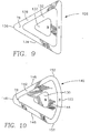
- a related shape is represented by a triangular magnetron 126, illustrated in plan view in FIG. 9. It has a triangular outer pole face 128 of one magnetic polarity surrounding a substantially solid inner pole face 130 of the other magnetic polarity with a gap 132 between them.
- the triangular shape of the inner pole face 130 with rounded comers allows hexagonal close packing of the button magnets 90, 92 of FIG. 6.
- the outer pole face 128 has three straight sections 134 are preferably offset by 60° with respect to each other and are connected by rounded corners 136. Preferably, the rounded corners 136 have smaller lengths than the straight sections 134.
- One rounded corner 136 is located near the rotation center 78 and target center, preferably within 20%, more preferably within 10% of the target radius, and most preferably with the apex portion of the outer pole face 128 overlying the rotation center 78.
- the triangularly shaped inner pole piece 130 may include a central aperture, but it is preferred that the size of such an aperture be kept small to minimize the size of the central magnetic cusp.
- a modified triangular shape is represented by an arced triangular magnetron 140 of FIG. 10. It includes the triangular inner pole face 130 surrounded by an arced triangular outer pole face 142 with a gap 144 between them and between the magnets of the respective poles and with the magnetic yoke in back of the gap 144.
- the outer pole face 142 includes two straight sections 146 connected to each other by a rounded apex comer 148 and connected to an arc section 150 by rounded circumferential corners 152.
- the apex corner 148 is placed near the rotational center 78 and the target center, preferably within 20% and more preferably within 10% of the target radius.
- the arc section 150 is located generally near the circumferential periphery of the target.
- It curvature may be equal to that of the target, that is, be equidistant from the center of rotation 78, but other optimized curvatures may be chosen for an arc section concave with respect to the rotational center 78. It is located near the target periphery within the chamber, preferably within 25% and more preferably within 15% of the radius to the periphery.
- Yokoyama et al. in Laid-open Japanese Patent Application 62-89864 discloses the advantage of a plurality of arced triangular magnetrons arranged symmetrically about the target center. However, plural magnetrons do not provide for a small total area and thus do not achieve a high power density for sputtering. Furthermore, the apices of the individual magnetron sections in Yokoyama are located relatively far from the target center, thus producing poor sputtering uniformity except for a large number of sections.
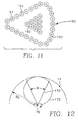
- the magnetic field is produced by an arrangement of magnets shown in plan view in FIG. 11. Magnets 160 of a first polarity are disposed adjacent to the inner pole face 130 in an advantageous hexagonally close-packed arrangement. Magnets 162 of a second polarity are arranged adjacent to the arc section 150 of the outer pole face 142 while magnets 164 of the second polarity are arranged adjacent to the remaining portions of the outer pole face 142. In some situations, to be described later, it is advantageous to place magnets of different intensities at different portions of the outer pole face 142. In one embodiment, there are 10 magnets in the inner pole and 26 magnets in the outer pole, which for magnets of equal strength produces 2.6 more magnetic flux in the outer pole than in the inner pole.
- the triangular magnetrons 126, 140 of FIGS. 9 and 10 are illustrated as having apex angles ⁇ of 60°, which facilitates promotes hexagonal close packing of the button magnets, but the apex angle can be changed, in particular decreased below 60°. However, 60° ⁇ 15° seems to provide superior uniformity.
- the apex angle significantly affects two important parameters of the magnetron of the invention, the values of its area A and its perimeter P .
- a simplified or model arced triangular magnetron 170 has two straight sides extending between the center and periphery of the target 14 of radius R T and meeting at an apex coincident with the rotation axis 78 and further includes an arc side conforming to the usable periphery of the target 14.
- the area A of the simplified arced triangular magnetron 170 is ⁇ R T 2 /2, and its periphery P is R T (2+ ⁇ ), where ⁇ is measured in radians.
- a model circular magnetron 172 having a radius of R T /2 and having a diameter fixed to the rotation axis 78.
- Ionization efficiency is increased by minimizing the area, since the target power is concentrated in a smaller area, and is also increased by minimizing the periphery, since edge loss is generally proportional to the peripheral length.
- the area needs to be large enough to accommodate the magnets creating the magnetic field. Also, these calculations do not address uniformity. It is likely that the circular magnetron 170 provides reduced uniformity relative to the arced triangular magnetron 172.
- the ratio of the magnetic flux outside to inside the target half radius for the arced triangular magnetron 172 can be approximated by the lengths of the sides 170 in the two regions by (1+ ⁇ ), which is 1.79 for an apex angle ⁇ of 45°, 2.05 for 60°, 2.31 for 75°, and 2.57 for 90°.
- a variation of the arced triangular arrangement of FIGS. 10 and 11 decreases the apex angle to, for example, 47°.
- one or more inner magnets are linearly arranged from the inner corner of hexagonally closed packed magnets toward the inner corner of the outer magnets 164. The result is intermediate the racetrack magnetron and the arced triangular magnetron
- the shapes described above refer to pole faces having band-like widths of area not significantly larger than the button magnets being used.
- the widths, particularly of the outer pole face, can be increased, perhaps even non-uniformly, but the additional width is of less effectiveness in generating the desired high magnetic field.
- the magnetron of the invention includes asymmetric shapes, for example one radially extending side being in the form of the racetrack of FIG. 4 and the other side being oval, e.g., the egg shape of FIG. 7, or one radially extending side being oval or straight and the other side having a triangular apex between the center and periphery of the target.
- All the magnetrons described above have asymmetric areas for the inner and outer poles and, assuming similar packing of similar button magnets 90, 92, asymmetric magnetic flux.
- the total magnetic flux ⁇ B ⁇ dS produced by the inner pole 190, illustrated schematically in FIG. 15, is much less than that produced by the surrounding outer pole 192, for example, by at least a factor of 1.5 and preferably 2.
- All the magnetrons are also characterized as having a compact inner pole 190 surrounded by the outer pole 192.
- the result is a magnetic field distribution which is very strong in the reactor processing area 194 adjacent to the gap 196 between the poles 190, 192, but which also extends far into the processing area 194 as the magnetic field lines of the outer pole 192 close back to the magnetic yoke 198.
- the substantial fraction of magnetic field extending vertically from the target deep into the processing area 194 offers many advantages. Because the light electrons orbit around magnetic field lines, the extended magnetic field traps electrons and thus helps to support a higher-density plasma deep into the processing area 194. By the same interaction, the magnetic field extending close and parallel to the grounded chamber shield reduces electron loss to the shield, also increasing the density of the plasma. As a result, the plasma can be supported at lower pressure or even be self-sustained. The magnetic field also partially traps heavier positive particles and thus guides ionized sputtered particles towards the wafer.
- the inventive magnet also achieves a relatively high magnetic field.
- magnetic field intensity of itself is insufficient.
- a relatively high magnetic field intensity can be achieved in the area at the periphery of the kidney shape.
- the linear shape of the high magnetic field surrounds an area of substantially no magnetic field.
- electrons can escape to not only the exterior but also the interior of the high-field region.
- the inner pole of the triangular magnetron of the invention produces a magnetic cusp of minimal area.
- the inner pole includes a single magnetizable pole face producing a generally uniform magnetic flux. If multiple inner poles faces were used for multiple inner magnets, magnetic field lines would extend to between the inner magnets.
- a further advantage of the inventive design is that one pole is formed in a closed line and surrounds the other pole. It would be possible to form a very small linearly extending magnetron with high magnetic field intensity by arranging horseshoe magnets or the like in an open ended line with the two sets of poles being closely spaced. However, the electrons could then easily escape from the open ends and decrease the density of the plasma.
- the inventive magnetron has a relatively small area, but has a shape that allows full target coverage without radial scanning.
- the triangular magnetron 160 of FIG. 10 with an apex angle of 60° has an area of 1/6 (0.166) of the usable target area.
- the circular magnetron 162 were used, which similarly extends from the target center to the periphery, the magnetron area is 1/4 (0.25) of the target area.
- the power density is less for a given power supply powering a larger circular magnetron.
- the target overlay percentage is even higher for the Tepman magnet of FIG. 3.
- the combination of small area and full coverage is achieved by an outer magnetron shape extending from the target center to its usable periphery ( ⁇ 15%) and having a transverse dimension at half the target radius of less substantially less than the target radius, that is, prolate along the target radius.
- the transverse dimension should be measured circumferentially along the rotation path.
- the uniformity is enhanced by an oval shape that is transversely wider, with respect to the target radius, at its outer end near the target periphery than at its inner end near the center of rotation. That is, the minor axis is displaced towards the target circumference.
- the small area of the magnetron allows a very high power density to be applied to the target with a reasonably sized power supply.
- the small area unlike the Tepman design, has no substantial field-free region included in its interior. Some of the examples below use an 18kW power source.
- the magnetron extends out to a usable target diameter of about 300mm.
- the effective area of the arced triangular magnetron is about one-sixth of the area associated with this larger diameter, that is, about 117cm 2 .
- the average power density of the area being sputtered at any given location of the magnetron is about 150W/cm 2 .
- Such a high power density achieved without inductive coils can support a plasma at lower argon pressure or permit sustained self-sputtering for selected metals such as copper.
- a 27kW power supply in conjunction with the small magnetron of the invention scaled to the larger dimension will produce a target power density of 103W/cm 2 .
- a power density of 76W/cm 2 is sufficient for sustained self-sputtering of copper.
- a racetrack magnetron of FIGS. 4 and 5 was tested with copper sputtering.
- six magnets 90 are placed behind the center pole face 62, twenty-five magnets of the same strength but opposite polarity are arranged behind and around the outer pole face 68, and the spacing between the 33cm target and the 200mm wafer is 190mm. This configuration produces a deposition uniformity of ⁇ 18%.
- the magnets In a second configuration, the magnets have different strengths, the stronger ones producing 30% more magnetic flux.
- Six strong magnets are placed behind the center pole face, and 25 weaker magnets are placed around the outer pole face. Despite the stronger inner magnets, the total magnetic flux produced by the outer magnets is greater than that produced by the inner ones.
- the second configuration produces an improved deposition uniformity of 8.9%.
- the second configuration also produces superior hole filling into a 0.5 ⁇ m-wide, 2 ⁇ m-deep via hole. For 265nm of blanket copper, the bottom coverage is between 10 and 15%, and the sidewall coverage is about 2.8%.
- the deep hole filling is promoted by the small area of the racetrack magnetron producing a higher ionization density.
- strong magnets replace some of the weaker magnets near the ends of the outer pole. This produces a somewhat better uniformity.
- FIGS. 10 and 11 An arced triangular magnetron of FIGS. 10 and 11 was tested in a series of experiments with different sputtering composition. For almost all the experiments, the target was spaced between 190 and 200mm from the wafer and the target had a diameter of 330mm for a 200mm wafer.
- uniformity is improved by using ten strong magnets 160 in the inner pole, strong magnets 162 along the arc portion 150 of the outer pole, and weaker magnets 164 for the remainder of the outer pole.
- the stronger magnets have a diameter 30% larger than the diameter of the weaker magnets, but are otherwise of similar composition and structure, thereby creating an integrated magnetic flux that is 70% larger.
- Sustained self-sputtering of copper is achieved, after striking the plasma in an argon ambient, with 9kW of DC power applied to the target having a usable diameter of about 30cm, which results in a power density of 76W/cm 2 with the arced triangular magnetron.
- the increased background pressure of 0.1 to 0.3 milliTorr enhances effective wafer cooling without significant increase in the scattering and deionization of the sputtered ions.
- These relatively low DC powers are important in view of the ongoing development of equipment for 300mm wafers, for which these numbers scale to 20kW and 40kW. A power supply of greater than 40kW is considered expensive if not infeasible.
- ionized copper sputtering is to deposit a thin conformal seed layer of copper in a deep and narrow via hole. Thereafter, electro or electroless plating can be used to quickly and economically fill the remainder of the hole with copper.
- a via hole having a top width of 0.30 ⁇ m and extending through 1.2 ⁇ m of silica was first coated with a Ta/TaN barrier layer.
- copper was deposited over the barrier layer at 18kW of target power and a pressure of 0.2 milliTorr. The deposition was carried out to a blanket thickness of about 0.15 ⁇ m.
- the sides of the via hole was smoothly covered.
- the experiments show that the sidewall thickness of the copper is about 7nm on one side and 11.4nm on the other side (5% and 8%) for a via located at the wafer edge.
- the bottom coverage is about 24nm (16%).
- Sidewall symmetry is improved for a via hole at the wafer center.
- the smoothness promotes the use of the deposited layer as a seed layer and as an electrode for subsequent electroplating of copper.
- the relatively good symmetry between the two sidewalls relieves the problem in the prior art of apparently moving photolithographic indicia.
- sputtering of an aluminum target was achieved at both 12kW and 18kW of applied power with a minimum pressure of about 0.1 milliTorr, a significant improvement.
- sidewall coverage and particularly bottom coverage is significantly improved.
- the better uniformity is also believed to be related in part to the increased ionization fraction since the self-biased pedestal supporting the wafer attracts the ionized sputtered particles across its entire area. It is estimated that the magnetron of the invention increases the ionization fraction from 2% to at least 20% and probably 25%.
- the arced triangular magnetron was compared under similar operating conditions to the operation of a conventional magnetron resembling the Tepman magnetron of FIG. 3.
- the comparative results are summarized in TABLE 1 for the sputtering of aluminum.
- the coverage results were obtained for via holes having a width of 0.25 ⁇ m and a depth of 1.2 ⁇ m, that is, an aspect ratio of about 5.
- the bottom coverage is significantly improved with the inventive triangular magnetron compared to the conventional magnetron.
- the sidewall coverage is also increased, and further the coverage is smooth and uniform from top to bottom. These two characteristics promote the use of the deposited metal layer as a seed layer for a subsequent deposition step. This is particularly important for copper in which the second deposition is performed by a different process such as electroplating.
- the increased bottom and sidewall coverages are believed to be due to the higher ionization fraction of sputtered aluminum atoms achieved with the inventive triangular magnetron. This ionization fraction is believed to be 25% or greater.
- the uniformity of blanket (planar) deposition was determined both for a separation of 190mm between the target and the wafer and, in a long-throw implementation, for a separation of 290mm.
- the inventive triangular magnetron produces better uniformity, especially for long throw.
- the better uniformity is also believed to be related to the increased ionization fraction since the self-biased pedestal supporting the wafer attracts the ionized sputtered particles across its entire area.
- the inventive triangular magnetron produces less asymmetry between the coverages of the two opposed sidewalls.
- the increased ionization density is due in part to the relatively small inner yoke having an area substantially less than that of the outer yoke. As a result, electrons lost from one side of the inner yoke are likely to be captured by the other side.
- Titanium sometimes in conjunction with titanium nitride, is useful in aluminum metallization for providing a silicided contact to silicon at the bottom of a contact hole and to act as wetting layer and in conjunction with a titanium nitride layer as a barrier both to the silicon in a contact hole and between the aluminum and the silica dielectric on the via or contact sidewalls. Conformal and relatively thick coatings are thus required.
- an RF power source 192 illustrated in FIG. 1, was connected to the heater pedestal 18 through a coupling capacitor circuit 194. It is known that such an RF field applied to the wafer adjacent to a plasma creates a DC self-bias.
- 100W of 400kHz power is applied with a chamber pressure of 0.3 milliTorr, the bottom coverage is significantly increased, as shown by line 196 in the graph of FIG. 16.
- the bias power is increased to 250W, resputtering and faceting of the top comers of the via hole becomes a problem.
- the bottom coverage results for 250W bias are shown by line 198.
- bias powers should be kept below 250W for lower bias frequencies of 2MHz or less.
- These powers should be normalized to a 200mm circular reference wafer.
- Other sizes of wafers, such as a 300mm wafer can be used, and these wafers may not be completely circularly because of indexing flats or notches.
- the same effects are expected when the power levels quoted above are referenced to a 200mm circular reference wafer and then scaled according to the differing area of a substantially circular working wafer.
- the magnetron of the invention can also be used for reactive sputtering, such as for TiN, in which nitrogen is additionally admitted into the chamber to react with the sputtered metal, for example, with titanium to produce TiN or with tantalum to produce TaN.
- Reactive sputtering presents a more complex and varied chemistry.
- Reactive sputtering to produce TiN is known to operate in two modes, metallic mode and poison mode.
- Metallic mode produces a high-density, gold-colored film on the wafer.
- Poison mode which is often associated with a high nitrogen flow, produces a purple/brown film which advantageously has low stress.
- the poison-mode film has many grain boundaries, and film defects severely reduce chip yield.
- the deposition rate in poison mode is typically only one-quarter of the rate in metallic mode. It is generally believed that in poison mode the nitrogen reacts with the target to form a TiN surface on the Ti target while in metallic mode the target surface remains clean and TiN forms only on the wafer.
- the arced triangular magnetron was tested for reactive sputtering of titanium nitride in the same chamber used for sputter depositing titanium.
- the initialization conditions for sputter depositing titanium nitride are found to be very important to obtain operation in the metallic mode.
- argon alone is first admitted to the chamber. After the plasma is struck at an argon pressure of about 0.5 milliTorr, the argon flow is reduced to 5sccm producing a pressure of 0.3 milliTorr.
- the nitrogen flow is then step wise ramped up to 100sccm and then is gradually reduced, the dependence of the chamber pressure upon the flow assumes a hysteretic form illustrated in FIG. 17. Between about 50 and 70 sccm of nitrogen, intermediate ramp-up pressures 200 are below corresponding intermediate ramp-down pressures 202.
- poison mode can be achieved by first going to the higher pressures 206 and then decreasing to the ramp-down intermediate pressures 202.
- poison mode can be achieved by immediately turning on the desired gas flow, but only gradually turning on the DC sputtering power supply at a rate of no more than 5kW/s.
- Titanium nitride was sputtered into high aspect-ratio via holes in both metallic and poison modes at a N 2 flow of 50 sccm and an Ar flow of 5 sccm after the plasma had been struck in argon. These flows produce a pressure of 1.7 milliTorr in metallic mode and 2.1 milliTorr in poison mode.
- the deposition rates are 100nm/min in metallic mode and 30nm/min in poison mode.
- the TiN film stress is higher when it is deposited in metallic mode, but on the other hand poison mode suffers from overhang and undulatory sidewall thicknesses near the top of the via hole.
- a series of experiments deposited TiN into via holes of differing aspect ratios.
- the resulting measured bottom coverage illustrated in the graph of FIG. 18, shows in line 210 that bottom coverage in metallic mode remains relatively high even with an via aspect ratio of 5 while in line 212 the step coverage in poison mode is always lower and drops dramatically for aspect ratios of four and higher. However, when additionally the wafer is biased, step coverage of TiN deposited in the poison mode is acceptable.
- the barrier layer consisted of 30nm of Ti covered by 30nm of TiN deposited with the arced magnetron of the invention in an otherwise conventional non-inductive sputter reactor. Following the Ti/TiN deposition, the chip was subjected to rapid thermal processing (RTP) in which intense radiant lamps quickly heat the wafer surface for a short period.
- RTP rapid thermal processing
- the barrier layer consisted of 30nm of Ti covered by 10nm of TiN deposited as in the first series. However, in the second test, before the Ti/TiN deposition the wafer was subjected to a plasma preclean, but there was no RTP afterwards. In either case, tungsten was then CVD deposited over the Ti/TiN.
- the Ti/TiN process performed with the magnetron of the invention can be successfully integrated into a tungsten plug process.
- the inventive magnetron can also be used to sputter deposit other materials, for example, W, using a tungsten target, or TaN, using a tantalum target and nitrogen gas in the plasma. Reactive sputtering of WN is also contemplated.
- the magnetron of the invention is thus efficient in producing a high ionization fraction because of the high-density plasma it can create without excessive power being required. Nonetheless, its full coverage allows for uniform deposition and full target utilization. Its sputtering uniformity is good. Nonetheless, no complex mechanisms are required.
- the effectiveness of the magnetron of the invention in providing high-performance full-coverage sputtering is based on three interrelated synergetic effects.
- the magnetron has a small magnetic area. Thereby, the average magnetic field can be made high, and the plasma losses reduced.
- the small magnetron also allows a high average power density to be applied to the area of the target beneath the magnetron. That is, although the electrical power applied to the target as a whole is relatively modest, the electrical power density and resulting plasma density in the area actually being sputtered at any instant is high.
- the asymmetry of the inner and outer magnetic poles of the magnetron produces portions of the magnetic field extending vertically surrounding the periphery of the magnetron and extending far into the chamber.
- This magnetic field distribution reduces plasma losses and guides ionized sputtered particles to the substrate. All of these advantages are enjoyed in a magnetron providing full coverage sputtering of the target with only circumferential scanning, and in a magnetron that can be optimally shaped to produce uniform target sputtering and uniform substrate deposition.
- Such a small, high-field magnet enables sustained self-sputtering with relatively modest target power and also enables sputtering of materials such as aluminum and titanium at reduced pressures below 0.5 milliTorr, preferably below 0.2 milliTorr, and even at 0.1 milliTorr. At these pressures, deep hole filling can be facilitated by the reduced scattering of sputtered particles, whether neutral or ionized, and by the reduced neutralization of ionized particles.
- the magnetron of the invention deposition rate and bottom coverage are improved with working gas pressures above 0.7 milliTorr.
- the high-field magnet further promotes a high ionization fraction, which can be drawn into a deep, narrow hole by biasing of the wafer within proper ranges.
- magnetron of the invention can also be advantageously used in other types of sputter reactors, such as an HDP reactor relying upon inductively coupled RF power.
Abstract
Description
- The invention relates generally to sputtering of materials. In particular, the invention relates to the magnetron creating a magnetic field to enhance sputtering.
- Sputtering, alternatively called physical vapor deposition (PVD), is the most prevalent method of depositing layers of metals and related materials in the fabrication of semiconductor integrated circuits. A
conventional PVD reactor 10 is illustrated schematically in cross section in FIG. 1, and the illustration is based upon the Endura PVD Reactor available from Applied Materials, Inc. of Santa Clara, California. Thereactor 10 includes avacuum chamber 12 sealed to aPVD target 14 composed of the material, usually a metal, to be sputter deposited on awafer 16 held on aheater pedestal 18. Ashield 20 held within the chamber protects thechamber wall 12 from the sputtered material and provides the anode grounding plane. A selectableDC power supply 22 negatively biases thetarget 14 to about -600VDC with respect to theshield 20. Conventionally, thepedestal 18 and hence thewafer 16 are left electrically floating. - A
gas source 24 supplies a sputtering working gas, typically the chemically inactive gas argon, to thechamber 12 through amass flow controller 26. In reactive metallic nitride sputtering, for example, of titanium nitride, nitrogen is supplied from anothergas source 27 through its ownmass flow controller 26. Oxygen can also be supplied to produce oxides such as Al2O3. The gases can be admitted to the top of the chamber, as illustrated, or at its bottom, either with one or more inlet pipes penetrating the bottom of the shield or through the gap between theshield 20 and thepedestal 18. Avacuum system 28 maintains the chamber at a low pressure. Although the base pressure can be held to about 10-7Torr or even lower, the pressure of the working gas is typically maintained at between about 1 and 1000m Torr. A computer-basedcontroller 30 controls the reactor including theDC power supply 22 and themass flow controllers 26. - When the argon is admitted into the chamber, the DC voltage between the
target 14 and theshield 20 ignites the argon into a plasma, and the positively charged argon ions are attracted to the negativelycharged target 14. The ions strike thetarget 14 at a substantial energy and cause target atoms or atomic clusters to be sputtered from thetarget 14. Some of the target particles strike thewafer 16 and are thereby deposited on it, thereby forming a film of the target material. In reactive sputtering of a metallic nitride, nitrogen is additionally admitted into thechamber 12, and it reacts with the sputtered metallic atoms to form a metallic nitride on thewafer 16. - To provide efficient sputtering, a
magnetron 32 is positioned in back of thetarget 14. It has opposedmagnets magnets magnetron 32. Themagnetron 32 is usually rotated about the center of thetarget 14 to achieve full coverage in sputtering of thetarget 14. The form of the magnetron is a subject of this patent application, and the illustrated form is intended to be only suggestive. - The advancing level of integration in semiconductor integrated circuits has placed increasing demands upon sputtering equipment and processes. Many of the problems are associated with contact and via holes. As illustrated in the cross-sectional view of FIG. 2, via or
contact holes 40 are etched through an interleveldielectric layer 42 to reach aconductive feature 44 in the underlying layer orsubstrate 46. Sputtering is then used to fill metal into thehole 40 to provide inter-level electrical connections. If theunderlying layer 46 is the semiconductor substrate, the filledhole 40 is called a contact; if the underlying layer is a lower-level metallization level, the filledhole 40 is called a via. For simplicity, we will refer hereafter only to vias. The widths of inter-level vias have decreased to the neighborhood of 0.25µm and below while the thickness of the inter-level dielectric has remained nearly constant at around 0.7µm. As a result, the via holes in advanced integrated circuits have increased aspect ratios of three and greater. For some technologies under development, aspect ratios of six and even greater are required. - Such high aspect ratios present a problem for sputtering because most forms of sputtering are not strongly anisotropic, a cosine dependence off the vertical being typical, so that the initially sputtered material preferentially deposits at the top of the hole and may bridge it, thus preventing the filling of the bottom of the hole and creating a void in the via metal.
- It has become known, however, that deep hole filling can be facilitated by causing a significant fraction of the sputtered particles to be ionized in the plasma between the
target 14 and thepedestal 18. Thepedestal 18 of FIG. 1, even if it is left electrically floating, develops a DC self-bias, which attracts ionized sputtered particles from the plasma across the plasma sheath adjacent to thepedestal 18 and deep into thehole 40 in thedielectric layer 42. The effect can be accentuated with additional DC or RF biasing of thepedestal electrode 18 to additionally accelerate the ionized particles extracted across the plasma sheath towards thewafer 16, thereby controlling the directionality of sputter deposition. The process of sputtering with a significant fraction of ionized sputtered atoms is called ionized metal deposition or ionized metal plating (IMP). Two related quantitative measures of the effectiveness of hole filling are bottom coverage and side coverage. As illustrated schematically in FIG. 2, the initial phase of sputtering deposits alayer 50, which has a surface or blanket thickness of s1, a bottom thickness of s2, and a sidewall thickness of s3. The bottom coverage is equal to s2/s1, and the sidewall coverage is equal to s3/s1. The model is overly simplified but in many situations is adequate. - One method of increasing the ionization fraction is to create a high-density plasma (HDP), such as by adding an RF coil around the sides of the
chamber 12 of FIG. 1. An HDP reactor not only creates a high-density argon plasma but also increases the ionization fraction of the sputtered atoms. However, HDP PVD reactors are new and relatively expensive, and the quality of the deposited films is not always the best. It is desired to continue using the principally DC sputtering of the PVD reactor of FIG. 1. - Another method for increasing the ionization ratio is to use a hollow-cathode magnetron in which the target has the shape of a top hat. This type of reactor, though, runs very hot and the complexly shaped targets are very expensive.
- It has been observed that copper sputtered with either an inductively coupled HDP sputter reactor or a hollow-cathode reactor tends to form an undulatory copper film on the via sidewall, and further the deposited metal tends to dewet. The variable thickness is particularly serious when the sputtered copper layer is being used as a seed layer of a predetermined minimum thickness for a subsequent deposition process such as electroplating to complete the copper hole filling.
- A further problem in the prior art is that the sidewall coverage tends to be asymmetric with the side facing the center of the target being more heavily coated than the more shielded side facing a larger solid angle outside the target. Not only does the asymmetry require excessive deposition to achieve a seed layer of predetermined minimum thickness, it causes cross-shaped trenches used as alignment indicia in the photolithography to appear to move as the trenches are asymmetrically narrowed.
- Another operational control that promotes deep hole filling is chamber pressure. It is generally believed that lower chamber pressures promote hole filling. At higher pressures, there is a higher probability that sputtered particles, whether neutral or ionized, will collide with atoms of the argon carrier gas. Collisions tend to neutralize ions and to randomize velocities, both effects degrading hole filling. However, as described before, the sputtering relies upon the existence of a plasma at least adjacent to the target. If the pressure is reduced too much, the plasma collapses, although the minimum pressure is dependent upon several factors.
- The extreme of low-pressure plasma sputtering is sustained self-sputtering (SSS), as disclosed by Fu et al. in U.S. Patent Application, Serial No. 08/854,008, filed May 8, 1997. In SSS, the density of positively ionized sputtered atoms is so high that a sufficient number are attracted back to the negatively biased target to resputter more ionized atoms. Under the right conditions for a limited number of target metals, the self-sputtering sustains the plasma, and no argon working gas is required. Copper is the metal most prone to SSS, but only under conditions of high power and high magnetic field. Copper sputtering is being seriously developed because of copper's low resistivity and low susceptibility to electromigration. However, for copper SSS to become commercially feasible, a full-coverage, high-field magnetron needs to be developed.
- Increased power applied to the target allows reduced pressure, perhaps to the point of sustained self-sputtering. The increased power also increases the ionization density. However, excessive power requires expensive power supplies and increased cooling. Power levels in excess of 20 to 30kW are considered infeasible in a commercial environment. In fact, the pertinent factor is not power but the power density in the area below the magnetron since that is the area of the high-density plasma promoting effective sputtering. Hence, a small, high-field magnet would most easily produce a high ionization density. For this reason, some prior art discloses a small circularly shaped magnet. However, such a magnetron requires not only rotation about the center of the target to provide uniformity, but it also requires radial scanning to assure full and fairly uniform coverage of the target. If full magnetron coverage is not achieved, not only is the target not efficiently used, but more importantly the uniformity of sputter deposition is degraded, and some of the sputtered material redeposits on the target in areas that are not being sputtered. Furthermore, the material redeposited on unsputtered areas may build up to such a thickness that it is prone to flake off, producing severe particle problems. While radial scanning can potentially avoid these problems, the required scanning mechanisms are complex and generally considered infeasible in a production environment.
- One type of commercially available magnetron is kidney-shaped, as exemplified by Tepman in U.S. Patent 5,320,728. Parker discloses more exaggerated forms of this shape in U.S. Patent 5,242,566. As illustrated in plan view in FIG. 3, the
Tepman magnetron 52 is based on a kidney shape for the magnetically opposed pole faces 54, 56 separated by acircuitous gap 57 of nearly constant width. The pole faces 54, 56 are magnetically coupled by unillustrated horseshoe magnets bridging thegap 57. The magnetron rotates about arotational axis 58 at the center of thetarget 14 and near the concave edge of the kidney-shapedinner pole face 54. The convexly curved outer periphery of theouter pole face 56, which is generally parallel to thegap 57 in that area, is close to the outer periphery of the usable portion if thetarget 14. This shape has been optimized for high field and for uniform sputtering but has an area that is nearly half that of the target. It is noted that the magnetic field is relatively weak in areas separated from thepole gap 57. - For these reasons, it is desirable to develop a small, high-field magnetron providing full coverage so as to promote deep hole filling and sustained copper self-sputtering.
- The invention includes a sputtering magnetron having an oval or related shape of smaller area than a circle of equal diameter where the two diameters extend along the target radius with respect to the typical rotation axis of the magnetron. The shapes include racetracks, ellipses, egg shapes, triangles, and arced triangles asymmetrically positioned about the target center. The magnetron is rotated on the backside of the target about a point preferably near the magnetron's thin end, and the thicker end is positioned more closely to the target periphery. Preferably, the total magnetic flux is greater outside than inside the half radius of the target.
- The small area allows an electrical power density of at least 600W/cm2 to be applied from an 18kW power supply to a fully covered sputtering target used to sputter deposit a 200mm wafer.
- The magnetron is configured to produce less magnetic flux in its inner pole than in its surrounding outer pole. Thereby, the magnetic field reaches further into the sputtering chamber to promote low-pressure sputtering and sustained self-sputtering.
- The invention also includes sputtering methods achievable with such a magnetron. The high magnetic field extending over a small closed area facilitates sustained self-sputtering. Many metals not subject to sustained self-sputtering can be sputtered at chamber pressures of less than 0.5 milliTorr, often less than 0.2 milliTorr, and even at 0.1 milliTorr. The bottom coverage can be further improved by applying an RF bias of less than 250W to a pedestal electrode sized to support a 200mm wafer. Copper can be sputtered with 18kW of DC power for a 330mm target and 200mm wafer either in a fully self-sustained mode or with a minimal chamber pressure of 0.3 milliTorr or less.
- The invention provides for high-power density sputtering with power supplies of reduced capacity.
- The invention may be put into practice in a number of ways and one embodiment will now be described by way of example only and with reference to the accompanying Figures in which:
- FIG. 1 is a schematic diagram of a DC plasma sputtering reactor.
- FIG. 2 is a cross-sectional view of a inter-level via in a semiconductor integrated circuit.
- FIG. 3 is a plan view of a conventional magnetron.
- FIG. 4 is a plan view of the pole pieces of an embodiment of the magnetron of the invention taken along the view line 4-4 of FIG. 7.
- FIG. 5 is a plan view of the magnets used in the magnetron of FIG. 4.
- FIG. 6 is a cross-sectional view of one of the magnets used in conjunction with the embodiments of the invention.
- FIG. 7 is a cross-sectional view of the magnetron of FIG. 4.
- FIG. 8 is a plan view of an egg-shaped magnetron.
- FIG. 9 is a plan view of a triangularly shaped magnetron.
- FIG. 10 is a plan view of a modification of the triangularly shaped magnetron of FIG. 9, referred to as an arced triangular magnetron.
- FIG. 11 is a plan view of the magnets used in the arced triangular magnetron of FIG. 10.
- FIG. 12 is a plan view of two model magnetrons used to calculate areas and peripheral lengths.
- FIG. 13 is a graph of the angular dependences of the areas of a triangular and of a circular magnetron.
- FIG. 14 is a graph of the angular dependences of the peripheral lengths of the two types of magnetrons of FIG. 12.
- FIG. 15 is a side view of an idealization of the magnetic field produced with the described embodiments of the invention.
- FIG. 16 is a graph showing the effect of RF wafer bias in bottom coverage in titanium sputtering.
- FIG. 17 is a graph of the dependence of chamber pressure upon nitrogen flow illustrating the two modes of deposition obtained in reactive sputtering of titanium nitride with a magnetron of the invention.
- FIG. 18 is a graph of the step coverage obtained in the two sputtering modes for reactive sputtering of titanium nitride with a magnetron of the invention.
- One embodiment of the invention is a
racetrack magnetron 60, illustrated in plan view in FIG. 4. Theracetrack magnetron 60 has a central bar-shapedpole face 62 of one magnetic polarity having opposed parallel middlestraight sides 64 connected by two rounded ends 66. The central, bar-shapedpole face 62 is surrounded by an outer elongated ring-shapedpole face 68 of the other polarity with agap 70 of nearly constant width separating the bar-shaped and ring-shaped pole faces 62, 68. Theouter pole face 68 of the other magnetic polarity includes opposed parallel middlestraight sections 72 connected by two rounded ends 74 in general central symmetry with theinner pole face 62. Themiddle sections 72 and rounded ends 74 are bands having nearly equal widths. Magnets, to be described shortly, cause the pole faces 62, 68 to have opposed magnetic polarities. A backing plate, also to be described shortly, provides both a magnetic yoke between the magnetically opposed pole faces 62, 68 and support for the magnetron structure. - Although the two pole faces 62, 68 are illustrated with specific magnetic polarities producing magnetic fields extending generally perpendicularly to the plane of illustration, it is of course appreciated that the opposite set of magnetic polarities will produce the same general magnetic effects as far as the invention is concerned. The illustrated assembly produces a generally semi-toroidal magnetic field having parallel arcs extending perpendicularly to a closed path with a minimal field-free region in the center. There results a closed tunnel of magnetic field forming struts of the tunnel.
- The pole assembly of FIG. 4 is intended to be continuously rotated during sputter deposition at a fairly high rotation rate about a
rotation axis 78 approximately coincident with the center of thetarget 14 of uniform composition. Therotation axis 78 is located at or near oneprolate end 80 of theouter pole face 68 and with its otherprolate end 82 located approximately at the outer radial usable extent of thetarget 14. The asymmetric placement of the rotatingmagnetron 60 with respect to the target center provides a small magnetron nonetheless achieving full target coverage. The outer usable periphery of the target is not easily defined because different magnetron designs use different portions of the same target. However, it is bounded by the flat area of the target and almost always extends to significantly beyond the diameter of the wafer being sputter deposited and is somewhat less than the area of the target face. For 200mm wafers, target faces of 325mm are typical. A 15% unused target radius may be considered as an upper practical limit. Racetrack magnetrons are well known in the prior art, but they are generally positioned symmetrically about the center of the target. In the described invention, the racetrack is asymmetrically positioned with its inner end either overlying the target center or terminating at a radial position preferably within 20% and more preferably within 10% of the target radius from the target center. The illustrated racetrack extends along a diameter of the target. - As illustrated in the plan view of FIG. 5, two sets of
magnets magnets - The two types of
magnets magnet magnetic core 93 extending along an axis is composed of a strongly magnetic material, such as neodymium boron iron (NdBFe). Because such a material is easily oxidized, thecore 93 is encapsulated in a case made of atubular sidewall 94 and two generallycircular caps 96 welded together to form an air-tight canister. Thecaps 96 are composed of a soft magnetic material, preferably SS410 stainless steel, and thetubular sidewall 96 is composed of a non-magnetic material, preferably SS304 stainless steel. Eachcap 96 includes anaxially extending pin 97, which engages a corresponding capture hole in one of the pole faces 62, 68 or in a magnetic yoke to be shortly described. Thereby, themagnets magnetic core 93 is magnetized along its axial direction, but the two different types ofmagnets magnetron 60, as illustrated in the cross-sectional view of FIG. 7, so that themagnets 90 of theinner pole 62 are aligned to have their magnetic field extending vertically in one direction, and themagnets 92 of theouter pole 68 are aligned to have their magnetic field extending vertically in the other direction. That is, they have opposed magnetic polarities. - As illustrated in the cross-sectional view of FIG. 7, the
magnets target 14. Amagnetic yoke 98 having a generally closed shape generally conforming to the outer periphery of theouter pole face 68 is closely positioned in back of themagnets poles yoke 98 fix themagnets yoke 98. - The
inner magnets 90 andinner pole face 62 constitute an inner pole of one magnetic polarity while theouter magnets 92 and theouter pole face 68 constitute a surrounding outer pole of the other magnetic polarity. Themagnetic yoke 98 magnetically couples the inner and outer poles and substantially confines the magnetic field on the back or top side of the magnetron to theyoke 98. A semi-toroidalmagnetic field 100 is thereby produced, which extends through thenon-magnetic target 14 into the vacuum chamberl2 to define the high-density plasma region 38. Thefield 100 extends through thenon-magnetic target 14 into thevacuum chamber 12 to define the extent of the high-density plasma region 38. Themagnets outer magnets 92 be substantially greater than that produced by theinner magnets 90. As illustrated, themagnetron 60 extends horizontally from approximately the center of thetarget 14 to the edge of the usable area of thetarget 14. Themagnetic yoke 90 and the two pole faces 62, 68 are preferably plates formed of a soft magnetic material such as SS416 stainless steel. - The inner
prolate end 80 of themagnetron 60 is connected to ashaft 104 extending along therotation axis 78 and rotated by amotor 106. As illustrated, themagnetron 60 extends horizontally from approximately the center of thetarget 14 to the right hand side of the usable area of thetarget 14. Demaray et al. in U.S. Patent 5,252,194 disclose exemplary details of the connections between themotor 106, themagnetron 60, and thevacuum chamber 12. Themagnetron assembly 60 should include counter-weighting to avoid flexing of theshaft 104. Although the center ofrotation 78 is preferably disposed within the innerprolate end 74 of theouter pole face 72, its position may be optimized to a slightly different position, but one preferably not deviating more than 20%, more preferably 10%, from the innerprolate end 80 as normalized to the prolate length of themagnetron 60. Most preferably, the inner end of theouter pole face 68 near theprolate end 80 overlies therotation center 78. - The racetrack configuration of FIG. 4 has the advantage of simplicity and a very small area while still providing full target coverage. As will be discussed later, the asymmetric magnetic flux of the two poles is advantageous for low-pressure sputtering and sustained self-sputtering.
- The racetrack configuration of FIG. 4 can be alternatively characterized as an extremely flattened oval. Other oval shapes are also included within the invention, for example, continuously curved shapes of continuously changing diameter such as elliptical shapes with the major axis of the ellipse extending along the radius of the target and with the minor axis preferably parallel to a rotational circumference. Tabuchi illustrates a symmetric oval magnetron in Laid-open Japanese Patent Application 63-282263. This shape however has the disadvantage of a complex shape, especially for packing the magnets in the inner pole.
- Another oval shape is represented by an egg-shaped
magnetron 106, illustrated in plan view in FIG. 8. It has anouter pole face 108 of one magnetic polarity surrounding aninner pole face 110 of the other polarity with a nearlyconstant gap 122 between them. Both pole faces 108, 110 are shaped like the outline of an egg with a major axis extending along the radius of the target. However, aninner end 112 of theouter pole face 108 near therotation axis 78 is sharper than anouter end 114 near the periphery of the target. The egg shape is related to an elliptical shape but is asymmetric with respect to the target radius. Specifically, the minor axis is pushed closer to the target periphery than its center. Theinner pole face 110 and thegap 122 are similarly shaped. Such an egg shape places more of the magnetic flux closer to the target periphery so as to improve sputtering uniformity. Such a preferred flux distribution may be chara cterized with respect to the half radius of the target extending from its center to its outer usable radius. For improved uniformity, the total magnetic flux located outside the half radius is greater than that located inside the half radius, for example, by at least a 3:2 ratio, and preferably between 1.8 and 2.3. The ratio of magnetic flux outside to inside the target half radius in this configuration is about 2:1. - A related shape is represented by a
triangular magnetron 126, illustrated in plan view in FIG. 9. It has a triangularouter pole face 128 of one magnetic polarity surrounding a substantially solidinner pole face 130 of the other magnetic polarity with agap 132 between them. The triangular shape of theinner pole face 130 with rounded comers allows hexagonal close packing of thebutton magnets outer pole face 128 has threestraight sections 134 are preferably offset by 60° with respect to each other and are connected byrounded corners 136. Preferably, therounded corners 136 have smaller lengths than thestraight sections 134. Onerounded corner 136 is located near therotation center 78 and target center, preferably within 20%, more preferably within 10% of the target radius, and most preferably with the apex portion of theouter pole face 128 overlying therotation center 78. The triangularly shapedinner pole piece 130 may include a central aperture, but it is preferred that the size of such an aperture be kept small to minimize the size of the central magnetic cusp. - A modified triangular shape is represented by an arced
triangular magnetron 140 of FIG. 10. It includes the triangularinner pole face 130 surrounded by an arced triangularouter pole face 142 with agap 144 between them and between the magnets of the respective poles and with the magnetic yoke in back of thegap 144. Theouter pole face 142 includes twostraight sections 146 connected to each other by arounded apex comer 148 and connected to anarc section 150 by roundedcircumferential corners 152. Theapex corner 148 is placed near therotational center 78 and the target center, preferably within 20% and more preferably within 10% of the target radius. Thearc section 150 is located generally near the circumferential periphery of the target. It curvature may be equal to that of the target, that is, be equidistant from the center ofrotation 78, but other optimized curvatures may be chosen for an arc section concave with respect to therotational center 78. It is located near the target periphery within the chamber, preferably within 25% and more preferably within 15% of the radius to the periphery. Yokoyama et al. in Laid-open Japanese Patent Application 62-89864 discloses the advantage of a plurality of arced triangular magnetrons arranged symmetrically about the target center. However, plural magnetrons do not provide for a small total area and thus do not achieve a high power density for sputtering. Furthermore, the apices of the individual magnetron sections in Yokoyama are located relatively far from the target center, thus producing poor sputtering uniformity except for a large number of sections. - The magnetic field is produced by an arrangement of magnets shown in plan view in FIG. 11.
Magnets 160 of a first polarity are disposed adjacent to theinner pole face 130 in an advantageous hexagonally close-packed arrangement.Magnets 162 of a second polarity are arranged adjacent to thearc section 150 of theouter pole face 142 whilemagnets 164 of the second polarity are arranged adjacent to the remaining portions of theouter pole face 142. In some situations, to be described later, it is advantageous to place magnets of different intensities at different portions of theouter pole face 142. In one embodiment, there are 10 magnets in the inner pole and 26 magnets in the outer pole, which for magnets of equal strength produces 2.6 more magnetic flux in the outer pole than in the inner pole. - The
triangular magnetrons triangular magnetron 140, show the general effects of changing the apex angle , as illustrated in plan view in FIG. 12. A simplified or model arcedtriangular magnetron 170 has two straight sides extending between the center and periphery of thetarget 14 of radius RT and meeting at an apex coincident with therotation axis 78 and further includes an arc side conforming to the usable periphery of thetarget 14. The area A of the simplified arcedtriangular magnetron 170 is RT 2/2, and its periphery P is RT(2+), where is measured in radians. Also illustrated in FIG. 12 is a modelcircular magnetron 172 having a radius of RT/2 and having a diameter fixed to therotation axis 78. It has an area A of πRT 2/4 and a periphery P of πRT . Bothmagnetrons line 174 and that for the circular area byline 176. Below 90°, the triangular area is smaller. The dependence of the triangular periphery P is plotted in FIG. 14 byline 178 and that for the circular periphery byline 180. Below 65.4°, the arced triangular periphery is smaller. Ionization efficiency is increased by minimizing the area, since the target power is concentrated in a smaller area, and is also increased by minimizing the periphery, since edge loss is generally proportional to the peripheral length. Of course, the area needs to be large enough to accommodate the magnets creating the magnetic field. Also, these calculations do not address uniformity. It is likely that thecircular magnetron 170 provides reduced uniformity relative to the arcedtriangular magnetron 172. - The ratio of the magnetic flux outside to inside the target half radius for the arced
triangular magnetron 172 can be approximated by the lengths of thesides 170 in the two regions by (1+), which is 1.79 for an apex angle of 45°, 2.05 for 60°, 2.31 for 75°, and 2.57 for 90°. - A variation of the arced triangular arrangement of FIGS. 10 and 11 decreases the apex angle to, for example, 47°. In addition to the hexagonally close packed
inner magnets 160, one or more inner magnets are linearly arranged from the inner corner of hexagonally closed packed magnets toward the inner corner of theouter magnets 164. The result is intermediate the racetrack magnetron and the arced triangular magnetron - It is understood that the shapes described above refer to pole faces having band-like widths of area not significantly larger than the button magnets being used. The widths, particularly of the outer pole face, can be increased, perhaps even non-uniformly, but the additional width is of less effectiveness in generating the desired high magnetic field.
- The shapes presented above have all been symmetric about the target radius. However, the magnetron of the invention includes asymmetric shapes, for example one radially extending side being in the form of the racetrack of FIG. 4 and the other side being oval, e.g., the egg shape of FIG. 7, or one radially extending side being oval or straight and the other side having a triangular apex between the center and periphery of the target.
- All the magnetrons described above have asymmetric areas for the inner and outer poles and, assuming similar packing of
similar button magnets inner pole 190, illustrated schematically in FIG. 15, is much less than that produced by the surroundingouter pole 192, for example, by at least a factor of 1.5 and preferably 2. All the magnetrons are also characterized as having a compactinner pole 190 surrounded by theouter pole 192. The result is a magnetic field distribution which is very strong in thereactor processing area 194 adjacent to thegap 196 between thepoles processing area 194 as the magnetic field lines of theouter pole 192 close back to themagnetic yoke 198. The substantial fraction of magnetic field extending vertically from the target deep into theprocessing area 194 offers many advantages. Because the light electrons orbit around magnetic field lines, the extended magnetic field traps electrons and thus helps to support a higher-density plasma deep into theprocessing area 194. By the same interaction, the magnetic field extending close and parallel to the grounded chamber shield reduces electron loss to the shield, also increasing the density of the plasma. As a result, the plasma can be supported at lower pressure or even be self-sustained. The magnetic field also partially traps heavier positive particles and thus guides ionized sputtered particles towards the wafer. - The inventive magnet also achieves a relatively high magnetic field. However, magnetic field intensity of itself is insufficient. Some conventional magnetrons, such as Demaray et al. disclose in the aforecited patent, use a line of horseshoe magnets arranged in a kidney-shaped linear path with only a small gap between the poles of the horseshoes. As a result, a relatively high magnetic field intensity can be achieved in the area at the periphery of the kidney shape. However, the linear shape of the high magnetic field surrounds an area of substantially no magnetic field. As a result, electrons can escape to not only the exterior but also the interior of the high-field region. In contrast, the inner pole of the triangular magnetron of the invention produces a magnetic cusp of minimal area. If electrons are lost from the magnetic field on one side of the inner pole, they are likely to be captured on the other side, thus increasing the plasma density for a given power level. Furthermore, the inner pole includes a single magnetizable pole face producing a generally uniform magnetic flux. If multiple inner poles faces were used for multiple inner magnets, magnetic field lines would extend to between the inner magnets.
- A further advantage of the inventive design is that one pole is formed in a closed line and surrounds the other pole. It would be possible to form a very small linearly extending magnetron with high magnetic field intensity by arranging horseshoe magnets or the like in an open ended line with the two sets of poles being closely spaced. However, the electrons could then easily escape from the open ends and decrease the density of the plasma.
- It is believed that the beneficial results of the invention are achieved in large part because the oval magnetrons and magnetrons of related shapes produce a higher plasma ionization density without requiring excessive power. Nonetheless, full target coverage is achieved. In one aspect, the inventive magnetron has a relatively small area, but has a shape that allows full target coverage without radial scanning. The
triangular magnetron 160 of FIG. 10 with an apex angle of 60° has an area of 1/6 (0.166) of the usable target area. In contrast, if thecircular magnetron 162 were used, which similarly extends from the target center to the periphery, the magnetron area is 1/4 (0.25) of the target area. As a result, the power density is less for a given power supply powering a larger circular magnetron. The target overlay percentage is even higher for the Tepman magnet of FIG. 3. - The combination of small area and full coverage is achieved by an outer magnetron shape extending from the target center to its usable periphery (±15%) and having a transverse dimension at half the target radius of less substantially less than the target radius, that is, prolate along the target radius. The transverse dimension should be measured circumferentially along the rotation path.
- The uniformity is enhanced by an oval shape that is transversely wider, with respect to the target radius, at its outer end near the target periphery than at its inner end near the center of rotation. That is, the minor axis is displaced towards the target circumference.
- The small area of the magnetron, but nonetheless providing full target coverage, allows a very high power density to be applied to the target with a reasonably sized power supply. The small area, unlike the Tepman design, has no substantial field-free region included in its interior. Some of the examples below use an 18kW power source. For a 200mm wafer, the magnetron extends out to a usable target diameter of about 300mm. The effective area of the arced triangular magnetron is about one-sixth of the area associated with this larger diameter, that is, about 117cm2. Thus, the average power density of the area being sputtered at any given location of the magnetron is about 150W/cm2. Such a high power density achieved without inductive coils can support a plasma at lower argon pressure or permit sustained self-sputtering for selected metals such as copper. Even with 300mm wafers, a 27kW power supply in conjunction with the small magnetron of the invention scaled to the larger dimension will produce a target power density of 103W/cm2. As shown below, a power density of 76W/cm2 is sufficient for sustained self-sputtering of copper.
- A racetrack magnetron of FIGS. 4 and 5 was tested with copper sputtering. In one configuration, six
magnets 90 are placed behind thecenter pole face 62, twenty-five magnets of the same strength but opposite polarity are arranged behind and around theouter pole face 68, and the spacing between the 33cm target and the 200mm wafer is 190mm. This configuration produces a deposition uniformity of ±18%. In a second configuration, the magnets have different strengths, the stronger ones producing 30% more magnetic flux. Six strong magnets are placed behind the center pole face, and 25 weaker magnets are placed around the outer pole face. Despite the stronger inner magnets, the total magnetic flux produced by the outer magnets is greater than that produced by the inner ones. The second configuration produces an improved deposition uniformity of 8.9%. The second configuration also produces superior hole filling into a 0.5µm-wide, 2µm-deep via hole. For 265nm of blanket copper, the bottom coverage is between 10 and 15%, and the sidewall coverage is about 2.8%. The deep hole filling is promoted by the small area of the racetrack magnetron producing a higher ionization density. In a third configuration, strong magnets replace some of the weaker magnets near the ends of the outer pole. This produces a somewhat better uniformity. - An arced triangular magnetron of FIGS. 10 and 11 was tested in a series of experiments with different sputtering composition. For almost all the experiments, the target was spaced between 190 and 200mm from the wafer and the target had a diameter of 330mm for a 200mm wafer.
- For copper sputtering, uniformity is improved by using ten
strong magnets 160 in the inner pole,strong magnets 162 along thearc portion 150 of the outer pole, andweaker magnets 164 for the remainder of the outer pole. The stronger magnets have adiameter 30% larger than the diameter of the weaker magnets, but are otherwise of similar composition and structure, thereby creating an integrated magnetic flux that is 70% larger. - Sustained self-sputtering of copper is achieved, after striking the plasma in an argon ambient, with 9kW of DC power applied to the target having a usable diameter of about 30cm, which results in a power density of 76W/cm2 with the arced triangular magnetron. However, it is considered desirable to operate with 18kW of DC power and with a minimal argon pressure of about 0.1 milliTorr arising at least in part from leakage of the gas providing backside cooling of the wafer to the liquid-chilled pedestal. The increased background pressure of 0.1 to 0.3 milliTorr enhances effective wafer cooling without significant increase in the scattering and deionization of the sputtered ions. These relatively low DC powers are important in view of the ongoing development of equipment for 300mm wafers, for which these numbers scale to 20kW and 40kW. A power supply of greater than 40kW is considered expensive if not infeasible.
- One application of ionized copper sputtering is to deposit a thin conformal seed layer of copper in a deep and narrow via hole. Thereafter, electro or electroless plating can be used to quickly and economically fill the remainder of the hole with copper.
- In one experiment, a via hole having a top width of 0.30µm and extending through 1.2µm of silica was first coated with a Ta/TaN barrier layer. Using the arced triangular magnetron, copper was deposited over the barrier layer at 18kW of target power and a pressure of 0.2 milliTorr. The deposition was carried out to a blanket thickness of about 0.15µm. The sides of the via hole was smoothly covered. The experiments show that the sidewall thickness of the copper is about 7nm on one side and 11.4nm on the other side (5% and 8%) for a via located at the wafer edge. The bottom coverage is about 24nm (16%). Sidewall symmetry is improved for a via hole at the wafer center. The smoothness promotes the use of the deposited layer as a seed layer and as an electrode for subsequent electroplating of copper. The relatively good symmetry between the two sidewalls relieves the problem in the prior art of apparently moving photolithographic indicia.
- Using the arced triangular magnetron, sputtering of an aluminum target was achieved at both 12kW and 18kW of applied power with a minimum pressure of about 0.1 milliTorr, a significant improvement. For aluminum sputtering, sidewall coverage and particularly bottom coverage is significantly improved. The better uniformity is also believed to be related in part to the increased ionization fraction since the self-biased pedestal supporting the wafer attracts the ionized sputtered particles across its entire area. It is estimated that the magnetron of the invention increases the ionization fraction from 2% to at least 20% and probably 25%.
- The arced triangular magnetron was compared under similar operating conditions to the operation of a conventional magnetron resembling the Tepman magnetron of FIG. 3. The comparative results are summarized in TABLE 1 for the sputtering of aluminum.

- The coverage results were obtained for via holes having a width of 0.25µm and a depth of 1.2µm, that is, an aspect ratio of about 5. The bottom coverage is significantly improved with the inventive triangular magnetron compared to the conventional magnetron. The sidewall coverage is also increased, and further the coverage is smooth and uniform from top to bottom. These two characteristics promote the use of the deposited metal layer as a seed layer for a subsequent deposition step. This is particularly important for copper in which the second deposition is performed by a different process such as electroplating. The increased bottom and sidewall coverages are believed to be due to the higher ionization fraction of sputtered aluminum atoms achieved with the inventive triangular magnetron. This ionization fraction is believed to be 25% or greater. The uniformity of blanket (planar) deposition was determined both for a separation of 190mm between the target and the wafer and, in a long-throw implementation, for a separation of 290mm. The inventive triangular magnetron produces better uniformity, especially for long throw. The better uniformity is also believed to be related to the increased ionization fraction since the self-biased pedestal supporting the wafer attracts the ionized sputtered particles across its entire area. Similarly, the inventive triangular magnetron produces less asymmetry between the coverages of the two opposed sidewalls. The increased ionization density is due in part to the relatively small inner yoke having an area substantially less than that of the outer yoke. As a result, electrons lost from one side of the inner yoke are likely to be captured by the other side.
- The arced triangular magnetron was also used to sputter titanium. Titanium, sometimes in conjunction with titanium nitride, is useful in aluminum metallization for providing a silicided contact to silicon at the bottom of a contact hole and to act as wetting layer and in conjunction with a titanium nitride layer as a barrier both to the silicon in a contact hole and between the aluminum and the silica dielectric on the via or contact sidewalls. Conformal and relatively thick coatings are thus required.
- A series of experiments were performed using a titanium target with 18kW of DC target power and with only six
magnets 160 in the inner pole. At a chamber pressure of 0.35 milliTorr, the bottom coverage and uniformity are observed to be good. - The titanium experiments were continued to measure bottom coverage as a function of the aspect ratio (AR) of the via hole being coated. With no wafer bias applied and the
pedestal heater 18 left electrically floating, the 18kW of target power nonetheless self-biases the target to about 30 to 45V. The bottom coverage under these conditions is shown byline 190 in the graph of FIG. 16. The bottom coverage decreases for holes of higher aspect ratios but is still an acceptable 20% at AR=6. - In a continuation of these experiments, an
RF power source 192, illustrated in FIG. 1, was connected to theheater pedestal 18 through acoupling capacitor circuit 194. It is known that such an RF field applied to the wafer adjacent to a plasma creates a DC self-bias. When 100W of 400kHz power is applied with a chamber pressure of 0.3 milliTorr, the bottom coverage is significantly increased, as shown byline 196 in the graph of FIG. 16. However, when the bias power is increased to 250W, resputtering and faceting of the top comers of the via hole becomes a problem. The bottom coverage results for 250W bias are shown byline 198. For aspect ratios above 4.5, the bottom coverage with 250W of wafer bias is generally worse than for 100W of wafer bias so bias powers should be kept below 250W for lower bias frequencies of 2MHz or less. These powers should be normalized to a 200mm circular reference wafer. Other sizes of wafers, such as a 300mm wafer can be used, and these wafers may not be completely circularly because of indexing flats or notches. However, the same effects are expected when the power levels quoted above are referenced to a 200mm circular reference wafer and then scaled according to the differing area of a substantially circular working wafer. - The experiments were continued for holes with aspect ratios of 4.5 using 300W of RF wafer bias at a frequency of 13.56MHz. At a pressure of 0.7 milliTorr, the blanket deposition rate is 128nm/min, and the bottom coverage varies between 31% and 52%. At a pressure of 1.4 milliTorr, the deposition rate is 142nm/min, and the bottom coverage varies between 42% and 62%. At the higher pressure, the sidewall coverage varies between 10.4% and 11.5%, and no appreciable sidewall asymmetry is observed. Contrary to expectations, pressures above 0.7 milliTorr produce higher titanium deposition rates and better bottom coverage. The higher bias frequency permits a higher bias power to be applied.
- The magnetron of the invention can also be used for reactive sputtering, such as for TiN, in which nitrogen is additionally admitted into the chamber to react with the sputtered metal, for example, with titanium to produce TiN or with tantalum to produce TaN. Reactive sputtering presents a more complex and varied chemistry. Reactive sputtering to produce TiN is known to operate in two modes, metallic mode and poison mode. Metallic mode produces a high-density, gold-colored film on the wafer. Poison mode, which is often associated with a high nitrogen flow, produces a purple/brown film which advantageously has low stress. However, the poison-mode film has many grain boundaries, and film defects severely reduce chip yield. Furthermore, the deposition rate in poison mode is typically only one-quarter of the rate in metallic mode. It is generally believed that in poison mode the nitrogen reacts with the target to form a TiN surface on the Ti target while in metallic mode the target surface remains clean and TiN forms only on the wafer.
- The arced triangular magnetron was tested for reactive sputtering of titanium nitride in the same chamber used for sputter depositing titanium.
- The initialization conditions for sputter depositing titanium nitride are found to be very important to obtain operation in the metallic mode. In a series of initial experiments, argon alone is first admitted to the chamber. After the plasma is struck at an argon pressure of about 0.5 milliTorr, the argon flow is reduced to 5sccm producing a pressure of 0.3 milliTorr. When the nitrogen flow is then step wise ramped up to 100sccm and then is gradually reduced, the dependence of the chamber pressure upon the flow assumes a hysteretic form illustrated in FIG. 17. Between about 50 and 70 sccm of nitrogen, intermediate ramp-up
pressures 200 are below corresponding intermediate ramp-down pressures 202. Atlower pressures 204 and athigher pressures 206, there is no significant separation between ramp up and ramp down. It is believed that thelower pressures 204 and intermediate ramp-uppressures 200 cause sputtering in metallic mode whilehigher pressures 206 and intermediate ramp-down pressures 202 cause sputtering in poison mode. - These results show that, for higher operational deposition rates in the generally preferred metallic mode, it is important to not exceed the intermediate ramp-up
pressures 200, that is, not to exceed the maximum metallic-mode flow, which in these experiments is 70 sccm or slightly higher but definitely below 80 sccm. The argon and nitrogen can be simultaneously and quickly turned on, but preferably the DC power is also quickly turned on. - There are some applications, however, where operation in poison mode is preferred. This can be achieved by first going to the
higher pressures 206 and then decreasing to the ramp-downintermediate pressures 202. Alternatively, poison mode can be achieved by immediately turning on the desired gas flow, but only gradually turning on the DC sputtering power supply at a rate of no more than 5kW/s. - Titanium nitride was sputtered into high aspect-ratio via holes in both metallic and poison modes at a N2 flow of 50 sccm and an Ar flow of 5 sccm after the plasma had been struck in argon. These flows produce a pressure of 1.7 milliTorr in metallic mode and 2.1 milliTorr in poison mode. The deposition rates are 100nm/min in metallic mode and 30nm/min in poison mode. On one hand, the TiN film stress is higher when it is deposited in metallic mode, but on the other hand poison mode suffers from overhang and undulatory sidewall thicknesses near the top of the via hole. A series of experiments deposited TiN into via holes of differing aspect ratios. The resulting measured bottom coverage, illustrated in the graph of FIG. 18, shows in
line 210 that bottom coverage in metallic mode remains relatively high even with an via aspect ratio of 5 while inline 212 the step coverage in poison mode is always lower and drops dramatically for aspect ratios of four and higher. However, when additionally the wafer is biased, step coverage of TiN deposited in the poison mode is acceptable. - The success of depositing TiN in the same chamber used for depositing Ti demonstrates that the Ti/TiN barrier can be deposited according to the invention in one continuous operation.
- Two series of tests were performed to demonstrate an integrated process combining the Ti/TiN barrier deposited with the arced magnetron of the invention and a tungsten plug deposited by chemical vapor deposition (CVD) into the barrier-coated hole. This combination has presented some problems in the past because tungsten CVD typically uses tungsten hexafluoride (WF6) as the gaseous precursor. WF6 tends to attack Ti and to result in structures formed in the W plug resembling volcanoes, which produces voids in the plug.
- In the first series of tests, the barrier layer consisted of 30nm of Ti covered by 30nm of TiN deposited with the arced magnetron of the invention in an otherwise conventional non-inductive sputter reactor. Following the Ti/TiN deposition, the chip was subjected to rapid thermal processing (RTP) in which intense radiant lamps quickly heat the wafer surface for a short period. In the second series of tests, the barrier layer consisted of 30nm of Ti covered by 10nm of TiN deposited as in the first series. However, in the second test, before the Ti/TiN deposition the wafer was subjected to a plasma preclean, but there was no RTP afterwards. In either case, tungsten was then CVD deposited over the Ti/TiN.
- These experiments show that neither process produces volcanoes. Furthermore, thickness and resistivity of the TiN show good uniformity. The TiN resistivity is measured to be less than 45µΩ-cm. Bottom coverage of 20% for the TiN/Ti bilayer is observed in holes having aspect ratios of 5:1 without the use of wafer biasing. Wafer biasing produces the same bottom coverage in holes having aspect ratios of 10:1. Thus, the Ti/TiN process performed with the magnetron of the invention can be successfully integrated into a tungsten plug process. The inventive magnetron can also be used to sputter deposit other materials, for example, W, using a tungsten target, or TaN, using a tantalum target and nitrogen gas in the plasma. Reactive sputtering of WN is also contemplated.
- The magnetron of the invention is thus efficient in producing a high ionization fraction because of the high-density plasma it can create without excessive power being required. Nonetheless, its full coverage allows for uniform deposition and full target utilization. Its sputtering uniformity is good. Nonetheless, no complex mechanisms are required.
- The effectiveness of the magnetron of the invention in providing high-performance full-coverage sputtering is based on three interrelated synergetic effects. The magnetron has a small magnetic area. Thereby, the average magnetic field can be made high, and the plasma losses reduced. The small magnetron also allows a high average power density to be applied to the area of the target beneath the magnetron. That is, although the electrical power applied to the target as a whole is relatively modest, the electrical power density and resulting plasma density in the area actually being sputtered at any instant is high. The asymmetry of the inner and outer magnetic poles of the magnetron produces portions of the magnetic field extending vertically surrounding the periphery of the magnetron and extending far into the chamber. This magnetic field distribution reduces plasma losses and guides ionized sputtered particles to the substrate. All of these advantages are enjoyed in a magnetron providing full coverage sputtering of the target with only circumferential scanning, and in a magnetron that can be optimally shaped to produce uniform target sputtering and uniform substrate deposition.
- Such a small, high-field magnet enables sustained self-sputtering with relatively modest target power and also enables sputtering of materials such as aluminum and titanium at reduced pressures below 0.5 milliTorr, preferably below 0.2 milliTorr, and even at 0.1 milliTorr. At these pressures, deep hole filling can be facilitated by the reduced scattering of sputtered particles, whether neutral or ionized, and by the reduced neutralization of ionized particles. However, at least for titanium, it has been found that with the use of the magnetron of the invention, deposition rate and bottom coverage are improved with working gas pressures above 0.7 milliTorr. The high-field magnet further promotes a high ionization fraction, which can be drawn into a deep, narrow hole by biasing of the wafer within proper ranges.
- All of these advantages are obtainable in a conventional capacitively coupled DC sputter reactor using a magnetron of fairly simple design. Of course, the magnetron of the invention can also be advantageously used in other types of sputter reactors, such as an HDP reactor relying upon inductively coupled RF power.
Claims (57)
- A magnetron assembly positionable at a backside of a sputtering target and rotatable about a center position of said target, comprising a single magnetron asymmetrically disposed about said center position and including:a first pole of a first magnetic polarity comprising a closed band having a central aperture and extending from said center of said target across a first distance toward a circumferential periphery of said target; anda second pole of a second magnetic polarity disposed in said aperture and separated from said first pole by a gap extending along a surface of said target;wherein said outer pole encloses first area divided into an inner area closer to said center position than half of said first distance and an outer area further from said center position than half of said first distance, wherein said outer area is greater than said inner area.
- The magnetron assembly of Claim 1, wherein said first distance equals a radius of a usable portion of said target plus or minus 15%.
- The magnetron assembly of Claim 1, wherein said first pole has an oval outer shape with a major axis extending along a radius of said target.
- The magnetron assembly of Claim 3, wherein said oval shape is egg shaped with a minor axis thereof positioned outwardly of half of said target radius.
- The magnetron assembly of Claim 1, wherein said oval shape is a triangular shape.
- The magnetron assembly of Claim 5, wherein said triangular shape includes two straight portions extending outwardly from a center of said target and an arc portion adjacent an outer periphery of said target.
- The magnetron assembly of Claim 6, wherein said triangular shape includes two straight portions extending outwardly from a center of said target and inclined toward each other at an angle of 60°±15°.
- The magnetron assembly of Claim 1, wherein said first pole creates an integrated magnetic flux at least 50% greater than that created by said second pole.
- The magnetron assembly of Claim 8, wherein said first pole creates an integrated magnetic flux at least twice that created by said second pole.
- A racetrack magnetron assembly positionable at a backside of a sputtering target and rotatable about a center position of said target, comprising a single magnetron asymmetrically disposed about said center position and including:a first pole of a first magnetic polarity comprising a closed band extending a first distance from said center of said target toward a circumferential periphery of said target and having two opposed straight portions extending substantially parallel to said radius of said target and disposed asymmetrically with respect to said center position; anda second pole of a second magnetic polarity opposite said first magnetic polarity disposed in said aperture and separated from said first pole by a gap extending along a surface of said target.
- The magnetron assembly of Claim 10, wherein said first distance equals a radius of a usable portion of said target plus or minus 15%.
- The magnetron assembly of Claim 11, wherein an inner end of said closed band lies within 20% of said radius from said center position.
- The magnetron assembly of Claim 12, wherein said inner end overlies said center position.
- The magnetron assembly of Claim 10, further comprising:a first plurality of magnets of a first magnetic strength disposed as part of said first pole; anda second plurality of magnets of a second magnetic strength greater than said first magnetic strength disposed as part of said second pole.
- The magnetron assembly of Claim 14, wherein a total magnetic flux of said first plurality of magnets is greater than a total magnetic flux of said second plurality of magnets.
- A magnetron assembly positionable at a backside of a sputtering target and rotatable about a center position of said target, comprising:a first pole of a first magnetic polarity, producing a first value of an integrated magnetic flux, and comprising a closed band having a central aperture extending a first distance from said center of said target toward a circumferential periphery of said target; anda second pole of a second magnetic polarity opposite said first magnetic polarity, producing a second value of an integrated magnetic flux, disposed in said aperture, and separated from said first pole by a gap extending along a surface of said target;wherein a ratio of said first value to said second value is at least 1.5.
- The magnetron assembly of Claim 16, wherein said ratio is at least 2.
- The magnetron assembly of Claim 16, wherein a width of said first pole at a second distance, equal to half said first distance, from said center is less than said first distance.
- A magnetron assembly positionable at a back of a substantially circular sputtering target, comprising:an inner pole piece of a first magnetic polarity; andan outer pole piece of a second magnetic polarity opposite said first magnetic polarity surrounding said inner pole piece, separated therefrom by a gap, and extending across a radial distance extending along a diameter direction of said target from a first point to a second point,wherein said first point is within 20% of said radial distance from a center of said target,wherein said second point is closer to said outer periphery than to said center, andwherein an area of said second pole further than half said radial distance from said center of said target is at least 50% larger than an area of said second pole closer than half said radial distance from said center of said target.
- The magnetron assembly of Claim 19, wherein said first point is within 10% of said radial distance from a center of said target
- A triangularly shaped magnetron, comprising:a triangularly shaped inner pole face;a plurality of first magnets of a first magnetic polarity disposed in an hexagonal close-packed arrangement adjacent to a planar side of said inner pole face;a generally triangularly shaped outer pole face surrounding said inner pole face and having two substantially straight sides meeting at an apex and a third side joined to ends of said straight sides opposite said apex; anda plurality of second magnets of a second magnetic polarity disposed in a closed path along and adjacent to a planar side of said outer pole face.
- The triangular magnetron of Claim 21, wherein said third side has an arcuate shape concave with respect to said apex.
- The triangular magnetron of Claim 21, wherein said first magnets have a first magnetic strength and wherein said second magnets comprise third magnets having said first magnetic strength and disposed along said third side and fourth magnets having a second magnetic strength less than said first magnetic strength and disposed along said straight sides.
- A triangularly shaped magnetron disposable at a backside of a substantially circular sputtering target, comprising:a triangularly shaped inner pole of a first magnetic polarity;a generally triangularly shaped outer pole of a second magnetic polarity opposite said first magnetic polarity surrounding said inner pole, separated therefrom by a gap, and having first and second sides generally extending along radial directions of said target and joined at an apex corner and a third side connecting said first and second side away from said apex comer, said apex corner being disposed near a center of said target within 20% of a radius of said target.
- The magnetron of Claim 24, wherein third side has an arcuate shape concave with respect to said apex corner.
- The magnetron of Claim 25, wherein said third side is located near an outer periphery of said target within 25% of said radius of said target.
- The magnetron of Claim 24, wherein said inner and outer pole pieces are rotatable about said center of said target parallel to a face of said target.
- A plasma sputtering reactor, comprising:a vacuum chamber;a pedestal for supporting a substrate within said chamber;a sputtering target in opposition to said pedestal and adapted to be electrically coupled for plasma sputtering; anda magnetron disposed on a side of said target opposite said pedestal and including an outer pole face of a first magnetic polarity and surrounding an inner pole face of a second magnetic polarity opposite said first magnetic polarity and a rotation shaft for rotating said magnetron about a center of said target;wherein said outer pole face encloses a first area divided into an inner area closer to said center position than half of a first distance extending from said center of said target to an outer periphery of said target and an outer area further from said center of said target than half of said first distance.
- The reactor of Claim 28 wherein a periphery of said outer pole face is smaller than a periphery of said a circle extending from said center to said periphery of said circle.
- The reactor of Claim 28, wherein said outer pole face, said gap, and said inner pole face have oval shapes.
- The reactor of Claim 28, wherein said outer pole face has an egg shape with a minor axis located closer to said periphery of said target than said center thereof.
- The reactor of Claim 28, wherein said outer pole face has a triangular shape.
- The reactor of Claim 32, wherein said triangular shape has an arc portion adjacent to said periphery of said target.
- The reactor of Claim 28, further comprising a DC power supply of at least 18kW connectable to said target.
- The reactor of Claim 28, wherein said outer pole face creates an integrated magnetic flux at least 50% larger than that created by said inner pole face.
- The reactor of Claim 35, further comprising a DC power supply of at least 18kW connectable to said target.
- A plasma sputtering reactor, comprising:a vacuum chamber;a pedestal for supporting a substrate within said chamber;a sputtering target in opposition to said pedestal and adapted to be electrically coupled for plasma sputtering; anda magnetron disposed on a side of said target opposite said pedestal and including an outer pole face of one magnetic polarity producing an integrated magnetic flux of a first value, surrounding an inner pole face of another magnetic polarity producing an integrated magnetic flux of a second value, and a rotation shaft for rotating said magnetron about a center of said target;wherein a ratio of said first value to said second value is at least 1.5.
- The reactor of Claim 37, wherein said ratio is at least 2.
- The reactor of Claim 37, wherein said outer pole face extends from said center of said target to a peripheral portion of said target and has an area smaller than a similarly extending circle.
- The reactor of Claim 39, further comprising a DC power supply of at least 18kW connectable to said target.
- The reactor of Claim 37, further comprising a DC power supply of at least 18kW connectable to said target.
- The reactor of Claim 37, further comprising:a DC power supply connectable to said target;an induction coil coupled into an interior of said chamber; andan RF power source connectable to said induction coil.
- A method of sputtering aluminum from a target comprising aluminum onto a substantially circular working substrate supported on a pedestal in a system including a magnetron disposed on a side of said target opposite said pedestal and including an outer pole face of one magnetic polarity and surrounding an inner pole face of another magnetic polarity and a rotation shaft for rotating said magnetron about a center of said target, wherein said outer pole face extends from said center of said target to a peripheral portion of said target and has an area smaller than a similarly extending circle, said method comprising:admitting a working gas into a vacuum chamber containing said target and said pedestal;pumping said vacuum chamber to a pressure of less than 0.35 milliTorr;applying a DC power to said target of no more than 18kW normalized to a circular reference substrate having a 200mm diameter to thereby excite said working gas into a plasma to sputter aluminum from said target onto said working substrate.
- The method of Claim 43, wherein said pressure is no more than 0.1 milliTorr.
- A method of sputtering material from a target comprising a metal onto a substantially circular working substrate supported on a pedestal in a system including a magnetron disposed on a side of said target opposite said pedestal and including an outer pole of one magnetic polarity and surrounding an inner pole of another magnetic polarity and a rotation shaft for rotating said magnetron about a center of said target, wherein said outer pole extends from said center of said target to a peripheral portion of said target and has an area smaller than a similarly extending circle, said method comprising:admitting a working gas into a vacuum chamber containing said target and said pedestal;pumping said vacuum chamber to a pressure of less than 0.35 milliTorr;applying a DC power to said target to thereby excite said working gas into a plasma to sputter said metal from said target onto said working substrate; andapplying an RF power to said pedestal in an amount less than 250W as normalized to a circular substrate having a 200mm diameter.
- The method of Claim 45, wherein said metal comprises titanium.
- The method of Claim 45, further comprising admitting nitrogen into said chamber to reactively sputter a metal nitride onto said working substrate.
- A method of sputtering a material from a target comprising a metal onto a substantially circular working substrate supported on a pedestal in a system including a magnetron disposed on a side of said target opposite said pedestal and including an outer pole of one magnetic polarity and surrounding an inner pole of another magnetic polarity, wherein said outer pole extends from said center of said target to a peripheral portion of said target and has an area smaller than a similarly extending circle, said method comprising:rotating said magnetron about a center of said target to achieve full sputtering coverage of said target; andcapacitively coupling power into said chamber at least partially by applying DC power to said target but not including inductively coupling power into said chamber to thereby excite said working gas into a plasma to sputter said metal from said target onto said working substrate, an amount of said DC power being no more than 18kW normalized to a circular reference substrate of 200mm diameter, thereby achieving bottom coverage of at least 25% in a hole having an aspect ratio of at least 5.
- The method of Claim 48, wherein said metal comprises aluminum.
- The method of Claim 48, further comprising applying RF power to said pedestal.
- The method of Claim 48, wherein an amount of RF power applied to said pedestal at a frequency of no more than 13.56MHz is no more than 300W normalized to said circular substrate having said 200mm diameter.
- The method of Claim 51, wherein said frequency is no more than 2MHz and said amount of RF power is less than 250W.
- The method of Claim 48, wherein said metal comprises titanium and said method further comprises admitting argon into said chamber to a pressure of at least 0.7 milliTorr.
- The method of Claim 53, further comprising applying RF power to said pedestal at a frequency of no more than 13.56MHz and in an amount of no more than 300W normalized to said circular reference substrate having said 200mm diameter.
- A method of sputtering a material from a target comprising a metal onto a working substrate supported on a pedestal in a system including a magnetron disposed on a side of said target opposite said pedestal and including an outer pole of one magnetic polarity and surrounding an inner pole of another magnetic polarity, wherein said outer pole extends from said center of said target to a peripheral portion of said target and has an area smaller than a similarly extending circle, said method comprising:rotating said magnetron about a center of said target to achieve full sputtering coverage of said target; andcapacitively coupling power into said chamber at least partially by applying DC power to said target but not including inductively coupling power into said chamber to thereby excite said working gas into a plasma to sputter said metal from said target onto said working substrate, an amount of said DC power being no more than 18kW normalized to a circular reference substrate of 200mm diameter, thereby achieving an ionization density of said metal of at least 20%.
- The method of Claim 55, wherein said metal comprises aluminum.
- The method of Claim 55, wherein said metal comprises copper.
Applications Claiming Priority (2)
| Application Number | Priority Date | Filing Date | Title |
|---|---|---|---|
| US09/373,097 US6183614B1 (en) | 1999-02-12 | 1999-08-12 | Rotating sputter magnetron assembly |
| US373097 | 1999-08-12 |
Publications (2)
| Publication Number | Publication Date |
|---|---|
| EP1076352A2 true EP1076352A2 (en) | 2001-02-14 |
| EP1076352A3 EP1076352A3 (en) | 2005-11-23 |
Family
ID=23470933
Family Applications (1)
| Application Number | Title | Priority Date | Filing Date |
|---|---|---|---|
| EP00306909A Withdrawn EP1076352A3 (en) | 1999-08-12 | 2000-08-14 | High-density plasma source for ionized metal deposition |
Country Status (6)
| Country | Link |
|---|---|
| US (1) | US6183614B1 (en) |
| EP (1) | EP1076352A3 (en) |
| JP (1) | JP4936584B2 (en) |
| KR (1) | KR100806988B1 (en) |
| SG (1) | SG87153A1 (en) |
| TW (1) | TW486718B (en) |
Cited By (4)
| Publication number | Priority date | Publication date | Assignee | Title |
|---|---|---|---|---|
| WO2002084703A1 (en) * | 2001-04-13 | 2002-10-24 | Applied Materials, Inc. | Magnetron sputtering system |
| WO2003015474A2 (en) * | 2001-08-07 | 2003-02-20 | Applied Materials, Inc. | Auxiliary in-plane magnet inside a nested unbalanced magnetron |
| EP1923902A1 (en) * | 2006-11-14 | 2008-05-21 | Applied Materials, Inc. | Magnetron sputtering source, sputter coating system and method for coating a substrate |
| CN1834285B (en) * | 2005-03-17 | 2010-10-06 | 株式会社爱发科 | Sputter source and sputtering device |
Families Citing this family (84)
| Publication number | Priority date | Publication date | Assignee | Title |
|---|---|---|---|---|
| US6497802B2 (en) * | 1999-02-12 | 2002-12-24 | Applied Materials, Inc. | Self ionized plasma sputtering |
| US6306265B1 (en) * | 1999-02-12 | 2001-10-23 | Applied Materials, Inc. | High-density plasma for ionized metal deposition capable of exciting a plasma wave |
| US6398929B1 (en) * | 1999-10-08 | 2002-06-04 | Applied Materials, Inc. | Plasma reactor and shields generating self-ionized plasma for sputtering |
| US8696875B2 (en) * | 1999-10-08 | 2014-04-15 | Applied Materials, Inc. | Self-ionized and inductively-coupled plasma for sputtering and resputtering |
| US10047430B2 (en) | 1999-10-08 | 2018-08-14 | Applied Materials, Inc. | Self-ionized and inductively-coupled plasma for sputtering and resputtering |
| US20030116427A1 (en) * | 2001-08-30 | 2003-06-26 | Applied Materials, Inc. | Self-ionized and inductively-coupled plasma for sputtering and resputtering |
| US6451177B1 (en) * | 2000-01-21 | 2002-09-17 | Applied Materials, Inc. | Vault shaped target and magnetron operable in two sputtering modes |
| CN100437886C (en) * | 2000-07-27 | 2008-11-26 | 特利康控股有限公司 | Magnetron sputtering |
| US6627050B2 (en) * | 2000-07-28 | 2003-09-30 | Applied Materials, Inc. | Method and apparatus for depositing a tantalum-containing layer on a substrate |
| US6780775B2 (en) * | 2001-01-24 | 2004-08-24 | Infineon Technologies Ag | Design of lithography alignment and overlay measurement marks on CMP finished damascene surface |
| SE521095C2 (en) * | 2001-06-08 | 2003-09-30 | Cardinal Cg Co | Reactive sputtering process |
| US6491801B1 (en) * | 2001-08-07 | 2002-12-10 | Applied Materials, Inc. | Auxiliary vertical magnet outside a nested unbalanced magnetron |
| US6500676B1 (en) | 2001-08-20 | 2002-12-31 | Honeywell International Inc. | Methods and apparatus for depositing magnetic films |
| KR100439474B1 (en) * | 2001-09-12 | 2004-07-09 | 삼성전자주식회사 | Sputtering apparatus for depositing a film |
| KR100439475B1 (en) * | 2001-09-28 | 2004-07-09 | 삼성전자주식회사 | Method and apparatus for depositing a metal layer |
| US6750156B2 (en) | 2001-10-24 | 2004-06-15 | Applied Materials, Inc. | Method and apparatus for forming an anti-reflective coating on a substrate |
| US6758950B2 (en) | 2002-01-14 | 2004-07-06 | Seagate Technology Llc | Controlled magnetron shape for uniformly sputtered thin film |
| KR100846484B1 (en) * | 2002-03-14 | 2008-07-17 | 삼성전자주식회사 | Rotation magnetron in magnetron electrode and method of manufacturing the same and sputtering apparatus with the same |
| US7041200B2 (en) * | 2002-04-19 | 2006-05-09 | Applied Materials, Inc. | Reducing particle generation during sputter deposition |
| US20030216035A1 (en) * | 2002-05-14 | 2003-11-20 | Applied Materials, Inc. | Method and apparatus for sputter deposition |
| US6887786B2 (en) * | 2002-05-14 | 2005-05-03 | Applied Materials, Inc. | Method and apparatus for forming a barrier layer on a substrate |
| US6841050B2 (en) * | 2002-05-21 | 2005-01-11 | Applied Materials, Inc. | Small planetary magnetron |
| US6852202B2 (en) * | 2002-05-21 | 2005-02-08 | Applied Materials, Inc. | Small epicyclic magnetron with controlled radial sputtering profile |
| US6979526B2 (en) * | 2002-06-03 | 2005-12-27 | Infineon Technologies Ag | Lithography alignment and overlay measurement marks formed by resist mask blocking for MRAMs |
| US7504006B2 (en) * | 2002-08-01 | 2009-03-17 | Applied Materials, Inc. | Self-ionized and capacitively-coupled plasma for sputtering and resputtering |
| US7147759B2 (en) * | 2002-09-30 | 2006-12-12 | Zond, Inc. | High-power pulsed magnetron sputtering |
| US6896773B2 (en) * | 2002-11-14 | 2005-05-24 | Zond, Inc. | High deposition rate sputtering |
| US20040140196A1 (en) * | 2003-01-17 | 2004-07-22 | Applied Materials, Inc. | Shaping features in sputter deposition |
| CN101457338B (en) * | 2003-02-14 | 2011-04-27 | 应用材料股份有限公司 | Cleaning of native oxide with hydrogen-containing radicals |
| US7297247B2 (en) * | 2003-05-06 | 2007-11-20 | Applied Materials, Inc. | Electroformed sputtering target |
| US7910218B2 (en) | 2003-10-22 | 2011-03-22 | Applied Materials, Inc. | Cleaning and refurbishing chamber components having metal coatings |
| US9771648B2 (en) * | 2004-08-13 | 2017-09-26 | Zond, Inc. | Method of ionized physical vapor deposition sputter coating high aspect-ratio structures |
| US20050103620A1 (en) * | 2003-11-19 | 2005-05-19 | Zond, Inc. | Plasma source with segmented magnetron cathode |
| US8500975B2 (en) * | 2004-01-07 | 2013-08-06 | Applied Materials, Inc. | Method and apparatus for sputtering onto large flat panels |
| US7513982B2 (en) * | 2004-01-07 | 2009-04-07 | Applied Materials, Inc. | Two dimensional magnetron scanning for flat panel sputtering |
| US20060049040A1 (en) * | 2004-01-07 | 2006-03-09 | Applied Materials, Inc. | Apparatus and method for two dimensional magnetron scanning for sputtering onto flat panels |
| US9123508B2 (en) | 2004-02-22 | 2015-09-01 | Zond, Llc | Apparatus and method for sputtering hard coatings |
| US7223612B2 (en) * | 2004-07-26 | 2007-05-29 | Infineon Technologies Ag | Alignment of MTJ stack to conductive lines in the absence of topography |
| US20060021870A1 (en) * | 2004-07-27 | 2006-02-02 | Applied Materials, Inc. | Profile detection and refurbishment of deposition targets |
| US7442624B2 (en) * | 2004-08-02 | 2008-10-28 | Infineon Technologies Ag | Deep alignment marks on edge chips for subsequent alignment of opaque layers |
| US20060042728A1 (en) | 2004-08-31 | 2006-03-02 | Brad Lemon | Molybdenum sputtering targets |
| US8088232B2 (en) * | 2004-08-31 | 2012-01-03 | H.C. Starck Inc. | Molybdenum tubular sputtering targets with uniform grain size and texture |
| EP2477207A3 (en) * | 2004-09-24 | 2014-09-03 | Zond, Inc. | Apparatus for generating high-current electrical discharges |
| US20060081459A1 (en) * | 2004-10-18 | 2006-04-20 | Applied Materials, Inc. | In-situ monitoring of target erosion |
| US7670436B2 (en) | 2004-11-03 | 2010-03-02 | Applied Materials, Inc. | Support ring assembly |
| US20060266639A1 (en) * | 2005-05-24 | 2006-11-30 | Applied Materials, Inc. | Sputtering target tiles having structured edges separated by a gap |
| JP4923450B2 (en) * | 2005-07-01 | 2012-04-25 | 富士ゼロックス株式会社 | Batch processing support apparatus and method, program |
| US20070012559A1 (en) * | 2005-07-13 | 2007-01-18 | Applied Materials, Inc. | Method of improving magnetron sputtering of large-area substrates using a removable anode |
| US8617672B2 (en) | 2005-07-13 | 2013-12-31 | Applied Materials, Inc. | Localized surface annealing of components for substrate processing chambers |
| US20070012663A1 (en) * | 2005-07-13 | 2007-01-18 | Akihiro Hosokawa | Magnetron sputtering system for large-area substrates having removable anodes |
| US20070084720A1 (en) * | 2005-07-13 | 2007-04-19 | Akihiro Hosokawa | Magnetron sputtering system for large-area substrates having removable anodes |
| US20070051616A1 (en) * | 2005-09-07 | 2007-03-08 | Le Hienminh H | Multizone magnetron assembly |
| US7762114B2 (en) * | 2005-09-09 | 2010-07-27 | Applied Materials, Inc. | Flow-formed chamber component having a textured surface |
| US20070056843A1 (en) * | 2005-09-13 | 2007-03-15 | Applied Materials, Inc. | Method of processing a substrate using a large-area magnetron sputtering chamber with individually controlled sputtering zones |
| US20070056850A1 (en) * | 2005-09-13 | 2007-03-15 | Applied Materials, Inc. | Large-area magnetron sputtering chamber with individually controlled sputtering zones |
| US7588668B2 (en) | 2005-09-13 | 2009-09-15 | Applied Materials, Inc. | Thermally conductive dielectric bonding of sputtering targets using diamond powder filler or thermally conductive ceramic fillers |
| US8460519B2 (en) * | 2005-10-28 | 2013-06-11 | Applied Materials Inc. | Protective offset sputtering |
| US8454804B2 (en) * | 2005-10-28 | 2013-06-04 | Applied Materials Inc. | Protective offset sputtering |
| US9127362B2 (en) | 2005-10-31 | 2015-09-08 | Applied Materials, Inc. | Process kit and target for substrate processing chamber |
| CA2626073A1 (en) * | 2005-11-01 | 2007-05-10 | Cardinal Cg Company | Reactive sputter deposition processes and equipment |
| KR100678640B1 (en) * | 2005-11-12 | 2007-02-05 | 삼성전자주식회사 | Semiconductor integrated circuit device having mim capacitor and fabrication method thereof |
| US20070125646A1 (en) * | 2005-11-25 | 2007-06-07 | Applied Materials, Inc. | Sputtering target for titanium sputtering chamber |
| US20070283884A1 (en) * | 2006-05-30 | 2007-12-13 | Applied Materials, Inc. | Ring assembly for substrate processing chamber |
| KR100910673B1 (en) * | 2006-08-04 | 2009-08-04 | 어플라이드 머티어리얼스, 인코포레이티드 | Ganged scanning of multiple magnetrons, especially two level folded magnetrons |
| JP4768689B2 (en) * | 2006-09-22 | 2011-09-07 | 株式会社東芝 | Magnetron type sputtering apparatus and method for manufacturing semiconductor device |
| TWI318417B (en) | 2006-11-03 | 2009-12-11 | Ind Tech Res Inst | Hollow-type cathode electricity discharging apparatus |
| US7981262B2 (en) * | 2007-01-29 | 2011-07-19 | Applied Materials, Inc. | Process kit for substrate processing chamber |
| US7942969B2 (en) | 2007-05-30 | 2011-05-17 | Applied Materials, Inc. | Substrate cleaning chamber and components |
| US8968536B2 (en) * | 2007-06-18 | 2015-03-03 | Applied Materials, Inc. | Sputtering target having increased life and sputtering uniformity |
| US20090084317A1 (en) * | 2007-09-28 | 2009-04-02 | Applied Materials, Inc. | Atomic layer deposition chamber and components |
| US7901552B2 (en) * | 2007-10-05 | 2011-03-08 | Applied Materials, Inc. | Sputtering target with grooves and intersecting channels |
| SG10201603048QA (en) * | 2007-10-26 | 2016-05-30 | Oerlikon Advanced Technologies Ag | Application of high power magnetron sputtering to through silicon via metallization |
| JP2009299184A (en) * | 2008-05-12 | 2009-12-24 | Canon Anelva Corp | Magnetic field generating apparatus, magnetic field generating method, sputtering apparatus, and method of manufacturing device |
| US20100270262A1 (en) * | 2009-04-22 | 2010-10-28 | Applied Materials, Inc. | Etching low-k dielectric or removing resist with a filtered ionized gas |
| US20140262754A1 (en) * | 2013-03-15 | 2014-09-18 | Semicat, Inc. | Physical vapor deposition methods and systems to form semiconductor films using counterbalance magnetic field generators |
| KR101092172B1 (en) * | 2009-12-24 | 2011-12-13 | 주식회사 디엠에스 | Plasma reactor for changing selectively combination structure of inductive coils according to predetermined etching condition, and etching method using the plasma reactor |
| CN102844460A (en) | 2010-02-17 | 2012-12-26 | 东曹Smd有限公司 | Sputter target |
| US20120027954A1 (en) * | 2010-07-30 | 2012-02-02 | Applied Materials, Inc. | Magnet for physical vapor deposition processes to produce thin films having low resistivity and non-uniformity |
| DE102011018363A1 (en) * | 2011-04-20 | 2012-10-25 | Oerlikon Trading Ag, Trübbach | Hochleistungszerstäubungsquelle |
| CN103177918B (en) * | 2011-12-26 | 2016-08-31 | 北京北方微电子基地设备工艺研究中心有限责任公司 | A kind of magnetron and plasma processing device |
| WO2017042123A1 (en) * | 2015-09-08 | 2017-03-16 | Evatec Ag | Vacuum processing apparatus and method for vacuum processing substrates |
| US11024490B2 (en) | 2017-12-11 | 2021-06-01 | Applied Materials, Inc. | Magnetron having enhanced target cooling configuration |
| CN110106487B (en) * | 2019-05-28 | 2020-07-14 | 上海交通大学 | Magnetic target of magnetron sputtering round plane target gun for improving target material utilization rate |
| US11948784B2 (en) | 2021-10-21 | 2024-04-02 | Applied Materials, Inc. | Tilted PVD source with rotating pedestal |
Citations (5)
| Publication number | Priority date | Publication date | Assignee | Title |
|---|---|---|---|---|
| JPS6289864A (en) * | 1985-06-27 | 1987-04-24 | Matsushita Electric Ind Co Ltd | Magnetron sputtering device |
| US4872964A (en) * | 1985-08-02 | 1989-10-10 | Fujitsu Limited | Planar magnetron sputtering apparatus and its magnetic source |
| JPH1088336A (en) * | 1996-09-18 | 1998-04-07 | Anelva Corp | Sputtering device |
| US5770025A (en) * | 1995-08-03 | 1998-06-23 | Nihon Shinku Gijutsu Kabushiki Kaisha | Magnetron sputtering apparatus |
| WO2000048226A1 (en) * | 1999-02-12 | 2000-08-17 | Applied Materials, Inc. | High-density plasma source for ionized metal deposition |
Family Cites Families (34)
| Publication number | Priority date | Publication date | Assignee | Title |
|---|---|---|---|---|
| DE3331406A1 (en) | 1983-08-31 | 1985-03-14 | Leybold-Heraeus GmbH, 5000 Köln | SPRAYING CATODE |
| DE3480145D1 (en) | 1983-12-05 | 1989-11-16 | Leybold Ag | Magnetron cathode for the sputtering of ferromagnetic targets |
| US4818561A (en) * | 1985-09-24 | 1989-04-04 | Machine Technology, Inc. | Thin film deposition apparatus and method |
| KR910005733B1 (en) | 1986-01-17 | 1991-08-02 | 가부시기가이샤 히다찌 세이사꾸쇼 | Plasma treating method and apparatus |
| DE3619194A1 (en) | 1986-06-06 | 1987-12-10 | Leybold Heraeus Gmbh & Co Kg | MAGNETRON SPRAYING CATODE FOR VACUUM COATING SYSTEMS |
| JPS63282263A (en) * | 1987-05-13 | 1988-11-18 | Fuji Electric Co Ltd | Magnetron sputtering device |
| JPS6428921A (en) * | 1987-07-24 | 1989-01-31 | Tokuda Seisakusho | Plasma treatment device |
| DE3727901A1 (en) | 1987-08-21 | 1989-03-02 | Leybold Ag | SPRAYING CATHODE ACCORDING TO THE MAGNETRON PRINCIPLE |
| US4963239A (en) * | 1988-01-29 | 1990-10-16 | Hitachi, Ltd. | Sputtering process and an apparatus for carrying out the same |
| JPH01268868A (en) * | 1988-04-20 | 1989-10-26 | Fuji Photo Film Co Ltd | Sputtering device |
| JP2627651B2 (en) | 1988-10-17 | 1997-07-09 | アネルバ株式会社 | Magnetron sputtering equipment |
| JPH0361365A (en) * | 1989-07-28 | 1991-03-18 | Ube Ind Ltd | Ion assisted sputtering method and device |
| DE3929695C2 (en) | 1989-09-07 | 1996-12-19 | Leybold Ag | Device for coating a substrate |
| JP2934711B2 (en) | 1989-12-07 | 1999-08-16 | カシオ計算機株式会社 | Sputtering equipment |
| JPH051373A (en) * | 1991-03-25 | 1993-01-08 | Shin Meiwa Ind Co Ltd | Sputtering system |
| DE4125110C2 (en) | 1991-07-30 | 1999-09-09 | Leybold Ag | Magnetron sputtering cathode for vacuum coating systems |
| JPH0565642A (en) | 1991-09-10 | 1993-03-19 | Matsushita Electric Ind Co Ltd | Reactive sputtering apparatus |
| US5334302A (en) * | 1991-11-15 | 1994-08-02 | Tokyo Electron Limited | Magnetron sputtering apparatus and sputtering gun for use in the same |
| US5262028A (en) | 1992-06-01 | 1993-11-16 | Sierra Applied Sciences, Inc. | Planar magnetron sputtering magnet assembly |
| US5248402A (en) | 1992-07-29 | 1993-09-28 | Cvc Products, Inc. | Apple-shaped magnetron for sputtering system |
| US5334804A (en) * | 1992-11-17 | 1994-08-02 | Fujitsu Limited | Wire interconnect structures for connecting an integrated circuit to a substrate |
| US5417833A (en) | 1993-04-14 | 1995-05-23 | Varian Associates, Inc. | Sputtering apparatus having a rotating magnet array and fixed electromagnets |
| TW271490B (en) | 1993-05-05 | 1996-03-01 | Varian Associates | |
| TW262566B (en) | 1993-07-02 | 1995-11-11 | Tokyo Electron Co Ltd | |
| US5415754A (en) | 1993-10-22 | 1995-05-16 | Sierra Applied Sciences, Inc. | Method and apparatus for sputtering magnetic target materials |
| JPH07166346A (en) | 1993-12-13 | 1995-06-27 | Ulvac Japan Ltd | Magnetron sputtering device |
| JPH07252651A (en) | 1994-03-15 | 1995-10-03 | Fujitsu Ltd | Magnetron sputtering device and method for growing metallic thin film |
| WO1997003220A1 (en) | 1995-07-10 | 1997-01-30 | Cvc Products, Inc. | Permanent magnet array apparatus and method |
| JP3629305B2 (en) | 1995-07-27 | 2005-03-16 | 株式会社アルバック | Magnetron sputter cathode |
| JP3925967B2 (en) | 1996-09-18 | 2007-06-06 | キヤノンアネルバ株式会社 | Magnetron cathode electrode of sputtering equipment |
| US5897752A (en) * | 1997-05-20 | 1999-04-27 | Applied Materials, Inc. | Wafer bias ring in a sustained self-sputtering reactor |
| US5795451A (en) | 1997-06-12 | 1998-08-18 | Read-Rite Corporation | Sputtering apparatus with a rotating magnet array |
| JP4137198B2 (en) * | 1997-09-06 | 2008-08-20 | キヤノンアネルバ株式会社 | Sputtering equipment |
| US5976327A (en) * | 1997-12-12 | 1999-11-02 | Applied Materials, Inc. | Step coverage and overhang improvement by pedestal bias voltage modulation |
-
1999
- 1999-08-12 US US09/373,097 patent/US6183614B1/en not_active Expired - Lifetime
-
2000
- 2000-08-11 TW TW089116293A patent/TW486718B/en not_active IP Right Cessation
- 2000-08-11 SG SG200004437A patent/SG87153A1/en unknown
- 2000-08-12 KR KR1020000046753A patent/KR100806988B1/en active IP Right Grant
- 2000-08-14 EP EP00306909A patent/EP1076352A3/en not_active Withdrawn
- 2000-08-14 JP JP2000246012A patent/JP4936584B2/en not_active Expired - Lifetime
Patent Citations (5)
| Publication number | Priority date | Publication date | Assignee | Title |
|---|---|---|---|---|
| JPS6289864A (en) * | 1985-06-27 | 1987-04-24 | Matsushita Electric Ind Co Ltd | Magnetron sputtering device |
| US4872964A (en) * | 1985-08-02 | 1989-10-10 | Fujitsu Limited | Planar magnetron sputtering apparatus and its magnetic source |
| US5770025A (en) * | 1995-08-03 | 1998-06-23 | Nihon Shinku Gijutsu Kabushiki Kaisha | Magnetron sputtering apparatus |
| JPH1088336A (en) * | 1996-09-18 | 1998-04-07 | Anelva Corp | Sputtering device |
| WO2000048226A1 (en) * | 1999-02-12 | 2000-08-17 | Applied Materials, Inc. | High-density plasma source for ionized metal deposition |
Non-Patent Citations (2)
| Title |
|---|
| PATENT ABSTRACTS OF JAPAN vol. 011, no. 297 (C-448), 25 September 1987 (1987-09-25) -& JP 62 089864 A (MATSUSHITA ELECTRIC IND CO LTD), 24 April 1987 (1987-04-24) * |
| PATENT ABSTRACTS OF JAPAN vol. 1998, no. 09, 31 July 1998 (1998-07-31) -& JP 10 088336 A (ANELVA CORP), 7 April 1998 (1998-04-07) -& US 5 944 968 A (KOBAYASHI ET AL) 31 August 1999 (1999-08-31) * |
Cited By (6)
| Publication number | Priority date | Publication date | Assignee | Title |
|---|---|---|---|---|
| WO2002084703A1 (en) * | 2001-04-13 | 2002-10-24 | Applied Materials, Inc. | Magnetron sputtering system |
| US6663754B2 (en) | 2001-04-13 | 2003-12-16 | Applied Materials, Inc. | Tubular magnet as center pole in unbalanced sputtering magnetron |
| WO2003015474A2 (en) * | 2001-08-07 | 2003-02-20 | Applied Materials, Inc. | Auxiliary in-plane magnet inside a nested unbalanced magnetron |
| WO2003015474A3 (en) * | 2001-08-07 | 2003-05-22 | Applied Materials Inc | Auxiliary in-plane magnet inside a nested unbalanced magnetron |
| CN1834285B (en) * | 2005-03-17 | 2010-10-06 | 株式会社爱发科 | Sputter source and sputtering device |
| EP1923902A1 (en) * | 2006-11-14 | 2008-05-21 | Applied Materials, Inc. | Magnetron sputtering source, sputter coating system and method for coating a substrate |
Also Published As
| Publication number | Publication date |
|---|---|
| US6183614B1 (en) | 2001-02-06 |
| EP1076352A3 (en) | 2005-11-23 |
| JP4936584B2 (en) | 2012-05-23 |
| KR20010021283A (en) | 2001-03-15 |
| SG87153A1 (en) | 2002-03-19 |
| TW486718B (en) | 2002-05-11 |
| JP2001140070A (en) | 2001-05-22 |
| KR100806988B1 (en) | 2008-02-25 |
Similar Documents
| Publication | Publication Date | Title |
|---|---|---|
| US6183614B1 (en) | Rotating sputter magnetron assembly | |
| US6290825B1 (en) | High-density plasma source for ionized metal deposition | |
| US7335282B2 (en) | Sputtering using an unbalanced magnetron | |
| US8696875B2 (en) | Self-ionized and inductively-coupled plasma for sputtering and resputtering | |
| US6497802B2 (en) | Self ionized plasma sputtering | |
| JP4564750B2 (en) | Magnet array combined with rotating magnetron for plasma sputtering | |
| KR101179726B1 (en) | Self-ionized and inductively-coupled plasma for sputtering and resputtering | |
| US20180327893A1 (en) | Self-ionized and inductively-coupled plasma for sputtering and resputtering | |
| WO2004061152A1 (en) | Pulsed magnetron target for sputter deposition | |
| WO2003042424A1 (en) | Self-ionized and inductively-coupled plasma for sputtering and resputtering |
Legal Events
| Date | Code | Title | Description |
|---|---|---|---|
| PUAI | Public reference made under article 153(3) epc to a published international application that has entered the european phase |
Free format text: ORIGINAL CODE: 0009012 |
|
| AK | Designated contracting states |
Kind code of ref document: A2 Designated state(s): AT BE CH CY DE DK ES FI FR GB GR IE IT LI LU MC NL PT SE |
|
| AX | Request for extension of the european patent |
Free format text: AL;LT;LV;MK;RO;SI |
|
| PUAL | Search report despatched |
Free format text: ORIGINAL CODE: 0009013 |
|
| AK | Designated contracting states |
Kind code of ref document: A3 Designated state(s): AT BE CH CY DE DK ES FI FR GB GR IE IT LI LU MC NL PT SE |
|
| AX | Request for extension of the european patent |
Extension state: AL LT LV MK RO SI |
|
| 17P | Request for examination filed |
Effective date: 20060508 |
|
| AKX | Designation fees paid |
Designated state(s): DE FR NL |
|
| 17Q | First examination report despatched |
Effective date: 20060703 |
|
| STAA | Information on the status of an ep patent application or granted ep patent |
Free format text: STATUS: THE APPLICATION IS DEEMED TO BE WITHDRAWN |
|
| 18D | Application deemed to be withdrawn |
Effective date: 20070116 |