EP1090415B1 - Halbleiteranordnung mit ohmscher kontaktierung und verfahren zur kontaktierung einer halbleiteranordnung - Google Patents
Halbleiteranordnung mit ohmscher kontaktierung und verfahren zur kontaktierung einer halbleiteranordnung Download PDFInfo
- Publication number
- EP1090415B1 EP1090415B1 EP99938136A EP99938136A EP1090415B1 EP 1090415 B1 EP1090415 B1 EP 1090415B1 EP 99938136 A EP99938136 A EP 99938136A EP 99938136 A EP99938136 A EP 99938136A EP 1090415 B1 EP1090415 B1 EP 1090415B1
- Authority
- EP
- European Patent Office
- Prior art keywords
- semiconductor
- contact
- regions
- region
- silicon carbide
- Prior art date
- Legal status (The legal status is an assumption and is not a legal conclusion. Google has not performed a legal analysis and makes no representation as to the accuracy of the status listed.)
- Expired - Lifetime
Links
- 239000004065 semiconductor Substances 0.000 title claims abstract description 139
- 238000000034 method Methods 0.000 title claims abstract description 47
- 239000000463 material Substances 0.000 claims abstract description 90
- 229910010271 silicon carbide Inorganic materials 0.000 claims abstract description 75
- HBMJWWWQQXIZIP-UHFFFAOYSA-N silicon carbide Chemical compound [Si+]#[C-] HBMJWWWQQXIZIP-UHFFFAOYSA-N 0.000 claims abstract description 65
- PXHVJJICTQNCMI-UHFFFAOYSA-N Nickel Chemical compound [Ni] PXHVJJICTQNCMI-UHFFFAOYSA-N 0.000 claims description 26
- 229910052782 aluminium Inorganic materials 0.000 claims description 26
- XAGFODPZIPBFFR-UHFFFAOYSA-N aluminium Chemical compound [Al] XAGFODPZIPBFFR-UHFFFAOYSA-N 0.000 claims description 26
- 239000002019 doping agent Substances 0.000 claims description 19
- 229910052759 nickel Inorganic materials 0.000 claims description 13
- 238000004544 sputter deposition Methods 0.000 claims description 5
- 238000010438 heat treatment Methods 0.000 claims description 2
- 239000004411 aluminium Substances 0.000 claims 8
- 230000008016 vaporization Effects 0.000 claims 1
- 238000009834 vaporization Methods 0.000 claims 1
- 239000000203 mixture Substances 0.000 abstract description 15
- 239000010410 layer Substances 0.000 description 53
- 239000000758 substrate Substances 0.000 description 8
- 238000000137 annealing Methods 0.000 description 6
- 230000015572 biosynthetic process Effects 0.000 description 6
- 238000002156 mixing Methods 0.000 description 6
- 239000000370 acceptor Substances 0.000 description 5
- XUIMIQQOPSSXEZ-UHFFFAOYSA-N Silicon Chemical compound [Si] XUIMIQQOPSSXEZ-UHFFFAOYSA-N 0.000 description 4
- 230000000694 effects Effects 0.000 description 4
- 229910052751 metal Inorganic materials 0.000 description 4
- 239000002184 metal Substances 0.000 description 4
- 229910021332 silicide Inorganic materials 0.000 description 4
- 229910052710 silicon Inorganic materials 0.000 description 4
- 239000010703 silicon Substances 0.000 description 4
- 238000005496 tempering Methods 0.000 description 4
- 238000000151 deposition Methods 0.000 description 3
- 238000011161 development Methods 0.000 description 3
- 230000018109 developmental process Effects 0.000 description 3
- 230000008020 evaporation Effects 0.000 description 3
- 238000001704 evaporation Methods 0.000 description 3
- 238000005468 ion implantation Methods 0.000 description 3
- FVBUAEGBCNSCDD-UHFFFAOYSA-N silicide(4-) Chemical compound [Si-4] FVBUAEGBCNSCDD-UHFFFAOYSA-N 0.000 description 3
- IJGRMHOSHXDMSA-UHFFFAOYSA-N Atomic nitrogen Chemical compound N#N IJGRMHOSHXDMSA-UHFFFAOYSA-N 0.000 description 2
- GYHNNYVSQQEPJS-UHFFFAOYSA-N Gallium Chemical compound [Ga] GYHNNYVSQQEPJS-UHFFFAOYSA-N 0.000 description 2
- RTAQQCXQSZGOHL-UHFFFAOYSA-N Titanium Chemical compound [Ti] RTAQQCXQSZGOHL-UHFFFAOYSA-N 0.000 description 2
- 229910045601 alloy Inorganic materials 0.000 description 2
- 239000000956 alloy Substances 0.000 description 2
- 229910017052 cobalt Inorganic materials 0.000 description 2
- 239000010941 cobalt Substances 0.000 description 2
- GUTLYIVDDKVIGB-UHFFFAOYSA-N cobalt atom Chemical compound [Co] GUTLYIVDDKVIGB-UHFFFAOYSA-N 0.000 description 2
- 238000005516 engineering process Methods 0.000 description 2
- 229910052733 gallium Inorganic materials 0.000 description 2
- 238000000265 homogenisation Methods 0.000 description 2
- 238000004519 manufacturing process Methods 0.000 description 2
- 239000010936 titanium Substances 0.000 description 2
- 229910052719 titanium Inorganic materials 0.000 description 2
- 229910052723 transition metal Inorganic materials 0.000 description 2
- 150000003624 transition metals Chemical class 0.000 description 2
- WFKWXMTUELFFGS-UHFFFAOYSA-N tungsten Chemical compound [W] WFKWXMTUELFFGS-UHFFFAOYSA-N 0.000 description 2
- 229910052721 tungsten Inorganic materials 0.000 description 2
- 239000010937 tungsten Substances 0.000 description 2
- 229910000838 Al alloy Inorganic materials 0.000 description 1
- JBRZTFJDHDCESZ-UHFFFAOYSA-N AsGa Chemical compound [As]#[Ga] JBRZTFJDHDCESZ-UHFFFAOYSA-N 0.000 description 1
- ZOXJGFHDIHLPTG-UHFFFAOYSA-N Boron Chemical compound [B] ZOXJGFHDIHLPTG-UHFFFAOYSA-N 0.000 description 1
- 229910019001 CoSi Inorganic materials 0.000 description 1
- JMASRVWKEDWRBT-UHFFFAOYSA-N Gallium nitride Chemical compound [Ga]#N JMASRVWKEDWRBT-UHFFFAOYSA-N 0.000 description 1
- 229910000943 NiAl Inorganic materials 0.000 description 1
- OAICVXFJPJFONN-UHFFFAOYSA-N Phosphorus Chemical compound [P] OAICVXFJPJFONN-UHFFFAOYSA-N 0.000 description 1
- NPXOKRUENSOPAO-UHFFFAOYSA-N Raney nickel Chemical compound [Al].[Ni] NPXOKRUENSOPAO-UHFFFAOYSA-N 0.000 description 1
- UQZIWOQVLUASCR-UHFFFAOYSA-N alumane;titanium Chemical compound [AlH3].[Ti] UQZIWOQVLUASCR-UHFFFAOYSA-N 0.000 description 1
- 230000001174 ascending effect Effects 0.000 description 1
- 229910052796 boron Inorganic materials 0.000 description 1
- 230000015556 catabolic process Effects 0.000 description 1
- 238000001816 cooling Methods 0.000 description 1
- 239000013078 crystal Substances 0.000 description 1
- 230000001419 dependent effect Effects 0.000 description 1
- 230000008021 deposition Effects 0.000 description 1
- 238000005137 deposition process Methods 0.000 description 1
- 238000009792 diffusion process Methods 0.000 description 1
- 238000005566 electron beam evaporation Methods 0.000 description 1
- 238000005530 etching Methods 0.000 description 1
- 230000005669 field effect Effects 0.000 description 1
- 239000007789 gas Substances 0.000 description 1
- 239000012535 impurity Substances 0.000 description 1
- 239000012212 insulator Substances 0.000 description 1
- 239000007788 liquid Substances 0.000 description 1
- 239000000155 melt Substances 0.000 description 1
- 238000002844 melting Methods 0.000 description 1
- 230000008018 melting Effects 0.000 description 1
- 238000001465 metallisation Methods 0.000 description 1
- 229910052757 nitrogen Inorganic materials 0.000 description 1
- 239000002245 particle Substances 0.000 description 1
- 230000000737 periodic effect Effects 0.000 description 1
- 230000000704 physical effect Effects 0.000 description 1
- 230000008092 positive effect Effects 0.000 description 1
- 238000000926 separation method Methods 0.000 description 1
- 239000002356 single layer Substances 0.000 description 1
- 239000007858 starting material Substances 0.000 description 1
- 229910052715 tantalum Inorganic materials 0.000 description 1
- GUVRBAGPIYLISA-UHFFFAOYSA-N tantalum atom Chemical compound [Ta] GUVRBAGPIYLISA-UHFFFAOYSA-N 0.000 description 1
- 235000012431 wafers Nutrition 0.000 description 1
Images


Classifications
-
- H—ELECTRICITY
- H01—ELECTRIC ELEMENTS
- H01L—SEMICONDUCTOR DEVICES NOT COVERED BY CLASS H10
- H01L29/00—Semiconductor devices adapted for rectifying, amplifying, oscillating or switching, or capacitors or resistors with at least one potential-jump barrier or surface barrier, e.g. PN junction depletion layer or carrier concentration layer; Details of semiconductor bodies or of electrodes thereof ; Multistep manufacturing processes therefor
- H01L29/40—Electrodes ; Multistep manufacturing processes therefor
- H01L29/43—Electrodes ; Multistep manufacturing processes therefor characterised by the materials of which they are formed
- H01L29/45—Ohmic electrodes
-
- H—ELECTRICITY
- H01—ELECTRIC ELEMENTS
- H01L—SEMICONDUCTOR DEVICES NOT COVERED BY CLASS H10
- H01L21/00—Processes or apparatus adapted for the manufacture or treatment of semiconductor or solid state devices or of parts thereof
- H01L21/02—Manufacture or treatment of semiconductor devices or of parts thereof
- H01L21/04—Manufacture or treatment of semiconductor devices or of parts thereof the devices having at least one potential-jump barrier or surface barrier, e.g. PN junction, depletion layer or carrier concentration layer
- H01L21/0445—Manufacture or treatment of semiconductor devices or of parts thereof the devices having at least one potential-jump barrier or surface barrier, e.g. PN junction, depletion layer or carrier concentration layer the devices having semiconductor bodies comprising crystalline silicon carbide
- H01L21/048—Making electrodes
- H01L21/0485—Ohmic electrodes
-
- H—ELECTRICITY
- H01—ELECTRIC ELEMENTS
- H01L—SEMICONDUCTOR DEVICES NOT COVERED BY CLASS H10
- H01L2924/00—Indexing scheme for arrangements or methods for connecting or disconnecting semiconductor or solid-state bodies as covered by H01L24/00
- H01L2924/0001—Technical content checked by a classifier
- H01L2924/0002—Not covered by any one of groups H01L24/00, H01L24/00 and H01L2224/00
-
- Y—GENERAL TAGGING OF NEW TECHNOLOGICAL DEVELOPMENTS; GENERAL TAGGING OF CROSS-SECTIONAL TECHNOLOGIES SPANNING OVER SEVERAL SECTIONS OF THE IPC; TECHNICAL SUBJECTS COVERED BY FORMER USPC CROSS-REFERENCE ART COLLECTIONS [XRACs] AND DIGESTS
- Y10—TECHNICAL SUBJECTS COVERED BY FORMER USPC
- Y10S—TECHNICAL SUBJECTS COVERED BY FORMER USPC CROSS-REFERENCE ART COLLECTIONS [XRACs] AND DIGESTS
- Y10S438/00—Semiconductor device manufacturing: process
- Y10S438/931—Silicon carbide semiconductor
Definitions
- the invention relates to a semiconductor device with ohmic contacting and to a method for contacting a semiconductor device.
- the invention relates to such a semiconductor device which, at least in certain semiconductor regions, in particular the semiconductor regions which are contacted, consists of a predetermined polytype silicon carbide.
- Silicon carbide (SiC) in monocrystalline form is a semiconductor material with excellent physical properties, which make this semiconductor material interesting for power electronics even in applications in the kV range, due in part to its high breakdown field strength and good thermal conductivity.
- semiconductor silicon carbide power semiconductor devices such as Schottky diodes are also becoming increasingly popular.
- Other silicon carbide devices with increasing diffusion rate are pn diodes and transistors such as MOSFET (M etal O xide S emiconductor F ield E ffect T ransistors).
- n-type SiC accordingly takes place via a thin contact layer of a metal or via a layer sequence of different materials.
- the contact layers are tempered at temperatures between 600 ° C and 1100 ° C.
- transition metals such as nickel provide after the temperature treatment on n-type highly doped SiC a very good ohmic contact, since forms a metal silicide at temperatures of about 1000 ° C from the transition metal and the silicon contained in the SiC.
- Contact techniques for n-type SiC operating without a corresponding temperature treatment by comparison, provide a relatively high contact resistance or non-ohmic law current-voltage characteristic.
- the temperature treatment also has a positive effect on the temperature stability of the ohmic contacts formed.
- At least one covering layer of a material with a higher melting point such as, for example, nickel, tungsten, titanium or tantalum, is applied to the aluminum.
- MIS Metal Insulator Semiconductor
- a SiC semiconductor device whose ohmic contact consists of a titanium-aluminum alloy.
- the alloy serving as the contact electrode adheres particularly well to an n- or p-doped SiC layer when the aluminum content in the total weight of the alloy is in the range between 15% and 65%.
- the contacts on the n- and p-type semiconductor region in each case both have a low contact resistance and be temperature stable.
- only dopant concentrations should be provided for the n- and p-type SiC, which can be easily produced with currently available technologies.
- the invention is based on the finding that, contrary to the usual procedure of the art, is contacted in the n- and p-type silicon carbide ohmsch with each different material, a contacting of silicon carbide two conductivity type is still possible with a single material. This results in significant advantages in the production, since the need for a different contact material process steps omitted.
- the first and second semiconductor regions each have a sufficiently high dopant concentration at least on the surface of the semiconductor region. Therefore, the dopant concentrations are between 10 -17 cm -3 and 10 20 cm -3 . A particularly good contact is obtained when the dopant concentration is at least 10 19 cm -3 . This information applies to both the n- and the p-type line. These dopant concentrations can be easily generated, for example, by ion implantation.
- Decisive for the formation of a good ohmic contact resistance on both the n-type and p-type silicon carbide in this case is that the material is not applied in the form of a layer structure, but rather with a virtually homogeneous material composition on the respective semiconductor regions.
- composing the material from a plurality of material components is achieved by such a homogeneous material application, that at the interface to the two semiconductor regions each material component are directly present and can interact with the silicon carbide of the two semiconductor regions.
- mixing of the individual material components applied in the form of individual layers having a thickness of the order of a few nanometers is first necessary.
- the applied material contains a material component which acts as a donor or acceptor in silicon carbide
- this material component will migrate to some extent into the first or second semiconductor region, where it will be bound, for example, as a dopant at the corresponding lattice sites.
- This mixing process is significantly influenced by the original doping of the first or second semiconductor region and thus varies in the first and second boundary regions.
- the proportion of the relevant material component at least in the first and second limits, varies in a diverging, albeit very small, amount.
- the material contains a silicide-forming material component
- silicon originating in the first and second semiconductor regions mixes with the material of the first and second contact regions.
- a silicide based on the material component and the silicon are significant influencing factors, so that this effect can likewise lead to a slightly different material composition in the first and second boundary regions.
- the described interface effects do not have an effect, so that the material remains in its originally applied composition and thus resembles in these regions of the first and second contact regions.
- any minor differences in material composition of the first and second contact regions are not considered and subsumed under the terms "at least approximately the same material composition” and “practically homogeneous”.
- the applied material is composed of a first and second material component.
- the first material component consists of a material which forms an ohmic contact on n-type silicon carbide with a contact resistance of ⁇ 10 -1 ⁇ cm 2 , preferably ⁇ 10 -3 ⁇ cm 2
- the second material component contains an element of the third main group of the periodic table.
- the second material component is present in the material with a volume fraction of 0.1 to 50%. Preference is given to a proportion of 0.5 to 20%.
- the first material component is nickel and the second material component is aluminum, i.
- the material consists exclusively of nickel and aluminum. It is characterized by a good ohmic contact on the n-type semiconductor region due to the nickel.
- nickel content in the material also prevents the formation of liquid aluminum islands and the resulting undesirable evaporation of aluminum in the annealing process, which is advantageously carried out to form the ohmic contact.
- Particularly advantageous is an embodiment in which the first and second contact regions are produced simultaneously. This considerably reduces the number of process steps required compared to a successive application. Thus, shorter manufacturing cycles can be achieved.
- the material which is applied to the two semiconductor regions is taken from two separate sources.
- the sources each contain a material component, i. the first or the second.
- the removal takes place by simultaneous evaporation or sputtering (sputtering).
- the two contact regions are then formed by depositing the material components on the first and second semiconductor regions.
- the material for the two contact areas arises either still in the gas phase from the individual material components, in the course of the deposition process or only afterwards.
- An alternative embodiment provides, however, that from the first and second material component, a source material is first prepared, which is then atomized in a second process step.
- the leached particles of the material form the two contact regions on the n- and p-type silicon carbide.
- the first and second material components are applied alternately in thin layers to the two semiconductor regions. This can be done by sputtering from two separate sources, so that alternately in a short time sequence only one of the two material components from the associated source is atomized and deposited as a thin layer on the two semiconductor regions.
- the resulting thin layers have in particular only a thickness in the order of some ⁇ ngström. In the extreme case, such a thin layer may consist of only a single atomic layer, a so-called monolayer. Due to the small layer thickness and the short time sequence during the layer deposition, this material application of the two material components is also referred to as being simultaneous here.
- a mixing of the atoms of these monolayers then takes place, depending on the process conditions, at least partially during the application itself or at the very beginning of the subsequent annealing process. Due to the low layer thicknesses of this mixing process takes only a very short time.
- the semiconductor device after the two contact areas have been applied, subjected to a brief annealing process.
- the semiconductor arrangement is preferably heated to a maximum temperature of at least 500 ° C., in particular of approximately 1000 ° C., and then maintained at approximately this maximum temperature for up to 2 hours, in particular for 2 minutes.
- the tempering process can also consist of only one heating phase and an immediately following cooling phase without a residence time at a maximum temperature being provided therebetween. This process serves to form the two contact areas. It turns out that after this tempering process both on the first and on the second semiconductor region, ie on n- and p-conducting SiC, temperature-stable contacts with good ohmic characteristics and low contact resistance result.
- the first and second contact regions are arranged on a common layer surface or on different layer surfaces.
- the above-described training opportunities and advantages of contacting n- and p-type SiC with the same material apply in an analogous manner.
- embodiments are possible in which the two contact areas are formed contiguous or separate.
- the separation of the two contact areas can be carried out both during the application of the material by appropriate mask technique and then by removing too much applied material.
- common technologies such as e.g. the etching in question.
- the two semiconductor regions to be contacted may consist of SiC different polytypes. There are embodiments in which SiC in the form of 6H, 4H, 15R or 3C-SiC is used for the two semiconductor regions. Other polytypes are also possible.
- the semiconductor device may also consist of a material other than SiC. Therefore, in one embodiment, at least one further semiconductor region, for example a substrate, is made of a material other than SiC, for example silicon (Si), gallium arsenide (GaAs) or gallium nitride (GaN). This substrate is then integrated at least with the first and second semiconductor regions of SiC to form a hybrid semiconductor device.
- Si silicon
- GaAs gallium arsenide
- GaN gallium nitride
- the first and second contact regions are each located on a freely accessible surface of the semiconductor device.
- the first and second contact regions can also be covered by layers which are applied in the contacting of the following process steps.
- FIG. 1 a semiconductor device is shown in which a first contact region 110 and a second contact region 210 extend as a continuous layer over a first semiconductor region 100 and a second semiconductor region 200 adjacent thereto.
- the first and second semiconductor regions 100 and 200 are each made of 6H silicon carbide. They have a common layer surface 70, on which the first and second contact regions 110 and 210 are arranged.
- the first semiconductor region 100 is doped with a high proportion of donors, in the present case with nitrogen, and thus n-type.
- the second semiconductor region 200 has a high dopant concentration of aluminum.
- Aluminum is an acceptor in silicon carbide, so that the second semiconductor region is thus p-type.
- the donors and acceptors are introduced into the first and second semiconductor regions 100 and 200, respectively, by ion implantation.
- the dopant concentrations in the first and second semiconductor regions 100 and 200 are each 10 13 cm -3 . These high dopant concentrations are found in the FIG. 1 indicated by the symbols n + and p - .
- the first and second contact regions 110 and 210 are located on the first and second semiconductor regions 100 and 200.
- the two contact regions 110 and 210 consist of the same material, which is composed of a first and a second material component.
- the first material component is nickel, the second aluminum.
- the volume fraction is about 10%.
- the material for the first and second contact regions 110 and 210 is generated by evaporation from separate, not shown, nickel or aluminum sources. Subsequently, the formation of the first and second contact regions 110 and 210 takes place by depositing the gaseous material on the first and second semiconductor regions 100 and 200.
- the semiconductor device of FIG. 3 is used for forming and forming ohmic, temperature-stable contacts FIG. 1 then subjected to an approximately two-minute annealing process at about 1000 ° C.
- first semiconductor region 100 n-type
- first contact region 110 there is a contact resistance of less than 10 -4 ⁇ cm 2 and between the second semiconductor region 200 (p-type) and the second contact region 210 a contact resistance of less than 10 -3 ⁇ cm 2 .
- Boundary regions of the first and second contact regions 110 and 210 are identified by reference numerals 120 and 220, respectively.
- these boundary regions 120 and 220 due to exchanges between the first semiconductor region 100 and the first contact region 110 arise and the second semiconductor region 200 and the second contact region 210, slight changes in the composition of the material originally deposited in the first and second contact regions 110 and 210. Apart from the resulting slight differences in the material composition of the first and second boundary regions 120 and 220, the first and second contact regions 110 and 210 have the same material composition. It is also possible that the boundary regions 120 and 220, in which the said exchanges take place, also extend into the semiconductor regions 100 and 200, respectively. In FIG. 1 However, this case is not shown.
- FIG. 2 shows a semiconductor device in a layer sequence with the first contact region 110 as the bottom layer, the second contact region 210 as the top layer and a plurality of intervening SiC layers.
- the first and second contact regions 110 and 210 in turn have the first and second boundary regions 120 and 220 adjoining the respective adjacent SiC layer.
- the sub-stack of the SiC layers is composed in ascending order of the first semiconductor region 100, an n - SiC layer 3, a p-type SiC layer 11 and the second semiconductor region 200.
- the first contact region 110 is arranged on a first layer surface 71 of the first semiconductor region 100, which at the same time also forms a lower main surface of the sub-stack of the SiC layers.
- the second contact region 210 is arranged on a second layer surface 72 of the second semiconductor region 200, which at the same time forms an upper main surface of the sub-stack of the SiC layers.
- the first semiconductor region 100 which in the exemplary embodiment of FIG. 2 may also represent a SiC substrate 100a again has a high n-type conductivity, the second semiconductor region 200, however, a high p-type conductivity.
- the first and second semiconductor regions 100 and 200 as well as in the first and second contact regions 110 and 210 provided materials and dopants correspond to those of the embodiment of FIG. 1 , This analogy also applies to the method for applying the first and second contact regions 110 and 210.
- the semiconductor device of FIG. 2 has between the n - SiC layer 3 and the p-layer 11 has a pn junction 17, which essentially determines the function of this semiconductor device.
- a pn junction 17 may be both part of a larger circuit arrangement, as well as represent a separate component in the form of a pn diode. In both cases, an ohmic contacting of semiconductor regions of different conductivity type via the contact regions 110 and 210 is necessary.
- the illustrated embodiment is an example of a semiconductor device having first and second contact regions 110 and 210 on different layer surfaces 71 and 72 of the semiconductor device.
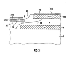
- FIG. 3 1 a semiconductor device is shown in which the first and the second contact regions 110 and 210 are arranged on the common layer surface 70 of the semiconductor device, but in contrast to the exemplary embodiment of FIG. 1 are spatially separated from each other.
- the function of the semiconductor device of FIG. 3 consists of controlling a current flow 50, which emanates from the first semiconductor region 100 or from the first contact region 110 and which passes through an n-SiC layer 2, within a channel region 8 of this n-SiC layer 2.
- the channel region 8 can be changed in its dimensions and thus in its resistance by the second semiconductor region 200 and a p-island 4 buried in the n-SiC layer 2. This is done by applying a voltage to the second contact region 210, whereby a depletion zone 20 at a Pn junction 19 between the n-type SiC layer 2 and the p-type second semiconductor region 200 among others in the channel region 8 into propagates.
- the dimension of the channel region 8 is additionally preset by providing a depression 30 in which the second semiconductor region 200 is located.
- Both the n-type first semiconductor region 100 and the p-type second semiconductor region 200 require an ohmic contact in the form of the first and second contact regions 110 and 210 for the described mode of operation.
- the first semiconductor region 100 has an n-doping with the donor phosphor, the second semiconductor region 200 a p-doping with the acceptor boron.
- the dopant concentration is in each case 10 19 cm -3 .
- a material for the first and the second contact region 110 and 210 is used in the example of FIG. 3 , which does not fall under the invention, a material mixture composed of the first material component tungsten and the second material component gallium.
- the volume fraction of gallium is about 5%.
- FIG. 4 shows a semiconductor device in the form of a vertical MOSFET based on silicon carbide.
- the MOSFET includes a plurality of first and second semiconductor regions 100 and 200.
- the in the Figures 1 and 2 shown semiconductor devices can be found in the MOSFET of FIG. 4 as substructures again. They are identified by a dashed circle or a dashed rectangle.
- the vertical MOSFET of FIG. 4 is mirror-symmetric with respect to a plane of symmetry 60.
- the lowest lying first semiconductor region 100 is also associated with FIG FIG. 4 as substrate 100a.
- the n - SiC layer 3 is arranged on one of which perpendicular to Symmetry plane 60 directed surface 40.
- the n - SiC layer 3 is arranged on one of which perpendicular to Symmetry plane 60 directed surface 40.
- the n - SiC layer 3 is arranged.
- 42 includes two separate, with respect to the plane of symmetry at a side facing away from the SiC substrate 100 a surface 60 arranged mirror-symmetrically p-layers 11, these include in turn each first and second semiconductor regions 100 and 200 which adjoin one another ,
- the first and second semiconductor regions 100 and 200 are electrically contacted by the first and second contact regions 110 and 210 associated therewith.
- the contiguous first and second contact regions 110 and 210 may be in the in FIG. 4 also be regarded as a source electrode 110a.
- a further first contact region 110 On one of the n - SiC layer 3 facing away from surface 41 of SiC substrate 100a, there is a further first contact region 110, which may be considered herein as a drain electrode 110b.
- the operation of the vertical MOSFETs of FIG. 4 to control the current flow 50 between the drain 110b and the source 110a runs through a vertical drift region 9 in the SiC substrate 100a and in the n - SiC layer 3, and a lateral channel region 80 in the p-layer 11.
- the resistance of the channel region 80 can be adjusted by a gate electrode 14 wherein an electrically insulating oxide layer 13 separates the gate electrode 14 from the channel region 80 in the p-layer 11.
- first and second semiconductor regions 100 and 200 with different conduction types is frequently required.
- the contacting takes place as in the examples of FIGS. 1 to 3 already described.
- semiconductor devices part of a complex semiconductor device, which consequently includes a plurality of first and second semiconductor regions 100 and 200 together with the contacting via the associated first and second contact regions 110 and 210.
Abstract
Description
- Die Erfindung bezieht sich auf eine Halbleiteranordnung mit ohmscher Kontaktierung sowie auf ein Verfahren zur Kontaktierung einer Halbleiteranordnung.
- Die Erfindung betrifft insbesondere eine derartige Halbleiteranordnung, die zumindest in bestimmten Halbleitergebieten, insbesondere den Halbleitergebieten, die kontaktiert werden, aus einem vorbestimmten Polytyp des Siliciumcarbids besteht.
- Siliciumcarbid (SiC) in einkristalliner Form ist ein Halbleitermaterial mit hervorragenden physikalischen Eigenschaften, die dieses Halbleitermaterial unter anderem aufgrund seiner hohen Durchbruchfeldstärke und seiner guten thermischen Leitfähigkeit besonders für die Leistungselektronik auch noch bei Anwendungen im kV-Bereich interessant erscheinen lassen. Da die kommerzielle Verfügbarkeit einkristalliner Substratwafer speziell aus Siliciumcarbid des 6H- und 4H-Polytyps gestiegen ist, finden nun auch Leistungshalbleiter Bauelemente auf Siliciumcarbidbasis wie z.B. Schottky-Dioden zunehmend an Beachtung. Andere Siliciumcarbid-Bauelemente mit steigendem Verbreitungsgrad sind pn-Dioden und Transistoren wie beispielsweise MOSFET's (Metal Oxide Semiconductor Field Effect Transistors).
- Für die Funktion dieser Bauelemente sind stabile ohmsche Kontakte zu Halbleitergebieten unterschiedlichen Leitungstyps unabdingbar. Dabei werden möglichst niedrige Kontaktwiderstände angestrebt, um unerwünschte Verluste am Übergang Halbleiter-Metall zu minimieren.
- In dem Übersichtsaufsatz "Ohmic contacts to SiC" von G.L: Harris et al. aus "Properties of Silicon Carbide" ed. by G.L. Harris INSPEC, 1995, Seiten 231-234 findet sich eine Zusammenstellung von Kontaktierungsverfahren für Siliciumcarbid verschiedenen Polytyps und Leitungstyps. Bezüglich der Kontaktierung von n- und p-leitendem SiC ist dem Übersichtsaufsatz sowie den zitierten Querreferenzen der in der Fachwelt derzeit allgemein anerkannte Kenntnisstand zu entnehmen, der im folgenden skizziert wird:
- Der genannte Übersichtsaufsatz gibt nur Verfahren an, bei denen Siliciumcarbid jeweils nur eines einzigen Leitungstyps mit einem ohmschen Kontakt versehen wird.
- Die Kontaktierung von n-leitendem SiC erfolgt demgemäß über eine dünne Kontaktschicht eines Metalls oder über Schichtfolge unterschiedlicher Materialien. Die Kontaktschichten werden bei Temperaturen zwischen 600°C und 1100°C getempert. Insbesondere Übergangsmetalle wie beispielsweise Nickel liefern nach der Temperaturbehandlung auf n-leitendem hochdotierten SiC einen sehr guten ohmschen Kontakt, da sich bei Temperaturen von um die 1000°C aus dem Übergangsmetall und dem im SiC enthaltenen Silicium ein Metallsilicid bildet. Kontakttechniken für n-leitendes SiC, die ohne eine entsprechende Temperaturbehandlung arbeiten, liefern im Vergleich dazu einen relativ hohen Kontaktwiderstand oder eine nicht dem ohmschen Gesetz entsprechende Strom-Spannungscharakteristik. Die Temperaturbehandlung wirkt sich darüber hinaus auch positiv auf die Temperaturstabilität der gebildeten ohmschen Kontakte aus.
- Zur Kontaktierung von p-leitendem SiC wird überwiegend Aluminium verwendet. Da Aluminium in SiC gut löslich ist und als Akzeptor wirkt, kann in einem Grenzbereich zwischen dem Aluminium enthaltenden Kontaktgebiet und dem Halbleitergebiet aus SiC eine mit Aluminium hochdotierte Zone erzeugt werden. Um ein Abdampfen des Aluminiums, das bereits bei 659°C schmilzt, bei einer nachfolgenden Temperaturbehandlung zu vermeiden, wird auf dem Aluminium mindestens eine Deckschicht aus einem Material mit einem höheren Schmelzpunkt wie z.B. Nickel, Wolfram, Titan oder Tantal aufgebracht.
- In dem Aufsatz " Thermally stable low ohmic contacts to p-type 6H-SiC using cobalt silicides" von N.Lundberg, M.Östling aus Solid-State Electronics, Vol. 39, No. 11, Seiten 1559-1565, 1996 wird ein Verfahren zur Kontaktierung von p-leitendem SiC offenbart, das sich der Bildung von Kobaltsilicid (CoSi2) bedient. Mit dem beschriebenen Verfahren und dem verwendeten Kontaktmaterial ist ein sehr niedriger Kontaktwiderstand zu erreichen.
- In dem Aufsatz " Reduction of Ohmic Contact Resistance on n-Type 6H-SiC by Heavy Doping" von T. Uemoto, Japanese Journal of Applied Physics, Vol. 34, 1995, Seiten L7 bis L9 wird ein Schichtaufbau aus einer 15 nm dicken Titan-Schicht und einer 150 nm dicken Aluminium-Schicht als möglicher ohmscher Kontakt sowohl auf p-leitendem als auch auf n-leitendem Siliciumcarbid offenbart. Ein guter Kontaktwiderstand auf dem n-leitenden Halbleitergebiet wird jedoch nur dann erzielt, wenn die Dotierstoffkonzentration in dem n-leitenden Halbleitergebiet sehr hoch gewählt wird. Die offenbarte Dotierstoffkonzentration von 4,5·1020 cm-3 liegt erheblich über den zur Zeit üblicherweise in einer Siliciumcarbid-Halbleiteranordnung verwendeten Dotierstoffkonzentrationen. Eine solch hohe Dotierstoffkonzentration läßt sich nur mit erheblichem Zusatzaufwand herstellen. So besteht z.B. beim Ionenimplantieren die Gefahr, daß das n-leitende Halbleitergebiet geschädigt wird.
- Die
WO 95/24055 A1 - Aus der
US-A-5 124 779 ist ein SiC-Halbleiterbauelement bekannt, dessen ohmscher Kontakt aus einer Titan-AluminiumLegierung besteht. Die als Kontaktelektrode dienende Legierung haftet dann besonders gut auf einer n- oder p-dotierten SiC-Schicht, wenn der Aluminiumanteil am Gesamtgewicht der Legierung im Bereich zwischen 15% und 65% liegt. - Aus L.M.Porter et al: "A critical review of ohmic and rectifying contacts for silicon carbide", Materials Science and Engineering B, Band 34 (1995) S. 83 - 105 ist bekannt, eine als Schottky-Kontakt dienende NiAl-Metallisierung mittels Elektronenstrahlverdampfung im Vakuum bei Zimmertemperatur auf p-dotiertem SiC abzuscheiden.
- Es ist Aufgabe der Erfindung, eine Halbleiteranordnung sowie ein Verfahren der eingangs bezeichneten Art mit einer im Vergleich zum Stand der Technik verbesserten Kontaktierung von n- und p-leitendem SiC anzugeben. Dabei sollen die Kontakte auf dem n- und p-leitenden Halbleitergebiet jeweils sowohl einen niedrigen Kontaktwiderstand haben als auch temperaturstabil sein. Außerdem sollen für das n- und p-leitende SiC nur Dotierstoffkonzentrationen vorgesehen werden, die sich mit derzeit verfügbaren Technologien einfach herstellen lassen.
- Zur Lösung der die Halbleiteranordnung betreffenden Teilaufgabe wird eine Halbleiteranordnung entsprechend den Merkmalen des unabhängigen Patentanspruches 1 angegeben.
- Zur Lösung der das Verfahren betreffenden Teilaufgabe wird ein Verfahren entsprechend den Merkmalen des unabhängigen Patentanspruchs 7 angegeben.
- Die Erfindung beruht dabei auf der Erkenntnis, daß entgegen der üblichen Vorgehensweise der Fachwelt, bei der n- und p-leitendes Siliciumcarbid mit jeweils unterschiedlichem Material ohmsch kontaktiert wird, eine Kontaktierung von Siliciumcarbid beiden Leitungstyps dennoch mit einem einzigen Material möglich ist. Daraus ergeben sich wesentliche Vorteile bei der Herstellung, da die für ein davon verschiedenes Kontaktmaterial benötigten Prozeßschritte entfallen.
- Für die Ausbildung eines guten ohmschen Kontakts ist es vorteilhaft, wenn das erste und zweite Halbleitergebiet jeweils eine ausreichend hohe Dotierstoffkonzentration zumindest an der Oberfläche des Halbleitergebietes aufweisen. Daher liegen die Dotierstoffkonzentrationen zwischen 10-17 cm-3 und 1020 cm-3 . Ein besonders guter Kontakt ergibt sich, wenn die Dotierstoffkonzentration mindestens 1019 cm-3 beträgt. Diese Angaben gelten sowohl für den n- als auch den p-Lei tungstyp. Diese Dotierstoffkonzentrationen lassen sich beispielsweise mittels Ionenimplantation problemlos erzeugen.
- Sie liegen insbesondere auch deutlich unter der im Stand der Technik genannten Dotierstoffkonzentration.
- Entscheidend für die Ausbildung eines guten ohmschen Kontaktwiderstands sowohl auf dem n-leitenden als auch p-leitenden Siliciumcarbid ist hierbei, daß das Material nicht in Form eines Schichtaufbaus, sondern vielmehr mit praktisch homogener Materialzusammensetzung auf die jeweiligen Halbleitergebiete aufgebracht wird. Bei Zusammensetzung des Materials aus mehreren Materialkomponenten wird durch einen solchen homogenen Materialauftrag erreicht, daß an der Grenzfläche zu den beiden Halbleitergebieten jeweils alle Materialkomponenten unmittelbar vorhanden sind und mit dem Siliciumcarbid der beiden Halbleitergebiete in Wechselwirkung treten können. Demgegenüber ist bei einem Schichtaufbau zunächst eine Durchmischung der in Form von Einzelschichten mit einer Dicke in der Größenordnung einiger Nanometer aufgetragenen einzelnen Materialkomponenten erforderlich. Diese Durchmischung (= Homogenisierung) findet dabei insbesondere zu Beginn eines nach dem Materialauftrag durchgeführten Temperprozesses statt. Ein solcher Temperprozeß hat aber in erster Linie auch die Formierung der ohmschen Kontakte zum Ziel. Es ist nun von entscheidendem Vorteil, wenn bei diesem Temperprozeß alle relevanten Materialkomponenten des Materials für die beiden Kontaktgebiete unmittelbar an der Grenzfläche zu den Halbleitergebieten vorhanden sind. Dadurch wird die Formierung der ohmschen Kontakte wesentlich begünstigt.
- Bei Aufbringen des gleichen Materials auf das erste und zweite Halbleitergebiet ist es gegebenenfalls je nach gewählter SiC-Dotierung und je nach für die beiden Kontaktgebiete verwendetem Material möglich, daß sich in einem ersten an das erste Halbleitergebiet angrenzenden Grenzbereich des ersten Kontaktgebiets und in einem zweiten an das zweite Halbleitergebiet angrenzenden Grenzbereich des zweiten Kontaktgebiets eine leicht voneinander abweichende Materialzusammensetzung einstellt. Diese geringfügige Abweichung rührt von unterschiedlichen Austauschvorgängen zwischen dem aufgebrachten Material und dem ersten oder dem zweiten Halbleitergebiet her.
- Enthält das aufgebrachte Material beispielsweise eine Materialkomponente, die in Siliciumcarbid als Donator oder Akzeptor wirkt, so wird diese Materialkomponente in gewissem Umfang in das erste oder zweite Halbleitergebiet wandern, wo sie beispielsweise als Dotierstoff an den entsprechenden Gitterstellen eingebunden wird. Dieser Durchmischungsvorgang wird maßgeblich durch die ursprüngliche Dotierung des ersten oder zweiten Halbleitergebiets beeinflußt und verläuft somit im ersten und zweiten Grenzbereich unterschiedlich. Dadurch verändert sich der Anteil der betreffenden Materialkomponente zumindest im ersten und zweiten Grenzbereich in voneinander abweichendem, wenn auch sehr geringem Umfang.
- Desgleichen ergibt sich eine Verschiebung der Materialzusammensetzung im Grenzbereich des ersten oder zweiten Kontaktgebiets, wenn das Material eine silicidbildende Materialkomponente enthält. In diesem Fall durchmischt sich Silicium, das aus dem ersten und zweiten Halbleitergebiet stammt, mit dem Material des ersten und zweiten Kontaktgebietes. Infolge bildet sich dann u.a. in den beiden Grenzbereichen ein Silicid auf Basis der Materialkomponente und des Siliciums. Auch bei diesem Prozeß sind Dotierungsgrad und Leitungstyp maßgebliche Einflußfaktoren, so daß dieser Effekt ebenfalls zu einer leicht voneinander abweichenden Materialzusammensetzung im ersten und zweiten Grenzbereich führen kann.
- In den von den Grenzflächen entfernter lokalisierten Bereichen der beiden Kontaktgebiete wirken sich die beschriebenen Grenzflächeneffekte nicht aus, so daß das Material in seiner ursprünglich aufgebrachten Zusammensetzung erhalten bleibt und sich somit in diesen Bereichen des ersten und zweiten Kontaktgebiets gleicht.
- Bei der erfingungsgemäßen Lehre werden alle geringfügigen Unterschiede in der Materialzusammensetzung des ersten und zweiten Kontaktgebiets wie die, die auf den beschriebenen oder ähnlichen Grenzflächeneffekten beruhen, nicht als maßgeblich betrachtet und unter den Begriffen "zumindest annähernd gleiche Materialzusammensetzung" und "praktisch homogen" subsumiert.
- Außerdem werden Unterschiede in der Materialzusammensetzung, die auf übliche, gegebenenfalls unterschiedliche Verunreinigungen in Ausgangssubstanzen zurückzuführen sind, hier ebenfalls als nicht maßgeblich betrachtet.
- Es ist darüber hinaus im Rahmen der erfindungsgemäßen Lehre möglich, auf das erste und zweite Halbleitergebiet leicht unterschiedliches Material aufzubringen. Solange die Materialzusammensetzungen jedoch um weniger als 10% voneinander abweichen, werden sie hier ebenfalls als "zumindest annähernd gleich" bezeichnet.
- Besondere Ausgestaltungen und Weiterbildungen der Halbleiteranordnung und des Verfahrens nach der Erfindung ergeben sich aus den jeweils abhängigen Unteransprüchen.
- Das aufgebrachte Material setzt sich aus einer ersten und zweiten Materialkomponente zusammen. Die erste Materialkomponente besteht aus aus einem Werkstoff, der einen ohmschen Kontakt auf n-leitendem Siliciumcarbid bildet mit einem Kontaktwiderstand ≤ 10-1 Ωcm2, vorzugsweise ≤ 10-3 Ωcm2 Die zweite Materialkomponente enthält dagegen ein Element der dritten Hauptgruppe des Periodensystems. Durch die erste Materialkomponente wird ein stabiler ohmscher Kontakt auf demjenigen Halbleitergebiet, das n-leitend ist, erzeugt, durch die zweite Materialkomponente entsteht dagegen ein stabiler ohmscher Kontakt auf dem p-leitenden Halbleitergebiet.
- Die zweite Materialkomponente liegt mit einem Volumen-Anteil von 0,1 bis 50% in dem Material vor. Bevorzugt ist dabei ein Anteil von 0,5 bis 20%.
- Erfindungsgemäß ist Die erste Materialkomponente Nickel und die zweite Materialkomponente Aluminium, d.h. das Material besteht ausschließlich aus Nickel und Aluminium Es zeichnet sich aufgrund des Nickels durch einen guten ohmschen Kontakt auf dem n-leitenden Halbleitergebiet aus.
- Die Beimengung von Aluminium zum Nickel in dem oben angegebenen Konzentrationsbereich beeinträchtigt den Kontaktwiderstand auf dem n-leitenden Halbleitergebiet nicht oder nur geringfügig. Außerdem verhindert der Nickel-Anteil im Material auch die Bildung von flüssigen Aluminium-Inseln und das resultierende unerwünschte Abdampfen von Aluminium bei dem Temperprozeß, der zur Formierung des ohmschen Kontakts vorteilhafterweise durchgeführt wird.
- Vorteilhafte Ausführungsformen des Verfahrens, die sich aus den entsprechenden Unteransprüchen ergeben, weisen im wesentlichen die gleichen Vorteile auf wie die obengenannten jeweils korrespondierenden Weiterbildungen der Halbleiteranordnung selbst.
- Andere Ausbildungen des Verfahrens beziehen sich auf das Aufbringen des Materials auf das erste und zweite Halbleitergebiet.
- Besonders vorteilhaft ist eine Ausbildung, bei der das erste und zweite Kontaktgebiet gleichzeitig hergestellt werden. Dadurch reduziert sich die Anzahl der im Vergleich zu einem, sukzessiven Aufbringen benötigten Prozeßschritte erheblich. Somit können kürzere Fertigungszyklen erreicht werden.
- In einer weiteren Ausbildung des Verfahrens wird das Material, das auf die beiden Halbleitergebiete aufgebracht wird, zwei getrennten Quellen entnommen. Die Quellen enthalten dabei jeweils eine Materialkomponente, d.h. die erste oder die zweite. Die Entnahme erfolgt durch gleichzeitiges Verdampfen oder Zerstäuben (Sputtern). Die beiden Kontaktgebiete werden anschließend durch Abscheiden der Materialkomponenten auf dem ersten und zweiten Halbleitergebiet gebildet. Das Material für die beiden Kontaktgebiete entsteht dabei entweder noch in der Gasphase aus den einzelnen Materialkomponenten, im Laufe des Abscheidevorgangs oder erst danach. Durch die Prozeßparameter kann gewährleistet werden, daß ein bestimmtes beabsichtigtes Mischungsverhältnis eingehalten wird.
- Eine alternative Ausbildung sieht dagegen vor, daß aus der ersten und zweiten Materialkomponente zunächst ein Quellmaterial hergestellt wird, das dann in einem zweiten Verfahrensschritt zerstäubt wird. Die herausgelösten Partikel des Materials bilden wie in der vorher beschriebenen Ausbildung die beiden Kontaktgebiete auf dem n- und p-leitenden Siliciumcarbid.
- Bei einer anderen Ausbildung des Verfahrens werden die erste und die zweite Materialkomponente abwechselnd in dünnen Schichten auf die beiden Halbleitergebiete aufgetragen. Dies kann durch Sputtern aus zwei getrennten Quellen erfolgen, so daß abwechselnd in kurzer zeitlicher Abfolge jeweils nur eine der beiden Materialkomponenten aus der zugehörigen Quelle zerstäubt und als dünne Schicht auf den beiden Halbleitergebieten abgeschieden wird. Die resultierenden dünnen Schichten haben insbesondere nur eine Dicke in der Größenordnung einiger Ängström. Im Extremfall kann eine solche dünne Schicht auch nur aus einer einzigen Atomschicht, einer sog. Monolage, bestehen. Aufgrund der geringen Schichtdicke und der kurzen zeitlichen Abfolge bei der Schichtabscheidung wird auch dieser Materialauftrag der beiden Materialkomponenten hier noch als gleichzeitig bezeichnet. Eine Durchmischung der Atome dieser Monolagen (Homogenisierung) findet dann abhängig von den Prozeßbedingungen zumindest teilweise bereits während des Auftragens selbst oder gleich zu Beginn des sich anschließenden Temperprozesses statt. Aufgrund der geringen Schichtdicken dauert dieser Durchmischungsvorgang nur sehr kurze Zeit.
- In einer vorteilhaften Ausführungsvariante wird die Halbleiteranordnung, nachdem die beiden Kontaktgebiete aufgebracht worden sind, einem kurzzeitigen Temperprozeß unterzogen. Bevorzugt wird die Halbleiteranordnung dabei auf eine Maximaltemperatur von mindestens 500°C, insbesondere von etwa 1000°C, erhitzt und dann für bis zu 2 Stunden, insbesondere für 2 Minuten, auf etwa dieser Maximaltemperatur gehalten. Der Temperprozeß kann aber auch nur aus einer Aufheizphase und einer unmittelbar folgenden Abkühlphase bestehen, ohne daß dazwischen eine Verweildauer bei einer Maximaltemperatur vorgesehen wird. Dieser Prozeß dient der Formierung der beiden Kontaktgebiete. Es zeigt sich, daß nach diesem Temperprozeß sowohl auf dem ersten als auch auf dem zweiten Halbleitergebiet, also auf n- und p-leitendem SiC, temperaturstabile Kontakte mit guter ohmscher Charakteristik und niedrigem Kontaktwiderstand resultieren.
- In weiteren Ausführungsformen der Halbleiteranordnung sind das erste und zweite Kontaktgebiet auf einer gemeinsamen Schichtoberfläche oder auf verschiedenen Schichtoberflächen angeordnet. Für beide Ausführungsformen gelten die oben beschriebenen Weiterbildungsmöglichkeiten und Vorteile der Kontaktierung von n- und p-leitendem SiC mit dem gleichen Material in analoger Weise.
- Des weiteren sind Ausführungsvarianten möglich, in denen die beiden Kontaktgebiete zusammenhängend oder auch getrennt ausgebildet sind. Dabei kann die Trennung der beiden Kontaktgebiete sowohl bereits während des Aufbringens des Materials durch entsprechende Maskentechnik als auch danach durch Abtragen von zuviel aufgebrachtem Material erfolgen. Für letzteres kommen gängige Technologien wie z.B. das Ätzen in Frage.
- Die zu kontaktierenden beiden Halbleitergebiete können aus SiC verschiedenen Polytyps bestehen. Es gibt Ausführungsformen, bei denen SiC in Form von 6H-, 4H-, 15R- oder 3C-SiC für die beiden Halbleitergebiete verwendet wird. Andere Polytypen sind jedoch ebenfalls möglich.
- Außerhalb des ersten und zweiten Halbleitergebiets kann die Halbleiteranordnung auch aus einem anderen Material als SiC bestehen. Deshalb ist in einer Ausführungsform zumindest ein weiteres Halbleitergebiet, beispielsweise ein Substrat, aus einem von SiC verschiedenen Material, beispielsweise aus Silicium (Si), Galliumarsenid (GaAs) oder Galliumnitrid (GaN), vorgesehen. Dieses Substrat ist dann zumindest mit dem ersten und zweiten Halbleitergebiet aus SiC zu einer hybriden Halbleiteranordnung integriert.
- In einer Ausführungsform der Halbleiteranordnung befindet sich das erste und zweite Kontaktgebiet jeweils an einer frei zugänglichen Oberfläche der Halbleiteranordnung. Dies ist jedoch nicht zwingend notwendig. In anderen Weiterbildungen können das erste und zweite Kontaktgebiet auch durch Schichten, die in der Kontaktierung folgenden Prozeßschritten aufgebracht werden, bedeckt sein.
- Ausführungsbeispiele gemäß der Erfindung werden nunmehr anhand der Zeichnung näher erläutert. Zur Verdeutlichung ist die Zeichnung nicht maßstäblich ausgeführt und gewisse Merkmale sind schematisiert dargestellt. Im einzelnen zeigen:
- Figur 1
- eine Halbleiteranordnung mit zwei zusammenhängenden Kontaktgebieten,
- Figur 2
- eine Halbleiteranordnung mit zwei getrennten Kon- taktgebieten,
- Figur 3
- eine nicht -erfindungsgemäße Halbleiteranordnung mit zwei getrennten Kontaktgebieten und
- Figur 4
- eine Halbleiteranordnung in Form eines vertikalen MOSFET's unter Verwendung der Halbleiteranordnungen von
Figur 1 und 2 . - Einander entsprechende Teile sind in den
Figuren 1 bis 4 mit denselben Bezugszeichen versehen. - In
Figur 1 ist eine Halbleiteranordnung dargestellt, bei der sich ein erstes Kontaktgebiet 110 und ein zweites Kontaktgebiet 210 als zusammenhängende Schicht über ein erstes Halbleitergebiet 100 und ein diesem benachbartes zweites Halbleitergebiet 200 erstrecken. Das erste und zweite Halbleitergebiet 100 und 200 bestehen jeweils aus 6H-Siliciumcarbid. Sie besitzen eine gemeinsame Schichtoberfläche 70, auf der das erste und zweite Kontaktgebiet 110 und 210 angeordnet sind. - Das erste Halbleitergebiet 100 ist mit einem hohen Anteil an Donatoren, im vorliegenden Fall mit Stickstoff, dotiert und somit n-leitend. Das zweite Halbleitergebiet 200 weist dagegen eine hohe Dotierstoffkonzentration an Aluminium auf. Aluminium stellt in Siliciumcarbid einen Akzeptor dar, so daß das zweite Halbleitergebiet folglich p-leitend ist. Die Donatoren und Akzeptoren werden mittels Ionenimplantation in das erste bzw. zweite Halbleitergebiet 100 bzw. 200 eingebracht. Die Dotierstoffkonzentrationen im ersten und zweiten Halbleitergebiet 100 und 200 liegen bei jeweils 1013 cm-3. Diese hohen Dotierstoffkonzentrationen werden in der
Figur 1 durch die Symbole n+ und p- angezeigt. - Zur temperaturstabilen ohmschen Kontaktierung befinden sich auf dem ersten und zweiten Halbleitergebiet 100 und 200 das erste und zweite Kontaktgebiet 110 und 210. Die beiden Kontaktgebiete 110 und 210 bestehen aus dem gleichen Material, das sich aus einer ersten und einer zweiten Materialkomponente zusammensetzt. Die erste Materialkomponente ist Nickel, die zweite Aluminium. Für Aluminium liegt der Volumen-Anteil bei etwa 10%.
- Das Material für das erste und das zweite Kontaktgebiet 110 und 210 wird durch Verdampfen aus nicht dargestellten, getrennten Nickel- bzw. Aluminium-Quellen erzeugt. Anschließend erfolgt die Bildung des ersten und zweiten Kontaktgebiets 110 und 210 durch Abscheiden des gasförmigen Materials auf dem ersten und zweiten Halbleitergebiet 100 und 200. Zur Formierung und zur Bildung ohmscher, temperaturstabiler Kontakte wird die Halbleiteranordnung von
Figur 1 anschlieβend einem ca. zweiminütigem Temperprozeß bei etwa 1000°C unterzogen. Danach ergibt sich zwischen dem ersten Halbleitergebiet 100 (n-leitend) und dem ersten Kontaktgebiet 110 ein Kontaktwiderstand von unter 10-4 Ωcm2 und zwischen dem zweiten Halbleitergebiet 200 (p-leitend) und dem zweiten Kontaktgebiet 210 ein Kontaktwiderstand von unter 10-3 Ωcm2. - In
Figur 1 sind Grenzbereiche des ersten und zweiten Kontaktgebiets 110 und 210 mit den Bezugszeichen 120 bzw. 220 gekennzeichnet. Innerhalb dieser Grenzbereiche 120 und 220 ergeben sich aufgrund von Austauschvorgängen zwischen dem ersten Halbleitergebiet 100 und dem ersten Kontaktgebiet 110 sowie dem zweiten Halbleitergebiet 200 und dem zweiten Kontaktgebiet 210 geringfügige Veränderungen in der Zusammensetzung des ursprünglich im ersten und zweiten Kontaktgebiet 110 und 210 aufgebrachten Materials. Abgesehen von den resultierenden geringfügigen Unterschieden in der Materialzusammensetzung des ersten und des zweiten Grenzbereichs 120 und 220 weisen das erste und das zweite Kontaktgebiet 110 und 210 die gleiche Materialzusammensetzung auf. Es ist ebenfalls möglich, daß sich die Grenzbereiche 120 und 220, in denen die genannten Austauschvorgänge stattfinden, auch bis in die Halbleitergebiete 100 bzw. 200 erstrecken. InFigur 1 ist dieser Fall allerdings nicht dargestellt. -
Figur 2 zeigt eine Halbleiteranordnung in einer Schichtfolge mit dem ersten Kontaktgebiet 110 als unterster Schicht, dem zweiten Kontaktgebiet 210 als oberster Schicht sowie mehreren dazwischenliegenden SiC-Schichten. Das erste und zweite Kontaktgebiet 110 und 210 weisen wiederum den an die jeweilige benachbarte SiC-Schicht angrenzenden ersten bzw. zweiten Grenzbereich 120 und 220 auf. Der Teilstapel aus den SiC-Schichten setzt sich in aufsteigender Reihenfolge aus dem ersten Halbleitergebiet 100, einer n--SiC-Schicht 3, einer p-SiC-Schicht 11 sowie dem zweiten Halbleitergebiet 200 zusammen. Das erste Kontaktgebiet 110 ist dabei auf einer ersten Schichtoberflächen 71 des ersten Halbleitergebiets 100, die zugleich auch eine untere Hauptoberfläche des Teilstapels aus den SiC-Schichten bildet, angeordnet. Das zweite Kontaktgebiet 210 ist auf einer zweiten Schichtoberflächen 72 des zweiten Halbleitergebiets 200, die zugleich eine obere Hauptoberfläche des Teilstapels aus den SiC-Schichten bildet, angeordnet. - Das erste Halbleitergebiet 100, das im Ausführungsbeispiel von
Figur 2 auch ein SiC-Substrat 100a darstellen kann, besitzt wieder eine hohe n-Leitfähigkeit, das zweite Halbleitergebiet 200 dagegen eine hohe p-Leitfähigkeit. Die im ersten und zweiten Halbleitergebiet 100 und 200 sowie im ersten und zweiten Kontaktgebiet 110 und 210 vorgesehenen Materialien und Dotierstoffe entsprechen denen des Ausführungsbeispiels vonFigur 1 . Diese Analogie gilt auch für das Verfahren zum Aufbringen des ersten und zweiten Kontaktgebiets 110 und 210. - Die Halbleiteranordnung von
Figur 2 besitzt zwischen der n--SiC-Schicht 3 und der p-Schicht 11 einen pn-Übergang 17, der die Funktion dieser Halbleiteranordnung wesentlich bestimmt. Ein derartiger pn-Übergang 17 kann sowohl Bestandteil einer größeren Schaltungsanordnung sein, als auch ein eigenes Bauelement in Form einer pn-Diode darstellen. In beiden Fällen ist eine ohmsche Kontaktierung von Halbleitergebieten unterschiedlichen Leitungstyps über die Kontaktgebiete 110 und 210 notwendig. - Die in
Figur 2 gezeigte Ausführungsform ist ein Beispiel für eine Halbleiteranordnung mit erstem und zweiten Kontaktgebiet 110 und 210 auf verschiedenen Schichtoberflächen 71 und 72 der Halbleiteranordnung. - In
Figur 3 ist eine Halbleiteranordnung dargestellt, bei der das erste und das zweite Kontaktgebiet 110 und 210 auf der gemeinsamen Schichtoberfläche 70 der Halbleiteranordnung angeordnet sind, jedoch im Unterschied zu dem Ausführungsbeispiel vonFigur 1 räumlich getrennt voneinander sind. - Die Funktion der Halbleiteranordnung von
Figur 3 besteht darin, einen Stromfluß 50, der vom ersten Halbleitergebiet 100 bzw. vom ersten Kontaktgebiet 110 ausgeht und der durch eine n-SiC-Schicht 2 verläuft, innerhalb eines Kanalbereichs 8 dieser n-SiC-Schicht 2 zu steuern. Dazu kann der Kanalbereich 8 durch das zweite Halbleitergebiet 200 und eine in der n-SiC-Schicht 2 vergrabene p-Insel 4 in seinen Dimensionen und damit seinem Widerstand verändert werden. Dies geschieht über das Anlegen einer Spannung an das zweite Kontaktgebiet 210, wodurch sich eine Verarmungszone 20 an einem pn-Übergang 19 zwischen der n-SiC-Schicht 2 und dem p-leitenden zweiten Halbleitergebiet 200 u.a. in den Kanalbereich 8 hinein ausbreitet. Die Dimension des Kanalbereichs 8 wird zusätzlich voreingestellt, indem eine Vertiefung 30 vorgesehen ist, in der sich das zweite Halbleitergebiet 200 befindet. - Sowohl das n-leitende erste Halbleitergebiet 100 als auch das p-leitende zweite Halbleitergebiet 200 benötigen für die beschriebene Funktionsweise eine ohmsche Kontaktierung in Form des ersten und zweiten Kontaktgebiets 110 und 210.
- Das erste Halbleitergebiet 100 weist eine n-Dotierung mit dem Donator Phosphor auf, das zweite Halbleitergebiet 200 eine p-Dotierung mit dem Akzeptor Bor. Die Dotierstoffkonzentration beträgt jeweils 1019 cm-3. Als Material für das erste und das zweite Kontaktgebiet 110 und 210 dient im Beispiel von
Figur 3 , das nicht unter die Erfindung fällt, ein Materialgemisch, das sich aus der ersten Materialkomponente Wolfram und der zweiten Materialkomponente Gallium zusammensetzt. Der Volumen-Anteil von Gallium beträgt hierbei etwa 5%. Das Aufbringen des Materialgemischs sowie der anschließende Temperprozeß erfolgen wie im Zusammenhang mitFigur 1 und 2 bereits beschrieben. - Die
Figur 4 zeigt eine Halbleiteranordnung in Form eines vertikalen MOSFET's auf Basis von Siliciumcarbid. Der MOSFET beinhaltet dabei mehrere erste und zweite Halbleitergebiete 100 und 200. Die in denFiguren 1 und 2 gezeigten Halbleiteranordnungen finden sich in dem MOSFET vonFigur 4 als Teilstrukturen wieder. Sie sind durch einen gestrichelten Kreis bzw. ein gestricheltes Rechteck kenntlich gemacht. - Der vertikale MOSFET von
Figur 4 ist spiegelsymmetrisch bezüglich einer Symmetrieebene 60. Analog zuFigur 2 wird das in der dargestellten Schichtfolge zuunterst liegende erste Halbleitergebiet 100 auch im Zusammenhang mitFigur 4 als Substrat 100a bezeichnet. Auf dessen einer senkrecht zur Symmetrieebene 60 gerichteten Oberfläche 40 ist die n--SiC-Schicht 3 angeordnet. Innerhalb dieser n--SiC-Schicht 3 befinden sich an einer vom SiC-Substrat 100a abgewandten Oberfläche 42 zwei separate, bezüglich der Symmetrieebene 60 spiegelsymmetrisch angeordnete p-Schichten 11. Diese beinhalten ihrerseits jeweils ein erstes und zweites Halbleitergebiet 100 und 200, die aneinandergrenzen. Das erste und zweite Halbleitergebiet 100 und 200 sind durch die hier zusammenhängenden ersten und zweiten Kontaktgebiete 110 und 210 elektrisch kontaktiert. Die zusammenhängenden ersten und zweiten Kontaktgebiete 110 und 210 können in dem inFigur 4 dargestellten Ausführungsbeispiel auch als eine Source-Elektrode 110a angesehen werden. Auf einer von der n--SiC-Schicht 3 abgewandten Oberfläche 41 des SiC-Substrats 100a befindet sich ein weiteres erstes Kontaktgebiet 110, das hier auch als eine Drain-Elektrode 110b angesehen werden kann. - Ähnlich dem in
Figur 3 beschriebenen Ausführungsbeispiel besteht die Funktionsweise des vertikalen MOSFET's vonFigur 4 darin, den Stromfluß 50 zwischen der Drain-Elektrode 110b und der Source-Elektrode 110a zu steuern. Der Stromfluß 50 durchläuft dabei einen vertikalen Driftbereich 9 im SiC-Substrat 100a und in der n--SiC-Schicht 3 sowie einen lateralen Kanalbereich 80 in der p-Schicht 11. Der Widerstand des Kanalbereichs 80 kann über eine Gate-Elektrode 14 eingestellt werden, wobei eine elektrisch isolierende Oxidschicht 13 die Gate-Elektrode 14 vom Kanalbereich 80 in der p-Schicht 11 trennt. - Wie das Ausführungsbeispiel des MOSFET's demonstriert, wird gerade auch in komplexeren Halbleiteranordnungen häufig eine elektrische Kontaktierung von ersten und zweiten Halbleitergebieten 100 und 200 mit verschiedenem Leitungstyp benötigt. Die Kontaktierung erfolgt dabei wie in den Beispielen der
Figuren 1 bis 3 bereits beschrieben. In einer nicht dargestellten Ausführungsform sind mehrere der in denFiguren 1 bis 4 gezeigten Halbleiteranordnungen Bestandteil einer komplexen Halbleiteranordnung, die folglich eine Vielzahl von ersten und zweiten Halbleitergebieten 100 und 200 nebst der Kontaktierung über die zugehörigen ersten und zweiten Kontaktgebiete 110 und 210 beinhaltet.
Claims (13)
- Halbleiteranordnung mit ohmscher Kontaktierung, wobei die Halbleiteranordnung aufweist:a) mindestens ein aus n-leitendem Siliciumcarbid bestehendes erstes Halbleitergebiet (100),b) mindestens ein aus p-leitendem Siliciumcarbid bestehendes zweites Halbleitergebiet (200), wobei die Dotierstoffkonzentrationen des n-leitenden Siliciumcarbids und des p-leitenden Siliciumcarbids jeweils im Bereich zwischen 1017 cm-3 und 1020 cm-3 liegen,c) mindestens ein an das erste Halbleitergebiet (100) anangrenzendes erstes Kontaktgebiet (110) undd) mindestens ein an das zweite Halbleitergebiet (200) angrenzendes zweites Kontaktgebiet (210),e) wobei das erste und das zweite Kontaktgebiet (110, 210) das erste und das zweite Halbleitergebiet jeweils ohmsch kontaktieren und aus dem gleichen, praktisch homogenen und ausschließlich Nickel und Aluminium enthaltenden Material bestehen, wobei der Volumenanteil des Aluminiums im Bereich zwischen 0,1% und 50% liegt.
- Halbleiteranordnung nach Anspruch 1, dadurch
gekennzeichnet, daß das erste und das zweite Kontaktgebiet (110, 210) auf einer gemeinsamen Schichtoberfläche (70) angeordnet sind. - Halbleiteranordnung nach Anspruch 1, dadurch gekennzeichnet, daß das erste und das zweite Kontaktgebiet (110, 210) auf verschiedenen Schichtoberflächen (71, 72) angeordnet sind.
- Halbleiteranordnung nach Anspruch 1 oder 2, dadurch gekennzeichnet, daß das erste und das zweite Kontaktgebiet (110, 210) zusammenhängend ausgebildet sind.
- Halbleiteranordnung nach einem der Ansprüche 1 bis 3,
dadurch gekennzeichnet, daß das erste und das zweite Kontaktgebiet (110, 210) getrennt ausgebildet sind. - Halbleiteranordnung nach einem der Ansprüche 1 bis 5,
dadurch gekennzeichnet, daß der Volumenanteil des Aluminiums im Bereich zwischen 0,5% und 20% liegt. - Verfahren zur ohmschen Kontaktierung einer Halbleiteranordnung, bei dem
ein erstes Kontaktgebiet (110) auf einem aus n-leitendem Siliciumcarbid bestehenden, eine im Bereich zwischen 1017 cm-3 und 1020 cm-3 liegende Dotierstoffkonzentration aufweisenden ersten Halbleitergebiet (100) und ein zweites Kontaktgebiet (210) auf einem aus p-leitendem, Siliciumcarbid bestehenden, eine im Bereich zwischen 1017 cm-3 und 1020 cm-3 liegende Dotierstoffkonzentration aufweisenden zweiten Halbleitergebiet (200) durch Aufbringen des gleichen, praktisch homogenen und ausschließlich Nickel und Aluminium enthaltenden Materials derart erzeugt werden, dass der Volumenanteil des Aluminiums in dem Material zwischen 0,1% und 50% liegt. - Verfahren nach Anspruch 7, dadurch gekennzeichnet, daß das erste und das zweite Kontaktgebiet (110, 210) gleichzeitig auf das erste und zweite Halbleitergebiet (100, 200) aufgebracht werden.
- Verfahren nach Anspruch 7 oder 8, dadurch gekennzeichnet, dass der Volumenanteil des Aluminiums in dem aufgebrachten Material im Bereich zwischen 0,5% und 20% liegt.
- Verfahren nach einem der Ansprüche 7 bis 9, dadurch gekennzeichnet, daß das Material durch gleichzeitiges Verdampfen oder Zerstäuben aus einer Nickelquelle und einer Aluminiumquelle aufgebracht wird.
- Verfahren nach einem der Ansprüche 7 bis 9, dadurch gekennzeichnet, daß eine Nickel und Aluminium enthaltende Quelle vorab hergestellt wird und das Material dann durch Zerstäuben des Quellenmaterials aufgebracht wird.
- Verfahren nach einem oder Ansprüche 7 bis 11, dadurch gekennzeichnet, daß die das erste und zweite Halbleitergebiet (100, 200) sowie das aufgebrachte erste und zweite Kontaktgebiet (110, 210) umfassende Halbleiteranordnung einem Temperprozeß mit einer Erhitzung auf eine Maximaltemperatur von mindestens 500°C, vorzugsweise von etwa 1000°C, unterzogen wird.
- Verfahren nach Anspruch 12, dadurch gekennzeichnet, daß die Maximaltemperatur für eine Dauer von höchstens 2 Minuten bis höchstens 2 Stunden konstant gehalten wird.
Applications Claiming Priority (3)
| Application Number | Priority Date | Filing Date | Title |
|---|---|---|---|
| DE19825519 | 1998-06-08 | ||
| DE19825519 | 1998-06-08 | ||
| PCT/DE1999/001659 WO1999065067A1 (de) | 1998-06-08 | 1999-06-07 | Halbleiteranordnung mit ohmscher kontaktierung und verfahren zur kontaktierung einer halbleiteranordnung |
Publications (2)
| Publication Number | Publication Date |
|---|---|
| EP1090415A1 EP1090415A1 (de) | 2001-04-11 |
| EP1090415B1 true EP1090415B1 (de) | 2010-11-17 |
Family
ID=7870259
Family Applications (1)
| Application Number | Title | Priority Date | Filing Date |
|---|---|---|---|
| EP99938136A Expired - Lifetime EP1090415B1 (de) | 1998-06-08 | 1999-06-07 | Halbleiteranordnung mit ohmscher kontaktierung und verfahren zur kontaktierung einer halbleiteranordnung |
Country Status (4)
| Country | Link |
|---|---|
| US (1) | US6667495B2 (de) |
| EP (1) | EP1090415B1 (de) |
| DE (2) | DE19925233A1 (de) |
| WO (1) | WO1999065067A1 (de) |
Families Citing this family (11)
| Publication number | Priority date | Publication date | Assignee | Title |
|---|---|---|---|---|
| US20040120371A1 (en) * | 2000-02-18 | 2004-06-24 | Jds Uniphase Corporation | Contact structure for a semiconductor component |
| DE10036208B4 (de) * | 2000-07-25 | 2007-04-19 | Siced Electronics Development Gmbh & Co. Kg | Halbleiteraufbau mit vergrabenem Inselgebiet und Konaktgebiet |
| DE10051049B4 (de) * | 2000-10-14 | 2011-04-07 | Cree, Inc. | Aluminium-Nickel-Kontaktmetallisierung für p-dotiertes SiC und Herstellungsverfahren dafür |
| JP2003173673A (ja) * | 2001-11-30 | 2003-06-20 | Sanyo Electric Co Ltd | 強誘電体メモリ |
| US7138291B2 (en) * | 2003-01-30 | 2006-11-21 | Cree, Inc. | Methods of treating a silicon carbide substrate for improved epitaxial deposition and resulting structures and devices |
| JP4122880B2 (ja) * | 2002-07-24 | 2008-07-23 | 住友電気工業株式会社 | 縦型接合型電界効果トランジスタ |
| CA2576960A1 (en) * | 2004-07-08 | 2007-01-04 | Semisouth Laboratories, Inc. | Monolithic vertical junction field effect transistor and schottky barrier diode fabricated from silicon carbide and method for fabricating the same |
| US8026160B2 (en) * | 2005-09-08 | 2011-09-27 | Mitsubishi Electric Corporation | Semiconductor device and semiconductor device manufacturing method |
| CN101578705B (zh) * | 2007-07-20 | 2012-05-30 | 松下电器产业株式会社 | 碳化硅半导体装置及其制造方法 |
| JP4858791B2 (ja) * | 2009-05-22 | 2012-01-18 | 住友電気工業株式会社 | 半導体装置およびその製造方法 |
| US9466698B2 (en) * | 2013-03-15 | 2016-10-11 | Semiconductor Components Industries, Llc | Electronic device including vertical conductive regions and a process of forming the same |
Family Cites Families (17)
| Publication number | Priority date | Publication date | Assignee | Title |
|---|---|---|---|---|
| US3662458A (en) * | 1969-06-20 | 1972-05-16 | Westinghouse Electric Corp | Electrical contact for silicon carbide members |
| US3982262A (en) * | 1974-04-17 | 1976-09-21 | Karatsjuba Anatoly Prokofievic | Semiconductor indicating instrument |
| US4320251A (en) * | 1980-07-28 | 1982-03-16 | Solamat Inc. | Ohmic contacts for solar cells by arc plasma spraying |
| US4918497A (en) * | 1988-12-14 | 1990-04-17 | Cree Research, Inc. | Blue light emitting diode formed in silicon carbide |
| US5027168A (en) * | 1988-12-14 | 1991-06-25 | Cree Research, Inc. | Blue light emitting diode formed in silicon carbide |
| JP2509713B2 (ja) * | 1989-10-18 | 1996-06-26 | シャープ株式会社 | 炭化珪素半導体装置およびその製造方法 |
| US5281831A (en) * | 1990-10-31 | 1994-01-25 | Kabushiki Kaisha Toshiba | Optical semiconductor device |
| US5264713A (en) * | 1991-06-14 | 1993-11-23 | Cree Research, Inc. | Junction field-effect transistor formed in silicon carbide |
| US5465249A (en) * | 1991-11-26 | 1995-11-07 | Cree Research, Inc. | Nonvolatile random access memory device having transistor and capacitor made in silicon carbide substrate |
| US5539217A (en) * | 1993-08-09 | 1996-07-23 | Cree Research, Inc. | Silicon carbide thyristor |
| DE59504562D1 (de) * | 1994-03-04 | 1999-01-28 | Siemens Ag | Mis-struktur auf siliciumcarbid-basis mit hoher latch-up-festigkeit |
| US5449925A (en) * | 1994-05-04 | 1995-09-12 | North Carolina State University | Voltage breakdown resistant monocrystalline silicon carbide semiconductor devices |
| US5523589A (en) * | 1994-09-20 | 1996-06-04 | Cree Research, Inc. | Vertical geometry light emitting diode with group III nitride active layer and extended lifetime |
| JPH0897441A (ja) * | 1994-09-26 | 1996-04-12 | Fuji Electric Co Ltd | 炭化けい素ショットキーダイオードの製造方法 |
| US5929523A (en) * | 1996-03-07 | 1999-07-27 | 3C Semiconductor Corporation | Os rectifying Schottky and ohmic junction and W/WC/TiC ohmic contacts on SiC |
| US6180958B1 (en) * | 1997-02-07 | 2001-01-30 | James Albert Cooper, Jr. | Structure for increasing the maximum voltage of silicon carbide power transistors |
| US6011278A (en) * | 1997-10-28 | 2000-01-04 | Philips Electronics North America Corporation | Lateral silicon carbide semiconductor device having a drift region with a varying doping level |
-
1999
- 1999-06-01 DE DE19925233A patent/DE19925233A1/de not_active Withdrawn
- 1999-06-07 EP EP99938136A patent/EP1090415B1/de not_active Expired - Lifetime
- 1999-06-07 DE DE59915222T patent/DE59915222D1/de not_active Expired - Lifetime
- 1999-06-07 WO PCT/DE1999/001659 patent/WO1999065067A1/de active Application Filing
-
2000
- 2000-12-08 US US09/732,989 patent/US6667495B2/en not_active Expired - Lifetime
Also Published As
| Publication number | Publication date |
|---|---|
| WO1999065067A1 (de) | 1999-12-16 |
| US20010001484A1 (en) | 2001-05-24 |
| DE19925233A1 (de) | 1999-12-09 |
| DE59915222D1 (de) | 2010-12-30 |
| US6667495B2 (en) | 2003-12-23 |
| EP1090415A1 (de) | 2001-04-11 |
Similar Documents
| Publication | Publication Date | Title |
|---|---|---|
| DE112015004093B4 (de) | Siliciumcarbid-halbleitervorrichtung und verfahren zum herstellen einer siliciumcarbid-halbleitervorrichtung | |
| EP1222694B1 (de) | SiC-Halbleitervorrichtung mit einem Schottky-Kontakt und Verfahren zu deren Herstellung | |
| DE60031173T2 (de) | Misfet | |
| DE3141967C2 (de) | ||
| DE102015103070B4 (de) | Leistungshalbleitervorrichtung mit trenchgatestrukturen mit zu einer hauptkristallrichtung geneigten längsachsen und herstellungsverfahren | |
| DE112018003362T5 (de) | Oxid-halbleitereinheit und verfahren zur herstellung einer oxid-halbleitereinheit | |
| DE102009033302B4 (de) | Herstellungsverfahren für ein unipolares Halbleiter-Bauelement und Halbleitervorrichtung | |
| DE3811821A1 (de) | Halbleiterbauelement | |
| DE10025264A1 (de) | Feldeffekt-Transistor auf der Basis von eingebetteten Clusterstrukturen und Verfahren zu seiner Herstellung | |
| DE2455730B2 (de) | Feldeffekt-Transistor | |
| DE112017007060T5 (de) | Leistungshalbleitereinheit | |
| DE4319268A1 (de) | Vertikaler Diamant-Feldeffekttransistor und Herstellungsmethode für diesen | |
| DE112019003790T5 (de) | Superjunction-siliziumkarbid-halbleitervorrichtung und verfahren zum herstellen einer superjunction-siliziumkarbid-halbleitervorrichtung | |
| DE4025269A1 (de) | Elektronisches bauelement und verfahren zu dessen herstellung | |
| DE10229146A1 (de) | Laterales Superjunction-Halbleiterbauteil | |
| DE2805442A1 (de) | Verfahren zum herstellen eines schottky-sperrschicht-halbleiterbauelementes | |
| EP1090415B1 (de) | Halbleiteranordnung mit ohmscher kontaktierung und verfahren zur kontaktierung einer halbleiteranordnung | |
| DE112016006723T5 (de) | Halbleitereinrichtung | |
| EP1114465B1 (de) | Halbleitervorrichtung mit ohmscher kontaktierung und verfahren zur ohmschen kontaktierung einer halbleitervorrichtung | |
| DE102005061263B4 (de) | Halbleiterwafersubstrat für Leistungshalbleiterbauelemente sowie Verfahren zur Herstellung desselben | |
| DE102014101859B4 (de) | Superjunction-Halbleitervorrichtung mit Überkompensationszonen und Verfahren zu deren Herstellung | |
| DE60030059T2 (de) | Durchbruchsdiode und verfahren zur herstellung | |
| DE60028727T2 (de) | Herstellungsverfahren für Bauelemente mit gradiertem Top-Oxid und Drift-Gebiet | |
| DE102007009227A1 (de) | Halbleiterbauelement mit gleichrichtenden Übergängen sowie Herstellungsverfahren zur Herstellung desselben | |
| WO2000038246A1 (de) | Sperrschicht-feldeffekttransistor mit höher dotiertem verbindungsgebiet |
Legal Events
| Date | Code | Title | Description |
|---|---|---|---|
| PUAI | Public reference made under article 153(3) epc to a published international application that has entered the european phase |
Free format text: ORIGINAL CODE: 0009012 |
|
| 17P | Request for examination filed |
Effective date: 20001103 |
|
| AK | Designated contracting states |
Kind code of ref document: A1 Designated state(s): CH DE FR IT LI SE |
|
| 17Q | First examination report despatched |
Effective date: 20080401 |
|
| GRAP | Despatch of communication of intention to grant a patent |
Free format text: ORIGINAL CODE: EPIDOSNIGR1 |
|
| RIN1 | Information on inventor provided before grant (corrected) |
Inventor name: SCHOERNER, REINHOLD Inventor name: PETERS, DETHARD Inventor name: FRIEDRICHS, PETER |
|
| GRAS | Grant fee paid |
Free format text: ORIGINAL CODE: EPIDOSNIGR3 |
|
| GRAA | (expected) grant |
Free format text: ORIGINAL CODE: 0009210 |
|
| AK | Designated contracting states |
Kind code of ref document: B1 Designated state(s): CH DE FR IT LI SE |
|
| REG | Reference to a national code |
Ref country code: CH Ref legal event code: EP |
|
| REF | Corresponds to: |
Ref document number: 59915222 Country of ref document: DE Date of ref document: 20101230 Kind code of ref document: P |
|
| RAP2 | Party data changed (patent owner data changed or rights of a patent transferred) |
Owner name: INFINEON TECHNOLOGIES AG |
|
| REG | Reference to a national code |
Ref country code: FR Ref legal event code: TP |
|
| PG25 | Lapsed in a contracting state [announced via postgrant information from national office to epo] |
Ref country code: SE Free format text: LAPSE BECAUSE OF FAILURE TO SUBMIT A TRANSLATION OF THE DESCRIPTION OR TO PAY THE FEE WITHIN THE PRESCRIBED TIME-LIMIT Effective date: 20101117 |
|
| PLBE | No opposition filed within time limit |
Free format text: ORIGINAL CODE: 0009261 |
|
| STAA | Information on the status of an ep patent application or granted ep patent |
Free format text: STATUS: NO OPPOSITION FILED WITHIN TIME LIMIT |
|
| 26N | No opposition filed |
Effective date: 20110818 |
|
| REG | Reference to a national code |
Ref country code: DE Ref legal event code: R097 Ref document number: 59915222 Country of ref document: DE Effective date: 20110818 |
|
| PG25 | Lapsed in a contracting state [announced via postgrant information from national office to epo] |
Ref country code: IT Free format text: LAPSE BECAUSE OF FAILURE TO SUBMIT A TRANSLATION OF THE DESCRIPTION OR TO PAY THE FEE WITHIN THE PRESCRIBED TIME-LIMIT Effective date: 20101117 |
|
| REG | Reference to a national code |
Ref country code: CH Ref legal event code: PL |
|
| PG25 | Lapsed in a contracting state [announced via postgrant information from national office to epo] |
Ref country code: LI Free format text: LAPSE BECAUSE OF NON-PAYMENT OF DUE FEES Effective date: 20110630 Ref country code: CH Free format text: LAPSE BECAUSE OF NON-PAYMENT OF DUE FEES Effective date: 20110630 |
|
| PGFP | Annual fee paid to national office [announced via postgrant information from national office to epo] |
Ref country code: DE Payment date: 20140814 Year of fee payment: 16 |
|
| PGFP | Annual fee paid to national office [announced via postgrant information from national office to epo] |
Ref country code: FR Payment date: 20140619 Year of fee payment: 16 |
|
| REG | Reference to a national code |
Ref country code: DE Ref legal event code: R119 Ref document number: 59915222 Country of ref document: DE |
|
| REG | Reference to a national code |
Ref country code: FR Ref legal event code: ST Effective date: 20160229 |
|
| PG25 | Lapsed in a contracting state [announced via postgrant information from national office to epo] |
Ref country code: DE Free format text: LAPSE BECAUSE OF NON-PAYMENT OF DUE FEES Effective date: 20160101 |
|
| PG25 | Lapsed in a contracting state [announced via postgrant information from national office to epo] |
Ref country code: FR Free format text: LAPSE BECAUSE OF NON-PAYMENT OF DUE FEES Effective date: 20150630 |