EP1126474B1 - Semiconductor memory device - Google Patents
Semiconductor memory device Download PDFInfo
- Publication number
- EP1126474B1 EP1126474B1 EP01109363A EP01109363A EP1126474B1 EP 1126474 B1 EP1126474 B1 EP 1126474B1 EP 01109363 A EP01109363 A EP 01109363A EP 01109363 A EP01109363 A EP 01109363A EP 1126474 B1 EP1126474 B1 EP 1126474B1
- Authority
- EP
- European Patent Office
- Prior art keywords
- memory cell
- gate
- voltage
- transistor
- column
- Prior art date
- Legal status (The legal status is an assumption and is not a legal conclusion. Google has not performed a legal analysis and makes no representation as to the accuracy of the status listed.)
- Expired - Lifetime
Links
Images


Classifications
-
- H—ELECTRICITY
- H10—SEMICONDUCTOR DEVICES; ELECTRIC SOLID-STATE DEVICES NOT OTHERWISE PROVIDED FOR
- H10B—ELECTRONIC MEMORY DEVICES
- H10B41/00—Electrically erasable-and-programmable ROM [EEPROM] devices comprising floating gates
- H10B41/40—Electrically erasable-and-programmable ROM [EEPROM] devices comprising floating gates characterised by the peripheral circuit region
-
- G—PHYSICS
- G11—INFORMATION STORAGE
- G11C—STATIC STORES
- G11C16/00—Erasable programmable read-only memories
- G11C16/02—Erasable programmable read-only memories electrically programmable
- G11C16/06—Auxiliary circuits, e.g. for writing into memory
- G11C16/08—Address circuits; Decoders; Word-line control circuits
-
- G—PHYSICS
- G11—INFORMATION STORAGE
- G11C—STATIC STORES
- G11C16/00—Erasable programmable read-only memories
- G11C16/02—Erasable programmable read-only memories electrically programmable
- G11C16/06—Auxiliary circuits, e.g. for writing into memory
- G11C16/10—Programming or data input circuits
- G11C16/14—Circuits for erasing electrically, e.g. erase voltage switching circuits
- G11C16/16—Circuits for erasing electrically, e.g. erase voltage switching circuits for erasing blocks, e.g. arrays, words, groups
-
- G—PHYSICS
- G11—INFORMATION STORAGE
- G11C—STATIC STORES
- G11C16/00—Erasable programmable read-only memories
- G11C16/02—Erasable programmable read-only memories electrically programmable
- G11C16/06—Auxiliary circuits, e.g. for writing into memory
- G11C16/30—Power supply circuits
-
- G—PHYSICS
- G11—INFORMATION STORAGE
- G11C—STATIC STORES
- G11C16/00—Erasable programmable read-only memories
- G11C16/02—Erasable programmable read-only memories electrically programmable
- G11C16/06—Auxiliary circuits, e.g. for writing into memory
- G11C16/32—Timing circuits
-
- G—PHYSICS
- G11—INFORMATION STORAGE
- G11C—STATIC STORES
- G11C29/00—Checking stores for correct operation ; Subsequent repair; Testing stores during standby or offline operation
- G11C29/70—Masking faults in memories by using spares or by reconfiguring
- G11C29/78—Masking faults in memories by using spares or by reconfiguring using programmable devices
- G11C29/84—Masking faults in memories by using spares or by reconfiguring using programmable devices with improved access time or stability
- G11C29/846—Masking faults in memories by using spares or by reconfiguring using programmable devices with improved access time or stability by choosing redundant lines at an output stage
-
- H—ELECTRICITY
- H01—ELECTRIC ELEMENTS
- H01L—SEMICONDUCTOR DEVICES NOT COVERED BY CLASS H10
- H01L27/00—Devices consisting of a plurality of semiconductor or other solid-state components formed in or on a common substrate
- H01L27/02—Devices consisting of a plurality of semiconductor or other solid-state components formed in or on a common substrate including semiconductor components specially adapted for rectifying, oscillating, amplifying or switching and having at least one potential-jump barrier or surface barrier; including integrated passive circuit elements with at least one potential-jump barrier or surface barrier
- H01L27/04—Devices consisting of a plurality of semiconductor or other solid-state components formed in or on a common substrate including semiconductor components specially adapted for rectifying, oscillating, amplifying or switching and having at least one potential-jump barrier or surface barrier; including integrated passive circuit elements with at least one potential-jump barrier or surface barrier the substrate being a semiconductor body
- H01L27/10—Devices consisting of a plurality of semiconductor or other solid-state components formed in or on a common substrate including semiconductor components specially adapted for rectifying, oscillating, amplifying or switching and having at least one potential-jump barrier or surface barrier; including integrated passive circuit elements with at least one potential-jump barrier or surface barrier the substrate being a semiconductor body including a plurality of individual components in a repetitive configuration
- H01L27/105—Devices consisting of a plurality of semiconductor or other solid-state components formed in or on a common substrate including semiconductor components specially adapted for rectifying, oscillating, amplifying or switching and having at least one potential-jump barrier or surface barrier; including integrated passive circuit elements with at least one potential-jump barrier or surface barrier the substrate being a semiconductor body including a plurality of individual components in a repetitive configuration including field-effect components
-
- H—ELECTRICITY
- H10—SEMICONDUCTOR DEVICES; ELECTRIC SOLID-STATE DEVICES NOT OTHERWISE PROVIDED FOR
- H10B—ELECTRONIC MEMORY DEVICES
- H10B41/00—Electrically erasable-and-programmable ROM [EEPROM] devices comprising floating gates
- H10B41/40—Electrically erasable-and-programmable ROM [EEPROM] devices comprising floating gates characterised by the peripheral circuit region
- H10B41/42—Simultaneous manufacture of periphery and memory cells
- H10B41/43—Simultaneous manufacture of periphery and memory cells comprising only one type of peripheral transistor
- H10B41/48—Simultaneous manufacture of periphery and memory cells comprising only one type of peripheral transistor with a tunnel dielectric layer also being used as part of the peripheral transistor
-
- H—ELECTRICITY
- H10—SEMICONDUCTOR DEVICES; ELECTRIC SOLID-STATE DEVICES NOT OTHERWISE PROVIDED FOR
- H10B—ELECTRONIC MEMORY DEVICES
- H10B69/00—Erasable-and-programmable ROM [EPROM] devices not provided for in groups H10B41/00 - H10B63/00, e.g. ultraviolet erasable-and-programmable ROM [UVEPROM] devices
Definitions
- the present invention generally relates to semiconductor memory devices, for example a flash-erasable EPROM device or simply a flash memory device.
- FIG. 1 shows the structure of a typical memory cell transistor that forms a flash memory device.
- the memory cell transistor is constructed on a semiconductor substrate 1 and includes a source region 6 and a drain region 7 formed in the substrate 1 similarly to a conventional MOS transistor.
- a gate insulation film 2 is provided to cover the channel region extending between the source region 6 and the drain region 7, and a gate electrode 3 is formed on the gate insulation film 2 in correspondence to the channel region of the device.
- a capacitor insulation film 4 is provided to surround the gate electrode 3, and the gate electrode 3 thereby forms a floating gate electrode.
- an electrode 5 is provided on the floating gate electrode 3 such that the electrode 5 is insulated from the electrode 3 by the capacitor insulation film 4. Thereby, the electrode 5 is used as a control electrode.
- a predetermined drive voltage is applied across the source region 6 and the drain region 7 such that electrons are caused to flow from the source region 6 to the drain region 7.
- a large positive voltage is applied to the control electrode 5 to induce a large electric field between the floating gate electrode 3 and the substrate 1.
- the electrons transported along the channel region and accelerated in the vicinity of the drain region 7 are injected into the floating gate electrode 3 through the gate insulation film 2 as hot electrons.
- the electric charges associated with the electrons control the conduction of the channel region between the source and drain regions 6 and 7. In other words, one can read the content of the data written into the memory cell transistor by detecting the conduction thereof.
- FIG.2 shows the foregoing control scheme of the flash memory device for the writing mode for wiring data into the memory cell, the reading mode for reading data from the memory cell, and the erasing mode for erasing data from the memory cell, wherein the voltage V H is set typically to +12 volts, while the voltage V M may be set to +6 volts. Further, the voltage V L is set to about +5 volts.
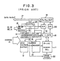
- FIG.3 shows the overall construction of a typical flash memory device.
- the device includes a memory cell array 11 in which a plurality of memory cell transistors each having a construction of FIG.1 are arranged in rows and columns, and the memory cell in the memory cell array 11 is selected in response to address data that is supplied to a row address buffer circuit 12 for activating a row decoder 13 and a column address buffer circuit 14 for activating a column decoder 15.
- the row decoder 13 selects a word line WL in response to the row address data latched in the row address buffer circuit 12 while the column decoder 15 controls a column selection gate 16 to select a bit line BL in response to the column address data that is latched in the column address buffer circuit 14.
- a data bus 17 connected to an input/output buffer circuit 18, and the data on the bus 17 is written into a selected memory cell such as the memory cell 11a via a write amplifier 19 and the column selection gate 16.
- the data stored in the selected memory cell is transferred to the input/output buffer circuit 18 via the column selection gate 16 and a sense amplifier 20.
- another buffer circuit 21 that is supplied with an output enable signal /OE, a chip enable signal /CE, and further with a write enable signal /WE, wherein the signal /OE is used for enabling the data output of the input/output buffer circuit 18, the signal /CE is used for the chip selection, and the signal /WE is used for enabling the writing of data into the selected memory cell.
- an erase power supply unit 22 that characterizes the NOR type flash memory device, wherein the power supply unit 22 supplies a predetermined erase voltage when erasing the data from the memory cell array. As is well known, the erasing of data occurs simultaneously for all the memory cells in the memory cell array 11 in the flash memory device.
- a controller 23 is provided in order to control the operation of memory cell device including the erase power supply 22. There, the controller 23 is supplied with data from the data bus 17 as well as an output of the buffer circuit 21 and controls the read/write as well as erase operation of the device.
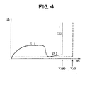
- FIG.4 shows the writing of data into the memory cell transistor of FIG.1, wherein the vertical axis represents the drain current and the horizontal axis represents the drain voltage.
- the voltage V D is applied to. the drain region during the writing process of data, while the voltage V H is applied simultaneously to the control gate.
- the drain current increases in an interval designated as "1" with increasing drain voltage V D , while the drain current decreases suddenly in correspondence to the interval designated as "2" with further increase in the drain voltage V D .
- the injection of electrons into the floating gate electrode occurs.
- an avalanche voltage V ABD an avalanche breakdown occurs in the channel region of the memory cell transistor and the drain current increases steeply. Thereby, an efficient injection of the electrons is achieved into the floating gate.
- the flash memory device generally uses the avalanche voltage V ABD for the voltage V M shown in FIG.2 to achieve an efficient writing of the data.
- the drain voltage V D is clamped at the level V ABD when the foregoing positive control voltage V H is applied to the control gate.
- the drain current changes as shown in the broken line in FIG.4.
- the drain current remains low until a breakdown voltage V JCT is reached.
- V JCT is larger than V ABD by more than one volt.
- the large drain voltage applied to the first memory cell transistor for writing data induces a large electric field between the drain region and the floating gate in the second memory cell transistor.
- the electric charges stored in the second memory cell transistor can dissipate into the drain of the same memory cell transistor and the data held therein is destroyed. This interference of memory cell transistors is known as "disturbance".
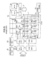
- the conventional flash memory device has suffered from the problem of limited flexibility in the design of redundant construction in that only column redundancy is possible as shown in FIG.5.
- the drawing corresponds to FIG.3 and includes the memory cell array 11 that in turn includes a number of memory cells M 1,1 - M 2,3 provided in correspondence to intersections of word lines WL 1 - WL 2 and bit lines BL 1 - BL 3 .
- the column selection gate 16 includes transfer gate transistors Tsw 1 - Tsw 3 for selecting the bit lines BL 1 - BL 3 respectively.
- the redundant memory cell array 11 CR includes memory cell transistors M 1,4 and M 2,4 having respective drains connected commonly to the bit line BL 4 and the memory cell array 11 CR is activated in response to the output of the redundant decoder 24 that in turn is controlled by a defect detection circuit 25.
- the circuit 25 is supplied with the column address data from a column buffer circuit 14 and compares the same with the address data for defective memory cells stored in a memory device (not illustrated).
- the circuit 25 activates the redundant decoder 24 that in turn selects the redundant bit line BL 4 .
- a redundant memory cell array may be provided as a part of a utility memory cell array that is provided separately from the real memory cell array for various purposes such as testing. In other words, one can use such a memory cell array 11 CR also for testing as will be discussed later with reference to the embodiment of the present invention.
- the floating gate is injected with holes and the memory cell transistors take a permanently turned-on state.
- the transistors M 1,1 - M 1,4 are connected to the bit lines BL 1 - BL 4 , such an erroneous turning-on of the memory cell transistors inevitably causes a erroneous voltage level of the bit lines and the overall operation of the flash memory device becomes defective.
- a utility memory cell block for testing the device.
- Such a utility block is used for example for the purpose of guaranteeing a predetermined number of times for the rewriting of data into the memory cell transistors forming the memory cell array.
- flash memory devices however, erasing of data is achieved in the ordinary, "real" memory cell block each time the data is erased from the utility memory cell block, as long as the memory cell transistors in the real memory cell block share the electric power supply with the memory cell transistors in the utility memory cell block. Thereby, the memory cell transistors in the real memory cell block are erased excessively and the proper read/write operation of the device is no longer possible. In other words, the conventional flash memory devices have suffered from the problem that the test for guaranteeing the number of times the write operation can be achieved properly is impossible.
- a semiconductor memory device characterized by: a memory cell array including a plurality of memory cells arranged in rows and columns, said memory cell array comprising a first group array and a second group array each including a plurality of memory cell blocks, each of said memory cell blocks including a plurality of memory cells and at least one bit line to which said plurality of memory cells are connected, each of said memory cell blocks in said second group array having a corresponding memory cell block in said first group array, so that said memory cell block in said first group array and said memory cell block in said second group array and corresponding to each other form an adjoint pair; first addressing means supplied with address data for selecting a memory cell block in said first group array in response thereto, said first addressing means further selecting a bit line in said selected memory cell block; second addressing means supplied with said address data for selecting a memory cell block in said second group array in response thereto, said second addressing means further selecting a bit line in said selected memory cell block; selection control means supplied with said address data for controlling said first
- FIG.6 shows the principle of a flash memory which is useful for understanding the present invention.
- the flash memory includes the memory cell array schematically illustrated in the form of the memory cell transistor 11a, wherein the control circuit 23 of the flash memory as represented schematically in FIG.3 includes a signal generator 233 that is supplied with an output signal PGM of the buffer circuit 21 in response to the write enable signal /WE when writing data. There, the circuit 233 produces a first control signal PGMR and a second control signal PGMC in response to the signal PGM, wherein the signal PGM causes a transition to the high level state during the interval in which the writing of data is achieved.
- the circuit 231 in turn produces a gate voltage V G in response to the signal PGMC and the voltage level of the control gate represented as "G" in FIG.6 is held at a high level state corresponding to the voltage V H during the interval in which the signal PGMC assumes the high level state.
- the circuit 232 in turn produces a drain voltage represented as V D in FIG.6 such that the drain voltage V D is held at the level V M during the high level interval of the signal PGMC.
- the gate voltage V G is set to the high level state V H before the drain voltage V D rises to the high level state V M , and the gate voltage V G maintains the high level state even after the drain voltage V D has caused a transition to the low level state.
- FIG.7 shows the circuit diagram of the circuit 233.
- the circuit 233 includes an inverter 233a supplied with the signal PGM and produces an output as a logic inversion of the signal PGM.
- the output of the inverter 233a is supplied on the one hand to a NAND gate 233d and on the other hand to a NOR gate 233e, wherein the NAND gate 233d and the NOR gate 233e form a flip-flop circuit that includes a first feedback path for feeding back the output of the NAND gate 233d to another input terminal of the NOR gate 233e via an inverter 233b and a second feedback path for feeding back the output of the NOR gate 233e to another input terminal of the NAND gate 233d via an inverter 233c.
- FIGS.8(A) - 8(C) show the output signals PGMR and PGMC with a timing relationship as shown in FIGS.8(A) - 8(C), wherein FIG.8(A) shows the waveform of the signal PGM, FIG.8(B) shows the waveform of the signal PGMR, and FIG.8(C) shows the waveform of the signal PGMC.
- PGMR rises substantially in synchronization to the leading edge of the PGM, while the leading edge of the PGMC is delayed with respect to the leading edge of the PGM by an interval td 1 , wherein the interval td 1 corresponds to the delay caused by the NAND gate 233d and the inverter 233b.
- the delay td 1 is set such that the rise of the drain voltage V D occurs after the rise of the gate voltage V G in the circuit 233 of FIG.7.
- the PGMC causes a transition to the low level state substantially in synchronization with the trailing edge of the PGM, while the trailing edge of the PGMR appears after a delay of td 2 with respect to the trailing edge of the PGM, wherein the delay td 2 is determined by the delay caused by the NOR gate 233e and the inverter 233c.
- the delay td 2 is determined such that the gate voltage returns after the drain voltage returns to the low level state. This indicates that the gate voltage V G is held at the high level state V H for a while, even when the drain voltage V D has caused a transition to the low level state.
- FIG.9 is a block diagram similar to FIG.5 and shows the construction of the memory device that uses the foregoing circuit 233 for the formation of the signals PGMR and PGMC.
- those parts corresponding to FIG.5 are designated by the same reference numerals and the description will be omitted.
- the PGMR is supplied to a row selection power supply circuit 13A that produces the output signal V G in response to the high level state of the PGMR, and the signal V G is supplied to the row decoder 13 to which the row address data is supplied simultaneously.
- the row decoder 13 selects a word line such as WL 1 in response to the row address data supplied thereto and supplies the gate voltage V G to the selected word line WL 1 .
- a column power supply circuit 15A that is supplied with the PGMC, wherein the circuit 15A activates the column decoder 15 in response to the high level interval of the PGMC.
- the PGMC is supplied also to a drain power supply circuit 19A that forms a part of the write amplifier 20, and the drain voltage V D is controlled as already described with reference to FIGS. 8 (A) - 8(C) in response to the PGMC.
- the drain voltage V D never increases beyond the avalanche voltage V ABD , and the problem of the disturbance is successfully eliminated.
- the delay times td 1 and td 2 are determined to be larger than the difference between the signal delay occurring in the conductor strip that transfers the signal PGMR from the circuit 233 to the control gate of the selected memory cell transistor and the signal delay occurring in the conductor strip for transferring the signal PGMC from the circuit 233 to the drain region of the selected memory cell transistor.
- the conductor strip used for carrying the signal PGMR is generally formed of polysilicon and the delay occurring in the conductor strip for transferring the signal PGMR is generally larger than the delay occurring in the conductor that transfers the signal PGMC.
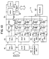
- FIG.10 shows a flash memory device having row redundancy.
- FIG.10 those parts corresponding to the parts already described with reference to FIG.5 or FIG.9 are designated by the same reference numerals and the description thereof will be omitted.
- the memory cell array 11 includes a row and column formation of the real memory cell transistors M 1,1 - M 3,3 that are selected by the row decoder 13 and the column decoder 15 similarly to the device of FIG.5, wherein it will be noted that there is provided an additional memory cell block that includes memory cell transistors M 3,1 - M 3,3 also in the memory cell array 11 as a row redundant memory cell block, and a defect detection circuit 34 for detecting the selection of a defective word line and a redundant word decoder 35 for selecting a redundant word line such as WL 3 in response to the output of the defect detection circuit 34, are provided for activating the row redundant memory cell block.
- the phrase "defective word line” means a word line to which a defective memory cell transistor is connected.
- an additional, utility memory cell block connected to a word line WL 4 that is selected by a utility word decoder 36.
- the utility memory cell block includes memory cell transistors M 4,1 - M 4,3 and is used for testing the operation of the flash memory device.
- the device in order to avoid the problem of the excessive erasing of information from non-selected memory cells described previously in relation to the problem of row redundancy in the flash memory devices as well as the problem of the erase disturbance phenomenon, the device applies a large negative voltage -V E selectively to the control electrode of the memory cell transistor from which the information is to be erased, such that a dissipation of the electrons occurs from the floating gate to the substrate as indicated in FIG.11. There, a positive voltage V L corresponding to the voltage V L described with reference to FIG.2 is applied to the substrate of the device.
- a zero or positive voltage is applied to the control electrode of the non-selected memory cells to avoid dissipation of the electric charges from the floating gate of the non-selected memory cells to the substrate.
- the voltage V E is set to -9 volts.
- the dissipation of the electrons may be caused from the floating gate to the source region by applying the voltage V E to the control gate and the voltage V L to the source simultaneously as indicated in FIG.12.
- the device of FIG. 10 employs a construction of the row address buffer circuit 12 as shown in FIG.13, wherein only a part of the circuit is illustrated. It should be noted, on the other hand, that the power supply 22 is no longer used for the erasing purpose. Thus, the power supply 22 merely produces zero volt or a voltage corresponding to the level V H .
- the circuit 12 includes a NOR gate 12a that is supplied on the one hand with a control signal PD that is set to the low level state during the operational state of the flash memory device and on the other hand with an address signal included in the multiple-bit address data, wherein the output of the NOR gate 12a is supplied to a first input terminal of another NOR gate 12c via an inverter 12b. Further, the output of the NOR gate 12a is supplied to an input terminal of a NOR gate 12d.
- both the NOR gate 12c and the NOR gate 12d are supplied with an output of the defect detection circuit 34 simultaneously, wherein the defect detection circuit 34 produces the output such that the output of the circuit 34 assumes a high level state when a selection of the defective word line is made.
- the output of the circuit 34 is of course set to the low level state.
- both the output signal AD of the NOR gate 12c and the output signal /AD of the NOR gate 12d are set to the low level state. It should be that the circuit of FIG.13 is provided in number corresponding to the number of the bits of the address data to form the address buffer circuit 12.
- FIG.14 shows the construction of the row decoder 13, wherein the row decoder 13 includes a NAND gate 13a that receives the address data from the row address buffer circuit 12.
- the output of the row decoder 13 is supplied, via an n-channel MOS transistor 13b and a p-channel MOS transistor 13g both urged to a turned-on state by the supply voltages V cc and V ss respectively, to a latch circuit that includes a p-channel MOS transistor 13h and an n-channel MOS transistor 13c connected in series between a power supply voltage V DD2 and another power supply voltage V DS2 .
- the latch circuit further includes a p-channel MOS transistor 13i and an n-channel MOS transistor 13d connected in series between the foregoing power supply voltages V DD2 and V DS2 , wherein the transistors 13h and 13i as well as the transistors 13c and 13d are connected such that the voltage at the node between the transistors 13h and 13c is supplied to the respective gates of the transistors 13i and 13d and such that the voltage at the node between the transistors 13i and 13d is supplied to the respective gates of the transistors 13h and 13c.
- the output of the latch circuit is obtained at the node between the transistors 13i and 13d and is supplied to the gate of an n-channel MOS transistor 33e that is connected in series to another n-channel MOS transistor 13f.
- the transistors 13e and 13f are connected in series between a supply voltage V DS1 and a supply voltage V DS2 , wherein the transistor 13f is supplied with the output of the transistor 13g directly.
- the voltage V cc is typically set to +5 volts while the voltage V ss is set typically to zero volt.
- the voltages V DD1 and V DS2 are set, in the erasing mode, to the foregoing negative voltage V E that is applied to the control gate of the memory cell transistor for erasing data therefrom.
- the voltages V DD2 and V DS1 correspond to the voltage V L that is supplied to the substrate in the erasing scheme of FIG.11. In the erasing mode shown in FIG.12, the voltage V L is supplied to the source region.
- the circuit of FIG.14 outputs the control voltage on the selected word line WL i such that the control voltage is set to the level V E in the erasing mode.
- the NAND gate 13a produces a low level output in response to the address data that selects the word line WL i .
- the NAND gate 13a produces a high level output and a control signal having the level V L is outputted on the non-selected word line in response thereto.
- a similar construction is used for the row redundant word line decoder 35 and the utility word line decoder 36.
- the NAND gate 13a is replaced by an inverter 13j that is supplied with the output signal from the defect detection circuit 34.
- an inverter 13k is used in place of the NAND gate 13a in the utility word line decoder 36, wherein the inverter 13k produces an output in response to a test signal supplied thereto.
- the redundant word line WL 3 shown in FIG.10 is selected and the voltage level of the redundant word line WL 3 is urged to the level V E in correspondence to the supply voltage V DD1 , when erasing data.
- the rest of the word lines are all urged to the voltage V L in correspondence to the supply voltage V DS1 .
- the flash erasing operation applied to the row redundant memory cell block does not cause the adversary erasing in the real memory cell block.
- the utility memory cell block connected to the word line WL 4 can be achieved independently from the rest of the memory cells and the problem of the excessive erasing is eliminated.
- FIG.15 shows a circuit 13X for causing the foregoing change of the supply voltage V DD1 in response to the operational mode of the flash memory device.
- the circuit 13X forms a part of the circuit 13 we well as 35 and 36 in the illustration of FIG.10 and includes a p-channel transistor 191 having a source connected to the supply voltage V CC and a p-channel transistor 192 connected in series to the transistor 191. Further, there is provided a p-channel transistor 193 having a source connected to the supply voltage V PP and another p-channel transistor connected in series to the transistor 193. The respective sources of the transistors 192 and 195 are connected commonly to another p-channel transistor 195 that is turned on in response to the erase control signal E. There, the transistors 191 and 192 have respective gates supplied with the write control signal W while the transistors 193 and 194 have respective gates supplied with the complementary write control signal /W.
- the transistors 191 and 192 are turned on while the transistors 193 and 194 are turned off, and the supply voltage V CC is supplied to the transistor 195.
- the control signal E takes a low level state and the supply voltage V CC thus supplied via the transistors 191 and 192 is supplied further through the transistor 195 to the supply terminal V DD1 of the circuit 13 shown in FIG.14.
- the transistors 193 and 194 are turned on while the transistor 191 and 192 are turned off, and the high positive supply voltage V PP is supplied to the terminal V DD1 via the transistor 195 that is turned on in response to the non-erasing mode.
- the circuit of FIG.15 includes a number of p-channel transistors 196, 197, 198, . . . connected to form a diode wherein the transistors 196, . . . are connected in series to the supply voltage V SS via an n-channel transistor 195A that is turned on and turned off in response to the erase control signal E.
- the transistor 195A is turned off in response to the low level state of the control signal E, and the transistors 196, 197, 198, . . . are disconnected from the supply voltage V SS .
- the signal E takes a high level state and the transistor 195 turns off while the transistor 195A is turned on.
- the supply voltage V SS is supplied after voltage drop caused by the diode connection of the transistors 196, . . . and a large negative voltage corresponding to V E appears at the terminal V DD1 of the circuit 13 of FIG.14.
- the transistors 196, 197, . . . . are supplied with a clock signal ⁇ and a logic inversion / ⁇ .
- FIG.16 shows a device that has a column redundancy.
- FIG.16 those parts described previously are designated by the same reference numerals and the description thereof will be omitted.
- the memory cell array 11 is divided into a number of memory cell blocks 11 1 . . . 11 m , wherein each memory cell block has a corresponding erase power supply 22 1 , . . . 22 m for supplying the source drive voltage of the flash memory cells such that the flash-erasing of information occurs in each memory cell block independently.
- a redundant memory cell column 11 CR corresponding to the column redundant memory cell array shown in FIG.5, and the redundant memory cell column 11 CR receives the source drive voltage from an independent erase power supply 22 CR . Similar to the device of FIG.5, the redundant memory cell block 11 CR is selected in response to the output from the defect detection circuit 25.
- the redundant decoder 24 is included in the column decoder 15.
- a utility memory cell column 11 UT for testing the device, wherein the memory cell column 11 UT is selected in response to a test signal that is supplied to the column decoder 18 when testing the flash memory device.
- a power supply 22 UT is provided in the memory cell column 11 UT .
- each of the memory cell blocks 11 1 - 11 m includes only the real memory cells. In other words, the memory cell blocks 11 1 - 11 m does not include the redundant memory cell column or utility memory cell column.
- FIG.17 is a circuit diagram showing a part of the device of FIG.16 in detail.
- those parts described previously are designated by the same reference numerals and the description will be omitted.
- bit lines such as the bit lines BL 1 - BL n are grouped to form a memory cell block such as 11 1 , . . . 11 m wherein no redundant memory cell column is included in each memory cell block.
- each memory cell block is activated by a corresponding power supply unit such as 22 1 , . . . 22 m via source supply lines SL 1 - SL m and the flash-erasing or simultaneous erasing of information is achieved within each memory cell block.
- the area that is occupied by the redundant memory cell column can be reduced as compared with the conventional redundant construction wherein the redundant memory cell column is provided in each of the memory cell blocks.
- the erasing of the redundant memory cell block 11 CR does not cause the problem of the excessive erasing in the real memory cell array 11.
- FIG.18 shows a modification of the device of FIG.16 wherein the memory cell array 11 is formed of a single row and column formation of the memory cell transistors M 1,1 - M m,m , wherein the device further includes the utility memory cell column 11 UT .
- the utility memory cell column 11 UT includes memory cells M 1,U , M 2,U , . . . , wherein each of the memory cells M 1,U , . . . have the source region connected commonly by a source supply line SL U to the power supply unit 22 UT that is provided independently from the power supply unit 22 that supplies the source voltage to the memory cell transistors in the memory cell array 11.
- the power unit 22 UT changes the supply voltage in response to the operational mode particularly in the erasing mode as already described with reference to the basic operation of the flash memory device such that the supply voltage is changed independently to the supply voltage that is supplied to the source of the memory cell transistors M 1,1 - M m,m from the power supply unit 22.
- the utility memory cell column 11 UT of FIG.18 may be used for example for the testing purpose for guaranteeing the number of times the device is capable of rewriting as already described, wherein the device of the present device is advantageous in the point that the erasing operation of the utility memory cell column 11 UT does not affect at all the state of the real memory cell array 11 because of the use of the separate, independent power supply unit 22 UT for effecting a connection of the bit line BL U to the sense amplifier 20.
- a test control signal is supplied to the gate of the column gate transistor (Tsw) UT .
- FIG.19 a fourth device useful for understanding the present invention will be described with reference to FIG.19, wherein those parts corresponding to the parts described previously are designated by the same reference numerals and the description will be omitted.
- the memory cell array 11 is divided into a plurality of memory cell blocks 11 1 - 11 m , wherein the device further includes a redundant memory cell column 11 CR and a utility memory cell column 11 UT .
- Each memory cell block includes a plurality of bit lines connected commonly to a source of a MOS transistor that forms the switch S 1 to be described below.
- the memory cell blocks 11 1 - 11 m as well as the memory cell columns 11 CR and 11 UT are connected to the sense amplifier 20 and the write amplifier 19 via a common output line DL wherein there are provided switches SW 1 - SW CR for controlling the connection between the bit lines in the memory cell blocks 11 1 - 11 m and the output line DL as well as the connection between the bit lines included in the memory cell columns 11 UT and 11 CR and the output line DL.
- the switches SW 1 - SW CR are supplied with a control signal S 1 - S CR and are activated in response thereto.
- each of the memory cell blocks and memory cell columns 11 1 - 11 CR has a corresponding power supply unit 22 1 - 22 CR for supplying the source voltage to the memory cell transistors included therein.
- the power supply units 22 1 - 22 CR are designed to have respective output power or supply current that is optimized based upon the number of the memory cells included in the corresponding memory cell block or memory cell column.
- the optimization of the current output ability of the power supply units will be described in brief.
- the erasing of information is achieved by removing electric charges from the floating electrode gate in the form of tunneling current.
- holes are created as a result of formation of the tunneling current and the holes thus created penetrate into the gate insulation film located under the floating gate.
- the operational characteristics of the memory cell transistor are deteriorated.
- such an accumulation of the holes in the gate insulation film is one of the major reasons that limits the lifetime of a flash memory device.
- FIG.20 shows the change of the source current with the source voltage applied to the memory cell transistor shown in FIG.1 during the erasing operation, wherein FIG.21 shows the condition that the erasing characteristics of FIG.20 are obtained.
- the memory cell transistor shown in FIG.1 is biased according to the erasing condition as set forth in FIG.2, and a gate current that flows from the floating gate 3 to the source 6 is measured by applying a d.c. voltage to the floating gate.
- the source current I S increases gradually with increasing source voltage V S until a critical voltage V SC is reached above which the source current I S increases steeply due to avalanche breakdown.
- the erasing of the information is achieved during this interval where the source current I S increases gradually with the source voltage V S .
- the critical voltage V SC is attained, it will be noted that a gate current starts to flow from the floating gate electrode 3 to the source region 6 as indicated in FIG.20.
- the source voltage and hence the source current that is employed during the erasing operation is adopted in each of the memory cell blocks and the memory cell columns in the configuration as shown in FIG.19.
- the utility memory cell column 11 UT in particular, it is aimed to supply the source voltage such that the same source current flows in each memory cell transistor therein during the erasing operation as in the memory cell transistors in the memory cell blocks 11 1 - 11 m . Otherwise, the result of the rewriting test conducted on the utility memory cell column becomes useless.
- FIGS.22(A) - 22(D) show the construction of the power supply units 22 1 - 22 UT , wherein the circuits shown therein have generally a similar connection.
- the power supply unit 22 1 has an input terminal 22a to which an erase control signal ERS3 is supplied.
- the erase control signal ERS3 thus supplied is further transferred to the gate of a p-channel MOS transistor 22d and an n-channel MOS transistor 22c connected in series between a supply voltage source V PP and the ground via a transfer gate transistor 22b that is urged to the turned-on state by a supply voltage V CC supplied to the gate thereof.
- the output obtained at the intermediate node between the transistors 22c and 22d is supplied on the one hand to the gate of a p-channel MOS transistor 22c that is connected between the supply voltage source and a node 22g connected to the gate of the transistors 22c and 22d, and on the other hand to the gate of the transistors 22h and 22j that are connected in series between the power supply V PP and the ground with a transistor (22i) 1 interposed therebetween.
- the transistor (22i) 1 has a gate and a source connected with each other to form a constant current circuit, and the output of the circuit 22 1 is obtained at the node where the transistor (22i) 1 is connected to the transistor 22 j .
- the output transistor (22i) 1 has a gate width W 1 that is adjusted to supply an optimized output current to the source line SL 1 that is connected to the source of the memory cell transistors.
- the node 22g takes a low level state in response to the low level state of the erase control signal ERS 1 that indicates the non-erasing mode, and the p-channel transistor 22d is turned on while the n-channel transistor 33c is turned off. Thereby, the node 22f is urged to the level V PP and the p-channel transistors 22e and 22h are turned off while the n-channel MOS transistor 41 is turned on. As a result, the source line SL 1 is set to zero volt.
- the erase signal ERS 1 is set to the high level state in correspondence to the erasing operation, on the other hand, the level of the node 22g is urged to the Vcc level and the transistor 22c is turned on. As a result, the level of the node 22f approaches to zero and the p-channel transistors 22e and 22h are turned on while the n-channel transistor 22j is turned off.
- the level of the node 22g rises to the level V PP , and the p-channel transistor 22d is turned off.
- the level of the node 22f is urged to zero volt and the supply voltage V PP is supplied to the source line SL 1 via the p-channel transistor 22h and the n-channel transistor (22i) 1 .
- the erasing of information is achieved.
- a similar operation is achieved in the other circuits shown in FIGS.20(B) - 20(D). As the operation for these circuits is obvious, further description for the supply circuits of FIGS.20(B) - 20(D) will be omitted.
- the transistor (22i) 1 acting as a constant current source has a gate width W 1 that is set to provide a source current that is sufficient to erase the information from the memory cell transistors included in the memory cell block 11 1 .
- the gate width W 1 is set in accordance with the number of the memory cell transistors that are included in the memory cell block. More specifically, the gate width W 1 is set such that the power supply circuit 22 1 has a capability of supplying the current I SC corresponding to the critical source voltage V SC to each of the memory cell transistors included in the memory cell block 11 1 . See FIG.20. Thereby, an optimum source current is supplied to the memory cell transistors in the memory cell block 11 1 when erasing information.
- the output transistors (22i) m , (22i) UT and (22i) CR have respective optimum gate widths W m , W UT and W CR .
- N 1 , N m , N UT and N CR respectively represent the number of the memory cell transistors that are included in the memory cell blocks 11 1 and 11 m and in the memory cell columns 11 UT and 11 CR .
- this device employs the redundant memory cell block 11 CR and the utility memory cell block 11 UT , wherein each of the blocks 11 CR and 11 UT include a plurality of memory cells arranged to form a matrix.
- the memory cell blocks 11 CR and 11 UT include a number of memory cell columns.
- the column decoder 15 is provided commonly to the memory cell blocks 11 CR and 11 UT for selecting a column selection line such as BL 1 , wherein the selection of the column selection line BL 1 is achieved simultaneously in the memory cell block 11 CR and 11 UT .
- the information read out from the selected memory cell column is supplied to the sense amplifier 20 either via a switch circuit SW 1 or SW 2 , wherein the switch circuit SW 1 is closed when the redundant memory cell block 11 CR is activated.
- the switch circuit SW 2 is closed.
- the output of the memory cell block 11 UT and the memory cell block 11 CR is supplied to the sense amplifier 20 selectively.
- FIG.24 shows a more detailed representation of the circuit of FIG.23.
- the redundant memory cell array 11 CR includes memory cell transistors M CR (1,1), . . . arranged in rows and columns while the utility memory cell array 11 UT includes memory cell transistors M UT (1,1), . . . .
- the redundant memory cell transistors M CR (1,1), . . . are connected to column lines (CL 1 ) CR , . . . while the utility memory cell transistors M UT (1,1), . . . are connected to column lines (CL 1 ) UT .
- the column lines (CL 1 )CR, . . . are selected by column gate transistors (Tsw1) CR , . . .
- the column selection lines BL 1 , . . . are connected commonly to the corresponding column gate transistors (Tsw1) CR , . . . for the redundant memory cell array 11 CR and to the column gate transistors (Tsw1) UT , . .
- the drains of the column gate transistors are connected to a common drain line (DL) CR and a common drain line (DL) UT , wherein the drain line (DL) CR is connected to the sense amplifier 20 via a transfer gate transistor Tr 1 that is supplied with a control signal RED for activating the redundant memory cell array and acts as the switch SW 1 , while the drain line (DL) UT is connected to the sense amplifier 20 via a transfer gate transistor Tr 2 that is supplied with a control signal TEST for activating the testing in the utility memory cell array and acts as the switch SW 2 .
- control signal RED is produced in response to the column address data upon the selection of a defective bit line. See for example the circuit of FIG.5, wherein the signal RED is produced by the redundant decoder 24.
- control signal TEST is produced externally upon the running of the test procedure.
- the memory cell transistors are selected simultaneously in the redundant memory cell array 11 CR and the utility memory cell array 11 UT , wherein the information signals thus read out from the selected memory cell transistors are selected further by the transistors Tr 1 and Tr 2 in response to the control signals RED and TEST supplied thereto.
- control signals RED and TEST are supplied also to the column driver 15a via an OR gate 15b for activating the same.
- FIG.25 shows the construction of the OR gate 15b as a part of the driver circuit 15a.
- the driver circuit 15a includes a number of circuit blocks 40 0 - 40 3 provided in correspondence to the column selection lines BL 1 - BL 4 , wherein each of the circuits blocks 40 0 - 40 3 have the same construction and only the circuit block 40 0 will be described.
- the circuit block 40 0 includes a depletion mode n-channel MOS transistor 41 0 and an enhancement mode n-channel MOS transistor 43 0 connected in series, wherein the drain of the transistor 41 0 is connected to the supply voltage V cc , while the source and drain of the transistor 41 0 are connected to each other at a node 47 0 . Further, a selection signal /(A n + A m ) produced as a result of the decoding in the decoding part of the column decoder 15 is supplied to the gate of the transistor 43 0 , wherein the transistor 43 0 has a source that is connected to the ground either via a transfer gate transistor 45 or the transfer gate transistor 46.
- the transistors 45 and 46 form a part of the OR gate circuit 15b.
- the transistor 45 or 46 is turned on and the transistor 43 0 supplies an output signal to the foregoing node 47 0 in response to the selection signal /(A n + A n+1 ) supplied to the gate of the transistor 43 0 , provided of course that the transistor 45 or 46 is turned on.
- the output signal at the node 47 0 is supplied further to the gate of the p-channel transistor 42 0 and simultaneously to the gate of the n-channel transistor 44 0 connected in series thereto, wherein the transistors 42 0 and 44 0 form an output stage circuit of the circuit block 40 0 and connected between the supply voltage V cc and the ground. There, the output stage circuit outputs the column selection signal on the column selection line BL 1 that is connected to the intermediate node between the transistors 42 0 and 44 0 .
- each of the circuit blocks 40 1 - 40 3 conducts the same operation in response to various combinations of the input signals such as /(/A n + A n+1 ), /(A n + /A n+1 ) and /(/A n + /A n+1 ), wherein the drain of the transistors 43 0 - 43 3 are connected commonly to the transistors 45 and 46.
- the area of the semiconductor chip that has been occupied by the column decoder can be reduced substantially, as the redundant memory cell array 11 CR and the utility memory cell array 11 UT use the same column decoder. Further, it should be noted that this feature is not only valid in the flash memory devices but also to other conventional semiconductor memories such as dynamic random access memories.
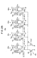
- FIG.26 corresponds to a modification of the construction of the circuit of FIG.5.
- the circuit of FIG.26 is intended for testing the erasing operation of the flash memory device and includes a write control circuit 25a.
- the conventional circuit of FIG.5 selects a redundant memory cell column when a defective memory cell column is addressed. Thereby, the writing of the defective memory cell column is not made and the memory cells included in the defective memory cell column become excessively erased state upon the flash-erasing process. In the circuit of FIG.5, this excessive erasing of the defective column does not cause any problem, as the selection of such a defective column is prohibited by the column gate transistor such as Tsw 3 .
- the foregoing construction has a drawback in that the writing of information into the redundant memory cell column is not possible in the absence of information about the defective memory cells. More specifically, the writing of data "0" into the memory cells before erasing for avoiding the excessive erasing cannot be conducted for the redundant memory cells. Thereby, the erasing test conducted upon the real memory cells connected to real bit lines BL 1 - BL n inevitably causes an excessive erasing state in the redundant memory cells connected to the redundant bit lines (BL 1 ) CR - (BL 21 ) CR .
- the circuit of FIG.26 employs a write control circuit 25a that activates the redundant column decoder 24 via an OR gate 25b in response to a redundant selection signal RED ACTIV. Simultaneously, the circuit 25a deactivates the column decoder 15 also via the OR gate as well as via an inverter 25b.
- the circuit of FIG.26 achieves the usual column redundancy controlled by the defect detection circuit 25 via the OR gate 25b.
- a control signal W is supplied to the decoders 13, 15 and 24 such that the signal W has a high level state corresponding to the voltage V PP for setting the memory cell transistors in the real memory cell array as well as in the redundant memory cell array to the state ready for writing information.
- the control signal RED ACTIV is set to the low level state and the writing of the data "0" is achieved into the memory cell transistors in the real memory cell array while prohibiting the wiring of the data "0" into the redundant memory cell arrays
- the control signal RED ACTIV is set to the high level state and the writing of the data "0" is conducted into the redundant memory cell transistors while prohibiting the writing into the real memory cell transistors.
- the erase power supply 22 is activated in response to the erase control signal E, and the flash-erasing of information is achieved for the entirety of the memory cells including the real memory cells and the redundant memory cells.
- FIG.27 shows an example of the construction of the circuit 25a shown in FIG.26, wherein the circuit includes p-channel MOS transistors 251 and 252 as well as an n-channel MOS transistor 253 connected in series with each other between the two supply voltages V cc and V ss , wherein the transistors 252 and 253 have respective gates connected each other to the supply voltage V cc .
- the control signal RED ACTIV is supplied to a terminal P in connected to the drain of the transistor 251 and takes a voltage level V HH that exceeds the supply voltage V CC when the signal RED ACTIV is in the high level state.
- the p-channel transistor 252 is turned on and the n-channel transistor 253 is turned on and a voltage at the node between the transistors 252 and 253 is supplied to an inverter circuit that includes a series connection of the p-channel transistor 254 and an n-channel transistor 255. Further, the output of the inverter is supplied to a next inverter that includes a series connection of a p-channel transistor 256 and an n-channel transistor 257, and the output control signal to be supplied to the OR gate 25b is obtained at the intermediate node between the transistors 256 and 257.
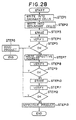
- FIG.28 shows a flowchart for separating defective products from good products based upon the foregoing erasing test operation.
- the writing of data "0" is conducted into the real memory cells in a first step 1 by activating the column address buffer circuit 14 and the column decoder 15.
- the writing of the data "0" is conducted into the redundant memory cells in a step 2 by activating the redundant decoder 24 via the write control circuit 25a.
- an erasing process is achieved in a step 3 by activating the erase power supply unit 22. Thereby, the flash erasing of information is achieved for the entirety of the memory cells in the real and redundant memory cell arrays.
- the result of the flash-erasing process of the step 3 is verified by reading the content of information of the memory cells in the real and redundant memory cell arrays.
- the device is judged in a step 6 as being a good product.
- the addresses of the defective memory cells that show the erroneous erasing are written into a memory that is provided in the defect detection circuit 25 in a step 7. Further, a verification process is conducted in a step 8 for verifying the column redundant operation of the device based upon the address of the defective memory cells.
- step 9 When it is confirmed in a step 9 that the column redundant operation is satisfactory, the step 6 is conducted and the device is identified as being a good product.
- a step 10 is conducted to achieve the erasing procedure again.
- the operation of the device is verified in a step 11 by reading the content of the memory cells.
- the result of the verification process of the step 11 is checked in a discrimination step 12 to discriminate whether the device achieves the satisfactory operation or not. If the result in the step 12 is YES, the step 6 is conducted and the device is identified to be a good product.
- a step 13 is conducted wherein the device is identified as being a defective product.
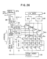
- FIG.29 shows a device to which the present invention (described later) can be applied.
- this device is based upon a concept similar to FIG.23 and uses a common column decoder for the real memory cell array 11 and redundant memory cell arrays 11 CR1 - 11 CRn .
- the construction for realizing the column redundancy is substantially simplified.
- the circuit of FIG.29 is designed for the column redundancy instead of the device of FIG.23 that is designed for the testing of the redundant memory cell column and the utility memory cell column, there exists a difference between the circuit of FIG.29 and the circuit of FIG.23 as will be described below.
- the redundant decoder 24 used in the construction of FIG.5 is no longer used.
- the column decoder 15 is used commonly for the real memory cell array 11 and the redundant memory cell arrays 11 CR1 - 11 CRn , and the selection of a bit line such as B 1 in the memory cell array 11 causes a simultaneous selection of the bit lines in the redundant memory cell arrays.
- a switch circuit 16A such the switch circuit 16A is activated in response to a control signal S comp outputted from the defect detection circuit 25.
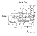
- FIG.30 shows the essential part of the circuit of FIG.29, wherein it will be noted that the column decoder 15 includes a number of decoding circuits DC 0 , DC 1 , . . . corresponding respectively to the column gate transistors T a , T b , T c , T d , . . . , wherein the decoding circuit DC 0 selects the bit line B 0 while the decoding circuit DC 1 selects the bit line B 1 .
- the transistors T a , T b , . . . correspond to the previously described column gate transistors Tsw 1 , . . . and form the 16, 16 CR1 , 16 CR2 , . . . .
- the defect detection circuit 25 raises the level of one of the control signals S B0 , S B1 , . . . that are supplied therefrom to the decoding circuits DC 0 , DC 1 , . . . , selectively based upon the result of comparison of the supplied column address data with the address data of the defective memory cell columns.
- a decoder such as DC 1 is selectively activated. In this case, the bit lines B 1 and B 1s are selected simultaneously.
- the defect detection circuit 25 supplies the control signal S comp to the switch circuit 16A.
- the switch circuit 16A includes transfer gate transistor T e and T f wherein the transistors T e and T f are turned on and turned off complementarily in response to the control signal S comp .
- the transistor T e is provided in correspondence to the real memory cell array 11 and the bit lines B 0 , B 1 , . . . in the real memory cell array 11 are connected commonly to the transistor T e via respective column gate transistors T a , T b , . . . .
- the redundant bit lines B 0S , B 1S of the redundant memory cell arrays are connected commonly to the transistor T f that corresponds to the redundant memory cell array.
- FIG.31 shows the construction of the decoding circuit such as DC 0 , wherein it will be noted that p-channel transistors T j , T g , T n , . . . , T i are connected in series between the supply voltage V CC and the supply voltage V SS , wherein the transistors T g , T n , . . . T i are supplied with a logic combination of the column address signals and cause a transition to the turned-on state in correspondence to a particular logic combination thereof, while the transistor T j acts as a constant current source and supplies a drive current to a node N where the transistor T j and the transistor T g are connected with each other.
- the output obtained at the node N as a result of the foregoing decoding action of the transistors T g - T i is supplied to an output inverter that includes a series connection of a p-channel MOS transistor T OUT and an n-channel MOS transistor T OUT ' as usual, wherein there is provided an additional transistor T k such that the transistor T k is connected between the node N and the ground G.
- the transistor T k is supplied with the foregoing signal S B0 or S B1 from the defect detection circuit 25 at the gate thereof and urges the level of the node N at the low level state in response to the high level state of the control signal S B0 or S B1 , irrespective of the logic combination of the column address signal.
- the output level of the output inverter is forced to the high level state.
- the control signals S B0 and S B1 from the defect detection circuit 25 overrides the result of the decoding in the column decoder, and the selection of the redundant bit line occurs irrespective of the decoding operation in the column decoder 15, as long as the column address data specifies a defective memory cell column.
- FIG.32 shows an embodiment of the present invention, which is a modification of the device of FIG.29, wherein the real memory cell array 11 is divided into a plurality of memory cell blocks 11 1 and 11 2 .
- redundant memory cell blocks 11 CR1 and 11 CR2 are provided.
- the bit lines in the memory cell block 11 1 are selected by a column gate switch circuit 16 1
- the bit lines in the memory cell block 11 2 are selected by a column gate switch circuit 16 2
- the bit lines in the memory cell block 11 CR1 are selected by a column gate switch circuit 16 CR1
- the bit lines in the memory call block 11 CR2 are selected by a column gate switch circuit 16 CR2 .
- a redundant decoder 24A similar to the redundant decoder 24 of FIG.5 is used for activating the column gate switches 16 1 , 16 2 , 16 CR1 and 16 CR2 , wherein the column gate switches 16 1 and 16 2 are controlled by the column decoder as usual.
- the column gate switches 16 CR1 and 16 CR2 are activated commonly by a control signal SR SEL produced by a redundant decoder 24A.
- the redundant decoder 24A is supplied with the column address data from the column buffer 14 simultaneously to the column decoder 15 and controls the decoder 15 by supplying a control signal S INH such that the operation of the decoder 15 is prohibited when there exist a bit line in the real memory cell 11 1 or 11 2 and also a bit line in the redundant memory cell 11 CR1 and 11 CR2 in correspondence to a given column address.
- the decoder 24A prohibits the operation of the decoder 15 and selects redundant bit lines in the memory cell arrays 11 CR1 and 11 CR2 . Thereby, the reading of information is achieved either from the real memory cell array or from the redundant memory cell array.
- the reading is achieved either from the memory cell array 11 1 or 11 CR1 , and the information thus read out is supplied to the transistor T e that forms a part of the switch circuit 16A.
- the reading of information is achieved either from the memory cell array 11 2 or from the redundant memory cell array 11 CR2 and the information thus read out is supplied to the transistor T f included in the switch circuit 16A.
- the decoder 24A further produces control signals SR 1 and SR 2 and activates either the transistor T e or the transistor T f in response to the logic combinations of the signals SR 1 and SR 2 via a control circuit 24B.
- control circuit 24B As a result, reading of information is achieved selectively from either of the memory cell arrays 11 1 , 11 2 , 11 CR1 and 11 CR2 .
- FIG.33 shows the construction of the circuit 24B.
- the circuit 24B includes a NOR gate 241 and a NAND gate 242 connected in series wherein the supply voltage V SS is supplied to one input terminal of the NOR gate 241 while the most significant bit A MSB of the column address data is supplied to the other input terminal.
- the output of the NAND gate 242 is supplied to a NOR gate 243, wherein the NOR gate 243 is supplied with the control signal SR 1 at the other input terminal. Further, the output of the NOR gate 243 is supplied to a first input terminal of a NOR gate 244 that is supplied also with the control signal SR 2 at the other input terminal.
- the output of the NOR gate 244 is supplied to the transistor T e as a control signal SEL and further to the transistor T f via an inverter 245 as a control signal SEL x .
- the output signals SEL and SEL x are produced as a result of the logic combination of the signals A MSB , SR 1 and SR 2 .
- the signal SEL takes the same logic level as the signal A MSB when the signals SR 1 and SR 2 both have the low level state in correspondence to the non-redundant operation.
- the logic level of the output signal SEL is urged to the high level state when the signal SR 1 has the high level state.
- the signal SEL is urged to the low level state when the signal SR 2 has the high level state.
- the present embodiment as described with reference to FIGS.32 and 33 is also effective for simplifying the construction of the memory device by controlling the redundant memory cell arrays 11 CR1 and 11 CR2 by the same control signal SR SEL produced by the same decoder circuit 24A.
- V H very high voltage
- 12 volts has to be applied to the drain region of the memory cell transistor.
- V H very high voltage
- the application of such a high voltage to the n + -type source region tends to invite a breakdown at the p-n junction between the source region and the substrate.
- the application of such a very large voltage to the source region tends to induce a depletion region in the substrate immediately under the gate insulation film, and the large electric field associated with such a depletion region may cause to flow a tunneling current from the valence band to the conduction band.
- the same goal as the device of FIG. 10 is achieved by applying simultaneously a positive voltage to the substrate and a negative voltage to the control gate electrode, when erasing information, with the same magnitude such that no extraordinary large voltage appears between the active parts of the memory cell transistors as well as the peripheral transistors forming the peripheral circuit.
- the flash memory is constructed on a p-type substrate 110 that is defined with a memory cell region wherein memory transistors A and B are formed and a peripheral region wherein a peripheral transistor is formed.
- the memory cell region includes n + -type diffusion regions 126a and 128a respectively serving for the source and drain of the memory cell transistor A and diffusion regions 126b and 128b respectively serving for the source and drain of the memory cell transistor B.
- the memory cell transistors A and B are isolated from each other by a field oxide region 116, and a gate insulation film 118 covers the surface of the device region for the transistors A and B as usual in MOS transistors.
- a floating gate electrode 120a is provided in correspondence to the memory cell transistor A, while a floating gate electrode 120b is provided on the gate insulation film 118 in correspondence to the memory cell transistor B.
- capacitor insulation films 122a and 122b are formed respectively, and control gate electrodes 124a and 124b are provided respectively on the capacitor insulation films 122a and 122b.
- a p-type well 114 surrounded by an external well 112 is formed in the substrate 110 in correspondence to the peripheral region, and n + -type diffusion regions 132 and 134 are formed in the well 114 as the source and drain of the peripheral transistor.
- the gate insulation film 118 is formed also on the surface of the substrate 110 in correspondence to the peripheral transistor and a gate electrode 130 is provided thereon.
- the device of FIG. 34 applies a gate voltage of -10 volts to the control gate electrode 124a and simultaneously applies a substrate voltage of +10 volts. Thereby, a voltage difference of 20 volts is formed between the control gate electrode 124a and the substrate 110, and the electrons accumulated in the floating gate 120a are expelled to the substrate 110 in the form of a Fowler-Nordheim tunnel current.
- a positive voltage of +10 volts is applied simultaneously to the control gate 124b of the memory cell transistor. Thereby, it will be noted that the voltage difference between the control gate 124b and the substrate 110 becomes zero.
- the voltage level of the substrate 110 increases positively also in the peripheral region if the substrate of the peripheral region is not isolated from the rest of the part of the substrate in the form of double well structure shown in FIG.34. There, the positive voltage level applied to the p-type substrate inevitably induces a forward biasing at the p-n junction between the substrate and the diffusion regions 132, 134.
- the FIG. 34 device avoids this problem of adverse forward biasing by providing an n-type well 112 in the substrate 110 in correspondence to the peripheral region and further by forming a p-type well 114 within the n-type well 112. Thereby, the diffusion regions 132 and 134 are formed within the p-type well 114.
- a positive voltage set equal to the positive voltage applied to the substrate 112 is applied to the n-type well 112 such that there occurs no substantial biasing between the p-type substrate 110 and the n-type well. Further, the voltage level of the p-type well 114 is held at zero volt. Thereby, the p-n junction at the interface between the n-type well 112 and the p-type well 114 are reversely biased, and the depletion region developing along the p-n junction effectively isolates the p-type well 114 from the p-type substrate 110.
- the structure of FIG.34 enables the effective erasing of information without providing excessive electric stress to any part of the device.
- the reading and writing of information is achieved similarly to the conventional process shown in FIG.2. Further, when erasing information, one may apply the same positive voltage as the substrate voltage to the source and drain regions of the memory cell transistor.
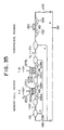
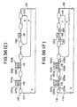
- FIG.35 is a modification of the device of FIG.34, wherein the memory cell region is isolated from the peripheral region by a double well isolation structure.
- the double well includes an outer n-type well 136 and an inner p-type well 138, and the diffusion regions of the memory cell transistors A and B are all formed within the inner p-type well 138.
- FIG.35 further description of the structure of FIG.35 will be omitted.
- the n-type well 112 is formed in the substrate 110 in correspondence to the peripheral region by means of an ion implantation process of an n-type dopant such as As or P followed by a thermal annealing process.
- the p-type well 114 is formed in the n-type well 112 by means of an ion implantation process of a p-type dopant such as B.
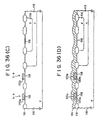
- the surface of the substrate 110 is protected by an oxidation resistant mask (not shown) such as silicon nitride in correspondence to the region where the active part of the device is formed, and the substrate 110 thus masked is subjected to a thermal oxidation process conducted in a wet O 2 environment. Thereby, the field oxide region 16 is formed.
- the mask is removed and the gate oxide film 118 is formed by a thermal oxidation process conducted in a dry O 2 environment. Thereby, the structure shown in FIG. 36(B) is formed.
- a first polysilicon layer is deposited and patterned subsequently to form the floating gate electrodes 120a and 120b respectively in correspondence to the memory cell transistors A and B as shown in FIG.36(C). Further, the structure of FIG.36(C) is subjected to a thermal oxidation process to form the capacitor insulation films 122a and 122b on the floating electrodes 120a and 120b, respectively, and a second polysilicon layer 124 is deposited further thereon. Thereby, the structure shown in FIG.36(D) is obtained.
- the polysilicon layer 124 is patterned to form the control gate electrodes 124a and 124b as well as the gate electrode 130.
- ion implantation of the n-type dopant such as As or P is conducted to form the diffusion regions 126a, 126b, 128a and 128b while using the gate structure as a self-alignment mask in each of the memory cell region and the peripheral region.
- a laminated structure By employing such a laminated structure, it is possible to reduce the thickness of the capacitor insulation film without sacrificing the reliability and anti-leak characteristics of the device. Thereby, an efficient capacitor coupling is achieved between the control electrode and the floating gate electrode.
- the silicon oxide film formed on the polysilicon floating gate shown in FIG.1 tends to form pinholes when the thickness is reduced due to the effect of the grain boundaries in the gate electrode.
- By covering the thin silicon oxide film by a silicon nitride film and form a thin silicon oxide film further on the silicon nitride film one can successfully eliminate the leak from the floating gate while reducing the thickness of the capacitor insulation film.
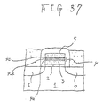
- FIG.37 shows the structure of such a memory cell transistor that has the laminated structure for the capacitor insulation film 4.
- the capacitor insulation film 4 includes a silicon oxide film 4a formed directly on the floating gate electrode 3, a silicon nitride film 4b deposited on the silicon oxide film 4a, and a silicon oxide film 4c formed on the silicon nitride film 4b.
- the power supply unit 22 as well as the power supply units 22 1 , . . . may be a switching circuit for switching the source voltage between a high level voltage such as +12 volts and a low level voltage such as +5 volts, instead of the voltage generator circuit that generates the high voltage output and the low voltage output.
- a high level voltage such as +12 volts
- a low level voltage such as +5 volts
- the power supply unit merely switches the output voltage in response to a control signal.
Description
- The present invention generally relates to semiconductor memory devices, for example a flash-erasable EPROM device or simply a flash memory device.
- In relation to the storage device of computers, there is a continuous demand for a non-volatile semiconductor memory device having a large capacity for storing information. Particularly, the so-called flash-erasable memory device or simply flash memory device has been studied intensively in recent years as an alternative to hard disk devices. In flash memory devices, rewriting of data is possible similarly to the conventional random access memories, while the device can hold the written information even when the electrical power is turned off. Thus, the device is ideal for external storage device of computers just like a hard disk. Further, application to the memory cards is studied. In relation to various applications of the flash memory device, intensive efforts are in progress to improve the properties of the device.
- FIG. 1 shows the structure of a typical memory cell transistor that forms a flash memory device.
- Referring to FIG.1, the memory cell transistor is constructed on a semiconductor substrate 1 and includes a source region 6 and a drain region 7 formed in the substrate 1 similarly to a conventional MOS transistor. On the upper major surface of the substrate 1, a gate insulation film 2 is provided to cover the channel region extending between the source region 6 and the drain region 7, and a gate electrode 3 is formed on the gate insulation film 2 in correspondence to the channel region of the device. Further, a capacitor insulation film 4 is provided to surround the gate electrode 3, and the gate electrode 3 thereby forms a floating gate electrode. Further, an electrode 5 is provided on the floating gate electrode 3 such that the electrode 5 is insulated from the electrode 3 by the capacitor insulation film 4. Thereby, the electrode 5 is used as a control electrode.
- Hereinafter, the operation of a flash memory of the NOR type will be described.
- When writing data, a predetermined drive voltage is applied across the source region 6 and the drain region 7 such that electrons are caused to flow from the source region 6 to the drain region 7. Simultaneously, a large positive voltage is applied to the control electrode 5 to induce a large electric field between the floating gate electrode 3 and the substrate 1. Thereby, the electrons transported along the channel region and accelerated in the vicinity of the drain region 7 are injected into the floating gate electrode 3 through the gate insulation film 2 as hot electrons. Once the electrons are injected, the electric charges associated with the electrons control the conduction of the channel region between the source and drain regions 6 and 7. In other words, one can read the content of the data written into the memory cell transistor by detecting the conduction thereof. When erasing data, on the other hand, a large electric field is induced between the floating gate 3 and the source region 6 by applying a large positive voltage to the source region 6. Thereby, the electrons in the floating gate 3 dissipate into the source region 6 by causing a tunneling through the gate insulation film 2.
- FIG.2 shows the foregoing control scheme of the flash memory device for the writing mode for wiring data into the memory cell, the reading mode for reading data from the memory cell, and the erasing mode for erasing data from the memory cell, wherein the voltage VH is set typically to +12 volts, while the voltage VM may be set to +6 volts. Further, the voltage VL is set to about +5 volts.
- FIG.3 shows the overall construction of a typical flash memory device.
- Referring to FIG.3, the device includes a memory cell array 11 in which a plurality of memory cell transistors each having a construction of FIG.1 are arranged in rows and columns, and the memory cell in the memory cell array 11 is selected in response to address data that is supplied to a row address buffer circuit 12 for activating a row decoder 13 and a column address buffer circuit 14 for activating a column decoder 15. There, the row decoder 13 selects a word line WL in response to the row address data latched in the row address buffer circuit 12 while the column decoder 15 controls a column selection gate 16 to select a bit line BL in response to the column address data that is latched in the column address buffer circuit 14.
- In order to achieve inputting and outputting of data, there is provided a data bus 17 connected to an input/output buffer circuit 18, and the data on the bus 17 is written into a selected memory cell such as the memory cell 11a via a write amplifier 19 and the column selection gate 16. on the other hand, the data stored in the selected memory cell is transferred to the input/output buffer circuit 18 via the column selection gate 16 and a sense amplifier 20. Further, in order to control the read/write operation of the memory device, there is provided another buffer circuit 21 that is supplied with an output enable signal /OE, a chip enable signal /CE, and further with a write enable signal /WE, wherein the signal /OE is used for enabling the data output of the input/output buffer circuit 18, the signal /CE is used for the chip selection, and the signal /WE is used for enabling the writing of data into the selected memory cell.
- Further, there is provided an erase power supply unit 22 that characterizes the NOR type flash memory device, wherein the power supply unit 22 supplies a predetermined erase voltage when erasing the data from the memory cell array. As is well known, the erasing of data occurs simultaneously for all the memory cells in the memory cell array 11 in the flash memory device. In addition, in order to control the operation of memory cell device including the erase power supply 22, a controller 23 is provided. There, the controller 23 is supplied with data from the data bus 17 as well as an output of the buffer circuit 21 and controls the read/write as well as erase operation of the device.
- FIG.4 shows the writing of data into the memory cell transistor of FIG.1, wherein the vertical axis represents the drain current and the horizontal axis represents the drain voltage. As already noted with reference to FIG.2, the voltage VD is applied to. the drain region during the writing process of data, while the voltage VH is applied simultaneously to the control gate.
- Referring to FIG.4, it will be noted that the drain current increases in an interval designated as "1" with increasing drain voltage VD, while the drain current decreases suddenly in correspondence to the interval designated as "2" with further increase in the drain voltage VD. In correspondence to this negative bump of the drain current, the injection of electrons into the floating gate electrode occurs. Further, when the drain voltage VD has reached an avalanche voltage VABD, an avalanche breakdown occurs in the channel region of the memory cell transistor and the drain current increases steeply. Thereby, an efficient injection of the electrons is achieved into the floating gate. Thus, the flash memory device generally uses the avalanche voltage VABD for the voltage VM shown in FIG.2 to achieve an efficient writing of the data. In fact, the drain voltage VD is clamped at the level VABD when the foregoing positive control voltage VH is applied to the control gate.
- On the other hand, when the voltage of the control gate is low or zero in correspondence to an operational state of the device wherein no writing of data occurs, the drain current changes as shown in the broken line in FIG.4. There, the drain current remains low until a breakdown voltage VJCT is reached. In response to the voltage VJCT, a breakdown occurs at the p-n junction between the drain region and the substrate. Generally, the voltage VJCT is larger than VABD by more than one volt. Thereby, there can occur a possibility that the writing of data into a first memory cell transistor can affect the operation of a second memory transistor that shares the power supply line commonly with the memory cell transistor. It should be noted that the large drain voltage applied to the first memory cell transistor for writing data induces a large electric field between the drain region and the floating gate in the second memory cell transistor. Thereby, the electric charges stored in the second memory cell transistor can dissipate into the drain of the same memory cell transistor and the data held therein is destroyed. This interference of memory cell transistors is known as "disturbance".
- Further, the conventional flash memory device has suffered from the problem of limited flexibility in the design of redundant construction in that only column redundancy is possible as shown in FIG.5.
- Referring to FIG.5, the drawing corresponds to FIG.3 and includes the memory cell array 11 that in turn includes a number of memory cells M1,1 - M2,3 provided in correspondence to intersections of word lines WL1 - WL2 and bit lines BL1 - BL3. In FIG. 5, those parts corresponding to the parts described previously are designated by the same reference numerals and the description will be omitted. It will be noted that the column selection gate 16 includes transfer gate transistors Tsw1 - Tsw3 for selecting the bit lines BL1 - BL3 respectively.
- In the memory cell array 11 of FIG.5, it will be noted that there is provided another transfer gate transistor Tsw4 that is activated in response to an output of a decoder 24 for selecting another bit line BL4, and a column redundant memory cell array 11CR is provided in connection to the bit line BL4. There, the redundant memory cell array 11CR includes memory cell transistors M1,4 and M2,4 having respective drains connected commonly to the bit line BL4 and the memory cell array 11CR is activated in response to the output of the redundant decoder 24 that in turn is controlled by a defect detection circuit 25. There, the circuit 25 is supplied with the column address data from a column buffer circuit 14 and compares the same with the address data for defective memory cells stored in a memory device (not illustrated). When the address data indicates the selection of a defective memory cell, the circuit 25 activates the redundant decoder 24 that in turn selects the redundant bit line BL4. It should be noted that such a redundant memory cell array may be provided as a part of a utility memory cell array that is provided separately from the real memory cell array for various purposes such as testing. In other words, one can use such a memory cell array 11CR also for testing as will be discussed later with reference to the embodiment of the present invention.
- In such a conventional flash memory device, it is desirable to provide a row redundant memory cell array in addition to the column redundant memory cell array 11CR for increasing the degree of freedom for saving the defect in the memory cells. However, such a construction of row redundant memory cell array has been generally impossible in flash memory devices. Hereinafter, the reason of this undesirable situation will be examined briefly.
- In flash memory devices, electric charges are removed from the floating gate each time the data stored in the memory cell is erased. As already noted, such an erasing process is conducted by applying a positive voltage to the source region. Thereby, all the memory cells that are connected commonly to the source supply voltage experience dissipation of the electric charges from the floating gate. In other words, the data stored in the memory cells that form the memory cell array of the device are erased simultaneously.
- Another point that requires special attention in flash memory devices is that the dissipation of electrons from the floating gate should be achieved in such a manner that no substantial electric charges remain in the floating gate after the erasing of data has occurred in the memory cell. When the removal of electrons is excessive, the floating gate may charge positively and the memory cell transistor is turned on permanently. In order to avoid this problem of "excessive erasing," it is generally practiced to write data "0" into the memory cell by injecting electrons to the floating gate before each erasing process of data.
- Thus, when a row redundant memory cell array is constructed by modifying the circuit of FIG.5, for example such that the word line WL2 is selected in place of the word line WL1 for saving defective memory cells connected to the word line WL1, the writing of the data "0" does not occur to the memory cells connected to the word line WL1. On the other hand, the removal of the electric charges occurs also in these memory cells in response to the erasing process, as these memory cells are connected also to the erase power supply unit 22. Thereby, the memory cell transistors H1,1 - M1,4 connected to the word line WL1 are inevitably erased excessively as a result of the excessive removal of the electrons to the drain region. When this occurs, the floating gate is injected with holes and the memory cell transistors take a permanently turned-on state. As the transistors M1,1 - M1,4 are connected to the bit lines BL1 - BL4, such an erroneous turning-on of the memory cell transistors inevitably causes a erroneous voltage level of the bit lines and the overall operation of the flash memory device becomes defective.
- In the conventional flash memory devices having the column redundancy as shown in FIG.5, it is proposed to divide the memory cell array into a plurality of blocks each driven by an independent power supply unit such that the simultaneous erasing of data occurs only in each block instead of the entirety of the memory cell array. When the column redundancy is applied to such a device, however, redundant memory cell columns are provided in each block and there arises an inconvenience in that a substantial device area is occupied by the redundant memory cell columns. Thereby, there is a demand to reduce the area of the device that is occupied by the redundant memory cell column.
- In the conventional memory devices such as dynamic random access memories or static random access memories, it has been practiced to provide a utility memory cell block for testing the device. Such a utility block is used for example for the purpose of guaranteeing a predetermined number of times for the rewriting of data into the memory cell transistors forming the memory cell array. In flash memory devices, however, erasing of data is achieved in the ordinary, "real" memory cell block each time the data is erased from the utility memory cell block, as long as the memory cell transistors in the real memory cell block share the electric power supply with the memory cell transistors in the utility memory cell block. Thereby, the memory cell transistors in the real memory cell block are erased excessively and the proper read/write operation of the device is no longer possible. In other words, the conventional flash memory devices have suffered from the problem that the test for guaranteeing the number of times the write operation can be achieved properly is impossible.
- In addition, in the conventional flash memory devices, there has been a problem in that one has to design the device to have a relatively large channel length in correspondence to the relatively large voltage applied to the source region for erasing data from the memory cell transistors, such that a sufficient junction breakdown voltage is secured. On the other hand, such a large channel length inevitably imposes a problem in the miniaturization of the device. Thus, it is desired to reduce the magnitude of the voltage that is applied to the memory cell transistor for erasing information therefrom.
- According to the present invention, there is provided a semiconductor memory device, characterized by: a memory cell array including a plurality of memory cells arranged in rows and columns, said memory cell array comprising a first group array and a second group array each including a plurality of memory cell blocks, each of said memory cell blocks including a plurality of memory cells and at least one bit line to which said plurality of memory cells are connected, each of said memory cell blocks in said second group array having a corresponding memory cell block in said first group array, so that said memory cell block in said first group array and said memory cell block in said second group array and corresponding to each other form an adjoint pair; first addressing means supplied with address data for selecting a memory cell block in said first group array in response thereto, said first addressing means further selecting a bit line in said selected memory cell block; second addressing means supplied with said address data for selecting a memory cell block in said second group array in response thereto, said second addressing means further selecting a bit line in said selected memory cell block; selection control means supplied with said address data for controlling said first addressing means and said second addressing means for prohibiting the selection of a memory cell block in said first group array and a memory cell block in said second group array that form an adjoint pair; said memory cell blocks that form an adjoint pair having respective input/output lines for writing and/or reading information to and from a selected memory cell transistor that are connected commonly to a common input/output line, said common input/output line being provided in number corresponding to the number of said adjoint pairs; and switching means connected on the one hand with said plurality of input/output lines and on the other hand with input/output means for writing and/or reading information to and from a selected memory cell transistor, said switching means being controlled by said selection control means and connecting one of said input/output lines to said input/output means selectively in response to said address data.
- Reference is made, by way of example, to the accompanying drawings wherein Figures 29 to 33 particularly relate to the present invention and wherein the other Figures are useful for understanding the present invention. In the drawings:
- FIG. 1 is a diagram showing the structure and operation of a typical flash memory cell transistor;
- FIG. 2 is a diagram showing the biasing of the flash memory cell transistor for various operations of the memory device;
- FIG.3 is a circuit diagram showing an overall construction of a typical conventional flash memory device;
- FIG.4 is a diagram showing an injection of electrons into a floating gate of the flash memory;
- FIG.5 is a block diagram showing the structure of a conventional flash memory having a column redundancy;
- FIG.6 is a diagram showing a flash memory which is useful for understanding the present invention;
- FIG.7 is a diagram showing the circuit diagram of a control circuit used in the flash memory of FIG.6;
- FIGS.8(A) - 8(C) are diagrams showing the timing for biasing the flash memory of FIG. 6;
- FIG.9 is a block diagram showing the overall construction of a flash memory that uses the control circuit of FIG.7;
- FIG.10 is a block diagram showing the construction of a flash memory having a row redundancy;
- FIG.11 is a diagram showing the biasing scheme used in the flash memory of FIG.10 for erasing information;
- FIG.12 is a diagram similar to FIG.11 for showing an alternative biasing scheme for erasing information in the Fig. 10 device;
- FIG.13 is a circuit diagram showing the construction of a row buffer circuit used in the memory device of FIG.12;
- FIG.14 is a circuit diagram showing the construction of a row decoder used in the memory device of FIG.12;
- FIG.15 is a drive of the row decoder for producing different word line voltages;
- FIG.16 is a block diagram showing the flash memory having a column redundancy, useful for understanding the present invention;
- FIG.17 is a block diagram showing the essential part of the memory device of FIG.16;
- FIG.18 is a circuit diagram showing a modification of the memory device of FIG.16;
- FIG.19 is a circuit diagram showing a modification of the memory device of FIG.16;
- FIG.20 is a diagram showing the erasing characteristics of a typical flash memory cell transistor;
- FIG.21 is a diagram showing the biasing condition that provides the relationship of FIG.20;
- FIGS.22(A) - 22(D) are diagrams showing the optimization of the current supplying capability in the embodiment of FIG.19 in conformity with the number of memory cell transistors included in the memory cell array;
- FIG.23 is a block diagram showing the principle of a flash memory according to a first embodiment of the present invention;
- FIG.24 is a block diagram showing the construction of the flash memory according to the principle of FIG. 23;
- FIG.25 is a circuit diagram showing an essential part of the memory device of FIG.24;
- FIG.26 is a block diagram showing the construction of a flash memory useful for understanding the present invention;
- FIG.27 is a circuit diagram showing a part of the memory device of FIG.26;
- FIG.28 is a flowchart for showing a test process for rejecting defective memory devices;
- FIG.29 is a block diagram showing the construction of a flash memory to which the present invention may be applied;
- FIG.30 is a circuit diagram showing an essential part of the memory device of FIG.29;
- FIG.31 is a circuit diagram showing a part of the memory device of FIG.29;
- FIG.32 is a block diagram showing a modification of the flash memory of FIG.29 as an embodiment of the present invention;
- FIG.33 is a circuit diagram showing a part of the flash memory of FIG.32;
- FIG.34 is a diagram showing the structure of a flash memory useful for understanding the present invention;
- FIG.35 is a diagram showing a modification of the flash memory of FIG.34;
- FIGS.36(A) - 36(F) are diagrams showing the fabrication process of the device of FIG.34; and
- FIG.37 is a diagram showing the structure of a memory cell transistor used in the present invention.
-
- FIG.6 shows the principle of a flash memory which is useful for understanding the present invention.
- Referring to FIG.6, the flash memory includes the memory cell array schematically illustrated in the form of the memory cell transistor 11a, wherein the control circuit 23 of the flash memory as represented schematically in FIG.3 includes a signal generator 233 that is supplied with an output signal PGM of the buffer circuit 21 in response to the write enable signal /WE when writing data. There, the circuit 233 produces a first control signal PGMR and a second control signal PGMC in response to the signal PGM, wherein the signal PGM causes a transition to the high level state during the interval in which the writing of data is achieved. The circuit 231 in turn produces a gate voltage VG in response to the signal PGMC and the voltage level of the control gate represented as "G" in FIG.6 is held at a high level state corresponding to the voltage VH during the interval in which the signal PGMC assumes the high level state. The circuit 232 in turn produces a drain voltage represented as VD in FIG.6 such that the drain voltage VD is held at the level VM during the high level interval of the signal PGMC.
- In the FIG. 6 device, in order to guarantee that the drain voltage VD shown in FIG.4 is clamped at the avalanche voltage VABD, the gate voltage VG is set to the high level state VH before the drain voltage VD rises to the high level state VM, and the gate voltage VG maintains the high level state even after the drain voltage VD has caused a transition to the low level state. Thereby, the problem of the drain voltage VD exceeding the voltage VABD is successfully avoided and the problem of disturb or interference between the memory cell transistors is eliminated.
- FIG.7 shows the circuit diagram of the circuit 233.
- Referring to FIG.7, it will be noted that the circuit 233 includes an inverter 233a supplied with the signal PGM and produces an output as a logic inversion of the signal PGM. The output of the inverter 233a is supplied on the one hand to a NAND gate 233d and on the other hand to a NOR gate 233e, wherein the NAND gate 233d and the NOR gate 233e form a flip-flop circuit that includes a first feedback path for feeding back the output of the NAND gate 233d to another input terminal of the NOR gate 233e via an inverter 233b and a second feedback path for feeding back the output of the NOR gate 233e to another input terminal of the NAND gate 233d via an inverter 233c. Thereby, the output signals PGMR and PGMC are obtained respectively at the output of the NAND gate 233d and the output of the NOR gate 233e with a timing relationship as shown in FIGS.8(A) - 8(C), wherein FIG.8(A) shows the waveform of the signal PGM, FIG.8(B) shows the waveform of the signal PGMR, and FIG.8(C) shows the waveform of the signal PGMC.
- Referring to FIGS.8(A) - 8(C), it will be noted that PGMR rises substantially in synchronization to the leading edge of the PGM, while the leading edge of the PGMC is delayed with respect to the leading edge of the PGM by an interval td1, wherein the interval td1 corresponds to the delay caused by the NAND gate 233d and the inverter 233b. In other words, the delay td1 is set such that the rise of the drain voltage VD occurs after the rise of the gate voltage VG in the circuit 233 of FIG.7. Further, it should be noted that the PGMC causes a transition to the low level state substantially in synchronization with the trailing edge of the PGM, while the trailing edge of the PGMR appears after a delay of td2 with respect to the trailing edge of the PGM, wherein the delay td2 is determined by the delay caused by the NOR gate 233e and the inverter 233c. Again, the delay td2 is determined such that the gate voltage returns after the drain voltage returns to the low level state. This indicates that the gate voltage VG is held at the high level state VH for a while, even when the drain voltage VD has caused a transition to the low level state. As a result of the timing relationship shown in FIGS.8(A) - 8(C), it will be noted that in no moment the situation occurs wherein the drain voltage VD rises while the gate voltage VG is held at the low level state. Thereby, the voltage level VD never rises beyond the avalanche voltage VABD, and the problem of the disturbance described earlier is effectively eliminated.
- FIG.9 is a block diagram similar to FIG.5 and shows the construction of the memory device that uses the foregoing circuit 233 for the formation of the signals PGMR and PGMC. In FIG.9, those parts corresponding to FIG.5 are designated by the same reference numerals and the description will be omitted.
- Referring to FIG.9, it will be noted that the PGMR is supplied to a row selection power supply circuit 13A that produces the output signal VG in response to the high level state of the PGMR, and the signal VG is supplied to the row decoder 13 to which the row address data is supplied simultaneously. There, the row decoder 13 selects a word line such as WL1 in response to the row address data supplied thereto and supplies the gate voltage VG to the selected word line WL1. Further, there is provided a column power supply circuit 15A that is supplied with the PGMC, wherein the circuit 15A activates the column decoder 15 in response to the high level interval of the PGMC. Further, the PGMC is supplied also to a drain power supply circuit 19A that forms a part of the write amplifier 20, and the drain voltage VD is controlled as already described with reference to FIGS. 8 (A) - 8(C) in response to the PGMC. As the chance that the gate voltage of the selected word line such as WL1 remains low while the level of the voltage VD is held at the high level state VM is positively eliminated in the present construction, the drain voltage VD never increases beyond the avalanche voltage VABD, and the problem of the disturbance is successfully eliminated.
- It should be noted that the delay times td1 and td2 are determined to be larger than the difference between the signal delay occurring in the conductor strip that transfers the signal PGMR from the circuit 233 to the control gate of the selected memory cell transistor and the signal delay occurring in the conductor strip for transferring the signal PGMC from the circuit 233 to the drain region of the selected memory cell transistor. It should be noted that the conductor strip used for carrying the signal PGMR is generally formed of polysilicon and the delay occurring in the conductor strip for transferring the signal PGMR is generally larger than the delay occurring in the conductor that transfers the signal PGMC. By setting the delay times td1 and td2 as such, the phase relationship shown in FIGS.8(B) and (C) is guaranteed also on the control gate and on the drain region of the memory cell transistor.
- Next, a second device useful for understanding the present invention will be described with reference to FIG.10, which shows a flash memory device having row redundancy. In FIG.10, those parts corresponding to the parts already described with reference to FIG.5 or FIG.9 are designated by the same reference numerals and the description thereof will be omitted.
- Referring to FIG.10, the memory cell array 11 includes a row and column formation of the real memory cell transistors M1,1 - M3,3 that are selected by the row decoder 13 and the column decoder 15 similarly to the device of FIG.5, wherein it will be noted that there is provided an additional memory cell block that includes memory cell transistors M3,1 - M3,3 also in the memory cell array 11 as a row redundant memory cell block, and a defect detection circuit 34 for detecting the selection of a defective word line and a redundant word decoder 35 for selecting a redundant word line such as WL3 in response to the output of the defect detection circuit 34, are provided for activating the row redundant memory cell block. Herein, the phrase "defective word line" means a word line to which a defective memory cell transistor is connected. In addition, there is provided an additional, utility memory cell block connected to a word line WL4 that is selected by a utility word decoder 36. The utility memory cell block includes memory cell transistors M4,1 - M4,3 and is used for testing the operation of the flash memory device.
- In the FIG.10 device, in order to avoid the problem of the excessive erasing of information from non-selected memory cells described previously in relation to the problem of row redundancy in the flash memory devices as well as the problem of the erase disturbance phenomenon, the device applies a large negative voltage -VE selectively to the control electrode of the memory cell transistor from which the information is to be erased, such that a dissipation of the electrons occurs from the floating gate to the substrate as indicated in FIG.11. There, a positive voltage VL corresponding to the voltage VL described with reference to FIG.2 is applied to the substrate of the device. At the same time, a zero or positive voltage is applied to the control electrode of the non-selected memory cells to avoid dissipation of the electric charges from the floating gate of the non-selected memory cells to the substrate. Typically, the voltage VE is set to -9 volts. Further, the dissipation of the electrons may be caused from the floating gate to the source region by applying the voltage VE to the control gate and the voltage VL to the source simultaneously as indicated in FIG.12. By controlling the erasing operation of the flash memory device as such, the problems of the excessive erasing and the erase disturb associated with the row redundancy are effectively eliminated. In addition, such a construction enables the use of the utility memory cell block that may be used for the testing the rewriting operation. Conventionally, such a utility memory cell block could not be provided on the same chip of the memory cell device because of the problem of the excessive erasing.
- The device of FIG. 10 employs a construction of the row address buffer circuit 12 as shown in FIG.13, wherein only a part of the circuit is illustrated. It should be noted, on the other hand, that the power supply 22 is no longer used for the erasing purpose. Thus, the power supply 22 merely produces zero volt or a voltage corresponding to the level VH.
- Referring to FIG.13, the circuit 12 includes a NOR gate 12a that is supplied on the one hand with a control signal PD that is set to the low level state during the operational state of the flash memory device and on the other hand with an address signal included in the multiple-bit address data, wherein the output of the NOR gate 12a is supplied to a first input terminal of another NOR gate 12c via an inverter 12b. Further, the output of the NOR gate 12a is supplied to an input terminal of a NOR gate 12d. There, both the NOR gate 12c and the NOR gate 12d are supplied with an output of the defect detection circuit 34 simultaneously, wherein the defect detection circuit 34 produces the output such that the output of the circuit 34 assumes a high level state when a selection of the defective word line is made. When the defect-free word line is selected, on the other hand, the output of the circuit 34 is of course set to the low level state. When the output of the circuit 34 assumes the high level state, it will be noted that both the output signal AD of the NOR gate 12c and the output signal /AD of the NOR gate 12d are set to the low level state. It should be that the circuit of FIG.13 is provided in number corresponding to the number of the bits of the address data to form the address buffer circuit 12.
- FIG.14 shows the construction of the row decoder 13, wherein the row decoder 13 includes a NAND gate 13a that receives the address data from the row address buffer circuit 12. There, the output of the row decoder 13 is supplied, via an n-channel MOS transistor 13b and a p-channel MOS transistor 13g both urged to a turned-on state by the supply voltages Vcc and Vss respectively, to a latch circuit that includes a p-channel MOS transistor 13h and an n-channel MOS transistor 13c connected in series between a power supply voltage VDD2 and another power supply voltage VDS2. The latch circuit further includes a p-channel MOS transistor 13i and an n-channel MOS transistor 13d connected in series between the foregoing power supply voltages VDD2 and VDS2, wherein the transistors 13h and 13i as well as the transistors 13c and 13d are connected such that the voltage at the node between the transistors 13h and 13c is supplied to the respective gates of the transistors 13i and 13d and such that the voltage at the node between the transistors 13i and 13d is supplied to the respective gates of the transistors 13h and 13c. The output of the latch circuit is obtained at the node between the transistors 13i and 13d and is supplied to the gate of an n-channel MOS transistor 33e that is connected in series to another n-channel MOS transistor 13f. There, the transistors 13e and 13f are connected in series between a supply voltage VDS1 and a supply voltage VDS2, wherein the transistor 13f is supplied with the output of the transistor 13g directly. Thereby, the control voltage to be outputted on the word line WLi (i = 1, 2, . . . ) is obtained at the node between the transistor 13e and the transistor 13f.
- In the construction of FIG.14, the voltage Vcc is typically set to +5 volts while the voltage Vss is set typically to zero volt. Further, it should be noted that the voltages VDD1 and VDS2 are set, in the erasing mode, to the foregoing negative voltage VE that is applied to the control gate of the memory cell transistor for erasing data therefrom. On the other hand, the voltages VDD2 and VDS1 correspond to the voltage VL that is supplied to the substrate in the erasing scheme of FIG.11. In the erasing mode shown in FIG.12, the voltage VL is supplied to the source region. Anyway, it will be noted that the circuit of FIG.14 outputs the control voltage on the selected word line WLi such that the control voltage is set to the level VE in the erasing mode. It should be noted that the NAND gate 13a produces a low level output in response to the address data that selects the word line WLi. On the other hand, when the word line is not selected, the NAND gate 13a produces a high level output and a control signal having the level VL is outputted on the non-selected word line in response thereto.
- A similar construction is used for the row redundant word line decoder 35 and the utility word line decoder 36. In the case of the row redundant word line decoder 35, the NAND gate 13a is replaced by an inverter 13j that is supplied with the output signal from the defect detection circuit 34. Similarly, an inverter 13k is used in place of the NAND gate 13a in the utility word line decoder 36, wherein the inverter 13k produces an output in response to a test signal supplied thereto. Thus, when the row redundant word line decoder 35 is activated in response to the selection of a defective word line, the redundant word line WL3 shown in FIG.10 is selected and the voltage level of the redundant word line WL3 is urged to the level VE in correspondence to the supply voltage VDD1, when erasing data. Simultaneously, the rest of the word lines are all urged to the voltage VL in correspondence to the supply voltage VDS1. In other words, the flash erasing operation applied to the row redundant memory cell block does not cause the adversary erasing in the real memory cell block. A similar argument applies also to the utility memory cell block connected to the word line WL4. There, the erasing operation applied to the utility memory cell block for testing the device operation can be achieved independently from the rest of the memory cells and the problem of the excessive erasing is eliminated.
- In the foregoing construction of the row decoder 13 shown in FIG.14, it will be noted that one has to set the supply voltages VDD1 and VDD2 to another voltage level different from VE in the writing mode and in the reading mode. As shown in FIG.2, one has to set the word line voltage of the selected word line to a large positive level VH in the writing mode while in the reading mode, the word line voltage has to be set to the level VL.
- FIG.15 shows a circuit 13X for causing the foregoing change of the supply voltage VDD1 in response to the operational mode of the flash memory device.
- Referring to FIG.15, the circuit 13X forms a part of the circuit 13 we well as 35 and 36 in the illustration of FIG.10 and includes a p-channel transistor 191 having a source connected to the supply voltage VCC and a p-channel transistor 192 connected in series to the transistor 191. Further, there is provided a p-channel transistor 193 having a source connected to the supply voltage VPP and another p-channel transistor connected in series to the transistor 193. The respective sources of the transistors 192 and 195 are connected commonly to another p-channel transistor 195 that is turned on in response to the erase control signal E. There, the transistors 191 and 192 have respective gates supplied with the write control signal W while the transistors 193 and 194 have respective gates supplied with the complementary write control signal /W.
- Thus, when operated in the reading mode wherein the signal W is high, the transistors 191 and 192 are turned on while the transistors 193 and 194 are turned off, and the supply voltage VCC is supplied to the transistor 195. In the mode other than erasing, the control signal E takes a low level state and the supply voltage VCC thus supplied via the transistors 191 and 192 is supplied further through the transistor 195 to the supply terminal VDD1 of the circuit 13 shown in FIG.14. similarly, when the signal W is high in correspondence to the writing mode, the transistors 193 and 194 are turned on while the transistor 191 and 192 are turned off, and the high positive supply voltage VPP is supplied to the terminal VDD1 via the transistor 195 that is turned on in response to the non-erasing mode.
- Further, the circuit of FIG.15 includes a number of p-channel transistors 196, 197, 198, . . . connected to form a diode wherein the transistors 196, . . . are connected in series to the supply voltage VSS via an n-channel transistor 195A that is turned on and turned off in response to the erase control signal E. In the non-erase mode, the transistor 195A is turned off in response to the low level state of the control signal E, and the transistors 196, 197, 198, . . . are disconnected from the supply voltage VSS.
- On the other hand, in the erasing mode, the signal E takes a high level state and the transistor 195 turns off while the transistor 195A is turned on. Thereby, the supply voltage VSS is supplied after voltage drop caused by the diode connection of the transistors 196, . . . and a large negative voltage corresponding to VE appears at the terminal VDD1 of the circuit 13 of FIG.14. In the circuit of FIG.15, it should be noted that the transistors 196, 197, . . . . are supplied with a clock signal and a logic inversion /.
- Next, a third device useful for understanding the present invention will be described with reference to FIG.16, wherein FIG.16 shows a device that has a column redundancy. In FIG.16, those parts described previously are designated by the same reference numerals and the description thereof will be omitted.
- In the FIG. 16 device, the memory cell array 11 is divided into a number of memory cell blocks 111 . . . 11m, wherein each memory cell block has a corresponding erase power supply 221, . . . 22m for supplying the source drive voltage of the flash memory cells such that the flash-erasing of information occurs in each memory cell block independently. Further, there is provided a redundant memory cell column 11CR corresponding to the column redundant memory cell array shown in FIG.5, and the redundant memory cell column 11CR receives the source drive voltage from an independent erase power supply 22CR. Similar to the device of FIG.5, the redundant memory cell block 11CR is selected in response to the output from the defect detection circuit 25. In the illustration of FIG.16, the redundant decoder 24 is included in the column decoder 15. In addition, there may be provided a utility memory cell column 11UT for testing the device, wherein the memory cell column 11UT is selected in response to a test signal that is supplied to the column decoder 18 when testing the flash memory device. In the memory cell column 11UT, too, a power supply 22UT is provided. In the device of FIG.16, it should be noted that each of the memory cell blocks 111 - 11m includes only the real memory cells. In other words, the memory cell blocks 111 - 11m does not include the redundant memory cell column or utility memory cell column.
- FIG.17 is a circuit diagram showing a part of the device of FIG.16 in detail. In FIG.17, those parts described previously are designated by the same reference numerals and the description will be omitted.
- Referring to FIG.17, it will be noted that n bit lines such as the bit lines BL1 - BLn are grouped to form a memory cell block such as 111, . . . 11m wherein no redundant memory cell column is included in each memory cell block. There, each memory cell block is activated by a corresponding power supply unit such as 221, . . . 22m via source supply lines SL1 - SLm and the flash-erasing or simultaneous erasing of information is achieved within each memory cell block. According to the construction of FIG.17, the area that is occupied by the redundant memory cell column can be reduced as compared with the conventional redundant construction wherein the redundant memory cell column is provided in each of the memory cell blocks. As the redundant memory cell column is activated explicitly by the power supply unit 22CR, the erasing of the redundant memory cell block 11CR does not cause the problem of the excessive erasing in the real memory cell array 11. Of course, there may be a plurality of memory cell columns included in the redundant memory cell column 11CR.
- FIG.18 shows a modification of the device of FIG.16 wherein the memory cell array 11 is formed of a single row and column formation of the memory cell transistors M1,1 - Mm,m, wherein the device further includes the utility memory cell column 11UT. As shown in FIG.18, the utility memory cell column 11UT includes memory cells M1,U, M2,U, . . . , wherein each of the memory cells M1,U, . . . have the source region connected commonly by a source supply line SLU to the power supply unit 22UT that is provided independently from the power supply unit 22 that supplies the source voltage to the memory cell transistors in the memory cell array 11. There, the power unit 22UT changes the supply voltage in response to the operational mode particularly in the erasing mode as already described with reference to the basic operation of the flash memory device such that the supply voltage is changed independently to the supply voltage that is supplied to the source of the memory cell transistors M1,1 - Mm,m from the power supply unit 22.
- The utility memory cell column 11UT of FIG.18 may be used for example for the testing purpose for guaranteeing the number of times the device is capable of rewriting as already described, wherein the device of the present device is advantageous in the point that the erasing operation of the utility memory cell column 11UT does not affect at all the state of the real memory cell array 11 because of the use of the separate, independent power supply unit 22UT for effecting a connection of the bit line BLU to the sense amplifier 20. In operation, a test control signal is supplied to the gate of the column gate transistor (Tsw)UT. It should be noted that such a testing of the device has been impossible in the conventional device that uses only one power supply unit, as such a test for rewriting data in the utility memory cell column inevitably causes an excessive erasing in the real memory cell array unless rewriting of data is achieved simultaneously to the utility memory cell column. Of course, such a simultaneous rewriting of the data in the real memory cell array inevitably invites shortened lifetime of the device before the device is actually shipped to the user. The present device can solve this problem successfully without complicating the design of the device.
- Next, a fourth device useful for understanding the present invention will be described with reference to FIG.19, wherein those parts corresponding to the parts described previously are designated by the same reference numerals and the description will be omitted.
- Referring to FIG.19, the memory cell array 11 is divided into a plurality of memory cell blocks 111 - 11m, wherein the device further includes a redundant memory cell column 11CR and a utility memory cell column 11UT. Each memory cell block includes a plurality of bit lines connected commonly to a source of a MOS transistor that forms the switch S1 to be described below. There, the memory cell blocks 111 - 11m as well as the memory cell columns 11CR and 11UT are connected to the sense amplifier 20 and the write amplifier 19 via a common output line DL wherein there are provided switches SW1 - SWCR for controlling the connection between the bit lines in the memory cell blocks 111 - 11m and the output line DL as well as the connection between the bit lines included in the memory cell columns 11UT and 11CR and the output line DL. There, the switches SW1 - SWCR are supplied with a control signal S1 - SCR and are activated in response thereto. Further, each of the memory cell blocks and memory cell columns 111 - 11CR has a corresponding power supply unit 221 - 22CR for supplying the source voltage to the memory cell transistors included therein.
- In the present device it should be noted that the power supply units 221 - 22CR are designed to have respective output power or supply current that is optimized based upon the number of the memory cells included in the corresponding memory cell block or memory cell column. Hereinafter the optimization of the current output ability of the power supply units will be described in brief.
- In flash memory devices, the erasing of information is achieved by removing electric charges from the floating electrode gate in the form of tunneling current. Thereby, there is a tendency that holes are created as a result of formation of the tunneling current and the holes thus created penetrate into the gate insulation film located under the floating gate. Thereby, the operational characteristics of the memory cell transistor are deteriorated. In fact, such an accumulation of the holes in the gate insulation film is one of the major reasons that limits the lifetime of a flash memory device.
- FIG.20 shows the change of the source current with the source voltage applied to the memory cell transistor shown in FIG.1 during the erasing operation, wherein FIG.21 shows the condition that the erasing characteristics of FIG.20 are obtained.
- Referring to FIG.21 first, the memory cell transistor shown in FIG.1 is biased according to the erasing condition as set forth in FIG.2, and a gate current that flows from the floating gate 3 to the source 6 is measured by applying a d.c. voltage to the floating gate. As shown in the result of FIG.2, the source current IS increases gradually with increasing source voltage VS until a critical voltage VSC is reached above which the source current IS increases steeply due to avalanche breakdown. The erasing of the information is achieved during this interval where the source current IS increases gradually with the source voltage VS. Once the critical voltage VSC is attained, it will be noted that a gate current starts to flow from the floating gate electrode 3 to the source region 6 as indicated in FIG.20. It will be noted that such a gate current indicates, in the usual erasing operation of the flash memory device wherein no external supply voltage is connected to the floating gate 3, that positive electric charges are created. In other words, there occurs the problem of excessive erasing. Further, the holes thus created penetrate and induce a degradation in the gate insulation film.
- Thus, in order to avoid the degradation of the gate insulation film and to maximize the lifetime of the device, it is sought to optimize the source voltage and hence the source current that is employed during the erasing operation. Particularly, the optimization of the source current is adopted in each of the memory cell blocks and the memory cell columns in the configuration as shown in FIG.19. In the utility memory cell column 11UT in particular, it is aimed to supply the source voltage such that the same source current flows in each memory cell transistor therein during the erasing operation as in the memory cell transistors in the memory cell blocks 111 - 11m. Otherwise, the result of the rewriting test conducted on the utility memory cell column becomes useless.
- FIGS.22(A) - 22(D) show the construction of the power supply units 221 - 22UT, wherein the circuits shown therein have generally a similar connection. For example, the power supply unit 221 has an input terminal 22a to which an erase control signal ERS3 is supplied. The erase control signal ERS3 thus supplied is further transferred to the gate of a p-channel MOS transistor 22d and an n-channel MOS transistor 22c connected in series between a supply voltage source VPP and the ground via a transfer gate transistor 22b that is urged to the turned-on state by a supply voltage VCC supplied to the gate thereof. There, the output obtained at the intermediate node between the transistors 22c and 22d is supplied on the one hand to the gate of a p-channel MOS transistor 22c that is connected between the supply voltage source and a node 22g connected to the gate of the transistors 22c and 22d, and on the other hand to the gate of the transistors 22h and 22j that are connected in series between the power supply VPP and the ground with a transistor (22i)1 interposed therebetween. There, the transistor (22i)1 has a gate and a source connected with each other to form a constant current circuit, and the output of the circuit 221 is obtained at the node where the transistor (22i)1 is connected to the transistor 22j. As will be noted later, the output transistor (22i)1 has a gate width W1 that is adjusted to supply an optimized output current to the source line SL1 that is connected to the source of the memory cell transistors.
- In the normal operation for reading or writing data, the node 22g takes a low level state in response to the low level state of the erase control signal ERS1 that indicates the non-erasing mode, and the p-channel transistor 22d is turned on while the n-channel transistor 33c is turned off. Thereby, the node 22f is urged to the level VPP and the p-channel transistors 22e and 22h are turned off while the n-channel MOS transistor 41 is turned on. As a result, the source line SL1 is set to zero volt.
- When the erase signal ERS1 is set to the high level state in correspondence to the erasing operation, on the other hand, the level of the node 22g is urged to the Vcc level and the transistor 22c is turned on. As a result, the level of the node 22f approaches to zero and the p-channel transistors 22e and 22h are turned on while the n-channel transistor 22j is turned off.
- In response to the turning-on of the p-channel transistor 22e, the level of the node 22g rises to the level VPP, and the p-channel transistor 22d is turned off. As a result, the level of the node 22f is urged to zero volt and the supply voltage VPP is supplied to the source line SL1 via the p-channel transistor 22h and the n-channel transistor (22i)1. Thereby, the erasing of information is achieved. A similar operation is achieved in the other circuits shown in FIGS.20(B) - 20(D). As the operation for these circuits is obvious, further description for the supply circuits of FIGS.20(B) - 20(D) will be omitted.
- In the circuit of FIG.20(A), it will be noted that the transistor (22i)1 acting as a constant current source has a gate width W1 that is set to provide a source current that is sufficient to erase the information from the memory cell transistors included in the memory cell block 111. In other words, the gate width W1 is set in accordance with the number of the memory cell transistors that are included in the memory cell block. More specifically, the gate width W1 is set such that the power supply circuit 221 has a capability of supplying the current ISC corresponding to the critical source voltage VSC to each of the memory cell transistors included in the memory cell block 111. See FIG.20. Thereby, an optimum source current is supplied to the memory cell transistors in the memory cell block 111 when erasing information. Similarly, the output transistors (22i)m, (22i)UT and (22i)CR have respective optimum gate widths Wm, WUT and WCR. Thereby, there holds a relationship
- Another device useful for understanding the present invention will be described with reference to FIG.23.
- Referring to FIG.23, this device employs the redundant memory cell block 11CR and the utility memory cell block 11UT, wherein each of the blocks 11CR and 11UT include a plurality of memory cells arranged to form a matrix. In other words, the memory cell blocks 11CR and 11UT include a number of memory cell columns. There, it will be noted that the column decoder 15 is provided commonly to the memory cell blocks 11CR and 11UT for selecting a column selection line such as BL1, wherein the selection of the column selection line BL1 is achieved simultaneously in the memory cell block 11CR and 11UT. Thereby, the information read out from the selected memory cell column is supplied to the sense amplifier 20 either via a switch circuit SW1 or SW2, wherein the switch circuit SW1 is closed when the redundant memory cell block 11CR is activated. On the other hand, when the utility memory cell block 11UT is selected, the switch circuit SW2 is closed. Thereby, the output of the memory cell block 11UT and the memory cell block 11CR is supplied to the sense amplifier 20 selectively.
- FIG.24 shows a more detailed representation of the circuit of FIG.23.
- Referring to FIG.24, it will be noted that the redundant memory cell array 11CR includes memory cell transistors MCR(1,1), . . . arranged in rows and columns while the utility memory cell array 11UT includes memory cell transistors MUT(1,1), . . . . There, the redundant memory cell transistors MCR(1,1), . . . are connected to column lines (CL1)CR, . . . while the utility memory cell transistors MUT (1,1), . . . are connected to column lines (CL1)UT. The column lines (CL1)CR, . . . are selected by column gate transistors (Tsw1)CR, . . . in response to the output supplied by a final stage circuit or driver circuit 15a of the column decoder 15 to the column selection lines BL1, . . . , while the column lines (CL1)UT, . . . are selected by column gate transistors (Tsw1)UT, . . . in response to the output of the same driver circuit 15a outputted on the column selection lines BL1, . . . . There, it will be noted that the column selection lines BL1, . . . are connected commonly to the corresponding column gate transistors (Tsw1)CR, . . . for the redundant memory cell array 11CR and to the column gate transistors (Tsw1)UT, . . . for the utility memory array 11UT. In each of the memory cell arrays 11CR and 11UT, the drains of the column gate transistors are connected to a common drain line (DL)CR and a common drain line (DL)UT, wherein the drain line (DL)CR is connected to the sense amplifier 20 via a transfer gate transistor Tr1 that is supplied with a control signal RED for activating the redundant memory cell array and acts as the switch SW1, while the drain line (DL)UT is connected to the sense amplifier 20 via a transfer gate transistor Tr2 that is supplied with a control signal TEST for activating the testing in the utility memory cell array and acts as the switch SW2. As usual in the column redundant memory circuits, the control signal RED is produced in response to the column address data upon the selection of a defective bit line. See for example the circuit of FIG.5, wherein the signal RED is produced by the redundant decoder 24. On the other hand, the control signal TEST is produced externally upon the running of the test procedure.
- In the present construction, the memory cell transistors are selected simultaneously in the redundant memory cell array 11CR and the utility memory cell array 11UT, wherein the information signals thus read out from the selected memory cell transistors are selected further by the transistors Tr1 and Tr2 in response to the control signals RED and TEST supplied thereto.
- In FIG.24, it will be noted that the control signals RED and TEST are supplied also to the column driver 15a via an OR gate 15b for activating the same. FIG.25 shows the construction of the OR gate 15b as a part of the driver circuit 15a.
- Referring to FIG.25, it will be noted that the driver circuit 15a includes a number of circuit blocks 400 - 403 provided in correspondence to the column selection lines BL1 - BL4, wherein each of the circuits blocks 400 - 403 have the same construction and only the circuit block 400 will be described.
- The circuit block 400 includes a depletion mode n-channel MOS transistor 410 and an enhancement mode n-channel MOS transistor 430 connected in series, wherein the drain of the transistor 410 is connected to the supply voltage Vcc, while the source and drain of the transistor 410 are connected to each other at a node 470. Further, a selection signal /(An + Am) produced as a result of the decoding in the decoding part of the column decoder 15 is supplied to the gate of the transistor 430, wherein the transistor 430 has a source that is connected to the ground either via a transfer gate transistor 45 or the transfer gate transistor 46. There, it will be noted that the transistors 45 and 46 form a part of the OR gate circuit 15b. In response to the control signal RED or TEST, the transistor 45 or 46 is turned on and the transistor 430 supplies an output signal to the foregoing node 470 in response to the selection signal /(An + An+1) supplied to the gate of the transistor 430, provided of course that the transistor 45 or 46 is turned on.
- The output signal at the node 470 is supplied further to the gate of the p-channel transistor 420 and simultaneously to the gate of the n-channel transistor 440 connected in series thereto, wherein the transistors 420 and 440 form an output stage circuit of the circuit block 400 and connected between the supply voltage Vcc and the ground. There, the output stage circuit outputs the column selection signal on the column selection line BL1 that is connected to the intermediate node between the transistors 420 and 440.
- It will be noted that each of the circuit blocks 401 - 403 conducts the same operation in response to various combinations of the input signals such as /(/An + An+1), /(An + /An+1) and /(/An + /An+1), wherein the drain of the transistors 430 - 433 are connected commonly to the transistors 45 and 46.
- According to the device shown in FIG.24, the area of the semiconductor chip that has been occupied by the column decoder can be reduced substantially, as the redundant memory cell array 11CR and the utility memory cell array 11UT use the same column decoder. Further, it should be noted that this feature is not only valid in the flash memory devices but also to other conventional semiconductor memories such as dynamic random access memories.
- Next, another device useful for understanding the present invention will be described with reference to FIG.26 that corresponds to a modification of the construction of the circuit of FIG.5.
- The circuit of FIG.26 is intended for testing the erasing operation of the flash memory device and includes a write control circuit 25a.
- In the conventional column-redundant flash memory device of FIG.5, it should be noted that the conventional circuit of FIG.5 selects a redundant memory cell column when a defective memory cell column is addressed. Thereby, the writing of the defective memory cell column is not made and the memory cells included in the defective memory cell column become excessively erased state upon the flash-erasing process. In the circuit of FIG.5, this excessive erasing of the defective column does not cause any problem, as the selection of such a defective column is prohibited by the column gate transistor such as Tsw3.
- When testing a newly fabricated device for identifying the defective memory cells with respect to the erasing performance, on the other hand, the foregoing construction has a drawback in that the writing of information into the redundant memory cell column is not possible in the absence of information about the defective memory cells. More specifically, the writing of data "0" into the memory cells before erasing for avoiding the excessive erasing cannot be conducted for the redundant memory cells. Thereby, the erasing test conducted upon the real memory cells connected to real bit lines BL1 - BLn inevitably causes an excessive erasing state in the redundant memory cells connected to the redundant bit lines (BL1)CR - (BL21)CR.
- In order to avoid the foregoing problem, the circuit of FIG.26 employs a write control circuit 25a that activates the redundant column decoder 24 via an OR gate 25b in response to a redundant selection signal RED ACTIV. Simultaneously, the circuit 25a deactivates the column decoder 15 also via the OR gate as well as via an inverter 25b. Thus, when the signal RED ACTIV is high, the decoder 24 is activated and the writing of data is possible into the redundant memory cell columns, while when the signal RED ACTIV is set low, the decoder 24 is deactivated and the writing of data into the redundant memory cell columns is prohibited. In addition, it will be noted that the circuit of FIG.26 achieves the usual column redundancy controlled by the defect detection circuit 25 via the OR gate 25b.
- Thus, when conducting the foregoing erasing test, a control signal W is supplied to the decoders 13, 15 and 24 such that the signal W has a high level state corresponding to the voltage VPP for setting the memory cell transistors in the real memory cell array as well as in the redundant memory cell array to the state ready for writing information. Further, the control signal RED ACTIV is set to the low level state and the writing of the data "0" is achieved into the memory cell transistors in the real memory cell array while prohibiting the wiring of the data "0" into the redundant memory cell arrays, Next, the control signal RED ACTIV is set to the high level state and the writing of the data "0" is conducted into the redundant memory cell transistors while prohibiting the writing into the real memory cell transistors. Further, after the real memory cell transistors and the redundant memory cell transistors are all written with the data "0," the erase power supply 22 is activated in response to the erase control signal E, and the flash-erasing of information is achieved for the entirety of the memory cells including the real memory cells and the redundant memory cells.
- FIG.27 shows an example of the construction of the circuit 25a shown in FIG.26, wherein the circuit includes p-channel MOS transistors 251 and 252 as well as an n-channel MOS transistor 253 connected in series with each other between the two supply voltages Vcc and Vss, wherein the transistors 252 and 253 have respective gates connected each other to the supply voltage Vcc. Thereby, the control signal RED ACTIV is supplied to a terminal Pin connected to the drain of the transistor 251 and takes a voltage level VHH that exceeds the supply voltage VCC when the signal RED ACTIV is in the high level state. Thus, when the signal RED ACTIVE is high, the p-channel transistor 252 is turned on and the n-channel transistor 253 is turned on and a voltage at the node between the transistors 252 and 253 is supplied to an inverter circuit that includes a series connection of the p-channel transistor 254 and an n-channel transistor 255. Further, the output of the inverter is supplied to a next inverter that includes a series connection of a p-channel transistor 256 and an n-channel transistor 257, and the output control signal to be supplied to the OR gate 25b is obtained at the intermediate node between the transistors 256 and 257.
- FIG.28 shows a flowchart for separating defective products from good products based upon the foregoing erasing test operation.
- Referring to FIG.28, the writing of data "0" is conducted into the real memory cells in a first step 1 by activating the column address buffer circuit 14 and the column decoder 15. Next, the writing of the data "0" is conducted into the redundant memory cells in a step 2 by activating the redundant decoder 24 via the write control circuit 25a.
- After the memory cells in the real and redundant memory cell arrays are all written with the data "0", an erasing process is achieved in a step 3 by activating the erase power supply unit 22. Thereby, the flash erasing of information is achieved for the entirety of the memory cells in the real and redundant memory cell arrays.
- Next, the result of the flash-erasing process of the step 3 is verified by reading the content of information of the memory cells in the real and redundant memory cell arrays. When it is discriminated in a step 5 that all the memory cells are subjected to the proper erasing process, the device is judged in a step 6 as being a good product.
- On the other hand, when an erroneous erasing was found, the addresses of the defective memory cells that show the erroneous erasing are written into a memory that is provided in the defect detection circuit 25 in a step 7. Further, a verification process is conducted in a step 8 for verifying the column redundant operation of the device based upon the address of the defective memory cells.
- When it is confirmed in a step 9 that the column redundant operation is satisfactory, the step 6 is conducted and the device is identified as being a good product. On the other hand, when the result of discrimination in the step 9 is unsatisfactory, a step 10 is conducted to achieve the erasing procedure again. Further, the operation of the device is verified in a step 11 by reading the content of the memory cells. Further, the result of the verification process of the step 11 is checked in a discrimination step 12 to discriminate whether the device achieves the satisfactory operation or not. If the result in the step 12 is YES, the step 6 is conducted and the device is identified to be a good product. On the other hand, when the result in the step 12 is NO, a step 13 is conducted wherein the device is identified as being a defective product.
- FIG.29 shows a device to which the present invention (described later) can be applied.
- Referring to FIG.29, this device is based upon a concept similar to FIG.23 and uses a common column decoder for the real memory cell array 11 and redundant memory cell arrays 11CR1 - 11CRn. Thereby, the construction for realizing the column redundancy is substantially simplified. As the circuit of FIG.29 is designed for the column redundancy instead of the device of FIG.23 that is designed for the testing of the redundant memory cell column and the utility memory cell column, there exists a difference between the circuit of FIG.29 and the circuit of FIG.23 as will be described below.
- Referring to FIG.29, it will be noted that the redundant decoder 24 used in the construction of FIG.5 is no longer used. Thereby, the column decoder 15 is used commonly for the real memory cell array 11 and the redundant memory cell arrays 11CR1 - 11CRn, and the selection of a bit line such as B1 in the memory cell array 11 causes a simultaneous selection of the bit lines in the redundant memory cell arrays. Thus, in order to transfer the information stored in a selected memory cell to the sense amplifier 20, there is provided a switch circuit 16A such the switch circuit 16A is activated in response to a control signal Scomp outputted from the defect detection circuit 25.
- FIG.30 shows the essential part of the circuit of FIG.29, wherein it will be noted that the column decoder 15 includes a number of decoding circuits DC0, DC1, . . . corresponding respectively to the column gate transistors Ta, Tb, Tc, Td, . . . , wherein the decoding circuit DC0 selects the bit line B0 while the decoding circuit DC1 selects the bit line B1. There, the transistors Ta, Tb, . . . correspond to the previously described column gate transistors Tsw1, . . . and form the 16, 16CR1, 16CR2, . . . . Further, the defect detection circuit 25 raises the level of one of the control signals SB0, SB1, . . . that are supplied therefrom to the decoding circuits DC0, DC1, . . . , selectively based upon the result of comparison of the supplied column address data with the address data of the defective memory cell columns. Thus, when an addressing of a defective memory occurs, a decoder such as DC1 is selectively activated. In this case, the bit lines B1 and B1s are selected simultaneously.
- Simultaneously to the foregoing control of the column decoder 15, the defect detection circuit 25 supplies the control signal Scomp to the switch circuit 16A. It will be noted that the switch circuit 16A includes transfer gate transistor Te and Tf wherein the transistors Te and Tf are turned on and turned off complementarily in response to the control signal Scomp. It should be noted that the transistor Te is provided in correspondence to the real memory cell array 11 and the bit lines B0, B1, . . . in the real memory cell array 11 are connected commonly to the transistor Te via respective column gate transistors Ta, Tb, . . . . Similarly, the redundant bit lines B0S, B1S of the redundant memory cell arrays are connected commonly to the transistor Tf that corresponds to the redundant memory cell array.
- FIG.31 shows the construction of the decoding circuit such as DC0, wherein it will be noted that p-channel transistors Tj, Tg, Tn, . . . , Ti are connected in series between the supply voltage VCC and the supply voltage VSS, wherein the transistors Tg, Tn, . . . Ti are supplied with a logic combination of the column address signals and cause a transition to the turned-on state in correspondence to a particular logic combination thereof, while the transistor Tj acts as a constant current source and supplies a drive current to a node N where the transistor Tj and the transistor Tg are connected with each other. There, the output obtained at the node N as a result of the foregoing decoding action of the transistors Tg - Ti is supplied to an output inverter that includes a series connection of a p-channel MOS transistor TOUT and an n-channel MOS transistor TOUT' as usual, wherein there is provided an additional transistor Tk such that the transistor Tk is connected between the node N and the ground G. There, the transistor Tk is supplied with the foregoing signal SB0 or SB1 from the defect detection circuit 25 at the gate thereof and urges the level of the node N at the low level state in response to the high level state of the control signal SB0 or SB1, irrespective of the logic combination of the column address signal. Thereby, the output level of the output inverter is forced to the high level state. In other words, the control signals SB0 and SB1 from the defect detection circuit 25 overrides the result of the decoding in the column decoder, and the selection of the redundant bit line occurs irrespective of the decoding operation in the column decoder 15, as long as the column address data specifies a defective memory cell column.
- FIG.32 shows an embodiment of the present invention, which is a modification of the device of FIG.29, wherein the real memory cell array 11 is divided into a plurality of memory cell blocks 111 and 112. In correspondence to this, redundant memory cell blocks 11CR1 and 11CR2 are provided. There, the bit lines in the memory cell block 111 are selected by a column gate switch circuit 161, the bit lines in the memory cell block 112 are selected by a column gate switch circuit 162, while the bit lines in the memory cell block 11CR1 are selected by a column gate switch circuit 16CR1, and the bit lines in the memory call block 11CR2 are selected by a column gate switch circuit 16CR2.
- In this construction, a redundant decoder 24A similar to the redundant decoder 24 of FIG.5 is used for activating the column gate switches 161, 162, 16CR1 and 16CR2, wherein the column gate switches 161 and 162 are controlled by the column decoder as usual. On the other hand, the column gate switches 16CR1 and 16CR2 are activated commonly by a control signal SRSEL produced by a redundant decoder 24A. There, the redundant decoder 24A is supplied with the column address data from the column buffer 14 simultaneously to the column decoder 15 and controls the decoder 15 by supplying a control signal SINH such that the operation of the decoder 15 is prohibited when there exist a bit line in the real memory cell 111 or 112 and also a bit line in the redundant memory cell 11CR1 and 11CR2 in correspondence to a given column address. For example, when a defective column line is selected, the decoder 24A prohibits the operation of the decoder 15 and selects redundant bit lines in the memory cell arrays 11CR1 and 11CR2. Thereby, the reading of information is achieved either from the real memory cell array or from the redundant memory cell array. For example, the reading is achieved either from the memory cell array 111 or 11CR1, and the information thus read out is supplied to the transistor Te that forms a part of the switch circuit 16A. Alternatively, the reading of information is achieved either from the memory cell array 112 or from the redundant memory cell array 11CR2 and the information thus read out is supplied to the transistor Tf included in the switch circuit 16A.
- There, the decoder 24A further produces control signals SR1 and SR2 and activates either the transistor Te or the transistor Tf in response to the logic combinations of the signals SR1 and SR2 via a control circuit 24B. As a result, reading of information is achieved selectively from either of the memory cell arrays 111, 112, 11CR1 and 11CR2.
- FIG.33 shows the construction of the circuit 24B.
- Referring to FIG.33, the circuit 24B includes a NOR gate 241 and a NAND gate 242 connected in series wherein the supply voltage VSS is supplied to one input terminal of the NOR gate 241 while the most significant bit AMSB of the column address data is supplied to the other input terminal. The output of the NAND gate 242 is supplied to a NOR gate 243, wherein the NOR gate 243 is supplied with the control signal SR1 at the other input terminal. Further, the output of the NOR gate 243 is supplied to a first input terminal of a NOR gate 244 that is supplied also with the control signal SR2 at the other input terminal. Further, the output of the NOR gate 244 is supplied to the transistor Te as a control signal SEL and further to the transistor Tf via an inverter 245 as a control signal SELx. There, it will be noted that the output signals SEL and SELx are produced as a result of the logic combination of the signals AMSB, SR1 and SR2. There, the signal SEL takes the same logic level as the signal AMSB when the signals SR1 and SR2 both have the low level state in correspondence to the non-redundant operation. on the other hand, the logic level of the output signal SEL is urged to the high level state when the signal SR1 has the high level state. Further, the signal SEL is urged to the low level state when the signal SR2 has the high level state.
- The present embodiment as described with reference to FIGS.32 and 33 is also effective for simplifying the construction of the memory device by controlling the redundant memory cell arrays 11CR1 and 11CR2 by the same control signal SRSEL produced by the same decoder circuit 24A.
- Next, another device useful for understanding the present invention will be described with reference to FIG.34.
- In flash memory devices, attempts are made to reduce the voltage that is applied to the source region of the memory cell transistor. In the conventional erasing process explained with reference to FIG.2, it will be noted that a very high voltage (VH) such as 12 volts has to be applied to the drain region of the memory cell transistor. On the other hand, the application of such a high voltage to the n+-type source region tends to invite a breakdown at the p-n junction between the source region and the substrate. Further, the application of such a very large voltage to the source region tends to induce a depletion region in the substrate immediately under the gate insulation film, and the large electric field associated with such a depletion region may cause to flow a tunneling current from the valence band to the conduction band. Thereby, an unnecessarily large current flows in the form of the source current when erasing information. In addition, such a large electric field tends to cause an injection of holes into the gate insulation film, and the injection of holes deteriorates the operational characteristics and the lifetime of the flash memory device.
- The erasing process explained already with reference to FIGS.11 and 12 for the device of FIG.10 avoids this problem by applying a large negative voltage to the control gate electrode such that the necessity of applying high voltage to the source region is eliminated.
- In the device of FIG. 34, the same goal as the device of FIG. 10 is achieved by applying simultaneously a positive voltage to the substrate and a negative voltage to the control gate electrode, when erasing information, with the same magnitude such that no extraordinary large voltage appears between the active parts of the memory cell transistors as well as the peripheral transistors forming the peripheral circuit.
- Referring to FIG.34, the flash memory is constructed on a p-type substrate 110 that is defined with a memory cell region wherein memory transistors A and B are formed and a peripheral region wherein a peripheral transistor is formed. There, the memory cell region includes n+-type diffusion regions 126a and 128a respectively serving for the source and drain of the memory cell transistor A and diffusion regions 126b and 128b respectively serving for the source and drain of the memory cell transistor B. Further, the memory cell transistors A and B are isolated from each other by a field oxide region 116, and a gate insulation film 118 covers the surface of the device region for the transistors A and B as usual in MOS transistors.
- On the gate insulation film 118, a floating gate electrode 120a is provided in correspondence to the memory cell transistor A, while a floating gate electrode 120b is provided on the gate insulation film 118 in correspondence to the memory cell transistor B. On the floating gate electrodes 120a and 120b, capacitor insulation films 122a and 122b are formed respectively, and control gate electrodes 124a and 124b are provided respectively on the capacitor insulation films 122a and 122b.
- Further, it will be noted that a p-type well 114 surrounded by an external well 112 is formed in the substrate 110 in correspondence to the peripheral region, and n+-type diffusion regions 132 and 134 are formed in the well 114 as the source and drain of the peripheral transistor. As usual, the gate insulation film 118 is formed also on the surface of the substrate 110 in correspondence to the peripheral transistor and a gate electrode 130 is provided thereon.
- When erasing information from the memory cell transistor A, for example, the device of FIG. 34 applies a gate voltage of -10 volts to the control gate electrode 124a and simultaneously applies a substrate voltage of +10 volts. Thereby, a voltage difference of 20 volts is formed between the control gate electrode 124a and the substrate 110, and the electrons accumulated in the floating gate 120a are expelled to the substrate 110 in the form of a Fowler-Nordheim tunnel current. In order to avoid the unwanted erasing of information, a positive voltage of +10 volts is applied simultaneously to the control gate 124b of the memory cell transistor. Thereby, it will be noted that the voltage difference between the control gate 124b and the substrate 110 becomes zero.
- When implementing the foregoing principle for erasing information, it will noted that the voltage level of the substrate 110 increases positively also in the peripheral region if the substrate of the peripheral region is not isolated from the rest of the part of the substrate in the form of double well structure shown in FIG.34. There, the positive voltage level applied to the p-type substrate inevitably induces a forward biasing at the p-n junction between the substrate and the diffusion regions 132, 134.
- The FIG. 34 device avoids this problem of adverse forward biasing by providing an n-type well 112 in the substrate 110 in correspondence to the peripheral region and further by forming a p-type well 114 within the n-type well 112. Thereby, the diffusion regions 132 and 134 are formed within the p-type well 114.
- In operation, a positive voltage set equal to the positive voltage applied to the substrate 112 is applied to the n-type well 112 such that there occurs no substantial biasing between the p-type substrate 110 and the n-type well. Further, the voltage level of the p-type well 114 is held at zero volt. Thereby, the p-n junction at the interface between the n-type well 112 and the p-type well 114 are reversely biased, and the depletion region developing along the p-n junction effectively isolates the p-type well 114 from the p-type substrate 110. Thus, the structure of FIG.34 enables the effective erasing of information without providing excessive electric stress to any part of the device.
- In the structure of FIG.34, the reading and writing of information is achieved similarly to the conventional process shown in FIG.2. Further, when erasing information, one may apply the same positive voltage as the substrate voltage to the source and drain regions of the memory cell transistor.
- FIG.35 is a modification of the device of FIG.34, wherein the memory cell region is isolated from the peripheral region by a double well isolation structure. There, it will be noted that the double well includes an outer n-type well 136 and an inner p-type well 138, and the diffusion regions of the memory cell transistors A and B are all formed within the inner p-type well 138. As the other features are identical with the device of FIG.34, further description of the structure of FIG.35 will be omitted.
- Next, the fabrication process of the device of FIG.34 will be described with reference to FIGS.36(A) - 36(F).
- Referring to FIG.36(A), the n-type well 112 is formed in the substrate 110 in correspondence to the peripheral region by means of an ion implantation process of an n-type dopant such as As or P followed by a thermal annealing process. Next, the p-type well 114 is formed in the n-type well 112 by means of an ion implantation process of a p-type dopant such as B.
- Next, the surface of the substrate 110 is protected by an oxidation resistant mask (not shown) such as silicon nitride in correspondence to the region where the active part of the device is formed, and the substrate 110 thus masked is subjected to a thermal oxidation process conducted in a wet O2 environment. Thereby, the field oxide region 16 is formed. Next, the mask is removed and the gate oxide film 118 is formed by a thermal oxidation process conducted in a dry O2 environment. Thereby, the structure shown in FIG. 36(B) is formed.
- Next, a first polysilicon layer is deposited and patterned subsequently to form the floating gate electrodes 120a and 120b respectively in correspondence to the memory cell transistors A and B as shown in FIG.36(C). Further, the structure of FIG.36(C) is subjected to a thermal oxidation process to form the capacitor insulation films 122a and 122b on the floating electrodes 120a and 120b, respectively, and a second polysilicon layer 124 is deposited further thereon. Thereby, the structure shown in FIG.36(D) is obtained.
- Next, in the step of FIG.36(E), the polysilicon layer 124 is patterned to form the control gate electrodes 124a and 124b as well as the gate electrode 130. Further, in the step of FIG.36(F), ion implantation of the n-type dopant such as As or P is conducted to form the diffusion regions 126a, 126b, 128a and 128b while using the gate structure as a self-alignment mask in each of the memory cell region and the peripheral region.
- In any of the foregoing devices, one may employ a laminated structure of silicon nitride sandwiched by a pair of silicon oxide films for the capacitor insulation film 4 shown in the memory cell transistor of FIG.1. By employing such a laminated structure, it is possible to reduce the thickness of the capacitor insulation film without sacrificing the reliability and anti-leak characteristics of the device. Thereby, an efficient capacitor coupling is achieved between the control electrode and the floating gate electrode. It should be noted that the silicon oxide film formed on the polysilicon floating gate shown in FIG.1 tends to form pinholes when the thickness is reduced due to the effect of the grain boundaries in the gate electrode. By covering the thin silicon oxide film by a silicon nitride film and form a thin silicon oxide film further on the silicon nitride film, one can successfully eliminate the leak from the floating gate while reducing the thickness of the capacitor insulation film.
- FIG.37 shows the structure of such a memory cell transistor that has the laminated structure for the capacitor insulation film 4. In FIG.37, those parts correspond to the parts shown in FIG.1 are represented by the same reference numerals. There, it will be noted that the capacitor insulation film 4 includes a silicon oxide film 4a formed directly on the floating gate electrode 3, a silicon nitride film 4b deposited on the silicon oxide film 4a, and a silicon oxide film 4c formed on the silicon nitride film 4b.
- In the devices described heretofore, it should be noted that the power supply unit 22 as well as the power supply units 221, . . . may be a switching circuit for switching the source voltage between a high level voltage such as +12 volts and a low level voltage such as +5 volts, instead of the voltage generator circuit that generates the high voltage output and the low voltage output. In such a construction, two voltage sources, the first for providing the high voltage and the second for providing the low voltage are used, and the power supply unit merely switches the output voltage in response to a control signal.
- Further, the present invention is not limited to the embodiment described heretofore, but various variations and modifications may be made without departing from the scope of the invention.
Claims (3)
- A semiconductor memory device comprising:a memory cell array including a plurality of memory cells arranged in rows and columns, said memory cell array comprising a first group array (111, 112) and a second group array (11CR1, 11CR2) each including a plurality of memory cell blocks, each of said memory cell blocks including a plurality of memory cells and at least one bit line to which said plurality of memory cells are connected, each of said memory cell blocks in said second group array having a corresponding memory cell block in said first group array, so that said memory cell block in said first group array and said memory cell block in said second group array and corresponding to each other form an adjoint pair;first addressing means (15, 161, 162) supplied with address data for selecting a memory cell block in said first group array (111, 112) in response thereto, said first addressing means further selecting a bit line in said selected memory cell block;second addressing means (15, 16CR1, 16CR2) supplied with said address data for selecting a memory cell block in said second group array (11CR1, 11CR2) in response thereto, said second addressing means further selecting a bit line in said selected memory cell block;selection control means (24A) supplied with said address data for controlling said first addressing means and said second addressing means for prohibiting the selection of a memory cell block in said first group array and a memory cell block in said second group array that form an adjoint pair;said memory cell blocks that form an adjoint pair having respective input/output lines for writing and/or reading information to and from a selected memory cell transistor that are connected commonly to a common input/output line, said common input/output line being provided in number corresponding to the number of said adjoint pairs; andswitching means (16A) connected on the one hand with said plurality of input/output lines and on the other hand with input/output means (20) for writing and/or reading information to and from a selected memory cell transistor, said switching means (16A) being controlled by said selection control means (24A) and connecting one of said input/output lines to said input/output means (20) selectively in response to said address data.
- A semiconductor memory device as claimed in claim 1, wherein each of said plurality of memory cells comprises a memory cell transistor including: an insulated floating gate provided on a semiconductor substrate with a separation therefrom for storing information in the form of electric charges; a gate insulation film provided on an upper major surface of said semiconductor substrate for separating said floating gate from said semiconductor substrate; a channel region defined in said semiconductor substrate in correspondence to said floating gate electrode; a source region and a drain region defined in said semiconductor substrate at both sides of said floating gate, said source region injecting carriers into said channel region such that said carriers are transported along said channel region while said drain region collecting carriers that have been injected into said channel region at said source region and transported through said channel region; and a control electrode provided on said floating gate with a separation therefrom by a capacitor insulation film for controlling an injection of carriers from said channel region to said floating gate via said gate insulation film.
- A flash-erasable semiconductor memory device as claimed in claim 2, wherein said capacitor insulation film has a laminated structure including a silicon nitride layer sandwiched by a pair of silicon oxide layers.
Applications Claiming Priority (20)
| Application Number | Priority Date | Filing Date | Title |
|---|---|---|---|
| JP30489491A JP3144002B2 (en) | 1991-11-20 | 1991-11-20 | Flash memory |
| JP30489491 | 1991-11-20 | ||
| JP31668291 | 1991-11-29 | ||
| JP31668291A JP2625298B2 (en) | 1991-11-29 | 1991-11-29 | Nonvolatile semiconductor memory device |
| JP31945191A JP3106624B2 (en) | 1991-12-03 | 1991-12-03 | Flash memory |
| JP31945191 | 1991-12-03 | ||
| JP34734391 | 1991-12-27 | ||
| JP34734391A JP3543973B2 (en) | 1991-12-27 | 1991-12-27 | Semiconductor memory device and information erasing method therefor |
| JP421692 | 1992-01-13 | ||
| JP421692A JP3116505B2 (en) | 1992-01-13 | 1992-01-13 | Flash memory |
| JP6173092A JP2689808B2 (en) | 1992-03-18 | 1992-03-18 | Nonvolatile semiconductor memory device |
| JP6173092 | 1992-03-18 | ||
| JP21038092 | 1992-08-06 | ||
| JP21038092A JP3201838B2 (en) | 1992-08-06 | 1992-08-06 | Semiconductor storage device |
| JP24995892 | 1992-09-18 | ||
| JP24995892A JPH06103798A (en) | 1992-09-18 | 1992-09-18 | Semiconductor memory |
| JP31047292 | 1992-11-19 | ||
| JP31047292A JP3360855B2 (en) | 1992-11-19 | 1992-11-19 | Batch erase nonvolatile semiconductor memory device and test method therefor |
| EP92310606A EP0543656B1 (en) | 1991-11-20 | 1992-11-20 | Flash-erasable semiconductor memory device having an improved reliability |
| EP97119754A EP0841667B1 (en) | 1991-11-20 | 1992-11-20 | Flash-erasable semiconductor memory device having an improved reliability |
Related Parent Applications (1)
| Application Number | Title | Priority Date | Filing Date |
|---|---|---|---|
| EP97119754A Division EP0841667B1 (en) | 1991-11-20 | 1992-11-20 | Flash-erasable semiconductor memory device having an improved reliability |
Publications (2)
| Publication Number | Publication Date |
|---|---|
| EP1126474A1 EP1126474A1 (en) | 2001-08-22 |
| EP1126474B1 true EP1126474B1 (en) | 2003-03-05 |
Family
ID=27576488
Family Applications (5)
| Application Number | Title | Priority Date | Filing Date |
|---|---|---|---|
| EP01109362A Expired - Lifetime EP1126473B1 (en) | 1991-11-20 | 1992-11-20 | Semiconductor memory device |
| EP97119754A Expired - Lifetime EP0841667B1 (en) | 1991-11-20 | 1992-11-20 | Flash-erasable semiconductor memory device having an improved reliability |
| EP01109363A Expired - Lifetime EP1126474B1 (en) | 1991-11-20 | 1992-11-20 | Semiconductor memory device |
| EP92310606A Expired - Lifetime EP0543656B1 (en) | 1991-11-20 | 1992-11-20 | Flash-erasable semiconductor memory device having an improved reliability |
| EP01109361A Expired - Lifetime EP1126472B1 (en) | 1991-11-20 | 1992-11-20 | Flash-erasable semiconductor memory device |
Family Applications Before (2)
| Application Number | Title | Priority Date | Filing Date |
|---|---|---|---|
| EP01109362A Expired - Lifetime EP1126473B1 (en) | 1991-11-20 | 1992-11-20 | Semiconductor memory device |
| EP97119754A Expired - Lifetime EP0841667B1 (en) | 1991-11-20 | 1992-11-20 | Flash-erasable semiconductor memory device having an improved reliability |
Family Applications After (2)
| Application Number | Title | Priority Date | Filing Date |
|---|---|---|---|
| EP92310606A Expired - Lifetime EP0543656B1 (en) | 1991-11-20 | 1992-11-20 | Flash-erasable semiconductor memory device having an improved reliability |
| EP01109361A Expired - Lifetime EP1126472B1 (en) | 1991-11-20 | 1992-11-20 | Flash-erasable semiconductor memory device |
Country Status (3)
| Country | Link |
|---|---|
| US (6) | US5761127A (en) |
| EP (5) | EP1126473B1 (en) |
| DE (5) | DE69232949T2 (en) |
Families Citing this family (30)
| Publication number | Priority date | Publication date | Assignee | Title |
|---|---|---|---|---|
| US6330190B1 (en) * | 1996-05-30 | 2001-12-11 | Hyundai Electronics America | Semiconductor structure for flash memory enabling low operating potentials |
| JPH104182A (en) | 1996-06-14 | 1998-01-06 | Oki Electric Ind Co Ltd | Semiconductor device and manufacture thereof |
| US6031771A (en) * | 1996-10-28 | 2000-02-29 | Macronix International Co., Ltd. | Memory redundancy circuit using single polysilicon floating gate transistors as redundancy elements |
| JP4060938B2 (en) * | 1998-05-25 | 2008-03-12 | シャープ株式会社 | Nonvolatile semiconductor memory device |
| DE19930531C2 (en) | 1999-07-01 | 2001-07-05 | Infineon Technologies Ag | Tunnel contact and process for its manufacture |
| JP3653449B2 (en) * | 2000-06-15 | 2005-05-25 | シャープ株式会社 | Nonvolatile semiconductor memory device |
| JP4043703B2 (en) * | 2000-09-04 | 2008-02-06 | 株式会社ルネサステクノロジ | Semiconductor device, microcomputer, and flash memory |
| JP3606799B2 (en) * | 2000-10-05 | 2005-01-05 | 沖電気工業株式会社 | Semiconductor memory device |
| US6826068B1 (en) * | 2001-01-18 | 2004-11-30 | Kabushiki Kaisha Toshiba | Fast data readout semiconductor storage apparatus |
| US6381174B1 (en) * | 2001-03-12 | 2002-04-30 | Micron Technology, Inc. | Non-volatile memory device with redundant columns |
| JP2002324858A (en) * | 2001-04-25 | 2002-11-08 | Hitachi Ltd | Nonvolatile semiconductor memory, its data deletion method, information management processing device and nonvolatile storage device system |
| US6963103B2 (en) * | 2001-08-30 | 2005-11-08 | Micron Technology, Inc. | SRAM cells with repressed floating gate memory, low tunnel barrier interpoly insulators |
| US7068544B2 (en) * | 2001-08-30 | 2006-06-27 | Micron Technology, Inc. | Flash memory with low tunnel barrier interpoly insulators |
| US6815781B2 (en) * | 2001-09-25 | 2004-11-09 | Matrix Semiconductor, Inc. | Inverted staggered thin film transistor with salicided source/drain structures and method of making same |
| US6646924B1 (en) * | 2002-08-02 | 2003-11-11 | Macronix International Co, Ltd. | Non-volatile memory and operating method thereof |
| JP2005538219A (en) * | 2002-09-04 | 2005-12-15 | ロンザ インコーポレイテッド | Antibacterial lubricant for wood fiber-plastic composites |
| US7046551B2 (en) * | 2003-03-25 | 2006-05-16 | Mosel Vitelic, Inc. | Nonvolatile memories with asymmetric transistors, nonvolatile memories with high voltage lines extending in the column direction, and nonvolatile memories with decoding circuits sharing a common area |
| JP2004348867A (en) * | 2003-05-22 | 2004-12-09 | Toshiba Corp | Nonvolatile semiconductor storage device, and electronic card, and electronic equipment using storage device |
| US7972974B2 (en) | 2006-01-10 | 2011-07-05 | Micron Technology, Inc. | Gallium lanthanide oxide films |
| US7652923B2 (en) * | 2007-02-02 | 2010-01-26 | Macronix International Co., Ltd. | Semiconductor device and memory and method of operating thereof |
| US20090046512A1 (en) * | 2007-08-17 | 2009-02-19 | Munif Farhan Halloush | Reliability System for Use with Non-Volatile Memory Devices |
| JP2009080884A (en) * | 2007-09-26 | 2009-04-16 | Panasonic Corp | Nonvolatile semiconductor memory device |
| JP5343916B2 (en) * | 2010-04-16 | 2013-11-13 | 富士通セミコンダクター株式会社 | Semiconductor memory |
| US9000525B2 (en) | 2010-05-19 | 2015-04-07 | Taiwan Semiconductor Manufacturing Company, Ltd. | Structure and method for alignment marks |
| US9246722B2 (en) | 2012-03-20 | 2016-01-26 | Intel Deutschland Gmbh | Device for providing a differential output signal and method for providing a differential output signal |
| CN103456363A (en) * | 2013-08-29 | 2013-12-18 | 上海宏力半导体制造有限公司 | Control method of electrically erasable programmable read-only memory |
| CN105336376A (en) * | 2014-07-30 | 2016-02-17 | 中芯国际集成电路制造(上海)有限公司 | Memory array, memory as well as programming method and non-redundancy/redundancy reading operation method |
| CN105336374A (en) * | 2014-07-30 | 2016-02-17 | 中芯国际集成电路制造(上海)有限公司 | Memory array, memory and programming, non-redundancy and redundancy reading and operating methods |
| US10062440B1 (en) * | 2017-06-20 | 2018-08-28 | Winbond Electronics Corp. | Non-volatile semiconductor memory device and reading method thereof |
| CN114647120B (en) * | 2022-03-14 | 2023-10-17 | 京东方科技集团股份有限公司 | Liquid crystal handwriting board and control method thereof |
Family Cites Families (37)
| Publication number | Priority date | Publication date | Assignee | Title |
|---|---|---|---|---|
| JPS6050071B2 (en) * | 1978-07-28 | 1985-11-06 | 三菱電機株式会社 | semiconductor memory device |
| US4250569A (en) * | 1978-11-15 | 1981-02-10 | Fujitsu Limited | Semiconductor memory device |
| WO1980002889A1 (en) * | 1979-06-15 | 1980-12-24 | Fujitsu Ltd | Semiconductor memory device |
| JPS5654693A (en) * | 1979-10-05 | 1981-05-14 | Hitachi Ltd | Programable rom |
| US4344154A (en) * | 1980-02-04 | 1982-08-10 | Texas Instruments Incorporated | Programming sequence for electrically programmable memory |
| US4503524A (en) * | 1980-06-02 | 1985-03-05 | Texas Instruments Incorporated | Electrically erasable dual-injector floating gate programmable memory device |
| JPS5787620A (en) * | 1980-11-20 | 1982-06-01 | Fujitsu Ltd | Clock generating circuit |
| JPS60113397A (en) * | 1983-11-24 | 1985-06-19 | Fujitsu Ltd | Programmable read only memory device |
| JPH0638318B2 (en) * | 1985-02-15 | 1994-05-18 | 株式会社リコー | EPROM writing method |
| EP0198935A1 (en) * | 1985-04-23 | 1986-10-29 | Deutsche ITT Industries GmbH | Electrically erasable programmable redundant semiconductor memory |
| US4769787A (en) * | 1985-07-26 | 1988-09-06 | Hitachi, Ltd. | Semiconductor memory device |
| US4758988A (en) * | 1985-12-12 | 1988-07-19 | Motorola, Inc. | Dual array EEPROM for high endurance capability |
| US4783766A (en) * | 1986-05-30 | 1988-11-08 | Seeq Technology, Inc. | Block electrically erasable EEPROM |
| JPS6331219A (en) * | 1986-07-24 | 1988-02-09 | Nec Corp | Output buffer circuit |
| US5099297A (en) * | 1988-02-05 | 1992-03-24 | Emanuel Hazani | EEPROM cell structure and architecture with programming and erase terminals shared between several cells |
| JPH01282796A (en) * | 1988-05-07 | 1989-11-14 | Mitsubishi Electric Corp | Non-volatile semiconductor storage |
| US4949309A (en) * | 1988-05-11 | 1990-08-14 | Catalyst Semiconductor, Inc. | EEPROM utilizing single transistor per cell capable of both byte erase and flash erase |
| US5268870A (en) * | 1988-06-08 | 1993-12-07 | Eliyahou Harari | Flash EEPROM system and intelligent programming and erasing methods therefor |
| JP2685825B2 (en) * | 1988-08-12 | 1997-12-03 | 株式会社東芝 | Non-volatile semiconductor memory |
| NL8900026A (en) * | 1989-01-06 | 1990-08-01 | Philips Nv | MATRIX MEMORY, CONTAINING STANDARD BLOCKS, STANDARD SUBBLOCKS, A REDUNDANT BLOCK, AND REDUNDANT SUBBLOCKS, AND AN INTEGRATED CIRCUIT CONTAINING MULTIPLE OF SUCH MATRIX MEMORIES. |
| DE69034227T2 (en) * | 1989-04-13 | 2007-05-03 | Sandisk Corp., Sunnyvale | EEprom system with block deletion |
| JP2805210B2 (en) * | 1989-06-09 | 1998-09-30 | 日本テキサス・インスツルメンツ株式会社 | Boost circuit |
| US5283758A (en) * | 1989-06-13 | 1994-02-01 | Mitsubishi Denki Kabushiki Kaisha | Non-volatile semiconductor memory device |
| US5065364A (en) * | 1989-09-15 | 1991-11-12 | Intel Corporation | Apparatus for providing block erasing in a flash EPROM |
| US5077691A (en) * | 1989-10-23 | 1991-12-31 | Advanced Micro Devices, Inc. | Flash EEPROM array with negative gate voltage erase operation |
| JPH03207097A (en) * | 1990-01-08 | 1991-09-10 | Nec Corp | Microcomputer |
| JP2606941B2 (en) * | 1990-02-19 | 1997-05-07 | 富士通株式会社 | Write circuit for nonvolatile memory |
| JP2504599B2 (en) * | 1990-02-23 | 1996-06-05 | 株式会社東芝 | Nonvolatile semiconductor memory device |
| JPH03258015A (en) * | 1990-03-07 | 1991-11-18 | Mitsubishi Electric Corp | Semiconductor integrated circuit |
| US5122985A (en) * | 1990-04-16 | 1992-06-16 | Giovani Santin | Circuit and method for erasing eeprom memory arrays to prevent over-erased cells |
| JP3019869B2 (en) * | 1990-10-16 | 2000-03-13 | 富士通株式会社 | Semiconductor memory |
| US5235544A (en) * | 1990-11-09 | 1993-08-10 | John Caywood | Flash EPROM cell and method for operating same |
| US5089867A (en) * | 1991-05-06 | 1992-02-18 | Micron Technology, Inc. | High control gate/floating gate coupling for EPROMs, E2 PROMs, and Flash E2 PROMs |
| US5257225A (en) * | 1992-03-12 | 1993-10-26 | Micron Technology, Inc. | Method for programming programmable devices by utilizing single or multiple pulses varying in pulse width and amplitude |
| US5267196A (en) * | 1992-06-19 | 1993-11-30 | Intel Corporation | Floating gate nonvolatile memory with distributed blocking feature |
| US5487033A (en) * | 1994-06-28 | 1996-01-23 | Intel Corporation | Structure and method for low current programming of flash EEPROMS |
| JPH09250393A (en) * | 1996-01-12 | 1997-09-22 | Honda Motor Co Ltd | Sealing structure for cylinder and cylinder head of reciprocating internal combustion engine and method for assembling the sealing structure |
-
1992
- 1992-11-20 EP EP01109362A patent/EP1126473B1/en not_active Expired - Lifetime
- 1992-11-20 DE DE69232949T patent/DE69232949T2/en not_active Expired - Fee Related
- 1992-11-20 DE DE69233305T patent/DE69233305T2/en not_active Expired - Fee Related
- 1992-11-20 EP EP97119754A patent/EP0841667B1/en not_active Expired - Lifetime
- 1992-11-20 EP EP01109363A patent/EP1126474B1/en not_active Expired - Lifetime
- 1992-11-20 DE DE69232950T patent/DE69232950T2/en not_active Expired - Fee Related
- 1992-11-20 EP EP92310606A patent/EP0543656B1/en not_active Expired - Lifetime
- 1992-11-20 EP EP01109361A patent/EP1126472B1/en not_active Expired - Lifetime
- 1992-11-20 DE DE69227011T patent/DE69227011T2/en not_active Expired - Fee Related
- 1992-11-20 DE DE69232470T patent/DE69232470T2/en not_active Expired - Fee Related
- 1992-11-20 US US07/978,976 patent/US5761127A/en not_active Expired - Fee Related
-
1997
- 1997-12-05 US US08/986,575 patent/US5870337A/en not_active Expired - Fee Related
- 1997-12-05 US US08/986,337 patent/US6014329A/en not_active Expired - Fee Related
- 1997-12-05 US US08/986,338 patent/US5835416A/en not_active Expired - Fee Related
- 1997-12-05 US US08/985,714 patent/US5835408A/en not_active Expired - Fee Related
- 1997-12-05 US US08/986,339 patent/US5910916A/en not_active Expired - Fee Related
Also Published As
| Publication number | Publication date |
|---|---|
| US5910916A (en) | 1999-06-08 |
| DE69233305T2 (en) | 2004-07-08 |
| EP0543656A3 (en) | 1994-09-21 |
| DE69232949T2 (en) | 2003-08-28 |
| DE69232950T2 (en) | 2003-08-28 |
| US5870337A (en) | 1999-02-09 |
| US5835416A (en) | 1998-11-10 |
| DE69233305D1 (en) | 2004-03-25 |
| EP1126473B1 (en) | 2004-02-18 |
| DE69227011D1 (en) | 1998-10-22 |
| DE69232470D1 (en) | 2002-04-11 |
| DE69232470T2 (en) | 2002-07-11 |
| EP0841667A2 (en) | 1998-05-13 |
| US6014329A (en) | 2000-01-11 |
| DE69232950D1 (en) | 2003-04-10 |
| US5835408A (en) | 1998-11-10 |
| US5761127A (en) | 1998-06-02 |
| EP0841667B1 (en) | 2002-03-06 |
| DE69227011T2 (en) | 1999-02-18 |
| EP1126472A1 (en) | 2001-08-22 |
| EP0841667A3 (en) | 1999-06-16 |
| DE69232949D1 (en) | 2003-04-10 |
| EP0543656B1 (en) | 1998-09-16 |
| EP0543656A2 (en) | 1993-05-26 |
| EP1126474A1 (en) | 2001-08-22 |
| EP1126472B1 (en) | 2003-03-05 |
| EP1126473A1 (en) | 2001-08-22 |
Similar Documents
| Publication | Publication Date | Title |
|---|---|---|
| EP1126474B1 (en) | Semiconductor memory device | |
| US7277311B2 (en) | Flash cell fuse circuit | |
| USRE35838E (en) | Electrically erasable programmable read-only memory with NAND cell structure | |
| US7233526B2 (en) | Semiconductor memory device with MOS transistors each having floating gate and control gate | |
| US6914813B2 (en) | Segmented non-volatile memory array with multiple sources having improved source line decode circuitry | |
| US7180803B2 (en) | Data compression read mode for memory testing | |
| US8094498B2 (en) | Nonvolatile semiconductor memory device | |
| US20070104002A1 (en) | Semiconductor memory device with MOS transistors each having floating gate and control gate and method of controlling the same | |
| US8462559B2 (en) | Memory erase methods and devices | |
| US5448518A (en) | Virtual ground type nonvolatile semiconductor memory device capable of simultaneously accessing two memory cells | |
| US20020122331A1 (en) | Flash cell fuse circuit | |
| KR19990029125A (en) | Memory Cells and Nonvolatile Semiconductor Storages Having Same | |
| US5847995A (en) | Nonvolatile semiconductor memory device having a plurality of blocks provided on a plurality of electrically isolated wells | |
| US20070001516A1 (en) | Semiconductor integrated circuit device with power-on reset circuit for detecting the operating state of an analog circuit | |
| JPH09307005A (en) | Nonvolatile semiconductor storage | |
| KR20040008516A (en) | Row decorder of flash memory and erasing method of flash memory cell using the same | |
| EP1256116B1 (en) | Flash memory architecture employing three layer metal interconnect | |
| US6608781B1 (en) | Nonvolatile semiconductor memory device applying positive source and substrate voltages during a programming period | |
| KR970001347B1 (en) | Flash-erasable semiconductor memory device | |
| JPH06151870A (en) | Eeprom semiconductor memory device |
Legal Events
| Date | Code | Title | Description |
|---|---|---|---|
| PUAI | Public reference made under article 153(3) epc to a published international application that has entered the european phase |
Free format text: ORIGINAL CODE: 0009012 |
|
| AC | Divisional application: reference to earlier application |
Ref document number: 841667 Country of ref document: EP Ref document number: 543656 Country of ref document: EP |
|
| AK | Designated contracting states |
Kind code of ref document: A1 Designated state(s): DE FR GB IT |
|
| 17P | Request for examination filed |
Effective date: 20020213 |
|
| AKX | Designation fees paid |
Free format text: DE FR GB IT |
|
| GRAH | Despatch of communication of intention to grant a patent |
Free format text: ORIGINAL CODE: EPIDOS IGRA |
|
| GRAH | Despatch of communication of intention to grant a patent |
Free format text: ORIGINAL CODE: EPIDOS IGRA |
|
| GRAA | (expected) grant |
Free format text: ORIGINAL CODE: 0009210 |
|
| AC | Divisional application: reference to earlier application |
Ref document number: 0543656 Country of ref document: EP Kind code of ref document: P Ref document number: 0841667 Country of ref document: EP Kind code of ref document: P |
|
| AK | Designated contracting states |
Designated state(s): DE FR GB IT |
|
| REG | Reference to a national code |
Ref country code: GB Ref legal event code: FG4D |
|
| REF | Corresponds to: |
Ref document number: 69232950 Country of ref document: DE Date of ref document: 20030410 Kind code of ref document: P |
|
| ET | Fr: translation filed | ||
| PLBE | No opposition filed within time limit |
Free format text: ORIGINAL CODE: 0009261 |
|
| STAA | Information on the status of an ep patent application or granted ep patent |
Free format text: STATUS: NO OPPOSITION FILED WITHIN TIME LIMIT |
|
| 26N | No opposition filed |
Effective date: 20031208 |
|
| PGFP | Annual fee paid to national office [announced via postgrant information from national office to epo] |
Ref country code: DE Payment date: 20071115 Year of fee payment: 16 |
|
| PGFP | Annual fee paid to national office [announced via postgrant information from national office to epo] |
Ref country code: IT Payment date: 20071127 Year of fee payment: 16 |
|
| PGFP | Annual fee paid to national office [announced via postgrant information from national office to epo] |
Ref country code: GB Payment date: 20071114 Year of fee payment: 16 Ref country code: FR Payment date: 20071108 Year of fee payment: 16 |
|
| GBPC | Gb: european patent ceased through non-payment of renewal fee |
Effective date: 20081120 |
|
| PG25 | Lapsed in a contracting state [announced via postgrant information from national office to epo] |
Ref country code: IT Free format text: LAPSE BECAUSE OF NON-PAYMENT OF DUE FEES Effective date: 20081120 |
|
| REG | Reference to a national code |
Ref country code: FR Ref legal event code: ST Effective date: 20090731 |
|
| PG25 | Lapsed in a contracting state [announced via postgrant information from national office to epo] |
Ref country code: DE Free format text: LAPSE BECAUSE OF NON-PAYMENT OF DUE FEES Effective date: 20090603 |
|
| PG25 | Lapsed in a contracting state [announced via postgrant information from national office to epo] |
Ref country code: GB Free format text: LAPSE BECAUSE OF NON-PAYMENT OF DUE FEES Effective date: 20081120 |
|
| PG25 | Lapsed in a contracting state [announced via postgrant information from national office to epo] |
Ref country code: FR Free format text: LAPSE BECAUSE OF NON-PAYMENT OF DUE FEES Effective date: 20081130 |