EP1126614B1 - Programmable logic arrays - Google Patents
Programmable logic arrays Download PDFInfo
- Publication number
- EP1126614B1 EP1126614B1 EP00830102A EP00830102A EP1126614B1 EP 1126614 B1 EP1126614 B1 EP 1126614B1 EP 00830102 A EP00830102 A EP 00830102A EP 00830102 A EP00830102 A EP 00830102A EP 1126614 B1 EP1126614 B1 EP 1126614B1
- Authority
- EP
- European Patent Office
- Prior art keywords
- transistors
- pla
- row
- plane
- array
- Prior art date
- Legal status (The legal status is an assumption and is not a legal conclusion. Google has not performed a legal analysis and makes no representation as to the accuracy of the status listed.)
- Expired - Lifetime
Links
Images


Classifications
-
- H—ELECTRICITY
- H03—ELECTRONIC CIRCUITRY
- H03K—PULSE TECHNIQUE
- H03K19/00—Logic circuits, i.e. having at least two inputs acting on one output; Inverting circuits
- H03K19/02—Logic circuits, i.e. having at least two inputs acting on one output; Inverting circuits using specified components
- H03K19/173—Logic circuits, i.e. having at least two inputs acting on one output; Inverting circuits using specified components using elementary logic circuits as components
- H03K19/177—Logic circuits, i.e. having at least two inputs acting on one output; Inverting circuits using specified components using elementary logic circuits as components arranged in matrix form
- H03K19/17736—Structural details of routing resources
-
- H—ELECTRICITY
- H03—ELECTRONIC CIRCUITRY
- H03K—PULSE TECHNIQUE
- H03K19/00—Logic circuits, i.e. having at least two inputs acting on one output; Inverting circuits
- H03K19/02—Logic circuits, i.e. having at least two inputs acting on one output; Inverting circuits using specified components
- H03K19/173—Logic circuits, i.e. having at least two inputs acting on one output; Inverting circuits using specified components using elementary logic circuits as components
- H03K19/177—Logic circuits, i.e. having at least two inputs acting on one output; Inverting circuits using specified components using elementary logic circuits as components arranged in matrix form
- H03K19/17704—Logic circuits, i.e. having at least two inputs acting on one output; Inverting circuits using specified components using elementary logic circuits as components arranged in matrix form the logic functions being realised by the interconnection of rows and columns
-
- H—ELECTRICITY
- H03—ELECTRONIC CIRCUITRY
- H03K—PULSE TECHNIQUE
- H03K19/00—Logic circuits, i.e. having at least two inputs acting on one output; Inverting circuits
- H03K19/02—Logic circuits, i.e. having at least two inputs acting on one output; Inverting circuits using specified components
- H03K19/173—Logic circuits, i.e. having at least two inputs acting on one output; Inverting circuits using specified components using elementary logic circuits as components
- H03K19/177—Logic circuits, i.e. having at least two inputs acting on one output; Inverting circuits using specified components using elementary logic circuits as components arranged in matrix form
- H03K19/1778—Structural details for adapting physical parameters
Definitions
- the present invention relates in general to reprogrammable memories and more in particular to a new programmable logic array comprising at least an AND plane and an eventual OR plane.
- logic circuitry may sometimes deal with complex combinatorial circuitry which depend on a clock signal. For example, this may be the case of a states machine that implements a sequential algorithm that may have the combinatorial part separated from the sequential storage.
- Figure 1 shows a basic scheme of a states machine.
- the reprogrammability factor is very important because sometimes the algorithm requires some changes or updating during the life span of the device. This may occur during the debug phase or may follow specific requisites which were not envisaged at the time of designing the device.
- CMOS programmable logic array PLA
- PPA CMOS programmable logic array
- the gate electrode of the control transistor is coupled to an output of the product term array and a source (or drain) electrode is coupled to an input end of the sum term array.
- N-channel type transistors are employed in the product term and the sum term arrays while a P-channel type transistor is employed as control transistor.
- the document US-A-4,725,745 describes a programmable logic array wherein the logical product gate array is composed of a plurality of field effect transistors, the gates of which are selectively driven by a plurality of input signals and the source-drain paths of these transistors are connected in series.
- the logical summation gate array employs a plurality of inverted bipolar junction transistors with collector-emitter paths connected in parallel.
- EP-A-0 254 474 describes a programmable CMOS logic array including a dynamic AND plane and an OR plane using clocked load devices.
- a single clock provided with a delay path may be used to control the precharge and decode operations.
- Fig 2 In order to clarify the technical problem overcame by the invention let us refer to Fig 2.
- the nodes of the orientated graph represent the states of the machine. Three bits individuate these states, whereas the branches labeled with the letters represent the state transitions.
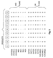
- the truth table of the machine of Fig. 2 is shown in Fig. 3.
- the states of the machine are coded by the variable STATE(0), STATE(1) e STATE(2) which represent the least significative bit, the intermediate bit and the most significative bit of the group of three bits that individuate a certain current state.
- the variables FUTURE(0), FUTURE(1) and FUTURE(2) represent the least significative bit, the intermediate bit and the most significative bit, respectively, of the group of three bits that individuate a future state reached as a result of a certain transition.
- the variables OUT(.) e IN(.) represent the bits of the logic input and output logic signals of the machine corresponding to a certain transition.
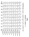
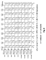
- FIG. 5 A hardware embodiment by the use of a programmable logic array (PLA) of the truth table of Fig. 3 is shown in Figures 5 and 6.
- the considered PLA is built according to an AND-OR pre-charge and valuation scheme.
- the combinatory circuitry, COMBINATORIAL LOGIC, that implements it has 7 inputs, 9 minterms and 8 outputs.
- the AND plane of the PLA of Fig. 5 is constituted by an array of transistors ordered in rows and columns.
- the transistors of a same column are connected in series through their respective current terminals, whereas the control terminals of the transistors belonging to the same row are connected in parallel.
- the top row of the array serves to drive the start-up of the processing, whereas the bottom row serves to extract the computed values once the processing is completed.
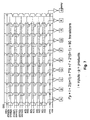
- the OR plane of the PLA shown in Fig. 6, is instead constituted by an array of transistors organized in row and columns which carry out the logic sum of the input minterms and by an output buffer.
- the transistors that belong to the same column of the array have their control terminals connected to a respective control line coupled to a certain minterm, a first current terminal connected to a reference potential, and the transistors of a same row have their second current terminal either connected or not to a respective output line.
- the output buffer which in the cited figure appears on the left hand side, is constituted by a column of inverters each of which is connected to a respective output line and to a respective enabling transistor connected between the respective output line and the supply voltage VDD.
- the PLA is a pre-charge and evaluation circuit, that is, the internal nodes are first pre-charged and then discharged during the evaluation phase if the input pattern corresponds to the expected one.
- the PLA is provided with a dummy path (DUMMY), as depicted in Figures 5 and 6, designed to be the slowest of all.
- This path (DUMMY) is constituted by a set of as many transistors as the number of independent logic variables needed to realize the machine.
- the dummy path Because the dummy path has the largest number of transistors amongst the various paths of the PLA, it will consequently be also the slowest to reach a steady state of operation. Therefore, when a signal propagates through all the dummy path's transistors, surely all the other input signals will have propagated through their respective paths and thereby the evaluation phase may be completed.
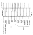
- FIG. 4 A possible temporal diagram of the signals relative to the logic variables of the table of Figure 3 relative to the "E" transition is shown in Fig. 4.
- the pre-charge phases of the AND (CPPA) and OR (CPPO) plane are active low and are out-phased among them so that the output of the AND plane of the PLA may have reached a steady state before the start of the processing carried out by the OR plane of the PLA.
- the variables STATE(.) and IN(.) assume their respective values.
- the outputs OUT(.) and FUTURE(.) assume their respective final values, which are read only when the DUMMY path reaches a steady state and has delivered an OUTDUMMY output signal.
- a combinatorial network having an "i" number of input variables may be realized with a PLA with 2 * I inputs, that is, the "i" input variables plus their respective inverted logic signal. This occurs because in order to ensure the programmability of the PLA the input variables and the respective inverted logic signals should be available.
- All these transistors may have minimum dimensions because they are designed for a specific requirement in a restricted area, therefore with a small parasite load.
- the reprogramming process is realized by modifying the connection of only one terminal of the transistors of the AND plane and of the OR plane.
- the gate of the transistors is depicted in correspondence of the true signal ("1" in the truth table) and of the inverted signal ("0" in the truth table), while it is not shown at all in correspondence of "don't cares" ("-" in the truth table).
- the transistors are depicted omitting some of the contacts that connect them to the output line.
- the contacts are either shown if the output is conditioned by the minterm considered ("1" in the truth table) or not if the minterm does not concur to the output line ("0" in the truth table).
- a reprogramming of the entire algorithm may be implemented by establishing or not certain connections using poly gate and contact masks.
- the AND plane requires a silicon area of 2*i*p transistors for the logic content of the plane.
- a silicon area of i*p transistors should be theoretically sufficient to realize any minterm. Therefore, there exists a silicon area reserved to i*p transistors that remains always unused.
- a second drawback relates to the fact that the drain nodes of the unused transistors of the OR plane remain floating, a condition that should be avoided in VLSI circuits.
- a third problems relates to the requisite of two distinct masks to reprogram this type of PLA, one mask for the AND plane and another one for the OR plane, while it would be certainly more cost effective to use the same mask for both planes.
- the dummy path serves solely to know when to read the PLA outputs, because the different paths are characterized by different signal propagation times.
- the CMOS logic programmable array (PLA) of the invention has at least an AND plane comprising an array of transistors arranged in rows and columns.
- the transistors belonging to a same column are electrically in series and the opposite end current terminals of the series of transistors are coupled to a supply voltage (VDD) and to a reference potential (GND), respectively, and the transistors of the first row and of the last row of the array have their control terminals connected to respective enabling potentials.
- each other row of the array is associated to three different control lines.
- a first line is coupled to a first input value
- the second line is coupled to the logic inverted value of the first input value
- the third line is coupled to a potential that maintains in a state of conduction the transistors connected to it, each transistor of each non-extreme row has its control terminal connected to one of the three control lines.
- the AND plane of the PLA of the invention may have a column (DUMMY) of transistors the control terminals which with the exception of the transistors belonging to the two extreme rows are coupled to a voltage that maintains them in a conduction state.
- DUMMY column of transistors the control terminals which with the exception of the transistors belonging to the two extreme rows are coupled to a voltage that maintains them in a conduction state.
- a logic programmable array may have at least an OR plane comprising an array of transistors arranged in rows and columns.
- the transistors belonging to a same column have their control terminals connected to a respective control line and a first current terminal coupled to a reference voltage (GND), each transistor of each row of the array having a second current terminal connected or not to a respective output line, and those not connected to a respective output line are short-circuited to the respective first current terminal.
- GND reference voltage
- the OR plane of the PLA may optionally have a column (DUMMY) of transistors whose control terminals are connected to a respective control line while the current terminals are coupled to the reference potential (GND).
- DUMMY column of transistors whose control terminals are connected to a respective control line while the current terminals are coupled to the reference potential (GND).
- a PLA containing at least an AND plane can be made with a reduced silicon area requisite.
- the AND plane of a PLA of the invention instead of having a transistor on an input line or on the inverted input line, or no transistor at all, there is a unique transistor whose gate is either connected to the input line or to the inverted input line, or to the supply node (in which case the transistor is kept in a conduction state), as highlighted in Fig. 7.
- the AND plane requires a silicon area of integration sufficient for:
- the logic content requires a silicon area for i*p transistors rather than 2*i*p transistors as in the PLAs of the prior art. Therefore, for the same area occupied by each transistor, and for implementing a certain Boolean function, the PLA of the invention, occupies less space than a known PLA.
- a further advantage is that each column of the AND plane counts the same number of transistors in series, and thereby each minterm requires the same time to be valuated. This guarantees that all the outputs reach their final value practically at the same instant. This may even permit (if so desired) to realize a simple and convenient external timing instead of a more burdensome DUMMY path.
- a PLA realized with such an AND plane may be reprogrammed through the first metalization level.
- the plane AND also the OR plane may also be reprogrammed through the first metalization level and therefore the PLA of the invention may be reprogrammed with only one mask.
- pre-charge and valuation PLAs may be realized with a single AND plane.
- the new PLA occupies undoubtedly less space than known PLAs for the same combinatorial logic.
- the performances of a PLA of the invention are better than those of a PLA. Indeed, in known PLAs the timing is based on a DUMMY path, that is the slowest of all internal paths.
- the DUMMY path is realized by connecting all the transistors of a column of the AND plane in series and by eventually using only one transistor of the OR plane if present (with all the others acting as a parasite load).
- the PLA of the invention surely "decides" within the time delay set by an eventual DUMMY path.
- the PLA of the invention decides in a shorter time delay than known PLAs, because the length of the columns of the AND plane is practically halved by virtue of the fact that the number of the parasite transistors is halved (i*p rather than 2*i*p) and so is the load. Therefore, the valuation of the minterms is faster and the overall decision time is shorter.
- the valuation time of the AND plane is uniform, that it is equal for all the minterms, because each minterm sees the same number of transistors in series toward the power supply rail.
- the spread of the valuation time of the OR plane if present, is contained. This makes possible the realization of a PLA even without any DUMMY path, that is, by using as pre-charge and valuation commands, signals purposely generated, linked to the clock that drives the PLA itself.
Description
- 2*i*p transistors for the content;
- 2*i transistors for the DUMMY PATH;
- 2*(p+1) for the pre-charge of the minterms;
- p inverters.
- o*p transistors for the content;
- o+p+1 transistors for the DUMMY PATH;
- o+1 for the pre-charge of the minterms;
- o+1 inverters.
- i*p transistors for the content.
- 2*i transistors for the DUMMY path.
- 2*(p+1) for the pre-charge of the minterms
- p inverters.
Claims (2)
- A CMOS programmable logic array (PLA) having at least an AND plane comprising an array of transistors arranged in rows and columns, the transistors belonging to a same column being connected in series with each other, the two end current terminals of said series of transistors being coupled to the supply voltage rail (VDD) and to a reference (GND), respectively, to each row of said array with the exception of the first and the last rows are associated a first control line coupled to a first input value, a second control line coupled to the inverted logic value of said first input value and a third control line, characterized in that
said third control line is coupled to a voltage sufficient to keep in a state of conduction all the transistors of the row having their gate electrode connected to it;
each transistor of each row except said first and said last row has its control terminal connected to one of said three control lines associated to the row.
the transistors of the first row and of the last row of the array having their control terminals coupled to respective opposite enabling/disabling potentials (CCPA). - The programmable logic array (PLA) of claim 1, further comprising a column (DUMMY) of transistors, wherein the control terminals of the transistors belonging to all the rows except the first row and the last row are coupled to said third line.
Priority Applications (3)
| Application Number | Priority Date | Filing Date | Title |
|---|---|---|---|
| DE60015916T DE60015916D1 (en) | 2000-02-14 | 2000-02-14 | Programmable logical fields |
| EP00830102A EP1126614B1 (en) | 2000-02-14 | 2000-02-14 | Programmable logic arrays |
| US09/782,173 US6396168B2 (en) | 2000-02-14 | 2001-02-12 | Programmable logic arrays |
Applications Claiming Priority (1)
| Application Number | Priority Date | Filing Date | Title |
|---|---|---|---|
| EP00830102A EP1126614B1 (en) | 2000-02-14 | 2000-02-14 | Programmable logic arrays |
Publications (2)
| Publication Number | Publication Date |
|---|---|
| EP1126614A1 EP1126614A1 (en) | 2001-08-22 |
| EP1126614B1 true EP1126614B1 (en) | 2004-11-17 |
Family
ID=8175181
Family Applications (1)
| Application Number | Title | Priority Date | Filing Date |
|---|---|---|---|
| EP00830102A Expired - Lifetime EP1126614B1 (en) | 2000-02-14 | 2000-02-14 | Programmable logic arrays |
Country Status (3)
| Country | Link |
|---|---|
| US (1) | US6396168B2 (en) |
| EP (1) | EP1126614B1 (en) |
| DE (1) | DE60015916D1 (en) |
Families Citing this family (8)
| Publication number | Priority date | Publication date | Assignee | Title |
|---|---|---|---|---|
| US7170315B2 (en) | 2003-07-31 | 2007-01-30 | Actel Corporation | Programmable system on a chip |
| US7521960B2 (en) | 2003-07-31 | 2009-04-21 | Actel Corporation | Integrated circuit including programmable logic and external-device chip-enable override control |
| US7138824B1 (en) * | 2004-05-10 | 2006-11-21 | Actel Corporation | Integrated multi-function analog circuit including voltage, current, and temperature monitor and gate-driver circuit blocks |
| US7099189B1 (en) | 2004-10-05 | 2006-08-29 | Actel Corporation | SRAM cell controlled by non-volatile memory cell |
| US7116181B2 (en) * | 2004-12-21 | 2006-10-03 | Actel Corporation | Voltage- and temperature-compensated RC oscillator circuit |
| US7119398B1 (en) * | 2004-12-22 | 2006-10-10 | Actel Corporation | Power-up and power-down circuit for system-on-a-chip integrated circuit |
| US7446378B2 (en) * | 2004-12-29 | 2008-11-04 | Actel Corporation | ESD protection structure for I/O pad subject to both positive and negative voltages |
| DE202014009180U1 (en) | 2014-11-14 | 2015-01-14 | Technische Universität Ilmenau | Pressure gradient-controlled lamellar valve with adjustable stiffness |
Family Cites Families (7)
| Publication number | Priority date | Publication date | Assignee | Title |
|---|---|---|---|---|
| US4142176A (en) * | 1976-09-27 | 1979-02-27 | Mostek Corporation | Series read only memory structure |
| KR920011006B1 (en) * | 1983-08-22 | 1992-12-26 | 가부시끼가이샤 히다찌세이사꾸쇼 | Semiconductor integrated circuit device |
| JPS6169215A (en) * | 1984-09-12 | 1986-04-09 | Nec Corp | Programmable logic array |
| US4697105A (en) * | 1986-07-23 | 1987-09-29 | American Telephone And Telegraph Company, At&T Bell Laboratories | CMOS programmable logic array |
| US4760290A (en) * | 1987-05-21 | 1988-07-26 | Vlsi Technology, Inc. | Synchronous logic array circuit with dummy signal lines for controlling "AND" array output |
| JP2575899B2 (en) * | 1989-10-26 | 1997-01-29 | 株式会社東芝 | Precharge type logic circuit |
| US6137318A (en) * | 1997-12-09 | 2000-10-24 | Oki Electric Industry Co., Ltd. | Logic circuit having dummy MOS transistor |
-
2000
- 2000-02-14 DE DE60015916T patent/DE60015916D1/en not_active Expired - Lifetime
- 2000-02-14 EP EP00830102A patent/EP1126614B1/en not_active Expired - Lifetime
-
2001
- 2001-02-12 US US09/782,173 patent/US6396168B2/en not_active Expired - Lifetime
Also Published As
| Publication number | Publication date |
|---|---|
| US20010030554A1 (en) | 2001-10-18 |
| EP1126614A1 (en) | 2001-08-22 |
| US6396168B2 (en) | 2002-05-28 |
| DE60015916D1 (en) | 2004-12-23 |
Similar Documents
| Publication | Publication Date | Title |
|---|---|---|
| US5808479A (en) | High speed programmable logic architecture | |
| US5081375A (en) | Method for operating a multiple page programmable logic device | |
| US5894228A (en) | Tristate structures for programmable logic devices | |
| US6208163B1 (en) | FPGA configurable logic block with multi-purpose logic/memory circuit | |
| US9048833B2 (en) | Storage elements for a configurable IC and method and apparatus for accessing data stored in the storage elements | |
| US7545167B2 (en) | Configurable IC with interconnect circuits that also perform storage operations | |
| US6069490A (en) | Routing architecture using a direct connect routing mesh | |
| US7656188B2 (en) | Reconfigurable IC that has sections running at different reconfiguration rates | |
| US5016217A (en) | Logic cell array using CMOS EPROM cells having reduced chip surface area | |
| US7420389B2 (en) | Clock distribution in a configurable IC | |
| US6882177B1 (en) | Tristate structures for programmable logic devices | |
| US20040225980A1 (en) | Architecture for a connection block in reconfigurable gate arrays | |
| EP0379071B1 (en) | Multiple page programmable logic architecture | |
| GB2304436A (en) | Nonvolatile programmable memory cells and cell arrays | |
| US5614844A (en) | High speed programmable logic architecture | |
| US5319261A (en) | Reprogrammable interconnect architecture using fewer storage cells than switches | |
| US7932745B2 (en) | Inverting flip-flop for use in field programmable gate arrays | |
| EP1126614B1 (en) | Programmable logic arrays | |
| KR100214195B1 (en) | Gate array capable of field programming and the method | |
| EP0573637B1 (en) | Eprom-based crossbar switch with zero standby power | |
| US7285981B2 (en) | Configuration circuit for programmable logic devices | |
| US5465055A (en) | RAM-logic tile for field programmable gate arrays | |
| US5021689A (en) | Multiple page programmable logic architecture | |
| US5324998A (en) | Zero power reprogrammable flash cell for a programmable logic device | |
| US6269020B1 (en) | FIFO configuration cell |
Legal Events
| Date | Code | Title | Description |
|---|---|---|---|
| PUAI | Public reference made under article 153(3) epc to a published international application that has entered the european phase |
Free format text: ORIGINAL CODE: 0009012 |
|
| AK | Designated contracting states |
Kind code of ref document: A1 Designated state(s): DE FR GB IT Kind code of ref document: A1 Designated state(s): AT BE CH CY DE DK ES FI FR GB GR IE IT LI LU MC NL PT SE |
|
| AX | Request for extension of the european patent |
Free format text: AL;LT;LV;MK;RO;SI |
|
| 17P | Request for examination filed |
Effective date: 20020115 |
|
| AKX | Designation fees paid |
Free format text: DE FR GB IT |
|
| 17Q | First examination report despatched |
Effective date: 20020503 |
|
| GRAP | Despatch of communication of intention to grant a patent |
Free format text: ORIGINAL CODE: EPIDOSNIGR1 |
|
| GRAS | Grant fee paid |
Free format text: ORIGINAL CODE: EPIDOSNIGR3 |
|
| GRAA | (expected) grant |
Free format text: ORIGINAL CODE: 0009210 |
|
| AK | Designated contracting states |
Kind code of ref document: B1 Designated state(s): DE FR GB IT |
|
| REG | Reference to a national code |
Ref country code: GB Ref legal event code: FG4D |
|
| RIN1 | Information on inventor provided before grant (corrected) |
Inventor name: FERRARIO, DONATO Inventor name: YERO, EMILIO Inventor name: CAMPARDO, GIOVANNI Inventor name: GHEZZI, STEFANO |
|
| REF | Corresponds to: |
Ref document number: 60015916 Country of ref document: DE Date of ref document: 20041223 Kind code of ref document: P |
|
| PG25 | Lapsed in a contracting state [announced via postgrant information from national office to epo] |
Ref country code: DE Free format text: LAPSE BECAUSE OF FAILURE TO SUBMIT A TRANSLATION OF THE DESCRIPTION OR TO PAY THE FEE WITHIN THE PRESCRIBED TIME-LIMIT Effective date: 20050218 |
|
| PLBE | No opposition filed within time limit |
Free format text: ORIGINAL CODE: 0009261 |
|
| STAA | Information on the status of an ep patent application or granted ep patent |
Free format text: STATUS: NO OPPOSITION FILED WITHIN TIME LIMIT |
|
| 26N | No opposition filed |
Effective date: 20050818 |
|
| ET | Fr: translation filed | ||
| PGFP | Annual fee paid to national office [announced via postgrant information from national office to epo] |
Ref country code: GB Payment date: 20070130 Year of fee payment: 8 |
|
| PGFP | Annual fee paid to national office [announced via postgrant information from national office to epo] |
Ref country code: IT Payment date: 20070607 Year of fee payment: 8 |
|
| PGFP | Annual fee paid to national office [announced via postgrant information from national office to epo] |
Ref country code: FR Payment date: 20070227 Year of fee payment: 8 |
|
| GBPC | Gb: european patent ceased through non-payment of renewal fee |
Effective date: 20080214 |
|
| REG | Reference to a national code |
Ref country code: FR Ref legal event code: ST Effective date: 20081031 |
|
| PG25 | Lapsed in a contracting state [announced via postgrant information from national office to epo] |
Ref country code: FR Free format text: LAPSE BECAUSE OF NON-PAYMENT OF DUE FEES Effective date: 20080229 |
|
| PG25 | Lapsed in a contracting state [announced via postgrant information from national office to epo] |
Ref country code: GB Free format text: LAPSE BECAUSE OF NON-PAYMENT OF DUE FEES Effective date: 20080214 |
|
| PG25 | Lapsed in a contracting state [announced via postgrant information from national office to epo] |
Ref country code: IT Free format text: LAPSE BECAUSE OF NON-PAYMENT OF DUE FEES Effective date: 20080214 |