EP1134837A1 - Antenna device for high frequency radio, high frequency radio apparatus and watch type radio apparatus - Google Patents
Antenna device for high frequency radio, high frequency radio apparatus and watch type radio apparatus Download PDFInfo
- Publication number
- EP1134837A1 EP1134837A1 EP00962947A EP00962947A EP1134837A1 EP 1134837 A1 EP1134837 A1 EP 1134837A1 EP 00962947 A EP00962947 A EP 00962947A EP 00962947 A EP00962947 A EP 00962947A EP 1134837 A1 EP1134837 A1 EP 1134837A1
- Authority
- EP
- European Patent Office
- Prior art keywords
- antenna
- radio apparatus
- frequency radio
- antenna element
- antenna device
- Prior art date
- Legal status (The legal status is an assumption and is not a legal conclusion. Google has not performed a legal analysis and makes no representation as to the accuracy of the status listed.)
- Ceased
Links
Images


Classifications
-
- G—PHYSICS
- G04—HOROLOGY
- G04B—MECHANICALLY-DRIVEN CLOCKS OR WATCHES; MECHANICAL PARTS OF CLOCKS OR WATCHES IN GENERAL; TIME PIECES USING THE POSITION OF THE SUN, MOON OR STARS
- G04B47/00—Time-pieces combined with other articles which do not interfere with the running or the time-keeping of the time-piece
-
- H—ELECTRICITY
- H01—ELECTRIC ELEMENTS
- H01Q—ANTENNAS, i.e. RADIO AERIALS
- H01Q1/00—Details of, or arrangements associated with, antennas
- H01Q1/27—Adaptation for use in or on movable bodies
- H01Q1/273—Adaptation for carrying or wearing by persons or animals
-
- H—ELECTRICITY
- H01—ELECTRIC ELEMENTS
- H01Q—ANTENNAS, i.e. RADIO AERIALS
- H01Q1/00—Details of, or arrangements associated with, antennas
- H01Q1/48—Earthing means; Earth screens; Counterpoises
-
- H—ELECTRICITY
- H01—ELECTRIC ELEMENTS
- H01Q—ANTENNAS, i.e. RADIO AERIALS
- H01Q13/00—Waveguide horns or mouths; Slot antennas; Leaky-waveguide antennas; Equivalent structures causing radiation along the transmission path of a guided wave
- H01Q13/08—Radiating ends of two-conductor microwave transmission lines, e.g. of coaxial lines, of microstrip lines
-
- H—ELECTRICITY
- H01—ELECTRIC ELEMENTS
- H01Q—ANTENNAS, i.e. RADIO AERIALS
- H01Q9/00—Electrically-short antennas having dimensions not more than twice the operating wavelength and consisting of conductive active radiating elements
- H01Q9/04—Resonant antennas
- H01Q9/0407—Substantially flat resonant element parallel to ground plane, e.g. patch antenna
- H01Q9/0421—Substantially flat resonant element parallel to ground plane, e.g. patch antenna with a shorting wall or a shorting pin at one end of the element
-
- H—ELECTRICITY
- H04—ELECTRIC COMMUNICATION TECHNIQUE
- H04B—TRANSMISSION
- H04B1/00—Details of transmission systems, not covered by a single one of groups H04B3/00 - H04B13/00; Details of transmission systems not characterised by the medium used for transmission
- H04B1/38—Transceivers, i.e. devices in which transmitter and receiver form a structural unit and in which at least one part is used for functions of transmitting and receiving
- H04B1/3827—Portable transceivers
- H04B1/385—Transceivers carried on the body, e.g. in helmets
Definitions
- the present invention relates to an antenna device used in high-frequency radio apparatuses and a compact-size high-frequency radio apparatus which uses the antenna device, and in particular, to a very compact-size high-frequency radio apparatus such as a watch-shaped high-frequency radio apparatus and an antenna device used in high-frequency radio apparatuses.
- a helical dipole antenna is generally used as an antenna for portable devices such as cellular phones which belongs to high-frequency radio apparatuses.
- the helical dipole antenna is configured in a manner that it is drawn out from or kept contained into the case of a portable device when used.
- a thin card type portable apparatus for 2.4[GHz] band employs a chip antenna using ceramic material.
- the degree of freedom for arrangement is low in the inverted-F antenna, since both its antenna element and its ground plate (main plate) are formed as an integral unit. As a result, the inverted-F antenna is difficult to be made compact any more.
- the chip antenna although the chip antenna itself can be surface-mounted, an antenna including its peripheral circuit is still large as a part. In addition, the chip antenna is fairly high in cost.
- An object of the present invention is therefore to provide an antenna device for a high-frequency radio apparatus, a high-frequency radio apparatus, and a watch-shaped radio apparatus, which can be made more compact, increase sensitivity of the apparatus, and be prevented from being damaged by static electricity.
- a first aspect of the present invention is characterized in that an antenna device for a high-frequency radio apparatus connected to both an earth pattern and a feeding point formed on a circuit substrate, comprising: a metal-made antenna element whose one end is connected to the earth pattern and folded in an L-shape in section; and a feeding line whose one end is connected to the feeding point and whose other end is electrically fixedly connected to a position on the antenna element, the position being corresponding to a predetermined value of impedance of the antenna device for the high-frequency radio apparatus.
- a second aspect of the present invention is characterized in that, in the first aspect of the present invention, an orthogonal projection of the antenna element which is made onto the earth pattern serving as a surface of projection is included in the earth pattern.
- a third aspect of the present invention is characterized in that, in the first aspect of the present invention, an orthogonal projection of the antenna element which is made onto the earth pattern serving as a surface of projection is smaller in area than the earth pattern.
- a fourth aspect of the present invention is characterized in that, in the first aspect of the present invention, the antenna element is shaped into a lead wire.
- a fifth aspect of the present invention is characterized in that, in the first aspect of the present invention, a dielectric member is arranged in the vicinity of the antenna element so as to set a resonance frequency of the antenna device for the high-frequency radio apparatus to a predetermined resonance frequency.
- a sixth aspect of the present invention is characterized in that, in the fifth aspect of the present invention, a dielectric constant of the dielectric member is set in accord with the resonance frequency.
- a seventh aspect of the present invention is characterized in that, in the fifth aspect of the present invention, the dielectric member is arranged closely to the antenna element and a closely arranged state of the dielectric member is determined in accord with the resonance frequency.
- An eighth aspect of the present invention is characterized in that, in the fifth aspect of the present invention, a dielectric member for securing a display device,a substrate, a battery, or other components is arranged in the vicinity of the antenna element.
- a ninth aspect of the present invention is characterized in that, in the first aspect of the present invention, length of the antenna element is set to length of approximately a quarter of a wavelength of frequency to be used.
- a tenth aspect of the present invention is characterized in that the high-frequency radio apparatus having the antenna device according to the first aspect of the present invention, comprising: a circuit substrate on which various electrical circuits are mounted; and a display device for displaying various pieces of information, the display device being arranged in a space to one side of the circuit substrate, wherein the antenna device is arranged on the side of the display device of the circuit substrate.
- An eleventh aspect of the present invention is characterized in that, in the tenth aspect of the present invention, comprising: a case body containing the antenna device, the display device, and the circuit substrate; a case back, made of conductive material, constituting a case together with the case body; and a battery for supplying power to drive the high-frequency radio apparatus, wherein the case back is conductibly connected to either an earth potential of the circuit substrate or one electrode of the battery connected in AC (alternating current) to the earth potential.
- An twelfth aspect of the present invention is characterized in that, an antenna device for a high-frequency radio apparatus connected to both an earth pattern and a feeding point formed over an approximately overall area of at least any one layer of plural layers included in a multilayer circuit substrate, comprising: a metal-made antenna element whose one end is connected to the earth pattern and folded in an L-shape in section; and a feeding line whose one end is connected to the feeding point and whose other end is electrically fixedly connected to a position on the antenna element, the position corresponding to a predetermined value of impedance of the antenna device for the high-frequency radio apparatus.
- a thirteenth aspect of the present invention is characterized in that, in the twelfth aspect of the present invention, an orthogonal projection of the antenna element which is made onto the earth pattern serving as a surface of projection is included in the earth pattern.
- a fourteenth aspect of the present invention is characterized in that, in the twelfth aspect of the present invention, an orthogonal projection of the antenna element which is made onto the earth pattern serving as a surface of projection is smaller in area than the earth pattern.
- a fifteenth aspect of the present invention is characterized in that, in the twelfth aspect of the present invention, the antenna element is shaped into a lead wire.
- a sixteenth aspect of the present invention is characterized in that, in the twelfth aspect of the present invention, a dielectric member is arranged in the vicinity of the antenna element so as to set a resonance frequency of the antenna device for the high-frequency radio apparatus to a predetermined resonance frequency.
- a seventeenth aspect of the present invention is characterized in that, in the sixteenth aspect of the present invention, a dielectric constant of the dielectric member is set in accord with the resonance frequency.
- An eighteenth aspect of the present invention is characterized in that, in the sixteenth aspect of the present invention, the dielectric member is arranged closely to the antenna element and a closely arranged state of the dielectric member is determined in accord with the resonance frequency.
- a nineteenth aspect of the present invention is characterized in that, in the twelfth aspect of the present invention, the dielectric member is configured so as to secure a display device, substrate, a battery, and other components.
- a twentieth aspect of the present invention is characterized in that, in the twelfth aspect of the present invention, length of the antenna element is set to length of approximately a quarter of a wavelength of frequency to be used.
- a twenty-first aspect of the present invention is characterized in that the high-frequency radio apparatus having the antenna device according to the twenty aspect of the present invention, comprising: a circuit substrate on which various electrical circuits are mounted; and a display device for displaying various pieces of information, the display device being arranged in a space to one side of the circuit substrate, wherein the antenna device is arranged on the side of the display device of the circuit substrate.
- a twenty-second aspect of the present invention is characterized in that, in the twenty-first aspect of the present invention, comprising: a case body containing the antenna device, the display device, and the circuit substrate; a case back, made of conductive material, constituting a case together with the case body; and a battery for supplying power to drive the high-frequency radio apparatus, wherein the case back is conductibly connected to either an earth potential of the circuit substrate or one electrode of the battery connected in AC (alternating current) to the earth potential.
- a twenty-third aspect of the present invention is characterized in that, an antenna device for a high-frequency radio apparatus connected to both an earth pattern and a feeding point formed on a circuit substrate, comprising: a metal-made antenna element whose one end is connected to the earth pattern and folded in an L-shape in section; and a feeding line whose one end is connected to the feeding point and whose other end is fixedly connected to the earth pattern.
- a twenty-fourth aspect of the present invention is characterized in that, in the twenty-third aspect of the present invention, the earth pattern is composed of an electrode pattern formed on the circuit substrate.
- a twenty-fifth aspect of the present invention is characterized in that, in the twenty-fourth aspect of the present invention, the earth pattern is formed over an approximately overall range of a surface positioned under the antenna element.
- a twenty-sixth aspect of the present invention is characterized in that, in the twenty-third aspect of the present invention, length of the antenna element is set to length of approximately a quarter of a wavelength of frequency to be used.
- a twenty-seventh aspect of the present invention is characterized in that, comprising: a wristwatch-shaped case; an antenna device for a high-frequency radio apparatus defined by the twenty-third aspect of the present invention, wherein the antenna device for the high-frequency radio apparatus is arranged within the wristwatch-shaped case.
- a twenty-eighth aspect of the present invention is characterized in that, comprising: a case; a substrate having an earth pattern and being arranged within the case; an antenna element whose one end is electrically connected to the earth pattern, the antenna element being arranged three-dimensionally to the circuit substrate, and partially arranged on an upper surface of the case; and a feeding line whose one end is connected to the earth pattern, whose other end is connected to a feeding point, and the feeding line being arranged three-dimensionally to the circuit substrate in parallel to a direction connecting one end side and the other end side of the antenna element.
- a twenty-ninth aspect of the present invention is characterized in that, in the twenty-eight aspect of the present invention, the antenna element is made of metal material and connected to the earth pattern via a conductive member, the conductive member is made of the same metal material as that of the antenna element, and both the antenna element and the conductive member are integrally formed in an L-shape.
- a thirtieth aspect of the present invention is characterized in that, an antenna device for a high-frequency radio apparatus according to the twenty-eighth aspect of the present invention; a circuit substrate on which a radio circuit is formed, the radio circuit being connected to the antenna device for the high-frequency radio apparatus; and a wristwatch-shaped case containing both the antenna device for the high-frequency radio apparatus and the circuit substrate.
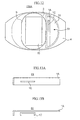
- Fig.1 shows a schematic sectional view of a watch-shaped radio apparatus according to a first embodiment.
- Fig.2 shows a schematic perspective view of the top of the watch-shaped radio apparatus according to the first embodiment.
- Fig.3A is a plan view showing an inverted-F antenna of the first embodiment.
- Fig.3B is a front view showing the inverted-F antenna of the first embodiment.
- Fig.4A is a plan view showing an inverted-F antenna of a second embodiment.
- Fig.4B is a front view showing the inverted-F antenna of the second embodiment.
- Fig.5 illustrates a mounted state of the inverted-F antenna.
- Fig.6 is a cross sectional view showing the part of an antenna of the watch-shaped radio apparatus in order to exemplify a retaining mechanism.
- Fig.7 is an illustration of another example of the retaining mechanism.
- Fig.8 is an illustration of an example for forming a ground pattern on a multilayer substrate.
- Fig.9 shows a cross section of the multilayer substrate in Fig.8.
- Fig.10 illustrates an example of a characteristic of the inverted-F antenna.
- Fig.11 shows a schematic sectional view of a watch-shaped radio apparatus according to a third embodiment.
- Fig.12 shows a schematic perspective view from the top of the watch-shaped radio apparatus.
- Fig.13A is a plan view showing an inverted-L antenna of the third embodiment.
- Fig.13B is a front view showing the inverted-L antenna of the third embodiment.
- Fig.14A is a plan view showing a mounted inverted-L antenna of a fourth embodiment.
- Fig.14B is a front view showing the mounted inverted-L antenna of the fourth embodiment.
- Fig.15 illustrates a mounted state of the inverted-L antenna.
- Fig.16A is a plan view showing an inverted-L antenna according to a fifth embodiment.
- Fig.16B is a front view showing the inverted-L antenna according to the fifth embodiment.
- Fig.17A is a plan view showing the mounted inverted-L antenna of the fifth embodiment.
- Fig.17B is a front view showing the mounted inverted-L antenna of the fifth embodiment.
- Fig.18 illustrates an example of a characteristic of the inverted-L antenna.
- Fig.19 illustrates a mounted state of the inverted-L antenna according to the fifth embodiment.
- Fig.20 is a sectional view showing a watch-shaped radio apparatus of a sixth embodiment.
- Fig.21 is a schematic perspective view from the top of the watch-shaped radio apparatus according to the sixth embodiment.
- Fig.22A is an outer oblique view (part 1) of a case on which an antenna element is secured.
- Fig.22B is an outer oblique view (part 2) of a case on which an antenna element is secured.
- Fig.23 illustrates a first modification of the embodiments.
- Fig.24A is an outer oblique view (part 1) of an antenna unit according to a second modification.
- Fig.24B is a sectional view (part 1) of the antenna unit according to the second modification.
- Fig.25A is an outer oblique view (part 2) of the antenna unit according to the second modification.
- Fig.25B is a sectional view (part 2) of the antenna unit according to the second modification.
- Fig. 1 is a schematic sectional view of a watch-shaped radio apparatus according to a first embodiment of the present invention.
- an inverted-F antenna 1 which is formed three-dimensionally and incorporated in a watch-shaped radio apparatus 100 as an antenna device for a high-frequency radio apparatus.
- the inverted-F antenna 1 comprises an antenna element 1A and a feeding line 1B.
- the antenna element 1A is made of metal and formed into an L-shape in section.
- the antenna element 1A is fixedly connected to a ground pattern (earth pattern) mounted on a circuit substrate 2. Soldering is a normal way to connect the antenna element 1A to the circuit substrate 2.
- the feeding line 1B is conductibly secured at a given position on the antenna element 1A.
- the circuit substrate 2 of the watch-shaped radio apparatus 100 is sandwiched from its upper and lower sides by plastic members 3 and 5.
- a micro nut 13 is inserted and formed in advance.
- the circuit substrate 2 is secured by applying a micro screw 14 to the micro nut 13 through the plastic member 5 from under the plastic member 3.
- An electric circuit 8 is mounted on the lower surface of the circuit substrate 2 and includes a radio circuit consisting of electric parts.
- the electric circuit 8 is illustrated as a rectangular module for the sake of simplifying the drawing. Instead of such a module, the parts of the electric circuit 8 can be mounted directly on the substrate 2.
- a button type battery 6 is used as a power source of the watch-shaped radio apparatus.
- the button type battery 6, which is secured on the member 5, is electrically connected to a case back 7 via a conductive plate which is not shown.
- a cover glass 9 is fixedly arranged on a watchcase 4.
- the display of the LCD 10 can therefore be seen through the cover glass 9.
- the watchcase 4 and the case back 7 are secured by, usually, screwing.
- Fig. 2 shows a schematic perspective view of the top of the watch-shaped radio apparatus 100.
- a ground pattern 15 is formed on the circuit substrate 2.
- the circuit substrate 2 is not necessarily a rectangular. However in many cases, it may be formed into a curved outer shape or folded-line outer shape. Accordingly, arranging parts and an electrode pattern such as the ground pattern 15 on the circuit substrate 2 in agreement with the shape of the circuit substrate 2 leads to effective utilization of the substrate area for miniaturizing the apparatus.
- Fig. 3A is a plan view of the inverted-F antenna 1 of the first embodiment, while Fig.3B is a front view thereof.
- the inverted-F antenna 1 comprises, as descried above, the plate antenna element 1A folded into an L-shape at one end and the feeding line 1B.
- the antenna element 1A be made of materials, such as copper, whose conductivity is high. It is also possible to use high-conductivity materials as the surface plating.
- the feeding line 1B is conductibly secured at a position on the inverted-F antenna 1A in a way that the inverted-F antenna 1A may have a predetermined value of impedance after its securing.
- the value of impedance is, for example, 50 [ ⁇ ].
- the feeding line 1B is perpendicularly linked to the antenna element 1A.
- antenna element 1A and feeding line 1B be connected to each other by brazing or soldering.
- FIGs. 4A and 4B show a second embodiment of the present invention.
- the same or identical reference numerals as to those in Figs. 1 to 3 are shown with the same reference numerals.
- Fig. 4A is a plan view showing a mounted state of the inverted-F antenna 1 according to the second embodiment.
- Fig. 4B is, on the other hand, is a front view showing the mounted state of the inverted-F antenna 1 of the second embodiment.
- an electric conductor pattern (plane electrodes) 22 is arranged on the upper surface of a circuit substrate 21, on the upper surface of a circuit substrate 21, an electric conductor pattern (plane electrodes) 22 is arranged.
- One end of the antenna element 1A is conductibly secured to the conductor pattern 22.
- the feeding line 1B is conductibly connected to a feeding terminal pattern 23 mounted on the circuit substrate 21.
- a hole pattern as the feeding terminal pattern 23, which is a through hole formed through the circuit substrate 21, and solder the feeding line 23, after inserted into the hole pattern.
- the feeding terminal pattern 23 is linked to the ground (earth) potential in DC (direct current) to a signal supplied from the inverted-F antenna 1.
- Figs. 4A and 4B does not show circuit parts and other structural components structured on the circuit substrate 21, but only show the antenna part.
- the length of the antenna element 1A, which composes the inverted-F antenna 1, is approximately a quarter of a wavelength of a frequency to be used, including its folded portion; for example, approximately 3 [cm] at a frequency of 2.5 [GHz].
- the feeding line 1B is connected to a position on the antenna element 1A so that the position corresponds to a predetermined value of impedance (for example, 50 [ ⁇ ]) to the ground potential in the vicinity of the feeding terminal pattern 23.
- a predetermined value of impedance for example, 50 [ ⁇ ]
- Impedance values of circuit terminals and wiring are determined so that the impedance of signal lines connecting with the feeding terminal pattern 23 from a not-shown circuit is also set to an identical value (for example, 50 [ ⁇ ]).
- the signal lines be formed by strip lines, with a given value of impedance, arranged on the back (not shown) of the circuit substrate 21
- the inverted-F antenna 1 be arranged at the center of the ground pattern of the circuit substrate 21.
- Fig. 5 illustrates a mounted state of the inverted-F antenna.
- a ground pattern 15 is mounted at a position facing the antenna element 1A.
- drive signal electrode patterns 16 are mounted for drive signals to drive the LCD 10.
- Wiring to the LCD 10 of a compact apparatus having an LCD panel is usually realized by connecting drive signal electrodes embedded in the LCD 10 itself and the drive signal electrode patterns 16 mounted on the upper surface of the circuit substrate 21 via the conductive rubber 21 (refer to Fig. 1).
- the LCD 10 that functions as a user interface of the apparatus is arranged at the center thereof.
- the drive signal electrode patterns 16 and a display driver for generating drive signals or a CPU including a display driver, which are not shown, are arranged on the back of the LCD 10.
- the area on the circuit substrate 2, which corresponds to the LCD 10 is occupied by wiring for connecting the drive signal electrode patterns 16 and the CPU.
- a multilayer substrate may be used to arrange such a wiring section on another layer utilizing through holes.
- this method still requires the same substrate area compared to a wiring configuration without a multilayer substrate. This means that utilizing a multilayer substrate does not contribute to the reduction of the area used on the substrate.
- the ground pattern 15 shown in Fig.5 is mounted in some shape, not necessarily rectangular, at one end of the upper surface of the circuit substrate 2.
- the orthogonal projection of the antenna element 1A, whose projected plane is on the ground pattern is included in the ground pattern 15.
- the orthogonal projection of the antenna element 1A, whose projected plane is on the ground pattern is smaller in area than the ground pattern 15.
- a practical example is that, when a frequency to be used is 2.5 [GHz], a length of the antenna element 1A is approximately 28 [mm] in its longitudinal direction and a height from the circuit substrate 2 is 2 [mm]. Under such conditions, the antenna device can be configured to have the antenna element 1A whose width is approximately 2 [mm].
- a thickness of the antenna element 1A can be set to approximately 0.2 [mm].
- the width and thickness of the antenna element are determined to optimum values based on conditions, such as physical strength of material composing the antenna element 1A, spacing allowed on the circuit substrate 2, and a necessary antenna gain.
- the antenna element 1A is made up of urethane-coated copper wire, there are advantages in size, workability, and manufacturing cost.
- Fig. 6 is a sectional view showing only the peripheral part of the antenna element 1A shown in Fig. 1.
- the antenna element 1A positioned over the circuit substrate 2 is retained from the upper side thereof by the plastic member 3 (hatched part) which also functions as a securing frame for the LCD 10. This retainment prevents the antenna element 1A from moving upward from the circuit substrate 2.
- the inverted-F antenna 1 thus constructed has minimal variation in a degree of parallel to the circuit substrate 2 when the antenna is mounted. As a result, variation in the characteristics of the inverted-F antenna 1 can be reduced.
- Fig. 7 illustrates another example of the retaining mechanism.
- the plastic member shown in Fig. 6 is replaced by a plastic member 3B which also loads plastic material beneath the antenna element. If taking the structure into consideration, part of the watchcase may be used as a plastic member having the above function.
- the plastic member 3B retains the antenna element 1A from its upper and lower sides.
- This structure prevents the antenna element 1A from being deformed from its upper and lower sides.
- the wavelength of a frequency to be used is therefore shortened according to a dielectric constant of the dielectric member around the antenna.
- the length of the element that resonates at a desired frequency in the air can adequately be adjusted to a shorter value.
- the above retaining mechanism is able to provide compact antennas, without particular manufacturing process such as a ceramic chip antenna.
- the antenna can be made compact so as to have a practical size, without increasing manufacturing cost unnecessarily.
- a plastic member is generally used as a securing member incorporated within apparatuses including digital watches and compact information devices.
- the securing member is not limited to one made of plastic.
- Various kinds of members made of different dielectric members are usable for shortening the antenna. It is therefore preferable that the securing member be chosen with consideration of excellence in workability, incombustibility, cost, and others.
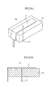
- Fig. 8 is an illustration showing an example of forming the ground pattern for a multilayer substrate.
- Fig. 9 is a sectional view of the multilayer substrate shown in Fig. 8.
- a circuit substrate 2A is a multilayer substrate, in which, as shown in Fig. 9, circuit patterns can be mounted on inner layers as well as its surface.
- a ground pattern 17 is mounted over the almost entire surface of at least one of the inner layer substrates.
- the ground pattern 17 is connected to the ground pattern 15 formed on the front surface of the circuit substrate 2A via a plurality of through holes 18.
- the area of the ground pattern 15 is restricted by the drive signal electrode patterns 16 of the LCD 10, as described before. As shown in Fig.8, the ground pattern 15 is therefore made larger in area than, at least, the orthogonal projection of the antenna element 1A to the ground pattern 15.
- a conductive connection with the ground pattern 17 on inner layers provides a larger ground pattern area.
- the area of the ground pattern 17 on inner layers spread over the almost entire surface on the inner layers.
- the inner substrates are partly used for other wiring patterns.
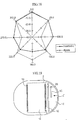
- Fig. 10 exemplifies a radiation pattern of the thus-constructed inverted-F antenna device.
- Fig. 10 exemplifies a radiation pattern of only an inner circuit module excluding the case back 7 (refer to Fig.1). This result reveals that a direction showing a maximum gain is different from that of a dipole antenna, because there is an influence from parts other than the antenna.
- Fig. 1 the case back 7 made of metal such as stainless steel is positioned beneath the watch-shaped radio apparatus according to the embodiments of the present invention.
- the case back 7 is conductibly connected to the positive electrode of the battery 6 by way of terminal plates or others.
- the negative electrode of the battery 6 is electrically connected to the ground pattern of the circuit substrate 2 by way of terminal plates or others.
- the positive electrode of the button type battery 6 is also electrically connected to a power source on the circuit substrate 2 through terminal plates or others.
- a by-pass capacitor is normally electrically connected between a power source terminal and a ground terminal, thereby the circuit being stabilized by a reduced value of impedance of the power source.
- the patterns of the ground and power source are considered to have the same potential in AC (alternating current) to the earth potential.
- the inverted-F antenna 1 is located on the upper side of the apparatus, which is spaced apart from the wrist.
- the ground pattern 15 mounted on the upper surface of the circuit substrate 2A is positioned under the inverted-F antenna 1.
- a ground pattern is positioned on inner layers of the circuit substrate 2A. Further, under the ground pattern formed on the inner layers, the battery 6 and also the case back 7, having a larger area, are positioned.
- the metal-made case back 7 can be regarded as being the same in potential in AC as the ground pattern of the circuit substrate 2A. That is, the metal-made case back 7 has the effect to widen the ground area to the inverted-F antenna 1.
- this wearing results in that the user's body (arm) is connected to the ground potential of the antenna via the case back 7.
- the user's body itself can be considered the ground when the apparatus is worn by a user, thus providing a configuration in which the ground area is further widened to the antenna.
- the apparatus is designed to be worn by a user, a relationship with the human body must be taken into consideration so as to accomplish an optimum antenna operation.
- the antenna is optimized with respect to a relationship with its constituents, and there can be provided a compact radio apparatus whose operating characteristics are stable even when a user wears the apparatus.
- the inverted-F antenna 1 in the first and second embodiments has been constructed three-dimensionally, in which the feeding line should be connected to the antenna perpendicularly.
- This structure causes the distance between the antenna element and the substrate to be longer and the feeding line to be longer. It becomes therefore difficult to realize a given value of the strength of the antenna itself and to hold the antenna in parallel to the ground.
- a third embodiment adopts a feeding line 1C arranged in parallel with the antenna element 1A (refer to Fig. 11).
- Fig. 11 is a schematic sectional view of a watch-shaped radio apparatus according to the third embodiment of the present invention.
- Fig. 11 has the same or identical reference numerals as to those in the first embodiment shown in Fig. 1, which are represented by the same reference numerals.
- an inverted-L antenna 51 is configured three-dimensionally as an antenna device for a high-frequency radio apparatus, which is incorporated in a watch-shaped radio apparatus 100A.
- Fig. 12 shows a schematic perspective view of the top of the watch-shaped radio apparatus 100A.
- a ground pattern 15 is mounted on the circuit substrate 2.
- Fig. 13A is a plan view of the inverted-L antenna 51 of the third embodiment, while the Fig. 13B is a front view thereof.
- the inverted-L antenna 51 comprises, as stated above, a plate-like antenna element 1A whose one end is folded in the L-shape, and a feeding line 1C arranged so as to be in parallel with a longitudinal section of the antenna element 1A at a position spaced apart by a predetermined distance from the antenna element 1A.
- the feeding line 1C is secured at a position that provides a given value of impedance of the inverted-L antenna 51 after being secured.
- the impedance value is 50 [ ⁇ ], for example.
- Figs. 14A and 14B show a fourth embodiment of the present invention.
- the same or identical reference numerals as to those in Figs. 11, 12, 13A or 13B are shown with the same reference numerals.
- Fig. 14A is a plan view showing the mounted-state inverted-L antenna 51 according to the fourth embodiment.
- Fig. 14B is a front view showing the mounted-state inverted-L antenna 51 of the fourth embodiment.
- the electric conductor pattern (plane electrodes) 22 is mounted on the upper surface of the circuit substrate 21, the electric conductor pattern (plane electrodes) 22 is mounted.
- One end of the antenna element 1A is conductibly secured to the conductor pattern 22.
- the feeding line 1C is conductibly connected to a feeding terminal pattern 23 mounted on the circuit substrate 21.
- a hole pattern as the feeding terminal pattern 23, which is a through hole formed through the circuit substrate 21, and solder the feeding line 1B after inserted into the hole pattern.
- the feeding terminal pattern 23 is linked to the ground (earth) potential in DC (direct current) to a signal supplied from the inverted-L antenna 51.
- Figs. 14A and 14B do not show circuit parts and other structural components on the circuit substrate 21, but show only the antenna part.
- the length of the antenna element 1A which composes the inverted-L antenna 51 is approximately a quarter of a wavelength of a frequency to be used, including its folded portion; for example, approximately 3 [cm] at a frequency of 2.5 [GHz].
- the feeding line 1C is connected to a position on the antenna element 1A so that the position corresponds to a predetermined value of impedance (for example, 50 [ ⁇ ]) to the ground potential in the vicinity of the feeding terminal pattern 23.
- a predetermined value of impedance for example, 50 [ ⁇ ]
- Impedance values of circuit terminals and wiring are determined so that the impedance of signal lines connecting with the feeding terminal pattern 23 from a not-shown circuit is also set to an identical value (for example, 50 [ ⁇ ]).
- the signal lines be formed by strip lines, with a given value of impedance, arranged on the back (not shown) of the circuit substrate 21.
- the inverted-L antenna 51 be arranged at the center of the ground pattern of the circuit substrate 21.
- Fig. 15 illustrates a mounted state of the inverted-L antenna.
- a ground pattern 15 is mounted at a position facing the antenna element 1A.
- drive signal electrode patterns 16 is mounted for drive signals to drive the LCD 10.
- Wiring to the LCD 10 of a compact apparatus having an LCD panel is usually realized by connecting drive signal electrodes embedded in the LCD 10 itself and the drive signal electrode patterns 16 mounted on the upper surface of the circuit substrate 2 via the conductive rubber 21 (refer to Fig.1).
- the LCD 10 that functions as a user interface of the apparatus is arranged at the center thereof.
- the drive signal electrode patterns 16 and a display driver for generating drive signals or a CPU including a display driver, which is not shown, are arranged on the back of the LCD 10.
- the area on the circuit substrate 2, which corresponds to the LCD 10 is occupied by wiring for connecting the drive signal electrode patterns 16 and the CPU.
- the ground pattern 15 as shown in Fig.15 is mounted in a shape, not necessarily rectangular, at one end of the upper surface of the circuit substrate 2.
- the orthogonal projection of the antenna element 1A, whose projected plane is on the ground pattern is included in the ground pattern 15.
- the orthogonal projection of the antenna element 1A, whose projected plane is on the ground pattern is smaller in area than the ground pattern 15.
- Figs. 16A and 16B show a fifth embodiment of the present invention.
- the same or identical reference numerals as to those in Figs. 11, 12, 13A or 13B are shown with the same reference numerals.
- an inverted-L antenna 71 comprises an antenna element 1D composed of an L-shaped wire and a feeding line 1C composed of an approximately U-shaped wire.
- the antenna element 1D and the feeding line 1C can easily be formed by, for example, bending wires such as urethane-coated copper wires.
- the feeding line 1C is arranged so that its longitudinal direction becomes parallel with the antenna element 1D, along by a side of the antenna element 1D.
- the feeding line 1C is arranged so that it keeps a proper electric coupling with the antenna element 1D.
- one end of the feeding line 1C is electrically connected with the feeding point 23, while the other end is electrically connected with the ground pattern 22.
- This arrangement permits the impedance observed from the feeding point 23 to be set to a desired value (for example, 50 [ ⁇ ]) at a frequency to be used.
- the gain in a directional range of 135 to 225 degrees may be worse than that of a dipole antenna, the gain in the remaining directional range is better than that of a dipole antenna.
- Fig. 19 shows an example of arranging the antenna on the substrate, when the antenna device described in the fifth embodiment is incorporated into a wristwatch-shaped radio apparatus.
- the feeding line 1C is arranged in parallel with a side of the antenna element 1D of the inverted-L antenna 71, and one end of the feeding line 1C is electrically connected with the feeding point 23, whilst the other end is electrically connected to the ground pattern 15 which is mounted under the antenna element 1D.
- Fig. 19 only a set of the antenna element 1D, feeding line 1C, and LCD drive electrodes 16 are depicted. It is preferable that the antenna element 1D be retained in parallel to the ground pattern 15 with the help of a plastic member or others.
- Fig. 20 is a schematic sectional view showing a watch-shaped radio apparatus of a sixth embodiment
- Fig. 21 is a schematic perspective view from the top thereof.
- the sixth embodiment concerns an arrangement of an inverted-L antenna, in which part of an antenna element 1E thereof, which is parallel with the ground pattern 15 on the circuit substrate 2, is placed on the upper surface of the case.
- an antenna element 1E can be arranged to partly come out from the case 4 or can be made of a conductor electrode formed on the upper surface of the case 4 by means of, for example, vapor deposition.
- the antenna element 1E which is the conductor electrode on the upper surface of the case, is connected to the ground pattern in the case through a conductor 1EC, as illustrated in Fig.22B. If a metal plate is arranged on the upper surface of the case 4, a screw to fasten the metal plate may be made to penetrate the case 4 and connect with the ground pattern in the case 4.
- the antenna device according to the present invention is embedded in a watch-shaped radio apparatus, an attention how to arrange the antenna has to be paid, because members surrounding the antenna may have a greater influence on its characteristics.
- the plastic member closed to the antenna, case, battery, and case back are members which exert influence upon the characteristics of the antenna.
- the antenna be arranged as far from the substrate as possible.
- the antenna thus arranged is easier to optimize, because influences on the antenna, which arises from members surrounding the antenna, are lessened. Additionally, since there is also no member which covers the antenna, better sensitivity of the antenna can be easily obtained.
- static electricity may be induced in the antenna.
- static electricity induced by the human body is estimated to have about 10 [kV], in some cases, reaching 30 [kV].
- the antenna and feeding line structure of the third to sixth embodiments are constructed in consideration of these conditions.
- the antenna element is electrically connected to the ground pattern on the circuit substrate in a direct manner and electric charges flow outside the case through the ground pattern, while signals induced by the antenna element are sent to the circuit by way of the non-contact feeding line.
- the third to sixth embodiments have the advantages described below.
- the plate-like electrode is used as the antenna element.
- an antenna element 1G is made from a wire and conductibly connected to a feeding line 1H made from a wire as well.
- one end of the antenna element is formed into a free end.
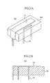
- an antenna unit 1L shown in Figs.24A and 24B can be provided, in which an antenna element 1I is mounted on a retaining member 1K previously made from an appropriate dielectric material or others, and then a feeding line 1J is arranged. The feeding line 1J is made to penetrate the retaining member 1K, and then conductibly connected to the antenna element 1I.
- This construction makes it easy to maintain a degree of parallel between the antenna element 1I and the ground pattern on a not-shown circuit substrate, avoiding the degradation of an antenna performance. Additionally, the antenna unit 1L can be handled with ease.
- FIG.25A and 25B another antenna unit 1Q shown in Figs.25A and 25B can be provided, in which an antenna element 1N is mounted on a retaining member 1M previously made from an appropriate dielectric material or others.
- a feeding line 1P is also arranged, in parallel with the antenna element 1N, spaced apart by a given distance from the antenna element 1N. Further, both ends of the feeding line 1P are made to penetrate the retaining member 1M to complete the antenna unit 1Q.
- This construction makes it easy to maintain a degree of parallel between the antenna element 1N and the ground pattern on a not-shown circuit substrate, avoiding the degradation of an antenna performance. Additionally, the antenna unit 1L can be handled with ease.
Abstract
Description
- The present invention relates to an antenna device used in high-frequency radio apparatuses and a compact-size high-frequency radio apparatus which uses the antenna device, and in particular, to a very compact-size high-frequency radio apparatus such as a watch-shaped high-frequency radio apparatus and an antenna device used in high-frequency radio apparatuses.
- Conventionally, a helical dipole antenna is generally used as an antenna for portable devices such as cellular phones which belongs to high-frequency radio apparatuses.
- The helical dipole antenna is configured in a manner that it is drawn out from or kept contained into the case of a portable device when used.
- Furthermore, as disclosed in Japanese Patent Laid-Open Publication No.3-175826, there is also known another configuration in which another type of antenna is disposed within the case of a portable device so as to form a diversity together with a helical dipole antenna. As such an antenna for high-frequency radio apparatuses, which is incorporated within the case, an inverted-F antenna has been used.
- A thin card type portable apparatus for 2.4[GHz] band employs a chip antenna using ceramic material.
- However, the above-stated helical dipole is still large to apparatuses such as watch-size portable apparatuses which are demanded to be more compact. It is difficult to simply incorporate the helical dipole antenna into the apparatus case.
- The degree of freedom for arrangement is low in the inverted-F antenna, since both its antenna element and its ground plate (main plate) are formed as an integral unit. As a result, the inverted-F antenna is difficult to be made compact any more.
- On the other hand, in the case of the ceramic chip antenna, although the chip antenna itself can be surface-mounted, an antenna including its peripheral circuit is still large as a part. In addition, the chip antenna is fairly high in cost.
- An object of the present invention is therefore to provide an antenna device for a high-frequency radio apparatus, a high-frequency radio apparatus, and a watch-shaped radio apparatus, which can be made more compact, increase sensitivity of the apparatus, and be prevented from being damaged by static electricity.
- A first aspect of the present invention is characterized in that an antenna device for a high-frequency radio apparatus connected to both an earth pattern and a feeding point formed on a circuit substrate, comprising: a metal-made antenna element whose one end is connected to the earth pattern and folded in an L-shape in section; and a feeding line whose one end is connected to the feeding point and whose other end is electrically fixedly connected to a position on the antenna element, the position being corresponding to a predetermined value of impedance of the antenna device for the high-frequency radio apparatus.
- A second aspect of the present invention is characterized in that, in the first aspect of the present invention, an orthogonal projection of the antenna element which is made onto the earth pattern serving as a surface of projection is included in the earth pattern.
- A third aspect of the present invention is characterized in that, in the first aspect of the present invention, an orthogonal projection of the antenna element which is made onto the earth pattern serving as a surface of projection is smaller in area than the earth pattern.
- A fourth aspect of the present invention is characterized in that, in the first aspect of the present invention, the antenna element is shaped into a lead wire.
- A fifth aspect of the present invention is characterized in that, in the first aspect of the present invention, a dielectric member is arranged in the vicinity of the antenna element so as to set a resonance frequency of the antenna device for the high-frequency radio apparatus to a predetermined resonance frequency.
- A sixth aspect of the present invention is characterized in that, in the fifth aspect of the present invention, a dielectric constant of the dielectric member is set in accord with the resonance frequency.
- A seventh aspect of the present invention is characterized in that, in the fifth aspect of the present invention, the dielectric member is arranged closely to the antenna element and a closely arranged state of the dielectric member is determined in accord with the resonance frequency.
- An eighth aspect of the present invention is characterized in that, in the fifth aspect of the present invention, a dielectric member for securing a display device,a substrate, a battery, or other components is arranged in the vicinity of the antenna element.
- A ninth aspect of the present invention is characterized in that, in the first aspect of the present invention, length of the antenna element is set to length of approximately a quarter of a wavelength of frequency to be used.
- A tenth aspect of the present invention is characterized in that the high-frequency radio apparatus having the antenna device according to the first aspect of the present invention, comprising: a circuit substrate on which various electrical circuits are mounted; and a display device for displaying various pieces of information, the display device being arranged in a space to one side of the circuit substrate, wherein the antenna device is arranged on the side of the display device of the circuit substrate.
- An eleventh aspect of the present invention is characterized in that, in the tenth aspect of the present invention, comprising: a case body containing the antenna device, the display device, and the circuit substrate; a case back, made of conductive material, constituting a case together with the case body; and a battery for supplying power to drive the high-frequency radio apparatus, wherein the case back is conductibly connected to either an earth potential of the circuit substrate or one electrode of the battery connected in AC (alternating current) to the earth potential.
- An twelfth aspect of the present invention is characterized in that, an antenna device for a high-frequency radio apparatus connected to both an earth pattern and a feeding point formed over an approximately overall area of at least any one layer of plural layers included in a multilayer circuit substrate, comprising: a metal-made antenna element whose one end is connected to the earth pattern and folded in an L-shape in section; and a feeding line whose one end is connected to the feeding point and whose other end is electrically fixedly connected to a position on the antenna element, the position corresponding to a predetermined value of impedance of the antenna device for the high-frequency radio apparatus.
- A thirteenth aspect of the present invention is characterized in that, in the twelfth aspect of the present invention, an orthogonal projection of the antenna element which is made onto the earth pattern serving as a surface of projection is included in the earth pattern.
- A fourteenth aspect of the present invention is characterized in that, in the twelfth aspect of the present invention, an orthogonal projection of the antenna element which is made onto the earth pattern serving as a surface of projection is smaller in area than the earth pattern.
- A fifteenth aspect of the present invention is characterized in that, in the twelfth aspect of the present invention, the antenna element is shaped into a lead wire.
- A sixteenth aspect of the present invention is characterized in that, in the twelfth aspect of the present invention, a dielectric member is arranged in the vicinity of the antenna element so as to set a resonance frequency of the antenna device for the high-frequency radio apparatus to a predetermined resonance frequency.
- A seventeenth aspect of the present invention is characterized in that, in the sixteenth aspect of the present invention, a dielectric constant of the dielectric member is set in accord with the resonance frequency.
- An eighteenth aspect of the present invention is characterized in that, in the sixteenth aspect of the present invention, the dielectric member is arranged closely to the antenna element and a closely arranged state of the dielectric member is determined in accord with the resonance frequency.
- A nineteenth aspect of the present invention is characterized in that, in the twelfth aspect of the present invention, the dielectric member is configured so as to secure a display device, substrate, a battery, and other components.
- A twentieth aspect of the present invention is characterized in that, in the twelfth aspect of the present invention, length of the antenna element is set to length of approximately a quarter of a wavelength of frequency to be used.
- A twenty-first aspect of the present invention is characterized in that the high-frequency radio apparatus having the antenna device according to the twenty aspect of the present invention, comprising: a circuit substrate on which various electrical circuits are mounted; and a display device for displaying various pieces of information, the display device being arranged in a space to one side of the circuit substrate, wherein the antenna device is arranged on the side of the display device of the circuit substrate.
- A twenty-second aspect of the present invention is characterized in that, in the twenty-first aspect of the present invention, comprising: a case body containing the antenna device, the display device, and the circuit substrate; a case back, made of conductive material, constituting a case together with the case body; and a battery for supplying power to drive the high-frequency radio apparatus, wherein the case back is conductibly connected to either an earth potential of the circuit substrate or one electrode of the battery connected in AC (alternating current) to the earth potential.
- A twenty-third aspect of the present invention is characterized in that, an antenna device for a high-frequency radio apparatus connected to both an earth pattern and a feeding point formed on a circuit substrate, comprising: a metal-made antenna element whose one end is connected to the earth pattern and folded in an L-shape in section; and a feeding line whose one end is connected to the feeding point and whose other end is fixedly connected to the earth pattern.
- A twenty-fourth aspect of the present invention is characterized in that, in the twenty-third aspect of the present invention, the earth pattern is composed of an electrode pattern formed on the circuit substrate.
- A twenty-fifth aspect of the present invention is characterized in that, in the twenty-fourth aspect of the present invention, the earth pattern is formed over an approximately overall range of a surface positioned under the antenna element.
- A twenty-sixth aspect of the present invention is characterized in that, in the twenty-third aspect of the present invention, length of the antenna element is set to length of approximately a quarter of a wavelength of frequency to be used.
- A twenty-seventh aspect of the present invention is characterized in that, comprising: a wristwatch-shaped case; an antenna device for a high-frequency radio apparatus defined by the twenty-third aspect of the present invention, wherein the antenna device for the high-frequency radio apparatus is arranged within the wristwatch-shaped case.
- A twenty-eighth aspect of the present invention is characterized in that, comprising: a case; a substrate having an earth pattern and being arranged within the case; an antenna element whose one end is electrically connected to the earth pattern, the antenna element being arranged three-dimensionally to the circuit substrate, and partially arranged on an upper surface of the case; and a feeding line whose one end is connected to the earth pattern, whose other end is connected to a feeding point, and the feeding line being arranged three-dimensionally to the circuit substrate in parallel to a direction connecting one end side and the other end side of the antenna element.
- A twenty-ninth aspect of the present invention is characterized in that, in the twenty-eight aspect of the present invention, the antenna element is made of metal material and connected to the earth pattern via a conductive member, the conductive member is made of the same metal material as that of the antenna element, and both the antenna element and the conductive member are integrally formed in an L-shape.
- A thirtieth aspect of the present invention is characterized in that,
an antenna device for a high-frequency radio apparatus according to the twenty-eighth aspect of the present invention; a circuit substrate on which a radio circuit is formed, the radio circuit being connected to the antenna device for the high-frequency radio apparatus; and a wristwatch-shaped case containing both the antenna device for the high-frequency radio apparatus and the circuit substrate. - Fig.1 shows a schematic sectional view of a watch-shaped radio apparatus according to a first embodiment.
- Fig.2 shows a schematic perspective view of the top of the watch-shaped radio apparatus according to the first embodiment.
- Fig.3A is a plan view showing an inverted-F antenna of the first embodiment.
- Fig.3B is a front view showing the inverted-F antenna of the first embodiment.
- Fig.4A is a plan view showing an inverted-F antenna of a second embodiment.
- Fig.4B is a front view showing the inverted-F antenna of the second embodiment.
- Fig.5 illustrates a mounted state of the inverted-F antenna.
- Fig.6 is a cross sectional view showing the part of an antenna of the watch-shaped radio apparatus in order to exemplify a retaining mechanism.
- Fig.7 is an illustration of another example of the retaining mechanism.
- Fig.8 is an illustration of an example for forming a ground pattern on a multilayer substrate.
- Fig.9 shows a cross section of the multilayer substrate in Fig.8.
- Fig.10 illustrates an example of a characteristic of the inverted-F antenna.
- Fig.11 shows a schematic sectional view of a watch-shaped radio apparatus according to a third embodiment.
- Fig.12 shows a schematic perspective view from the top of the watch-shaped radio apparatus.
- Fig.13A is a plan view showing an inverted-L antenna of the third embodiment.
- Fig.13B is a front view showing the inverted-L antenna of the third embodiment.
- Fig.14A is a plan view showing a mounted inverted-L antenna of a fourth embodiment.
- Fig.14B is a front view showing the mounted inverted-L antenna of the fourth embodiment.
- Fig.15 illustrates a mounted state of the inverted-L antenna.
- Fig.16A is a plan view showing an inverted-L antenna according to a fifth embodiment.
- Fig.16B is a front view showing the inverted-L antenna according to the fifth embodiment.
- Fig.17A is a plan view showing the mounted inverted-L antenna of the fifth embodiment.
- Fig.17B is a front view showing the mounted inverted-L antenna of the fifth embodiment.
- Fig.18 illustrates an example of a characteristic of the inverted-L antenna.
- Fig.19 illustrates a mounted state of the inverted-L antenna according to the fifth embodiment.
- Fig.20 is a sectional view showing a watch-shaped radio apparatus of a sixth embodiment.
- Fig.21 is a schematic perspective view from the top of the watch-shaped radio apparatus according to the sixth embodiment.
- Fig.22A is an outer oblique view (part 1) of a case on which an antenna element is secured.
- Fig.22B is an outer oblique view (part 2) of a case on which an antenna element is secured.
- Fig.23 illustrates a first modification of the embodiments.
- Fig.24A is an outer oblique view (part 1) of an antenna unit according to a second modification.
- Fig.24B is a sectional view (part 1) of the antenna unit according to the second modification.
- Fig.25A is an outer oblique view (part 2) of the antenna unit according to the second modification.
- Fig.25B is a sectional view (part 2) of the antenna unit according to the second modification.
- With reference to the accompanying drawings, preferred embodiments of the present invention will now be described.
- Fig. 1 is a schematic sectional view of a watch-shaped radio apparatus according to a first embodiment of the present invention.
- In Fig. 1, there is provided an inverted-
F antenna 1, which is formed three-dimensionally and incorporated in a watch-shapedradio apparatus 100 as an antenna device for a high-frequency radio apparatus. - The inverted-
F antenna 1 comprises anantenna element 1A and afeeding line 1B. - The
antenna element 1A is made of metal and formed into an L-shape in section. Theantenna element 1A is fixedly connected to a ground pattern (earth pattern) mounted on acircuit substrate 2. Soldering is a normal way to connect theantenna element 1A to thecircuit substrate 2. - The
feeding line 1B is conductibly secured at a given position on theantenna element 1A. - The
circuit substrate 2 of the watch-shapedradio apparatus 100 is sandwiched from its upper and lower sides byplastic members - In the
plastic member 3, amicro nut 13 is inserted and formed in advance. Thecircuit substrate 2 is secured by applying amicro screw 14 to themicro nut 13 through theplastic member 5 from under theplastic member 3. - Securing the
plastic member 3 to thecircuit substrate 2 allows aconductive rubber 12 to be pressed onto thecircuit substrate 2. By means of thisconductive rubber 12, an LCD (Liquid Crystal Display)panel 10 is electrically connected to an LCD-driving pattern mounted on thecircuit substrate 2. - An
electric circuit 8 is mounted on the lower surface of thecircuit substrate 2 and includes a radio circuit consisting of electric parts. - In Fig. 1, the
electric circuit 8 is illustrated as a rectangular module for the sake of simplifying the drawing. Instead of such a module, the parts of theelectric circuit 8 can be mounted directly on thesubstrate 2. - A
button type battery 6 is used as a power source of the watch-shaped radio apparatus. Thebutton type battery 6, which is secured on themember 5, is electrically connected to a case back 7 via a conductive plate which is not shown. - A
cover glass 9 is fixedly arranged on awatchcase 4. The display of theLCD 10 can therefore be seen through thecover glass 9. Thewatchcase 4 and the case back 7 are secured by, usually, screwing. - Fig. 2 shows a schematic perspective view of the top of the watch-shaped
radio apparatus 100. - As shown in Fig. 2, a
ground pattern 15 is formed on thecircuit substrate 2. - Since it is often the case that the watchcase itself has a curved-line shape by virtue of design, the
circuit substrate 2 is not necessarily a rectangular. However in many cases, it may be formed into a curved outer shape or folded-line outer shape. Accordingly, arranging parts and an electrode pattern such as theground pattern 15 on thecircuit substrate 2 in agreement with the shape of thecircuit substrate 2 leads to effective utilization of the substrate area for miniaturizing the apparatus. - Fig. 3A is a plan view of the inverted-
F antenna 1 of the first embodiment, while Fig.3B is a front view thereof. - The inverted-
F antenna 1 comprises, as descried above, theplate antenna element 1A folded into an L-shape at one end and thefeeding line 1B. - It is preferable that the
antenna element 1A be made of materials, such as copper, whose conductivity is high. It is also possible to use high-conductivity materials as the surface plating. - The
feeding line 1B is conductibly secured at a position on the inverted-F antenna 1A in a way that the inverted-F antenna 1A may have a predetermined value of impedance after its securing. The value of impedance is, for example, 50 [Ω]. Thefeeding line 1B is perpendicularly linked to theantenna element 1A. - In order to keep electric resistance to be low, it is preferred that
antenna element 1A and feedingline 1B be connected to each other by brazing or soldering. - Figs. 4A and 4B show a second embodiment of the present invention. In these Figs. 4A and 4B, the same or identical reference numerals as to those in Figs. 1 to 3 are shown with the same reference numerals.
- Fig. 4A is a plan view showing a mounted state of the inverted-
F antenna 1 according to the second embodiment. Fig. 4B is, on the other hand, is a front view showing the mounted state of the inverted-F antenna 1 of the second embodiment. - On the upper surface of a
circuit substrate 21, an electric conductor pattern (plane electrodes) 22 is arranged. - One end of the
antenna element 1A is conductibly secured to theconductor pattern 22. - The
feeding line 1B is conductibly connected to afeeding terminal pattern 23 mounted on thecircuit substrate 21. In this configuration, it is also possible to use a hole pattern as the feedingterminal pattern 23, which is a through hole formed through thecircuit substrate 21, and solder thefeeding line 23, after inserted into the hole pattern. - Further, the feeding
terminal pattern 23 is linked to the ground (earth) potential in DC (direct current) to a signal supplied from the inverted-F antenna 1. - For the sake of easier understanding, Figs. 4A and 4B does not show circuit parts and other structural components structured on the
circuit substrate 21, but only show the antenna part. - The length of the
antenna element 1A, which composes the inverted-F antenna 1, is approximately a quarter of a wavelength of a frequency to be used, including its folded portion; for example, approximately 3 [cm] at a frequency of 2.5 [GHz]. - The
feeding line 1B is connected to a position on theantenna element 1A so that the position corresponds to a predetermined value of impedance (for example, 50 [Ω]) to the ground potential in the vicinity of the feedingterminal pattern 23. - Impedance values of circuit terminals and wiring are determined so that the impedance of signal lines connecting with the feeding
terminal pattern 23 from a not-shown circuit is also set to an identical value (for example, 50 [Ω]). - Specifically, concerning signal lines connected to the feeding
terminal pattern 23, it is preferable, in matching the inverted-F antenna 1 with the signal lines, that the signal lines be formed by strip lines, with a given value of impedance, arranged on the back (not shown) of thecircuit substrate 21 - Theoretically, it is best that the inverted-
F antenna 1 be arranged at the center of the ground pattern of thecircuit substrate 21. However, it is usually difficult to arrange the antenna at the center of thecircuit substrate 21, due to the arrangement of the other parts, for miniaturizing the total size of the apparatus. - Therefore, it is enough to provide a configuration that the orthogonal projection of the
antenna element 1A, whose projected plane is on the ground pattern, is included in the ground pattern. - Alternatively, it is enough to provide a configuration that the orthogonal projection of the
antenna element 1A, whose projected plane is on the ground pattern, is smaller in area than the ground pattern. - Practical examples of such configurations will now be described, in which the orthogonal projection of the
antenna element 1A, whose projected plane is on the ground pattern, is included in the ground pattern, or, the orthogonal projection of theantenna element 1A, whose projected plane is on the ground pattern, is smaller in area than the ground pattern. - Fig. 5 illustrates a mounted state of the inverted-F antenna.
- On the upper surface of the
circuit substrate 2, aground pattern 15 is mounted at a position facing theantenna element 1A. - In addition, on the upper surface of the
circuit substrate 2, drivesignal electrode patterns 16 are mounted for drive signals to drive theLCD 10. - Wiring to the
LCD 10 of a compact apparatus having an LCD panel is usually realized by connecting drive signal electrodes embedded in theLCD 10 itself and the drivesignal electrode patterns 16 mounted on the upper surface of thecircuit substrate 21 via the conductive rubber 21 (refer to Fig. 1). - In general, the
LCD 10 that functions as a user interface of the apparatus is arranged at the center thereof. In the case of such an arrangement, the drivesignal electrode patterns 16 and a display driver for generating drive signals or a CPU including a display driver, which are not shown, are arranged on the back of theLCD 10. Thus, the area on thecircuit substrate 2, which corresponds to theLCD 10, is occupied by wiring for connecting the drivesignal electrode patterns 16 and the CPU. - In this case, a multilayer substrate may be used to arrange such a wiring section on another layer utilizing through holes.
- However, this method still requires the same substrate area compared to a wiring configuration without a multilayer substrate. This means that utilizing a multilayer substrate does not contribute to the reduction of the area used on the substrate.
- After all, this results in that the central part on the upper surface of the
circuit substrate 2 is occupied by the drivesignal electrode patterns 16 of theLCD 10. Thus, there arises a restriction that the inverted-F antenna 1 and theground pattern 15 have to be arranged at either one end of thecircuit substrate 2. - The
ground pattern 15 shown in Fig.5 is mounted in some shape, not necessarily rectangular, at one end of the upper surface of thecircuit substrate 2. - In this case, the orthogonal projection of the
antenna element 1A, whose projected plane is on the ground pattern, is included in theground pattern 15. Alternatively, the orthogonal projection of theantenna element 1A, whose projected plane is on the ground pattern, is smaller in area than theground pattern 15. - A practical example is that, when a frequency to be used is 2.5 [GHz], a length of the
antenna element 1A is approximately 28 [mm] in its longitudinal direction and a height from thecircuit substrate 2 is 2 [mm]. Under such conditions, the antenna device can be configured to have theantenna element 1A whose width is approximately 2 [mm]. - When taking it account that the member composing the
antenna element 1A has enough strength, a thickness of theantenna element 1A can be set to approximately 0.2 [mm]. - Incidentally, it is possible that the width and thickness of the antenna element are determined to optimum values based on conditions, such as physical strength of material composing the
antenna element 1A, spacing allowed on thecircuit substrate 2, and a necessary antenna gain. When theantenna element 1A is made up of urethane-coated copper wire, there are advantages in size, workability, and manufacturing cost. - A retaining mechanism of the antenna used in the first and second embodiments will now be described.
- Fig. 6 is a sectional view showing only the peripheral part of the
antenna element 1A shown in Fig. 1. - The
antenna element 1A positioned over thecircuit substrate 2 is retained from the upper side thereof by the plastic member 3 (hatched part) which also functions as a securing frame for theLCD 10. This retainment prevents theantenna element 1A from moving upward from thecircuit substrate 2. - An approximately parallel part of the
antenna element 1A to thecircuit substrate 2 is therefore kept parallel to thecircuit substrate 2. The inverted-F antenna 1 thus constructed has minimal variation in a degree of parallel to thecircuit substrate 2 when the antenna is mounted. As a result, variation in the characteristics of the inverted-F antenna 1 can be reduced. - Fig. 7 illustrates another example of the retaining mechanism.
- In this example, as shown in Fig. 7, the plastic member shown in Fig. 6 is replaced by a
plastic member 3B which also loads plastic material beneath the antenna element. If taking the structure into consideration, part of the watchcase may be used as a plastic member having the above function. - Thus, the
plastic member 3B retains theantenna element 1A from its upper and lower sides. - This structure prevents the
antenna element 1A from being deformed from its upper and lower sides. - Accordingly, the deformation of the antenna can be suppressed further.
- It is well known that the wavelength of a high-frequency signal is shortened by the impedance of the space through which the signal is transmitted.
- When placing a dielectric member around the antenna, the wavelength of a frequency to be used is therefore shortened according to a dielectric constant of the dielectric member around the antenna.
- Accordingly, when a section of the
plastic member antenna element 1A, is set to have an optimum area, the length of the element that resonates at a desired frequency in the air can adequately be adjusted to a shorter value. - In addition, changing materiel of the
plastic member - The above retaining mechanism is able to provide compact antennas, without particular manufacturing process such as a ceramic chip antenna. In particular, by using a feature of a dielectric such as plastic which is usually used in the watch-shaped
radio apparatus 100, the antenna can be made compact so as to have a practical size, without increasing manufacturing cost unnecessarily. - A plastic member is generally used as a securing member incorporated within apparatuses including digital watches and compact information devices. In this respect, however, the securing member is not limited to one made of plastic. Various kinds of members made of different dielectric members are usable for shortening the antenna. It is therefore preferable that the securing member be chosen with consideration of excellence in workability, incombustibility, cost, and others.
- How to form the ground pattern will now be described.
- Fig. 8 is an illustration showing an example of forming the ground pattern for a multilayer substrate. Fig. 9 is a sectional view of the multilayer substrate shown in Fig. 8.
- In Fig. 8, a
circuit substrate 2A is a multilayer substrate, in which, as shown in Fig. 9, circuit patterns can be mounted on inner layers as well as its surface. - More specifically, a
ground pattern 17 is mounted over the almost entire surface of at least one of the inner layer substrates. - The
ground pattern 17 is connected to theground pattern 15 formed on the front surface of thecircuit substrate 2A via a plurality of throughholes 18. - The area of the
ground pattern 15 is restricted by the drivesignal electrode patterns 16 of theLCD 10, as described before. As shown in Fig.8, theground pattern 15 is therefore made larger in area than, at least, the orthogonal projection of theantenna element 1A to theground pattern 15. In addition, a conductive connection with theground pattern 17 on inner layers provides a larger ground pattern area. To obtain a sufficient ground pattern area to theantenna element 1A, it is therefore preferable that the area of theground pattern 17 on inner layers spread over the almost entire surface on the inner layers. Alternatively, if there is a margin for an antenna gain owing to the system configuration of the watch-shapedradio apparatus 100, the inner substrates are partly used for other wiring patterns. - Fig. 10 exemplifies a radiation pattern of the thus-constructed inverted-F antenna device.
- The characteristic is changed correspondingly to the shape of a case when the watch-shaped
radio apparatus 100 is practically produced. With this respect considered, Fig. 10 exemplifies a radiation pattern of only an inner circuit module excluding the case back 7 (refer to Fig.1). This result reveals that a direction showing a maximum gain is different from that of a dipole antenna, because there is an influence from parts other than the antenna. - However, it is understood that the radiation pattern has no problem for practical uses.
- Wearing a wristwatch-shaped radio apparatus according to the embodiments of the present invention on the user's wrist will now be described.
- In Fig. 1, the case back 7 made of metal such as stainless steel is positioned beneath the watch-shaped radio apparatus according to the embodiments of the present invention.
- The case back 7 is conductibly connected to the positive electrode of the
battery 6 by way of terminal plates or others. The negative electrode of thebattery 6 is electrically connected to the ground pattern of thecircuit substrate 2 by way of terminal plates or others. Similarly, the positive electrode of thebutton type battery 6 is also electrically connected to a power source on thecircuit substrate 2 through terminal plates or others. A by-pass capacitor is normally electrically connected between a power source terminal and a ground terminal, thereby the circuit being stabilized by a reduced value of impedance of the power source. In the case of such high-frequency apparatuses, the patterns of the ground and power source are considered to have the same potential in AC (alternating current) to the earth potential. - By the way, in cases where the watch-shaped
radio apparatus 100 configured as shown in Fig.8 is worn on the user's wrist, the inverted-F antenna 1 is located on the upper side of the apparatus, which is spaced apart from the wrist. In contrast, theground pattern 15 mounted on the upper surface of thecircuit substrate 2A is positioned under the inverted-F antenna 1. - Further, a ground pattern is positioned on inner layers of the
circuit substrate 2A. Further, under the ground pattern formed on the inner layers, thebattery 6 and also the case back 7, having a larger area, are positioned. As stated above, the metal-made case back 7 can be regarded as being the same in potential in AC as the ground pattern of thecircuit substrate 2A. That is, the metal-made case back 7 has the effect to widen the ground area to the inverted-F antenna 1. - Moreover, this wearing results in that the user's body (arm) is connected to the ground potential of the antenna via the case back 7. The user's body itself can be considered the ground when the apparatus is worn by a user, thus providing a configuration in which the ground area is further widened to the antenna.
- The foregoing first and second embodiments are able to provide the advantages as bellow.
- (1) There can be provided a compact-size radio apparatus having an inverted-F antenna integrally formed with a circuit substrate.
- (2) The size of the antenna element can be shortened than that required in the air by placing a dielectric member around the antenna, so that a compact radio apparatus can be provided.
- (3) Additionally, as the dielectric member placed around the antenna, a securing member disposed in the apparatus can be used in common. Therefore, it is possible to provide radio apparatuses which are made compact by an efficient use of the inner space and which exhibit stabilized antenna characteristics of which variations being adjusted by the use of an antenna retaining mechanism.
- (4) The antenna is arranged over the upper surface of the substrate, while the ground pattern, battery, and metal-made case back are arranged in turn from beneath the substrate. This results in that, when the apparatus is worn by a user, a portion positioned under the substrate, including the user's body, is given the ground potential. Therefore, a compact radio apparatus can be provided, which has a larger ground area to the antenna element when worn on the user's body.
- (5) Making an antenna compact is prerequisite for miniaturization of a radio apparatus. It is considered that an operating frequency is raised to attain such a compact apparatus. However, the operating frequency has already been assigned to a given value by regulations and others, so no choice can be done freely.
-
- Therefore, in order to make a smaller antenna under the predetermined regulations and to raise an antenna gain at the same time, the following points have to be taken into consideration.
- The consideration should be given to the configuration of the antenna itself, how to form the ground, and a relationship with members positioned around the antenna.
- Furthermore, in the case that the apparatus is designed to be worn by a user, a relationship with the human body must be taken into consideration so as to accomplish an optimum antenna operation.
- As described above, the antenna is optimized with respect to a relationship with its constituents, and there can be provided a compact radio apparatus whose operating characteristics are stable even when a user wears the apparatus.
- The inverted-
F antenna 1 in the first and second embodiments has been constructed three-dimensionally, in which the feeding line should be connected to the antenna perpendicularly. - This structure causes the distance between the antenna element and the substrate to be longer and the feeding line to be longer. It becomes therefore difficult to realize a given value of the strength of the antenna itself and to hold the antenna in parallel to the ground.
- Additionally, when arranging the antenna outside the case, there is a possibility that the structure becomes complicated, because a connecting portion between the feeding line and the antenna should be placed outside the case as well.
- This will raise a possibility that the static electricity reaches the radio circuit through the feeding line and the radio circuit is damaged, when the static electricity is attracted to the antenna in a case where the feeding line connects the antenna with the radio circuit.
- Accordingly, in place of the
feeding line 1B described in the first or second embodiment, a third embodiment adopts afeeding line 1C arranged in parallel with theantenna element 1A (refer to Fig. 11). - Fig. 11 is a schematic sectional view of a watch-shaped radio apparatus according to the third embodiment of the present invention. Fig. 11 has the same or identical reference numerals as to those in the first embodiment shown in Fig. 1, which are represented by the same reference numerals.
- As shown in Fig. 11, an inverted-
L antenna 51 is configured three-dimensionally as an antenna device for a high-frequency radio apparatus, which is incorporated in a watch-shapedradio apparatus 100A. - Fig. 12 shows a schematic perspective view of the top of the watch-shaped
radio apparatus 100A. - As shown in Fig. 12, a
ground pattern 15 is mounted on thecircuit substrate 2. - Fig. 13A is a plan view of the inverted-
L antenna 51 of the third embodiment, while the Fig. 13B is a front view thereof. - The inverted-
L antenna 51 comprises, as stated above, a plate-like antenna element 1A whose one end is folded in the L-shape, and afeeding line 1C arranged so as to be in parallel with a longitudinal section of theantenna element 1A at a position spaced apart by a predetermined distance from theantenna element 1A. - The
feeding line 1C is secured at a position that provides a given value of impedance of the inverted-L antenna 51 after being secured. The impedance value is 50 [Ω], for example. - Figs. 14A and 14B show a fourth embodiment of the present invention. In Figs. 14A and 14B, the same or identical reference numerals as to those in Figs. 11, 12, 13A or 13B are shown with the same reference numerals.
- Fig. 14A is a plan view showing the mounted-state inverted-
L antenna 51 according to the fourth embodiment. Fig. 14B is a front view showing the mounted-state inverted-L antenna 51 of the fourth embodiment. - On the upper surface of the
circuit substrate 21, the electric conductor pattern (plane electrodes) 22 is mounted. - One end of the
antenna element 1A is conductibly secured to theconductor pattern 22. - The
feeding line 1C is conductibly connected to afeeding terminal pattern 23 mounted on thecircuit substrate 21. In accomplishing this configuration, it is also possible to use a hole pattern as the feedingterminal pattern 23, which is a through hole formed through thecircuit substrate 21, and solder thefeeding line 1B after inserted into the hole pattern. - Further, the feeding
terminal pattern 23 is linked to the ground (earth) potential in DC (direct current) to a signal supplied from the inverted-L antenna 51. - For the sake of easier understanding, Figs. 14A and 14B do not show circuit parts and other structural components on the
circuit substrate 21, but show only the antenna part. - The length of the
antenna element 1A which composes the inverted-L antenna 51 is approximately a quarter of a wavelength of a frequency to be used, including its folded portion; for example, approximately 3 [cm] at a frequency of 2.5 [GHz]. - The
feeding line 1C is connected to a position on theantenna element 1A so that the position corresponds to a predetermined value of impedance (for example, 50 [Ω]) to the ground potential in the vicinity of the feedingterminal pattern 23. - Impedance values of circuit terminals and wiring are determined so that the impedance of signal lines connecting with the feeding
terminal pattern 23 from a not-shown circuit is also set to an identical value (for example, 50 [Ω]). - Specifically, concerning signal lines connected to the feeding
terminal pattern 23, it is preferable, in matching the inverted-L antenna 51 with the signal lines, that the signal lines be formed by strip lines, with a given value of impedance, arranged on the back (not shown) of thecircuit substrate 21. - Theoretically, it is best that the inverted-
L antenna 51 be arranged at the center of the ground pattern of thecircuit substrate 21. However, it is usually difficult to arrange the antenna at the center of thecircuit substrate 21, due to the arrangement of the other parts, for miniaturizing the total size of the apparatus. - Therefore, it is enough to provide a configuration that the orthogonal projection of the
antenna element 1A, whose projected plane is on the ground pattern, is included in the ground pattern. - Alternatively, it is enough to provide a configuration that the orthogonal projection of the
antenna element 1A, whose projected plane is on the ground pattern, is smaller in area than the ground pattern. - Practical examples of configurations will now be described, in which the orthogonal projection of the
antenna element 1A, whose projected plane is on the ground pattern, is included in the ground pattern, or, the orthogonal projection of theantenna element 1A, whose projected plane is on the ground pattern, is smaller in area than the ground pattern. - Fig. 15 illustrates a mounted state of the inverted-L antenna.
- On the upper surface of the
circuit substrate 2, aground pattern 15 is mounted at a position facing theantenna element 1A. - In addition, on the upper surface of the
circuit substrate 2, drivesignal electrode patterns 16 is mounted for drive signals to drive theLCD 10. - Wiring to the
LCD 10 of a compact apparatus having an LCD panel is usually realized by connecting drive signal electrodes embedded in theLCD 10 itself and the drivesignal electrode patterns 16 mounted on the upper surface of thecircuit substrate 2 via the conductive rubber 21 (refer to Fig.1). - In general, the
LCD 10 that functions as a user interface of the apparatus is arranged at the center thereof. In the case of such an arrangement, the drivesignal electrode patterns 16 and a display driver for generating drive signals or a CPU including a display driver, which is not shown, are arranged on the back of theLCD 10. Thus, the area on thecircuit substrate 2, which corresponds to theLCD 10, is occupied by wiring for connecting the drivesignal electrode patterns 16 and the CPU. - The
ground pattern 15 as shown in Fig.15 is mounted in a shape, not necessarily rectangular, at one end of the upper surface of thecircuit substrate 2. - In this case, the orthogonal projection of the
antenna element 1A, whose projected plane is on the ground pattern, is included in theground pattern 15. Alternatively, the orthogonal projection of theantenna element 1A, whose projected plane is on the ground pattern, is smaller in area than theground pattern 15. - Figs. 16A and 16B show a fifth embodiment of the present invention. In Figs. 16A and 16B, the same or identical reference numerals as to those in Figs. 11, 12, 13A or 13B are shown with the same reference numerals.
- In the configuration shown in Fig.16A, an inverted-
L antenna 71 comprises anantenna element 1D composed of an L-shaped wire and afeeding line 1C composed of an approximately U-shaped wire. - The
antenna element 1D and thefeeding line 1C can easily be formed by, for example, bending wires such as urethane-coated copper wires. - As shown in Figs. 16A and 16B, the
feeding line 1C is arranged so that its longitudinal direction becomes parallel with theantenna element 1D, along by a side of theantenna element 1D. - In addition, the
feeding line 1C is arranged so that it keeps a proper electric coupling with theantenna element 1D. Practically, as shown in Figs. 17A and 17B, one end of thefeeding line 1C is electrically connected with thefeeding point 23, while the other end is electrically connected with theground pattern 22. This arrangement permits the impedance observed from thefeeding point 23 to be set to a desired value (for example, 50 [Ω]) at a frequency to be used. - An example of a radiation pattern of the inverted-
L antenna 71 thus-constructed is shown in Fig.18. - As shown in Fig.18, although the gain in a directional range of 135 to 225 degrees may be worse than that of a dipole antenna, the gain in the remaining directional range is better than that of a dipole antenna.
- Fig. 19 shows an example of arranging the antenna on the substrate, when the antenna device described in the fifth embodiment is incorporated into a wristwatch-shaped radio apparatus.
- The
feeding line 1C is arranged in parallel with a side of theantenna element 1D of the inverted-L antenna 71, and one end of thefeeding line 1C is electrically connected with thefeeding point 23, whilst the other end is electrically connected to theground pattern 15 which is mounted under theantenna element 1D. - In the case of Fig. 19, only a set of the
antenna element 1D, feedingline 1C, andLCD drive electrodes 16 are depicted. It is preferable that theantenna element 1D be retained in parallel to theground pattern 15 with the help of a plastic member or others. - Fig. 20 is a schematic sectional view showing a watch-shaped radio apparatus of a sixth embodiment, and Fig. 21 is a schematic perspective view from the top thereof.
- The sixth embodiment concerns an arrangement of an inverted-L antenna, in which part of an
antenna element 1E thereof, which is parallel with theground pattern 15 on thecircuit substrate 2, is placed on the upper surface of the case. - Practically, one end of an L-shaped antenna element penetrates the
case 4 to be connected to the ground pattern in the case. Afeeding line 1F is placed under theantenna element 1E spaced apart therefrom. Thefeeding line 1F, which is parallel with theantenna element 1E, is placed non-contacted with theantenna element 1E. Thus, signals induced in theantenna element 1E are transmitted to each circuit on thecircuit substrate 2 via thefeeding line 1F. As shown in Fig. 22A, anantenna element 1E can be arranged to partly come out from thecase 4 or can be made of a conductor electrode formed on the upper surface of thecase 4 by means of, for example, vapor deposition. In the latter case, theantenna element 1E, which is the conductor electrode on the upper surface of the case, is connected to the ground pattern in the case through a conductor 1EC, as illustrated in Fig.22B. If a metal plate is arranged on the upper surface of thecase 4, a screw to fasten the metal plate may be made to penetrate thecase 4 and connect with the ground pattern in thecase 4. - In cases where the antenna device according to the present invention is embedded in a watch-shaped radio apparatus, an attention how to arrange the antenna has to be paid, because members surrounding the antenna may have a greater influence on its characteristics.
- Members which exert influence upon the characteristics of the antenna include the plastic member closed to the antenna, case, battery, and case back. To avoid these influence, it may be considered that the antenna be arranged as far from the substrate as possible. The antenna thus arranged is easier to optimize, because influences on the antenna, which arises from members surrounding the antenna, are lessened. Additionally, since there is also no member which covers the antenna, better sensitivity of the antenna can be easily obtained.
- Alternatively, in cases where the antenna is placed outside the case, it should be considered that static electricity may be induced in the antenna. In general, static electricity induced by the human body is estimated to have about 10 [kV], in some cases, reaching 30 [kV].
- Therefore, it is not preferable to place the antenna element and the feeding line, conductibly connecting to the circuit feeding point, outside the case as in the inverted-F antenna, because static electricity is easily attracted to the circuit.
- In contrast, the antenna and feeding line structure of the third to sixth embodiments are constructed in consideration of these conditions. The antenna element is electrically connected to the ground pattern on the circuit substrate in a direct manner and electric charges flow outside the case through the ground pattern, while signals induced by the antenna element are sent to the circuit by way of the non-contact feeding line.
- Accordingly, the third to sixth embodiments have the advantages described below.
- (1) Compared to the inverted-F antenna, the inverted-L antenna is simple, thus making it easier to produce the antenna and lowering cost.
- (2) Arranging the antenna outside the case makes it difficult to have influence from members surrounding the antenna and leads to an easy optimization.
- (3) Arranging the antenna outside the case makes it difficult to have influence from members surrounding the antenna and leads to a higher possibility of improving the sensitivity of the antenna.
- (4) Though the antenna is placed outside the case, the antenna element is connected to the ground and signals are transmitted by using the feeding line mounted with no contact to the antenna element. This prevents the circuit from being damaged due to the static electricity.
- (5) Because the antenna element is placed outside the case, the inner space of the case can be saved, thus raising the degree of freedom for arranging the other parts, thus making the apparatus more compact.
- (6) Where an antenna according to the present invention is practiced into a watch, the antenna is arranged outside the case. Therefore, influences on the antenna, which are caused from the user's body when a user wears the watch, can be lessened, increasing the sensitivity of the antenna.
-
- In the foregoing first and second embodiments, the plate-like electrode is used as the antenna element. However, it is possible that, for example, as shown in Fig.23, an
antenna element 1G is made from a wire and conductibly connected to afeeding line 1H made from a wire as well. - In the foregoing embodiments, one end of the antenna element is formed into a free end. Instead, an
antenna unit 1L shown in Figs.24A and 24B can be provided, in which an antenna element 1I is mounted on a retainingmember 1K previously made from an appropriate dielectric material or others, and then afeeding line 1J is arranged. Thefeeding line 1J is made to penetrate the retainingmember 1K, and then conductibly connected to the antenna element 1I. - This construction makes it easy to maintain a degree of parallel between the antenna element 1I and the ground pattern on a not-shown circuit substrate, avoiding the degradation of an antenna performance. Additionally, the
antenna unit 1L can be handled with ease. - Furthermore, appropriately selecting a material of the retaining
member 1K from a viewpoint of factors such as a dielectric constant leads to a more compact apparatus, with keeping the same resonant frequency to be used is the same. - Alternatively, another
antenna unit 1Q shown in Figs.25A and 25B can be provided, in which anantenna element 1N is mounted on a retainingmember 1M previously made from an appropriate dielectric material or others. In this antenna unit, afeeding line 1P is also arranged, in parallel with theantenna element 1N, spaced apart by a given distance from theantenna element 1N. Further, both ends of thefeeding line 1P are made to penetrate the retainingmember 1M to complete theantenna unit 1Q. - This construction makes it easy to maintain a degree of parallel between the
antenna element 1N and the ground pattern on a not-shown circuit substrate, avoiding the degradation of an antenna performance. Additionally, theantenna unit 1L can be handled with ease.
Claims (30)
- An antenna device for a high-frequency radio apparatus connected to both an earth pattern and a feeding point formed on a circuit substrate, comprising:a metal-made antenna element whose one end is connected to the earth pattern and folded in an L-shape in section; anda feeding line whose one end is connected to the feeding point and whose other end is electrically fixedly connected to a position on the antenna element, the position being corresponding to a predetermined value of impedance of the antenna device for the high-frequency radio apparatus.
- An antenna device for a high-frequency radio apparatus of claim 1, wherein an orthogonal projection of the antenna element which is made onto the earth pattern serving as a surface of projection is included in the earth pattern.
- An antenna device for a high-frequency radio apparatus of claim 1, wherein an orthogonal projection of the antenna element which is made onto the earth pattern serving as a surface of projection is smaller in area than the earth pattern.
- An antenna device for a high-frequency radio apparatus of claim 1, wherein the antenna element is shaped into a lead wire.
- An antenna device for a high-frequency radio apparatus of claim 1, wherein a dielectric member is arranged in the vicinity of the antenna element so as to set a resonance frequency of the antenna device for the high-frequency radio apparatus to a predetermined resonance frequency.
- An antenna device for a high-frequency radio apparatus of claim 5, wherein a dielectric constant of the dielectric member is set in accord with the resonance frequency.
- An antenna device for a high-frequency radio apparatus of claim 5, wherein the dielectric member is arranged closely to the antenna element and a closely arranged state of the dielectric member is determined in accord with the resonance frequency.
- An antenna device for a high-frequency radio apparatus of claim 5, wherein a dielectric member for securing a display device, substrate, a battery, or other components is arranged in the vicinity of the antenna element.
- An antenna device for a high-frequency radio apparatus of claim 1, wherein length of the antenna element is set to length of approximately a quarter of wavelength of frequency to be used.
- A high-frequency radio apparatus having an antenna device of claim 1, comprising:a circuit substrate on which various electrical circuits are mounted; anda display device for displaying various pieces of information, the display device being arranged in a space to one side of the circuit substrate,wherein the antenna device is arranged on the side of the display device of the circuit substrate.
- A high-frequency radio apparatus of claim 10, comprising:a case body containing the antenna device, the display device, and the circuit substrate;a case back, made of conductive material, constituting a case together with the case body; anda battery for supplying power to drive the high-frequency radio apparatus,wherein the case back is conductibly connected to either an earth potential of the circuit substrate or one electrode of the battery connected in AC (alternating current) to the earth potential.
- An antenna device for a high-frequency radio apparatus connected to both an earth pattern and a feeding point formed over an approximately overall area of at least any one layer of plural layers included in a multilayer circuit substrate, comprising:a metal-made antenna element whose one end is connected to the earth pattern and folded in an L-shape in section; anda feeding line whose one end is connected to the feeding point and whose other end is electrically fixedly connected to a position on the antenna element, the position corresponding to a predetermined value of impedance of the antenna device for the high-frequency radio apparatus.
- An antenna device for a high-frequency radio apparatus of claim 12, wherein an orthogonal projection of the antenna element which is made onto the earth pattern serving as a surface of projection is included in the earth pattern.
- An antenna device for a high-frequency radio apparatus of claim 12, wherein an orthogonal projection of the antenna element which is made onto the earth pattern serving as a surface of projection is smaller in area than the earth pattern.
- An antenna device for a high-frequency radio apparatus of claim 12, wherein the antenna element is shaped into a lead wire.
- An antenna device for a high-frequency radio apparatus of claim 12, wherein a dielectric member is arranged in the vicinity of the antenna element so as to set a resonance frequency of the antenna device for the high-frequency radio apparatus to a predetermined resonance frequency.
- An antenna device for a high-frequency radio apparatus of claim 16, wherein a dielectric constant of the dielectric member is set in accord with the resonance frequency.
- An antenna device for a high-frequency radio apparatus of claim 16, wherein the dielectric member is arranged closely to the antenna element and a closely arranged state of the dielectric member is determined in accord with the resonance frequency.
- An antenna device for a high-frequency radio apparatus of claim 16, wherein the dielectric member is configured so as to secure a display device, a substrate, a battery, and other components.
- An antenna device for a high-frequency radio apparatus of claim 12, wherein length of the antenna element is set to length of approximately a quarter of a wavelength of frequency to be used.
- A high-frequency radio apparatus having an antenna device of claim 12, comprising:a circuit substrate on which various electrical circuits are mounted; anda display device for displaying various pieces of information, the display device being arranged in a space to one side of the circuit substrate,wherein the antenna device is arranged on the side of the display device of the circuit substrate.
- A high-frequency radio apparatus of claim 21, comprising:a case body containing the antenna device, the display device, and the circuit substrate;a case back, made of conductive material, constituting a case together with the case body; anda battery for supplying power to drive the high-frequency radio apparatus,wherein the case back is conductibly connected to either an earth potential of the circuit substrate or one electrode of the battery connected in AC (alternating current) to the earth potential.
- An antenna device for a high-frequency radio apparatus connected to both an earth pattern and a feeding point formed on a circuit substrate, comprising:a metal-made antenna element whose one end is connected to the earth pattern and folded in an L-shape in section; anda feeding line whose one end is connected to the feeding point and whose other end is fixedly connected to the earth pattern.
- An antenna device for a high-frequency radio apparatus of claim 23, wherein the earth pattern is composed of an electrode pattern formed on the circuit substrate.
- An antenna device for a high-frequency radio apparatus of claim 24, wherein the earth pattern is formed over an approximately overall range of a surface positioned under the antenna element.
- An antenna device for a high-frequency radio apparatus of claim 23, wherein length of the antenna element is set to length of a approximately quarter of a wavelength of frequency to be used.
- A high-frequency radio apparatus, comprising:a wristwatch-shaped case;an antenna device for a high-frequency radio apparatus defined by claim 23,wherein the antenna device for the high-frequency radio apparatus is arranged within the wristwatch-shaped case.
- An antenna device for a high-frequency radio apparatus, comprising:a case;a substrate having an earth pattern and being arranged within the case;an antenna element whose one end is electrically connected to the earth pattern, the antenna element being arranged three-dimensionally to the circuit substrate, and partially arranged on an upper surface of the case; anda feeding line whose one end is connected to the earth pattern, whose other end is connected to a feeding point, and the feeding line being arranged three-dimensionally to the circuit substrate in parallel to a direction connecting one end side and the other end side of the antenna element.
- An antenna device for a high-frequency radio apparatus of claim 28, wherein the antenna element is made of metal material and connected to the earth pattern via a conductive member, the conductive member is made of the same metal material as that of the antenna element, and the antenna element and the conductive member are integrally formed in an L-shape.
- A watch-shaped radio apparatus comprising:an antenna device for a high-frequency radio apparatus of claim 28;a circuit substrate on which a radio circuit is formed, the radio circuit being connected to the antenna device for the high-frequency radio apparatus; anda wristwatch-shaped case containing both the antenna device for the high-frequency radio apparatus and the circuit substrate.
Applications Claiming Priority (5)
| Application Number | Priority Date | Filing Date | Title |
|---|---|---|---|
| JP27486699 | 1999-09-28 | ||
| JP27486699 | 1999-09-28 | ||
| JP2000095421 | 2000-03-30 | ||
| JP2000095421 | 2000-03-30 | ||
| PCT/JP2000/006731 WO2001024309A1 (en) | 1999-09-28 | 2000-09-28 | Antenna device for high frequency radio, high frequency radio apparatus and watch type radio apparatus |
Publications (2)
| Publication Number | Publication Date |
|---|---|
| EP1134837A1 true EP1134837A1 (en) | 2001-09-19 |
| EP1134837A4 EP1134837A4 (en) | 2004-12-22 |
Family
ID=26551227
Family Applications (1)
| Application Number | Title | Priority Date | Filing Date |
|---|---|---|---|
| EP00962947A Ceased EP1134837A4 (en) | 1999-09-28 | 2000-09-28 | Antenna device for high frequency radio, high frequency radio apparatus and watch type radio apparatus |
Country Status (6)
| Country | Link |
|---|---|
| US (1) | US6531988B1 (en) |
| EP (1) | EP1134837A4 (en) |
| JP (1) | JP3835288B2 (en) |
| CN (1) | CN1284270C (en) |
| CA (1) | CA2352247C (en) |
| WO (1) | WO2001024309A1 (en) |
Cited By (4)
| Publication number | Priority date | Publication date | Assignee | Title |
|---|---|---|---|---|
| EP1315052A1 (en) * | 2001-11-21 | 2003-05-28 | Asulab S.A. | Structure of a PIFA antenna and a shielding case for a portable electronic apparatus |
| EP1489471A1 (en) * | 2003-06-18 | 2004-12-22 | Asulab S.A. | Ground connection of a printed circuit board placed in a wristwatch-type electronic device |
| CN1293669C (en) * | 2003-04-23 | 2007-01-03 | 松下电器产业株式会社 | Antenna |
| EP4322326A1 (en) * | 2022-08-11 | 2024-02-14 | Beijing Xiaomi Mobile Software Co., Ltd. | Terminal device |
Families Citing this family (20)
| Publication number | Priority date | Publication date | Assignee | Title |
|---|---|---|---|---|
| DE60217660T2 (en) * | 2002-07-02 | 2007-11-22 | CSEM Centre Suisse d`Electronique et de Microtechnique S.A. - Recherche et Développement | Clockwork with antenna |
| US6940462B2 (en) * | 2003-09-19 | 2005-09-06 | Harris Corporation | Broadband dipole antenna to be worn by a user and associated methods |
| JP4676340B2 (en) * | 2005-12-06 | 2011-04-27 | 古河電気工業株式会社 | Multi-frequency antenna |
| KR101257078B1 (en) | 2006-09-26 | 2013-04-19 | 엘지전자 주식회사 | Internal antenna apparatus and mobile communication terminal having the same |
| JP2008113468A (en) * | 2008-01-28 | 2008-05-15 | Casio Comput Co Ltd | Watch with antenna |
| FI20085699A0 (en) * | 2008-07-04 | 2008-07-04 | Polar Electro Oy | Electro-optical component |
| JP2011103553A (en) * | 2009-11-10 | 2011-05-26 | Dainippon Printing Co Ltd | Signal transmitting and receiving apparatus |
| JP5866860B2 (en) * | 2011-01-05 | 2016-02-24 | セイコーエプソン株式会社 | Clock with wireless function |
| US8787006B2 (en) * | 2011-01-31 | 2014-07-22 | Apple Inc. | Wrist-worn electronic device and methods therefor |
| JP5760730B2 (en) | 2011-06-15 | 2015-08-12 | カシオ計算機株式会社 | Electronic equipment and radio clock |
| JP6131532B2 (en) * | 2012-05-29 | 2017-05-24 | セイコーエプソン株式会社 | Electronic equipment |
| JP5987596B2 (en) * | 2012-09-24 | 2016-09-07 | セイコーエプソン株式会社 | Electronic clock |
| US20150091765A1 (en) * | 2013-10-02 | 2015-04-02 | Google Inc. | Electrical-mechanical interface with antenna elevated above skin surface |
| KR102214485B1 (en) * | 2014-07-17 | 2021-02-09 | 삼성전자주식회사 | Electrical connecting device and electronic device having it |
| JP6459593B2 (en) * | 2015-02-13 | 2019-01-30 | セイコーエプソン株式会社 | Antenna device and electronic timepiece |
| KR102429811B1 (en) * | 2015-08-13 | 2022-08-08 | 삼성전자주식회사 | Electronic Device Including Multi-Band Antenna |
| JP2019039889A (en) * | 2017-08-29 | 2019-03-14 | シチズン時計株式会社 | Portable atomic watch |
| JP7386697B2 (en) | 2019-12-26 | 2023-11-27 | 加賀Fei株式会社 | wireless unit |
| CN112993528B (en) * | 2021-02-23 | 2023-05-23 | 维沃移动通信有限公司 | Electronic equipment |
| EP4071929A1 (en) * | 2021-04-06 | 2022-10-12 | Koninklijke Philips N.V. | A wearable device |
Citations (3)
| Publication number | Priority date | Publication date | Assignee | Title |
|---|---|---|---|---|
| US5007105A (en) * | 1987-08-14 | 1991-04-09 | Nec Corporation | Watch type paging receiver |
| EP0742604A2 (en) * | 1995-05-10 | 1996-11-13 | Casio Computer Company Limited | Antenna for use with a portable radio apparatus |
| EP0757405A1 (en) * | 1995-08-03 | 1997-02-05 | Nokia Mobile Phones Ltd. | Antenna |
Family Cites Families (15)
| Publication number | Priority date | Publication date | Assignee | Title |
|---|---|---|---|---|
| US5280646A (en) * | 1988-03-23 | 1994-01-18 | Seiko Epson Corporation | Paging device with structure for removing static electricity |
| JPH03175826A (en) | 1989-12-05 | 1991-07-30 | Matsushita Electric Ind Co Ltd | Portable telephone set |
| JPH03228407A (en) * | 1989-12-11 | 1991-10-09 | Nec Corp | Antenna and portable radio equipment using antenna concerned |
| US5453752A (en) * | 1991-05-03 | 1995-09-26 | Georgia Tech Research Corporation | Compact broadband microstrip antenna |
| US5650945A (en) * | 1992-02-21 | 1997-07-22 | Casio Computer Co., Ltd. | Wrist watch with sensors for detecting body parameters, and an external data storage device therefor |
| JP3326935B2 (en) * | 1993-12-27 | 2002-09-24 | 株式会社日立製作所 | Small antenna for portable radio |
| GB2305505B (en) * | 1995-09-25 | 2000-02-23 | Nokia Mobile Phones Ltd | Antenna assembly for a radio transceiver |
| JPH09232855A (en) | 1996-02-20 | 1997-09-05 | Mitsubishi Electric Corp | Electronic component |
| US5734350A (en) * | 1996-04-08 | 1998-03-31 | Xertex Technologies, Inc. | Microstrip wide band antenna |
| FR2748360B1 (en) * | 1996-05-03 | 1998-06-26 | Ebauchesfabrik Eta Ag | DEVICE FOR RECEIVING AND / OR TRANSMITTING PORTABLE RADIO-BROADCAST MESSAGES COMPRISING AN INDUCTIVE AND CAPACITIVE ANTENNA |
| JP3296189B2 (en) * | 1996-06-03 | 2002-06-24 | 三菱電機株式会社 | Antenna device |
| JP3114621B2 (en) * | 1996-06-19 | 2000-12-04 | 株式会社村田製作所 | Surface mount antenna and communication device using the same |
| JPH10197662A (en) | 1996-12-28 | 1998-07-31 | Casio Comput Co Ltd | Receiver device |
| GB9627091D0 (en) * | 1996-12-31 | 1997-02-19 | Northern Telecom Ltd | An inverted E antenna |
| US5926144A (en) * | 1998-03-23 | 1999-07-20 | Motorola, Inc. | Wearable electronic device and antenna therefor |
-
2000
- 2000-09-28 CN CNB008020981A patent/CN1284270C/en not_active Expired - Lifetime
- 2000-09-28 WO PCT/JP2000/006731 patent/WO2001024309A1/en active Application Filing
- 2000-09-28 US US09/856,848 patent/US6531988B1/en not_active Expired - Lifetime
- 2000-09-28 CA CA002352247A patent/CA2352247C/en not_active Expired - Fee Related
- 2000-09-28 EP EP00962947A patent/EP1134837A4/en not_active Ceased
- 2000-09-28 JP JP2001527396A patent/JP3835288B2/en not_active Expired - Fee Related
Patent Citations (3)
| Publication number | Priority date | Publication date | Assignee | Title |
|---|---|---|---|---|
| US5007105A (en) * | 1987-08-14 | 1991-04-09 | Nec Corporation | Watch type paging receiver |
| EP0742604A2 (en) * | 1995-05-10 | 1996-11-13 | Casio Computer Company Limited | Antenna for use with a portable radio apparatus |
| EP0757405A1 (en) * | 1995-08-03 | 1997-02-05 | Nokia Mobile Phones Ltd. | Antenna |
Non-Patent Citations (1)
| Title |
|---|
| See also references of WO0124309A1 * |
Cited By (6)
| Publication number | Priority date | Publication date | Assignee | Title |
|---|---|---|---|---|
| EP1315052A1 (en) * | 2001-11-21 | 2003-05-28 | Asulab S.A. | Structure of a PIFA antenna and a shielding case for a portable electronic apparatus |
| CN1293669C (en) * | 2003-04-23 | 2007-01-03 | 松下电器产业株式会社 | Antenna |
| EP1489471A1 (en) * | 2003-06-18 | 2004-12-22 | Asulab S.A. | Ground connection of a printed circuit board placed in a wristwatch-type electronic device |
| WO2004114029A1 (en) * | 2003-06-18 | 2004-12-29 | Asulab S.A. | Ground connection of a printed circuit board placed in a wristwatch type electronic device |
| US7417596B2 (en) | 2003-06-18 | 2008-08-26 | Asulab S.A. | Ground connection of a printed circuit board placed in a wristwatch type electronic device |
| EP4322326A1 (en) * | 2022-08-11 | 2024-02-14 | Beijing Xiaomi Mobile Software Co., Ltd. | Terminal device |
Also Published As
| Publication number | Publication date |
|---|---|
| JP3835288B2 (en) | 2006-10-18 |
| EP1134837A4 (en) | 2004-12-22 |
| WO2001024309A1 (en) | 2001-04-05 |
| CA2352247A1 (en) | 2001-04-05 |
| CN1284270C (en) | 2006-11-08 |
| US6531988B1 (en) | 2003-03-11 |
| CA2352247C (en) | 2003-12-02 |
| CN1322388A (en) | 2001-11-14 |
Similar Documents
| Publication | Publication Date | Title |
|---|---|---|
| CA2352247C (en) | Antenna device for high-frequency radio apparatus, high-frequency radio apparatus, and watch-shaped radio apparatus | |
| US10680314B2 (en) | Antenna device of mobile terminal | |
| CN111052498B (en) | Electronic device slot antenna | |
| CN104901010B (en) | Wearable device | |
| EP2917962B1 (en) | Space saving multiband antenna | |
| JP2003078320A (en) | Antenna unit and computer terminal comprising the same | |
| EP1564837A2 (en) | Antenna and wireless communications device having antenna | |
| EP1306923A1 (en) | Antenna device and radio communication device comprising the same | |
| JP4079060B2 (en) | Planar multiple antenna | |
| EP2148388A1 (en) | Feed device | |
| JP2008305168A (en) | Electronic equipment and manufacturing method thereof | |
| US9478849B2 (en) | Antenna device | |
| KR101065277B1 (en) | Watch-type mobile communication device and antenna therefor | |
| US20130021210A1 (en) | Wireless communication apparatus | |
| KR20210047814A (en) | Antenna module for small device | |
| JP2000315905A (en) | Antenna structure and card type radio terminal | |
| JP4950681B2 (en) | Antenna and antenna components | |
| JP2005534242A (en) | Thin patch antenna | |
| JP3433857B2 (en) | Antenna device and portable wireless device | |
| JPH10190512A (en) | Protable radio equipment | |
| JPH11312912A (en) | Built-in antenna for portable radio device | |
| CN1754282B (en) | A circuit assembly and electronic device incorporating such an assembly | |
| JPH08186422A (en) | Antenna circuit | |
| JP2007028031A (en) | Antenna |
Legal Events
| Date | Code | Title | Description |
|---|---|---|---|
| PUAI | Public reference made under article 153(3) epc to a published international application that has entered the european phase |
Free format text: ORIGINAL CODE: 0009012 |
|
| AK | Designated contracting states |
Kind code of ref document: A1 Designated state(s): AT BE CH CY DE DK ES FI FR GB GR IE IT LI LU MC NL PT SE |
|
| 17P | Request for examination filed |
Effective date: 20010829 |
|
| A4 | Supplementary search report drawn up and despatched |
Effective date: 20041108 |
|
| STAA | Information on the status of an ep patent application or granted ep patent |
Free format text: STATUS: THE APPLICATION HAS BEEN REFUSED |
|
| 18R | Application refused |
Effective date: 20080415 |
|
| REG | Reference to a national code |
Ref country code: HK Ref legal event code: WD Ref document number: 1037780 Country of ref document: HK |