-
This invention relates to a boosted voltage
generating circuit for boosting power supply voltage
and a semiconductor memory device having the same and
more particularly to a semiconductor memory device
having memory cells and a boosted voltage generating
circuit for generating high voltage used at the data
erasing or programming time of the memory cell.
-
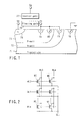
A flash memory is provided as one type of a
semiconductor memory device. FIG. 1 shows the cross
sectional construction of one memory cell element of
the flash memory. In FIG. 1, an N-type well region
(N-well) 72 is formed in a P-type semiconductor
substrate (P-substrate) 71. Further, a P-type
well region (P-well) 73 is formed in the N-type well
region 72. In the P-type well region 73, source and
drain regions 74, 75 of a memory cell which are formed
of n+-type regions are separately formed. A floating
gate electrode 76 is formed above the channel region
between the source and drain regions 74 and 75 with
an insulating film disposed therebetween and a control
gate electrode 77 is formed above the floating gate
electrode 76 with an insulating film disposed
therebetween.
-
Further, a contact region 78 formed of a p+-type
region is formed on the P-substrate 71, a contact
region 79 formed of an n+-type region is formed on
the N-type well region 72 and a contact region 80
formed of a p+-type region is formed on the P-type well
region 73.
-
At the operating time, gate voltage Vg, drain
voltage Vd and source voltage Vs are respectively
applied to the control gate electrode 77, drain region
75 and source region 74. Further, the same voltage as
the source voltage Vs is applied to the contact regions
79 and 80 and a ground voltage of 0V is applied to the
contact region 78.
-
The above memory cell stores data of "1" or "0"
level according to the amount of electrons accumulated
in the floating gate electrode 76. The threshold
voltage as viewed from the control gate electrode 77 is
changed according to the level of the stored data.
-
A memory cell array is constructed by use of
a plurality of memory cells which have the same
construction as the above memory cell. FIG. 2 shows
an example of a circuit of the memory cell array of
a NOR type flash memory. A plurality of memory cells
MC are arranged in a matrix form and the control gate
electrodes of the memory cells MC arranged on the same
row are commonly connected to a corresponding one of
a plurality of word lines WL0 to WLn. Further, the
drains of the memory cells MC arranged on the same
column are commonly connected to a corresponding one of
a plurality of bit lines BL0 to BLm. Generally, the
memory cells are divided into a plurality of blocks and
the sources of the memory cells MC in the same block
are commonly connected to a corresponding one of
a plurality of source lines SLi which is provided for
the block.
-
FIG. 3 shows the relation between the gate voltage
(Vg) applied to the control gate electrode and a drain
current flowing in the memory cell at the operating
time. In this example, the state in which the amount
of electrons accumulated in the floating gate electrode
is relatively large, that is, the state in which the
threshold voltage Vt of the memory cell is high is
defined as "0" data (the memory cell storing "0" data
is referred to as a "0" cell) and the state in which
the amount of accumulated electrons is relatively
small, that is, the state in which the threshold
voltage Vt of the memory cell is low is defined as "1"
data (the memory cell storing "1" data is referred to
as a "1" cell).
-
One example of the voltage bias condition at the
data readout time, program time and erase time is shown
in the following table 1.
| | Readout | Program | Erase |
| Vg | 5V | | 9V | -7V |
| Vd | 1V |
| | 5V("1") | Floating |
| 0V("0") |
| Vs | 0V | 0V | | 10V |
-
That is, the table 1 shows one example of values
of the voltages Vg, Vd, Vs supplied to the memory cell.
At the data readout time, Vg, Vd, Vs are respectively
set at 5V, 1V, 0V. At the data program time, Vg, Vs
are respectively set at 9V, 0V and Vd is set at 5V for
the memory cell into which data is programmed and at 0V
for the other memory cells (in which original "1" data
is kept). Further, at the data erase time, Vg, Vs are
respectively set at -7V, 10V and Vd is set in the
electrically floating state.
-
Readout data is determined according to whether a
cell current flows or not when voltage Vread (in this
example, 5V) is applied to the control gate electrode
while preset voltage (in this example, 1V) is being
applied to the drain. The above determination is made
by comparing the cell current with a reference current
(Iref) flowing in a reference cell by use of a sense
amplifier (not shown).
-
The erase operation is simultaneously effected
for a plurality of memory cells which commonly have
the P-well 73 (shown in FIG. 1). At the erase time,
all of the memory cells subjected to the erase process
are set into "1" cells by causing electrons to flow
from the floating gate electrodes 76 thereof into the
P-type well region 73 according to the Fowler-Nordheim
(F·N) tunneling phenomenon.
-
The program operation is effected for each memory
cell. The bit line connected to the memory cell in
which "0" data is programmed is biased to 5V so as to
inject electrons of high energy generated by the
channel hot electron phenomenon into the floating gate
electrode 76 of the memory cell. The bit line
connected to the "1" cells in which original "1" data
is maintained is set at 0V. As a result, no electrons
are injected into the floating gate electrode 76 and
the threshold voltage Vt is kept unchanged in the
non-programmed memory cell.
-
Further, in the flash memory, the program verify
operation and erase verify operation are effected at
the program time and erase time to confirm the extent
to which data is programmed and erased. In the program
verify operation, the "0" readout operation is effected
by setting the voltage of the control gate electrode at
high voltage Vpv (for example, 7V) in comparison with
the voltage Vread (in this example, 5V) set at the
readout time. Then, the program operations and program
verify operations are repeatedly and alternately
effected and the program operation is terminated when
data items of the memory cells to be programmed are all
set to "0".
-
At the erase time, the "1" readout operation is
effected by setting the voltage of the control gate
electrode 77 at low voltage Vev (for example, 3.5V) in
comparison with the voltage Vread set at the readout
time. Then, the erase operations and erase verify
operations are repeatedly and alternately effected and
the erase operation is terminated when data items of
the memory cells subjected to the erase process are all
set to "1". As a result, a sufficiently large cell
current Icell can be attained.
-
Thus, the voltage applied to the control gate
electrode of the memory cell is set to various values
such as 9V, 7V, 5V, 3.5V according to the various
operation modes. Among the above voltages, 9V, 7V, 5V
are higher than the power supply voltage supplied from
the exterior.
-
Conventionally, in order to generate various
voltages such as 9V, 7V, 5V which are higher than
the power supply voltage supplied from the exterior,
a required number of booster circuits for boosting
the power supply voltage are provided and one of
the outputs of the plurality of booster circuits is
adequately selected by use of a switch and the selected
output is applied to the control gate electrode of
the memory cell.
-
However, since the booster circuit necessitates
elements such as capacitors which occupy a large area
on the chip, there occurs a problem that the chip area
becomes large if a plurality of booster circuits are
provided. Further, since the consumption current in
the booster circuit is relatively large, a problem that
the consumption current in the whole portion of the
chip becomes large occurs.
-
As described above, since a plurality of booster
circuits are provided in the conventional semiconductor
memory device which requires various voltages higher
than the power supply voltage supplied from the
exterior, problems that the chip area becomes large at
the time of integrating the device and the consumption
current becomes large occur.
-
Accordingly, an object of this invention is to
provide a boosted voltage generating circuit capable of
generating various voltages higher than the power
supply voltage supplied from the exterior without
making the chip area larger at the time of integration
and increasing the consumption current.
-
Further, another object of this invention is to
provide a semiconductor memory device capable of
generating various voltages higher than the power
supply voltage supplied from the exterior without
making the chip area larger at the time of integration
and increasing the consumption current.
-
According to this invention, there is provided a
boosted voltage generating circuit comprising a first
voltage output circuit for receiving first voltage and
outputting second voltage obtained by boosting the
first voltage; a second voltage output circuit coupled
with the first voltage output circuit, for generating
third voltage whose voltage value is smaller than
the value of the second voltage and which is variably
set to at least two values based on the second voltage;
and a equalizer circuit coupled with the first and
second voltage output circuits, for short-circuiting
an output node of the second voltage and an output
node of the third voltage in response to a first
control signal.
-
Further, according to this invention, there is
provided a semiconductor memory device comprising a
memory cell array having a plurality of data-erasable
memory cells having gate electrodes, for storing data;
a plurality of word lines coupled with the gate
electrodes of the plurality of memory cells; a first
voltage output circuit for receiving first voltage and
outputting second voltage obtained by boosting the
first voltage; a second voltage output circuit coupled
with the first voltage output circuit, for generating
third voltage whose voltage value is smaller than
the value of the second voltage and which is variably
set to at least two values based on the second voltage;
a equalizer circuit coupled with the first and second
voltage output circuits, for short-circuiting an output
node of the second voltage and an output node of
the third voltage in response to a first control
signal; and a row decoder circuit coupled with the
second voltage output circuit, for setting potentials
of the plurality of word lines based on the third
voltage.
-
This summary of the invention does not necessarily
describe all necessary features so that the invention
may also be a sub-combination of these described
features.
-
The invention can be more fully understood from
the following detailed description when taken in
conjunction with the accompanying drawings, in which:
- FIG. 1 is a view showing the cross sectional
structure of one memory cell in a flash memory;
- FIG. 2 is a diagram showing an example of the
circuit of a memory cell array of a NOR type flash
memory;
- FIG. 3 is a characteristic diagram showing the
relation between gate voltage applied to the control
gate electrode of a memory cell and a drain current of
the memory cell;
- FIG. 4 is a block diagram showing a general
boosted voltage generating circuit;
- FIG. 5 is a timing chart showing one example of
the operation of the circuit shown in FIG. 4;
- FIG. 6 is a block diagram showing a boosted
voltage generating circuit according to a first
embodiment of this invention;
- FIG. 7 is a timing chart for illustrating one
example of the operation of the circuit shown in
FIG. 6;
- FIG. 8 is a circuit diagram showing one example of
the concrete construction of a booster circuit shown in
FIG. 6;
- FIG. 9 is a circuit diagram showing one example of
the concrete construction of a regulator circuit shown
in FIG. 6;
- FIG. 10 is a circuit diagram showing one example
of the concrete construction of a comparator shown in
FIG. 9;
- FIG. 11 is a circuit diagram showing one example
of the concrete construction of a equalizer circuit
shown in FIG. 6;
- FIG. 12 is a timing chart for illustrating one
example of the operation which is different from the
operation shown in FIG. 7;
- FIG. 13 is a circuit diagram showing the concrete
construction of the regulator circuit shown in FIG. 6
according to a modification of the first embodiment of
this invention together with another circuit including
a control signal generating circuit;
- FIG. 14 is a timing chart for illustrating one
example of the operation of the circuit shown in
FIG. 13;
- FIG. 15 is a block diagram showing a boosted
voltage generating circuit according to a second
embodiment of this invention;
- FIG. 16 is a block diagram showing the whole
construction of a memory formed when this invention is
applied to a flash memory;
- FIG. 17 is a waveform diagram showing the relation
between the word line voltage and a equalizing control
signal EQLE in the memory shown in FIG. 16;
- FIG. 18 is a diagram showing the state of
distribution of the threshold voltage of the memory
cell after data erasing;
- FIG. 19 is a cross sectional view showing the
structure of part of the flash memory shown in FIG. 16;
and
- FIG. 20 is a timing chart at the time of erase
operation of the flash memory shown in FIG. 16.
-
-
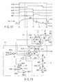
FIG. 4 shows the construction of a boosted voltage
generating circuit of a semiconductor memory device
disclosed in Jpn. Pat. Appln. KOKAI Publication
No. 10-11987 in a block form. For example, the circuit
shown in FIG. 4 is contained in a flash memory to
generate various voltages applied to the control gate
of the memory cell in various operation modes as
described before. The boosted voltage generating
circuit includes a booster circuit 11 and regulator
circuit 12.
-
The booster circuit 11 is operated when a booster
activation signal VPPE is activated and boosts power
supply voltage Vcc supplied from the exterior to output
voltage Vpp having a value larger than the power supply
voltage. The voltage Vpp is supplied to the regulator
circuit 12.
-
The regulator circuit 12 outputs voltage Vreg
whose voltage value is smaller than Vpp and which is
variably set to a plurality of values based on the
voltage Vpp. The operation of the regulator circuit 12
is controlled according to a regulator activation
signal REGE, a programming signal PROG activated at
the program operation time of the memory cell, and
a verifying signal VRFY activated at the program verify
operation time of the memory cell.
-
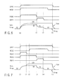
Next, one example of the operation of the circuit
of FIG. 4 is explained with reference to the timing
chart of FIG. 5. Before time t0 in FIG. 5, it is
assumed that both of the voltages Vpp and Vreg are set
at the readout voltage of 5V, for example.
-
If the booster activation signal VPPE is activated
at time t0, the booster circuit 11 starts the operation
to start the boosting operation of the power supply
voltage Vcc supplied from the exterior. After this,
the voltage Vpp rises.
-
When the operation of the booster circuit 11
becomes stable, the voltage Vpp reaches a specified
value and becomes stable. The specified value of the
voltage Vpp is set at 10V, for example, and it is the
same as the source voltage Vs applied to the source
region when the erase process is effected in the memory
cell. The voltage Vpp of 10V can be used as the source
voltage Vs applied to the source region at the time of
erase operation.
-
The regulator activation signal REGE is activated
at time t0, and at the same time, the programming
signal PROG is activated. As a result, the regulator
circuit 12 is operated and the voltage Vreg rises
towards a value of 9V, for example, which is lower than
the voltage Vpp and becomes stable after it has reached
9V. The voltage of 9V output as the voltage Vreg while
the signal FROG is kept at the "H" level is used as the
voltage Vg applied to the control gate electrode of the
memory cell at the time of erase operation.
-
Next, the programming signal PROG is deactivated
at time t1 and the verifying signal VRFY is activated.
As a result, the output voltage Vreg of the regulator
circuit 12 starts to be lowered from 9V to 7V and
becomes stable after it has reached 7V. The voltage of
7V output as the voltage Vreg while the signal VRFY is
kept at the "H" level is used as the voltage Vpv
applied to the control gate electrode of the memory
cell at the time of program verify operation.
-
When the verifying signal VRFY is deactivated at
time t2, the output voltage Vreg of the regulator
circuit 12 starts to be lowered from 7V towards 5V at
which the voltage was initially set. Further, when
the booster activation signal VPPE is deactivated at
time t3, the operation of the booster circuit 11 is
terminated and the voltage Vpp starts to be lowered
towards 5V at which the voltage was initially set.
-
Thus, in the boosted voltage generating circuit of
FIG. 4, the voltages with different values applied to
the control gate electrode of the memory cell in
the various operation modes of the memory cell are
generated by using the voltage Vpp output from
the booster circuit 11 and sequentially changing
the value of the voltage Vpp by use of the regulator
circuit 12. Therefore, it is unnecessary to provide
booster circuits of the number corresponding to the
number of different levels of the voltages generated.
Thus, the occupancy area in the chip occupied by the
booster circuit at the time of integration can be made
small and a consumption current can be reduced.
-
However, with the boosted voltage generating
circuit of FIG. 4, the magnitude of a current flowing
between the node of the voltage Vpp and the ground
voltage node in the regulator circuit 12 immediately
after the program operation is started becomes large,
thereby causing the rise of the voltage Vpp and the
rise of the voltage Vreg to be delayed in some cases.
-
Therefore, in the boosted voltage generating
circuit according to this invention, attention is paid
to eliminate the delay of the rise of the voltage Vpp,
Vreg.
-
FIG. 6 is a block diagram of a boosted voltage
generating circuit according to a first embodiment of
this invention. The boosted voltage generating circuit
is contained in a flash memory and generates various
voltages applied to the control gate electrode of the
memory cell in various operation modes.
-
Like the boosted voltage generating circuit shown
in FIG. 4, the above boosted voltage generating circuit
includes a booster circuit 11 and regulator circuit 12
and further includes a equalizer circuit 13. The
booster circuit 11 and regulator circuit 12 have the
same construction and function as those of the booster
circuit 11 and regulator circuit 12 shown in FIG. 4,
and therefore, the explanation thereof is omitted. The
equalizer circuit 13 which is newly provided is
connected to the booster circuit 11 and regulator
circuit 12, the operation thereof is controlled by
a equalizing control signal EQLE and the node of the
voltage Vpp and the node of the voltage Vreg are short-circuited
by the equalizer circuit 13 when the signal
EQLE is activated ("H" level).
-
Next, one example of the operation of the circuit
shown in FIG. 6 is explained with reference to the
timing chart of FIG. 7. Also, in this case, it is
assumed that both of the voltages Vpp and Vreg are set
at the readout voltage of 5V, for example, before time
t0 in FIG. 7.
-
If the booster activation signal VPPE is activated
at time t0, the booster circuit 11 starts the operation
and the voltage Vpp starts to rise. At the same time,
the equalizing control signal EQLE is activated and the
node of the voltage Vpp and the node of the voltage
Vreg are short-circuited by the equalizer circuit 13.
As a result, the voltage Vreg rises in the same manner
as the voltage Vpp.
-
Next, when the equalizing control signal EQLE is
set to the "L" level at time t1, the short-circuiting
state set by the equalizer circuit 13 is released.
After this, the output voltage Vpp of the booster
circuit 11 reaches a specified value and becomes
stable. The specified value of the voltage Vpp is set
at 10V, for example, and it is the same as the source
voltage Vs applied to the source region when the erase
process is effected in the memory cell. The voltage of
10V obtained at this time can be used as the source
voltage Vs applied to the source region at the time of
erase operation.
-
The regulator activation signal REGE is activated
at time t2 which comes after the voltage Vreg rises to
some extent. The programming signal PROG is activated
at the same time as activation of the booster
activation signal VPPE. The regulator circuit 12 is
operated by activation of the signal REGE and the
voltage Vreg is controlled and set to 9V, for example,
which is lower than the voltage Vpp.
-
Next, the programming signal PROG is deactivated
at time t3 and the verifying signal VRFY is activated.
As a result, the output voltage Vreg of the regulator
circuit 12 starts to be lowered from 9V to 7V and
becomes stable after it has reached 7V.
-
When the verifying signal VRFY is deactivated at
time t4, the output voltage Vreg of the regulator
circuit 12 starts to be lowered from 7V towards 5V.
Further, when the booster activation signal VPPE is
deactivated at time t5, the operation of the booster
circuit 11 is terminated and the voltage Vpp starts to
be lowered towards 5V at which the voltage was
initially set.
-
FIG. 8 shows one example of the concrete circuit
construction of the booster circuit 11 of FIG. 6. The
booster circuit 11 includes an oscillator 21, charge
pump 22 and voltage detector 23.
-
The oscillator 21 includes a negative feedback
circuit having a NAND gate NA1 and two inverters IV1,
IV2, the operation of the negative feedback circuit is
controlled according to an oscillator activation signal
OSCE output from the voltage detector 23 and the
oscillator oscillates at a preset frequency when the
negative feedback circuit is operated.
-
The charge pump 22 includes three I-type
(intrinsic type: the threshold voltage thereof is
approximately 0V) MOS transistors QI1 to QI3 whose
source-drain paths are serially connected between
the supply node of the power supply voltage Vcc and
the output node of the voltage Vpp, a capacitor C1
connected between the series connection node of
the transistors QI1 and QI2 and the output node of
the inverter IV2 of the oscillator 21, and a capacitor
C2 connected between the series connection node of
the transistors QI2 and QI3 and the output node of
the inverter IV1 of the oscillator 21.
-
The oscillator activation signal OSCE output from
the voltage detector 23 is supplied to the gate of the
transistor QI1 which is disposed in a position closest
to the supply node of the power supply voltage Vcc and
the gates of the other transistors QI2, QI3 are
respectively connected to their own sources or one-side
ends of the capacitors C1, C2.
-
The voltage detector 23 includes an inverter IV3
supplied with the booster activation signal VPPE,
an inverter IV4 supplied with an output signal of
the inverter IV3, a level shift circuit 24 which has
P-channel MOS transistors QP1, QP2 and N-channel MOS
transistors QN1, QN2 and in which the outputs of
the inverters IV3, IV4 are respectively supplied to
the gates of the N-channel MOS transistors QN1, QN2,
a P-channel MOS transistor QP3 whose gate is supplied
with an output of the shift circuit 24 and which is
connected at one end of the source-drain path to the
output node of the voltage Vpp, two voltage dividing
resistors R1, R2 serially connected between the other
end of the source-drain path of the transistor QP3 and
the supply node of the ground voltage and a comparator
25 for comparing a divided voltage Vdiv obtained by use
of the resistors R1, R2 with reference voltage Vref and
generating the oscillator activation signal OSCE.
-
In the booster circuit 11, when the booster
activation signal VPPE is set to the "H" level, the
output of the inverter IV3 of the voltage detector 23
is set to the "L" level, the output of the inverter IV4
is set to the "H" level, and the output of the level
shift circuit 24 is set to the "L" level. Then, the
P-channel MOS transistor QP3 is turned ON and the
voltage Vpp is divided by the two resistors R1, R2.
The divided voltage Vdiv thus obtained is compared with
the reference voltage Vref by the comparator 25.
-
Since the voltage Vpp is low immediately after
the booster circuit 11 is operated, the relation of
Vref > Vdiv is set up and the oscillator activation
signal OSCE which is the output of the comparator 25 is
set at the "H" level. When the oscillator activation
signal OSCE is set at the "H" level, the oscillator 21
oscillates at a preset frequency. Further, when the
signal OSCE is set at the "H" level, the transistor QI1
of the charge pump 22 is turned ON and the oscillation
signal of the oscillator 21 is supplied to the sources
of the transistors QI2, QI3 of the charge pump 22 via
the capacitors C1, C2. Therefore, positive charges are
sequentially transferred to the output node of Vpp to
sequentially raise the voltage value of Vpp.
-
When the voltage Vpp rises and exceeds the
specified value, the relation of Vref < Vdiv is set up
and the oscillator activation signal OSCE is set at
the "L" level. As a result, the oscillation operation
of the oscillator 21 is interrupted and the charge
transfer operation by the charge pump 22 is also
interrupted. If the voltage Vpp is lowered and becomes
lower than the specified value in this state, the
oscillator activation signal OSCE is set at the "H"
level again, the oscillation operation is started
again and the charge transfer operation by the charge
pump 22 is started again. The above operations are
repeatedly effected in a period in which the booster
activation signal VPPE is kept at the "H" level and
the boosted voltage is output from the output node of
the voltage Vpp.
-
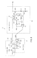
FIG. 9 shows one example of the concrete circuit
construction of the regulator circuit 12 of FIG. 6.
The regulator circuit 12 includes two comparators 26,
27 whose activation states are controlled by a
regulator activation signal REGE, a P-channel MOS
transistor QP4 having a source connected to the supply
node of the voltage Vpp and a gate electrode connected
to the drain thereof, a P-channel MOS transistor QP5
having a source connected to the supply node of
the voltage Vpp, a gate electrode commonly connected to
the gate of the transistor QP4 and a drain connected to
the output node of the voltage Vreg and constituting
a current mirror circuit in cooperation with the
transistor QP4, an N-channel MOS transistor QN3 having
a drain connected to the drain of the transistor QP4,
a source connected to the ground voltage node and
a gate electrode supplied with an output of the
comparator 26, an N-channel MOS transistor QN4 having
a drain connected to the drain of the transistor QP5,
a source connected to the ground voltage node and
a gate electrode supplied with an output of the
comparator 27, three voltage-dividing resistors R3, R4,
R5 serially connected between the output node of the
voltage Vreg and the ground voltage node, an N-channel
MOS transistor QN5 having a source-drain path connected
between the resistor R5 among the three resistors R3,
R4, R5 which is disposed in a position closest to the
ground voltage node and the ground voltage node and
a gate electrode supplied with a verifying signal VRFY,
and an N-channel MOS transistor QN6 having a source-drain
path connected between the series connection node
of the resistors R4 and R5 among the three resistors
R3, R4, R5 and the ground voltage node and a gate
electrode supplied with a programming signal PROG.
-
The reference voltage Vref is supplied to the
non-inverting input terminal (+) of the comparator 26
and the inverting input terminal (-) of the comparator
27 and the divided voltage at the series connection
node of the two resistors R3, R4 is supplied to
the inverting input terminal (-) of the comparator 26
and the non-inverting input terminal (+) of the
comparator 27. The comparators 26, 27 are operated
to compare the input voltages when the regulator
activation signal REGE is set at the "H" level.
-
In the regulator circuit 12, the regulator
activation signal REGE is set at the "L" level in
a period between times t0 and t1 shown in FIG. 7, the
two comparators 26, 27 are set in the deactivated state
and neither of them are operated.
-
If the regulator activation signal REGE is set at
the "H" level at time t2 in FIG. 7, the two comparators
26, 27 are activated and both set into the operative
state. If the programming signal PROG is set to the
"H" level at time t0 earlier than t1, the transistor
QN6 is turned ON, the voltage Vreg is divided by
the two resistors R3 and R4 and the divided
voltage obtained at this time is input to the
comparators 26, 27.
-
In this case, the node of the voltage Vreg is
connected to the supply node of the voltage Vpp by the
equalizer circuit 13, the voltage Vreg is sufficiently
raised, the divided voltage obtained by dividing
the voltage Vreg by use of the two resistors R3, R4
becomes higher than the voltage Vref, the output of
the comparator 26 is set to the "L" level and the
output of the comparator 27 is set to the "H" level.
As a result, the transistor QN4 is turned ON and the
transistor QN3 is turned OFF, the node of the voltage
Vreg is discharged towards the potential of the ground
voltage node via the transistor QN4 and thus the
voltage Vreg starts to be lowered.
-
When the voltage Vreg is lowered and becomes lower
than 9V which is set as the specified value, the
divided voltage at the series connection node of the
resistors R3 and R4 becomes lower than the reference
voltage Vref, and as a result, the output of the
comparator 26 is inverted from the "L" level to the "H"
level and the output of the comparator 27 is inverted
from the "H" level to the "L" level. At this time,
the transistor QN3 is turned ON and the transistor QN4
is turned OFF and a current I1 shown in FIG. 9
flows from the node of the voltage Vpp towards the
ground voltage node via the transistors QP4 and QN3.
By causing the current I1 to flow, a current I2 shown
in FIG. 9 flows from the node of the voltage Vpp
(the specified value is 10V) towards the node of
the voltage Vreg via the transistor QP5 so as to charge
the node of the voltage Vreg. As a result, the voltage
Vreg which has become lower than 9V starts to rise.
-
Thus, the divided voltage at the series connection
node of the resistors R3 and R4 and the reference
voltage Vref are compared with each other by the
comparators 26, 27, the ON/OFF states of the N-channel
MOS transistors QN3, QN4 are controlled according to
the result of comparison and the voltage Vreg is
controlled so as to be always set equal to the
specified value (9V) at the program time by
charging/discharging the node of the voltage Vreg.
-
In a period between times t3 and t4 of FIG. 7 in
which the programming signal PROG is set at the "L"
level and the verifying signal VRFY is set at the "H"
level, the transistor QN6 is turned OFF and the
transistor QN5 is turned ON, and therefore, the voltage
Vreg is divided by the three resistors R3, R4. R5 and
the divided voltage obtained based on the resistance
dividing ratio which is smaller than that at the
program time is input to the comparators 26, 27. In
this case, the resistances of the resistors R3, R4, R5
are so set that the divided voltage obtained when the
voltage Vreg reaches 7V which is lower than 9V set as
the specified value will become equal to the divided
voltage obtained when the voltage Vreg is set at 9V.
-
Therefore, at the time of verify, the divided
voltage generated at the series node of the resistors
R3 and R4 is compared with the reference voltage Vref
by the comparators 26, 27, the ON/OFF states of the
N-channel MOS transistors QN3, QN4 are controlled
according to the result of comparison, and the voltage
Vreg is controlled so as to be always set equal to
the specified value (7V) at the time of verify by
charging/discharging the node of the voltage Vreg.
-
FIG. 10 shows one example of the concrete circuit
construction of the comparators 26, 27 shown in FIG. 6.
The source of a P-channel MOS transistor QP6 is
connected to the supply node of the power supply
voltage Vcc. The sources of two P-channel MOS
transistors QP7, QP8 are connected to the drain of the
transistor QP6. The gate electrodes of the transistors
QP7, QP8 are connected together and the drain of the
transistor QP8 is connected to the common connection
node of the gate electrodes. The drain of the
transistor QP7 is connected to the drain of an
N-channel MOS transistor QN7. The gate electrode of
the transistor QN7 is used as the inverting input
terminal (-). The drain of the transistor QP8 is
connected to the drain of an N-channel MOS transistor
QN8. The gate electrode of the transistor QN8 is used
as the non-inverting input terminal (+). The sources
of the transistors QN7, QN8 are connected together and
a current source 28 is connected between the source
common connection node and the ground voltage node.
That is, the transistors QP6, QP7, QP8, QN7, QN8 and
current source 28 are combined to constitute a current
mirror load type differential amplifier.
-
The regulator activation signal REGE is input to
an inverter 29 and the output of the inverter 29 is
input to the gate electrode of the P-channel MOS
transistor QP6. Further, the output of the inverter 29
is input to the gate electrode of an N-channel MOS
transistor QN9. The source of the MOS transistor QN9
is connected to the output node OUT of the differential
amplifier which is the drain common connection node of
the P-channel MOS transistor QP7 and N-channel MOS
transistor QN6 and the drain thereof is connected to
the ground voltage node.
-
When the regulator activation signal REGE is set
at the "L" level in the comparator 26 (27), the output
of the inverter 29 is set to the "H" level to turn OFF
the P-channel MOS transistor QP6 and turn ON the
N-channel MOS transistor QN9. At this time, the
differential amplifier is not operated, the output node
OUT is connected to the ground voltage node via the
transistor QN9 and a signal of the output node OUT is
set to the "L" level irrespective of the voltages input
to the inverting input terminal (-) and onon-inverting
input terminal (+).
-
When the regulator activation signal REGE is set
at the "H" level, the output of the inverter 29 is
set to the "L" level to turn ON the P-channel MOS
transistor QP6 and the differential amplifier is set
into the operative state so that the voltages input to
the inverting input terminal (-) and non-inverting
input terminal (+) can be compared with each other by
the differential amplifier. At this time, if the
voltage input to the non-inverting input terminal (+)
is higher than the voltage input to the inverting input
terminal (-), the N-channel MOS transistor QN8 is
turned ON and the signal of the output node OUT is set
to the "H" level. On the other hand, if the voltage
input to the non-inverting input terminal (+) is lower
than the voltage input to the inverting input terminal
(-), the N-channel MOS transistor QN7 is turned ON and
the signal of the output node OUT is set to the "L"
level.
-
FIG. 11 shows one example of the concrete circuit
construction of the equalizer circuit 13 in FIG. 6.
The equalizer circuit 13 includes an inverter IV5
supplied with a equalizing control signal EQLE, an
inverter IV6 supplied with an output of the inverter
IV5, a level shift circuit 30 which has P-channel MOS
transistors QP9, QP10 and N-channel MOS transistors
QN10, QN11 and in which the outputs of the inverters
IV5, IV6 are input to the gates of the N-channel MOS
transistors QN10, QN11, and a P-channel MOS transistor
QP11 having a gate electrode supplied with an output of
the level shift circuit 30, a source connected to the
output node of the voltage Vpp and a drain connected to
the output node of the voltage Vreg.
-
In the equalizer circuit 13, when the equalizing
control signal EQLE is set at the "H" level, the output
of the inverter IV5 is set at the "L" level and the
output of the inverter IV6 is set at the "H" level so
that the transistors QN10 will be turned OFF, the
transistor QN11 will be turned ON and the output of the
level shift circuit 30 will be set at the "L" level.
As a result, the transistor QP11 is turned ON to short-circuit
the node of the voltage Vpp and the node of the
voltage Vreg.
-
On the other hand, when the equalizing control
signal EQLE is set at the "L" level, the output of the
inverter IV5 is set at the "H" level and the output of
the inverter IV6 is set at the "L" level so that the
transistors QN10 will be turned ON, the transistor QN11
will be turned OFF and the output of the level shift
circuit 30 will be set at the "H" level (Vpp). As a
result, the transistor QP11 is turned OFF to separate
the node of the voltage Vpp and the node of the voltage
Vreg from each other.
-
Thus, like the boosted voltage generating circuit
of FIG. 4, in the boosted voltage generating circuit of
FIG. 6, voltages of different values applied to the
control gate electrode of the memory cell in various
operation modes of the memory cell are generated by
using the voltage Vpp output from the booster circuit
11 and variously setting the value of the voltage Vpp
by use of the regulator circuit 12, the following
effect can be obtained in addition to the same effect
obtained in the circuit of FIG. 4.
-
In the circuit of this embodiment shown in FIG. 6,
the regulator circuit 12 is kept inoperative
immediately after the boosting operation of the booster
circuit 11 is started and the equalizer circuit 13 is
operated instead so as to short-circuit the node of the
voltage Vpp and the node of the voltage Vreg. That is,
as shown in FIG. 7, the operation period of the
regulator circuit 12 and the short-circuiting operation
period of the equalizer circuit 13 do not overlap each
other. Therefore, a large current (current I1 in
FIG. 9) which flowed into the ground voltage node at
the rise time of the voltage Vpp does not flow so that
the voltage Vpp and voltage Vreg can rise at higher
speed. Further, since a large current which flowed
into the ground voltage node immediately after the
boosting operation of the booster circuit 11 is started
does not flow, the consumption current can be
significantly reduced in comparison with that in
the case of FIG. 4.
-
In the above explanation for the operation of
the embodiment, a case wherein the operative period of
the regulator circuit 12 and the short-circuiting
operation period of the equalizer circuit 13 do not
overlap each other as shown in the timing chart of
FIG. 7 is explained, but as shown in the timing chart
of FIG. 12, the timing at which the equalizing control
signal EQLE falls to the "L" level can be delayed to
the timing at which the programming signal PROG falls
to the "L" level (t3 in FIG. 12). In this case, the
operative period of the regulator circuit 12 and the
short-circuiting operation period of the equalizer
circuit 13 partly overlap each other.
-
Thus, by setting the period in which the
equalizing control signal EQLE is activated equal to
the period in which the programming signal PROG is
activated, the voltage of the control gate of the
memory cell at the program time and the well voltage at
the erase time can be set equal to each other when the
voltage Vpp is supplied to the well region.
-
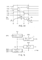
Next, a modification of the first embodiment is
explained below. FIG. 13 shows another example of the
concrete circuit construction of the regulator circuit
12 of FIG. 6 together with a control circuit such as a
control signal generating circuit for generating the
regulator activation signal REGE and equalizing control
signal EQLE.
-
The regulator circuit 12 shown in FIG. 13 is
different from that of FIG. 9 in that the activating
operation of the comparator 27 is not controlled by the
regulator activation signal REGE but by another control
signal generated by a signal generating circuit which
will be described later.
-
A control signal generating circuit 31 generates
the regulator activation signal REGE, equalizing
control signal EQLE and the like according to the
programming signal PROG, verifying signal VRFY and
the like. The circuit 31 includes a comparator 32 for
comparing the reference voltage Vref with a divided
voltage at the series connection node of the resistors
R3 and R4 in the regulator circuit 12, an inverter 33
supplied with the booster activation signal VPPE, two
NOR gates NOR1, NOR2 whose one-side input terminals
are respectively supplied with the outputs of the
comparator 32 and the inverter 33, the other input
terminals and output terminals thereof being crosscoupled
to constitute a latch circuit 34, a NOR gate
NOR3 supplied with the output of the NOR gate NOR2 and
the output of the inverter 33, a NOR gate NOR4 supplied
with the programming signal PROG and verifying signal
VRFY, and an inverter 35 supplied with the output of
the NOR gate NOR4.
-
The regulator activation signal REGE is generated
from the NOR gate NOR2. The regulator activation
signal REGE is input to the comparator 26 in the
regulator circuit 12. The equalizing control signal
EQLE is generated from the NOR gate NOR3 and input
to the equalizer circuit 13 shown in FIG. 6. Further,
the output of the inverter 35 is input as an activation
signal to the comparator 27 in the regulator
circuit 12.
-
A voltage setting circuit 36 sets the node of the
voltage Vreg and the node of the voltage Vpp to boosted
voltage, for example, 5V before the boosting operation
of the booster circuit 11 is started and after the
boosting operation is terminated. The circuit 36
includes an inverter IV7 supplied with the output of
the inverter 35 in the control signal generating
circuit 31, a level shift circuit 37 which has
P-channel MOS transistors QP12, QP13 and N-channel MOS
transistors QN12, QN13 and in which the outputs of the
inverters 35 and IV7 are supplied to the gates of the
N-channel MOS transistors QN12, QN13, a P-channel MOS
transistor QP14 having a gate electrode supplied with
the output of the level shift circuit 37, a source
connected to the 5V supply node and a drain connected
to the node of the voltage Vreg, and a P-channel MOS
transistor QP15 having a source connected to the 5V
supply node and a drain connected to the node of the
voltage Vpp.
-
Next, one example of the operation of the circuit
shown in FIG. 13 is explained with reference to the
timing chart of FIG. 14. First, since the programming
signal PROG and verifying signal VRFY are both set at
the "L" level before time t0, the output of the NOR
gate NOR4 in the signal generating circuit 31 is set
at the "H" level and the output of the inverter 35
supplied with the output of the NOR gate NOR4 is set at
the "L" level. Further, the output of the inverter IV7
of the voltage setting circuit 36 which is supplied
with the output of the inverter 35 is set at the "H"
level. At this time, the N-channel MOS transistors
QN12 and QN13 of the level shift circuit 37 in the
voltage setting circuit 36 are respectively turned OFF
and ON and the output of the level shift circuit 37 is
set to the "L" level. As a result, the two P-channel
MOS transistors QP14, QP15 whose gates are supplied
with the output of the level shift circuit 37 are
turned ON so as to permit a voltage of 5V to be
supplied to the node of the voltage Vreg and the node
of the voltage Vpp, and thus the voltages Vreg and Vpp
are both set at 5V.
-
If the booster activation signal VPPE is activated
("H" level) at time t0, the booster circuit 11 starts
the boosting operation and the voltage Vpp starts to
rise. Further, when the signal VPPE is set at the "H"
level, the output of the inverter 33 in the signal
generating circuit 31 is set to the "L" level.
Assuming now that the regulator activation signal REGE
which is the output of the NOR gate NOR2 constructing
the latch circuit 34 is previously set at the "L"
level, the equalizing control signal EQLE which is the
output of the NOR gate NOR3 is set at the "H" level.
As described before, the transistor QP11 of the
equalizer circuit 13 of FIG. 11 is turned ON in
response to the signal EQLE to short-circuit the node
of the voltage Vpp and the node of the voltage Vreg.
-
When the programming signal PROG is set at the "H"
level at time t0, the output of the NOR gate NOR4 in
the signal generating circuit 31 is inverted to the "L"
level and the output of the inverter 35 is inverted to
the "H" level so that the N-channel MOS transistors
QN12 and QN13 of the level shift circuit 37 in the
voltage setting circuit 36 will be respectively turned
ON and OFF and the output of the level shift circuit 37
will be inverted to the "H" level. As a result, the
two P-channel MOS transistors QP14, QP15 whose gate
electrodes are supplied with the output of the level
shift circuit 37 are turned OFF so as to separate the
nodes of the voltages Vreg and Vpp from the 5V supply
node. Therefore, the voltage vreg and the output
voltage Vpp of the booster circuit 11 gradually rise.
-
The output voltage Vreg of the regulator circuit
12 rises as the output voltage Vpp of the booster
circuit 11 rises, and if the voltage Vreg reaches a
specified value (9V) at time t1 and the divided voltage
obtained by use of the two resistors R3, R4 in the
regulator circuit 12 exceeds the reference voltage Vref
as described before, the output of the comparator 32 of
the control signal generating circuit 31 is set to the
"H" level, and as a result, the regulator activation
signal REGE which is the output of the NOR gate NOR2
of the latch circuit 34 is inverted from the "L" level
to the "H" level and the comparator 26 in the regulator
circuit 12 is activated. At this time, since
the programming signal PROG is set at the "H" level,
the output of the NOR gate NOR4 of the signal
generating circuit 31 is set at the "L" level and the
output of the inverter 35 is set at the "H" level, then
the comparator 27 of the regulator circuit 12 is also
activated. Therefore, after this, as described before,
the ON/OFF states of the N-channel MOS transistors QN3,
QN4 are controlled by the outputs of the two
comparators 26, 27 to perform the control operation for
stabilizing the voltage Vreg.
-
If the regulator activation signal REGE is
inverted to the "H" level, the equalizing control
signal EQLE which is the output of the NOR gate NOR3 is
set to the "L" level. As a result, the short-circuiting
state by the equalizer circuit 13 is
released.
-
Next, at time t2, the programming signal PROG is
set to the "L" level and the verifying signal VRFY is
set to the "H" level. At this time, since the output
of the inverter 35 of the signal generating circuit 31
is kept unchanged at the "H" level, the comparator 27
in the regulator circuit 12 is kept active. At this
time, the N-channel MOS transistor QN5 is turned ON
instead of the N-channel MOS transistor QN6 in the
regulator circuit 12 to change the division ratio of
the voltage Vreg as described before. As a result, the
voltage Vreg is lowered from 9V to 7V as described
before and is then controlled to be stably set at 7V.
-
Next, at time t3, the booster activation signal
VPPE is deactivated ("L" level). As a result, the
booster circuit 11 terminates the boosting operation.
Further, if the signal VPPE is set to the "L" level,
the output of the inverter 35 in the signal generating
circuit 31 is set to the "H" level and the regulator
activation signal REGE which is the output of the NOR
gate NOR2 constructing the latch circuit 34 is set to
the "L" level to terminate the operation of the
regulator circuit 12. Further, the verifying signal
VRFY is set to the "L" level at the same time as
deactivation of the booster activation signal VPPE. At
this time, since the programming signal PROG is already
set at the "L" level, the output of the NOR gate NOR4
of the signal generating circuit 31 is set to the "H"
level and the output of the inverter 35 is set to the
"L" level, and therefore, as described before, the two
P-channel MOS transistors QP14, QP15 of the voltage
setting circuit 31 are both turned ON, a voltage of 5V
is supplied to the nodes of the voltages Vreg and Vpp
so that the voltages Vreg and Vpp can be both set at 5V
again.
-
Thus, in the circuit shown in FIG. 13, the
equalizing control signal EQLE rises in synchronism
with the rise of the booster activation signal VPPE,
the equalizing control signal EQLE falls and the
regulator activation signal REGE rises after the
voltage Vreg reaches 9V which is the specified value.
As a result, a period of wasteful time from the time
when the equalizing control signal EQLE falls until the
regulator activation signal REGE rises can be
substantially eliminated. Therefore, it is unnecessary
to make the period for activation of the regulator
activation signal REGE unnecessarily long in comparison
with a case shown in the timing chart of FIG. 7 and it
becomes possible to operate the regulator circuit 12 at
adequate timing.
-
FIG. 15 shows a boosted voltage generating circuit
according to a second embodiment of this invention.
Like the boosted voltage generating circuit of FIG. 6,
the boosted voltage generating circuit of this
embodiment includes a booster circuit 11, regulator
circuit 12 and equalizer circuit 13 and it further
includes a well switch circuit 14.
-
The well switch circuit 14 is connected to the
booster circuit 11. The well switch circuit 14 selects
voltage Vpp output from the booster circuit 11
according to an erase selection signal ERSEi at the
erase time and outputs the selected voltage to a source
line Sli shown in FIG. 2.
-
That is, in the boosted voltage generating circuit
of this embodiment, the voltage Vpp of 10V obtained by
the booster circuit 11 is used as source voltage Vs
supplied to the source line Sli at the erase time of
the memory cell. In this case, the "H" level of the
erase selection signal ERSEi is Vpp.
-
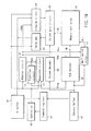
FIG. 16 is a block diagram showing the whole
construction of the memory when this invention is
applied to a flash memory. An address buffer 41
receives an external address and outputs an internal
address corresponding to a memory cell to be subjected
to the readout process, program process or erase
process. An I/O buffer 42 outputs data of a memory
cell to be sensed by a sense amplifier 43 to the
exterior at the readout time and inputs program data
supplied from the exterior to a program circuit 44 at
the program time. The program circuit 44 supplies
program voltage to a corresponding one of bit lines in
a memory cell array 46 via a column gate circuit 45.
-
A command register 47 holds commands such as
program and erase commands supplied from the exterior
and a controller 48 receives the command held in the
command register 47 and outputs control signals for
controlling various circuits in the memory. A row
decoder 49 receives the internal address output from
the address buffer 41 to select a corresponding one of
word lines in the memory cell array 46. A column
decoder 50 receives the internal address output from
the address buffer 41 to selectively drive the column
gate in the column gate circuit 45 according to
the internal address. As a result, the selected bit
line in the memory cell array 46 is connected to the
sense amplifier 43 via the column gate circuit 45.
-
A booster circuit 51 includes a charge pump
circuit and the like, generates positive voltages Vpp,
Vddp higher than the external power supply voltage by
boosting or raising the external power supply voltage
and generates 0V or negative voltage Vbb. The voltage
Vddp generated from the booster circuit 51 is supplied
to the program circuit 44. The voltage Vpp generated
from the booster circuit 51 is supplied to the
regulator circuit 12. The function of the regulator
circuit 12 is the same as described before and the
explanation thereof is omitted. The equalizer circuit
13 described before is connected between the booster
circuit 51 and the regulator circuit 12. Also, the
function of the equalizer circuit 13 is the same as
described before and the explanation thereof is
omitted.
-
The voltage Vpp generated from the booster circuit
51 is also supplied to the well switch circuit 52.
The well switch circuit 52 corresponds to the well
switch circuit 14 shown in FIG. 15, selects the voltage
Vpp output from the booster circuit 51 according to
the internal address output from the address buffer 41
at the erase time and outputs the selected voltage to
the source line SLi in the memory cell array 46 shown
in FIG. 2.
-
The negative voltage Vbb generated from the
booster circuit 51 is supplied to the row decoder 49.
-
In the flash memory with the above construction,
since the voltage Vreg with various values to be
supplied to the word line, that is, the control gate
electrode of the memory cell at the program time or
readout time of the memory cell is obtained by using
voltage generated from one booster circuit (charge pump
circuit) and changing the voltage to voltage having
a plurality of values smaller than that of the above
voltage by use of the regulator circuit 12, it becomes
unnecessary to use a plurality of charge pump circuits.
As a result, the whole area of the chip can be
prevented from becoming large. In addition, since
a relatively large current flows in the charge pump
circuit and the consumption current is large, the whole
consumption current can be reduced by reducing the
number of charge pump circuits. The voltage Vreg is
supplied to the word line WL of the memory cell array
46, that is, the control gate electrode of the memory
cell via the row decoder 49.
-
The following table 2 indicates the relation
between the various operation modes of the flash memory
of FIG. 16 and the voltages Vpp, Vreg, Vddp, Vbb.
| Operation mode | Vpp | Vreg | Vddp | Vbb |
| Readout |
| | 5V |
| | 5V | Vcc | 0V |
| Program |
| | 10V | 7 to 10V (0.5V step up) | 5V | 0V |
| Program Verify | 10V | 6.5V | 5V | 0V |
| Erase | 10V | 2.5V | 5V | -5 to -7.5V (0.5V step up) |
| Erase Verify | 10V | 4V | | 5V | -1V |
| Excessive Erase Verify | 10V | 2.5V | 5V | -1V |
| Weak Program | 10V (0.5V step up) | 2.5 to 5V | 5V | -1V |
-
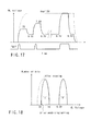
The program operation is performed according to
the step-up program for raising the word line voltage
(control gate voltage of the memory cell) bit by bit.
The relation between the word line (WL) voltage by the
program operation based on the step-up program and the
equalizing control signal EQLE for controlling the
operation of the equalizer circuit 13 is shown in
FIG. 17.
-
In this example, the voltage Vreg generated from
the regulator circuit 12 is stepped up by 0.5V at
one time in a voltage range of 7V to 10V in such
a manner as indicated by 7V, 6.5V, 7.5V, 6.5V, ···, 10V.
In this case, the equalizing control signal EQLE is
activated only at the time of level change at which the
program voltage rises in the range of the program
voltage from 7V to 9.5V. Further, when the program
voltage is set at the same voltage of 10V as the
boosted voltage Vpp, the equalizing control signal EQLE
is activated while the program voltage is kept set at
the voltage of 10V.
-
The program verify mode is a mode in which whether
or not data is sufficiently programmed after
programming is determined by reading out data and, in
the program verify mode, the voltage Vreg or the
voltage supplied to the control gate electrode of
the memory cell is set at 6.5V which is lower than in
the case of program mode. Likewise, the erase verify
mode is a mode in which whether or not data is
sufficiently erased after erasing is determined by
reading out data and, in the erase verify mode, the
voltage Vreg or the voltage supplied to the control
gate electrode of the memory cell is set at 2.5V which
is lower than in the case of erase mode.
-
The threshold voltage of the memory cell
immediately after data erasing is widely distributed as
shown by broken lines in FIG. 18, for example. If the
threshold voltage is excessively lowered, a leak
current flows in the bit line connected to the memory
cell. In this case, if the memory cells other than
the memory cell whose threshold voltage is excessively
lowered are set in the programmed state ("0"), data is
regarded as "1" as viewed from the sense amplifier when
data of the memory cell set in the programmed state is
read out and thus an erroneous operation is effected.
In order to prevent this problem, a weak program
process for slightly re-programming the memory cell set
in the excessively erased state is effected. The weak
program mode is a mode in which the weak program
process is effected. Low word line voltage is supplied
to a memory cell in which data becomes "1" by the
excessive erase verify process to raise the threshold
voltage thereof. The excessive verify process and weak
program process are repeatedly effected until the
satisfactory excessive erase verify process is
effected. At this time, in order to reduce time for
the weak program process, the word line voltage is
raised by 0.5V each time the weak program process is
effected. Then, if the excessive erase verify process
is satisfactorily effected for all of the memory cells
in the block subjected to the erase process, the weak
program operation is terminated.
-
FIG. 19 is a cross sectional view showing the
construction of part of the flash memory of FIG. 16.
N- type well regions 62, 63 are formed in a P-type
semiconductor substrate 61. A P-type well region 64 is
formed in the N-type well region 62. The memory cells
MC in the memory cell array 46 shown in FIG. 16 are
formed in the P-type well region 64. In FIG. 19, only
one of the memory cells MC is shown for brevity of the
drawing.
-
A P-type contact region 65 acting as a contact
region of the well region 64 is formed in the P-type
well region 64 and an N-type contact region 66 acting
as a contact region of the well region 62 is formed in
the N-type well region 62. The contact regions 65, 66
are connected to the source line SL together with the
sources of the memory cells MC and the voltage
generated from the well switch circuit 52 is commonly
supplied to the well regions 62, 64 and the sources of
the memory cells MC via the source line SL. The drain
D of the memory cell MC is connected to a corresponding
one of a plurality of bit lines BL.
-
The memory cell MC has no overlap area between the
floating gate electrode and the source S.
-
In the N-type well region 63, a P-type well region
67 is formed and N-channel and P-channel MOS
transistors of a peripheral circuit which is applied
with high voltage in the flash memory and requires high
breakdown voltage (HV) are formed in the semiconductor
substrate 61, P-type well region 67 and N-type well
region 63.
-
Further, in the P-type semiconductor substrate 61,
a P-type well region 68 and N-type well region 69 are
formed. N-channel and P-channel MOS transistors of
a peripheral circuit of low breakdown voltage (LV)
which does not require high breakdown voltage in the
flash memory are formed in the P-type and N- type well
regions 68, 69.
-
The transistors shown in FIG. 19 are only part of
transistors and a large number of transistors are
actually formed on the semiconductor substrate 61.
-
The readout operation for the flash memory with
the above construction is effected by selecting one
word line WL and applying a voltage of 5V, for example,
to the selected word line WL. At this time, a voltage
of 0V is output from the well switch circuit 52 and the
voltage of 0V is applied to the P-type well region 64
in which the memory cells are formed via the source
line SL. Further, since the sources of the memory
cells MC are connected to the well region 64, the
sources of the memory cells MC are also set at 0V.
-
On the other hand, preset voltage is applied to
the bit line BL of the memory cell. At this time,
since the threshold voltage of the memory cell as
viewed from the word line WL is 5V or less when the
selected cell is a "1" cell, a drain current flows in
the memory cell. In the case of "0" cell, since the
threshold voltage of the memory cell as viewed from the
word line WL is 5V or more, a drain current does not
flow in the memory cell. The current is sensed and
amplified by the sense amplifier and sense data is
output to the exterior.
-
Like the case of the readout operation, in the
program operation, a voltage of 7V to 10V is applied to
the word line WL while it is stepped up by 0.5V at
one time. At this time, a voltage of 0V is output from
the well switch circuit 52.
-
At this time, a voltage of 5V is applied to the
bit line BL according to program data. Therefore, a
current flows in the drain-source path of the selected
cell and hot electrons generated at this time are
injected into the floating gate to raise the threshold
voltage of the cell to 5V or more and thus the program
operation is effected. Since a voltage of 0V is
applied to the program non-selection bit lines BL and
no hot electrons are generated, the threshold voltage
is kept at 5V or less.
-
Next, the erase operation is explained with
reference to the timing chart of FIG. 20. First, an
erase signal ERASE is set to the "H" level at timing
T0. At timing T1 after the timing T0, a voltage of 10V
is output from the well switch circuit 52 so as to
start to charge the well region 64 via the source
line SL. At this time, the rising slope of the voltage
of 10V is made relatively gentle.
-
After the well region 64 is charged to 10V, a
voltage of -6V is output from the row decoder at timing
T2 so as to start to charge the word line WL by the
voltage of -6V.
-
Then, the erasing process is effected when the
well region 64 is set at 10V and the word line WL is
set at -6V. That is, when the word line WL is set
at -6V, the floating gate electrode is set at preset
negative voltage whose absolute value is smaller than
that of -6V by the capacitive coupling between the
control gate electrode and the floating gate electrode.
At this time, a tunnel current flows between the
floating gate electrode and the whole portion of the
channel region of the memory cell to extract electrons
from the floating gate electrode, thereby lowering the
threshold voltage of the memory cell to 5V or less.
Thus, the erase operation is effected.
-
After the erase process is terminated, a voltage
of 0V is output from the row decoder at timing T3 to
reset the word line WL to 0V. It is also required to
slowly effect the reset operation. This is because the
well voltage is excessively raised by the capacitive
coupling between the word line and the well region and
breakdown of the well region or junction breakdown
occurs if the word line WL is abruptly reset to 0V.
-
After this, the well region is rest to 0V at
timing T4. It is also required to slowly effect the
reset operation. This is because the word line
potential is made negative by the capacitive coupling
between word line and the well region and becomes lower
than the well potential (0V) of the N-type MOS
transistor constructing the row decoder to cause the
resultant forward bias state if the reset operation is
effected at excessively high speed.
-
After this, the erase signal ERASE is set at the
"L" level at timing T5 to complete the erase operation.
-
Thus, the data erasing operation is effected by
causing a tunnel current to flow in the whole portion
of the channel region. Further, since an overlap area
between the floating gate electrode and the source is
not formed, the reduction rate of the memory cell size
can be enhanced.
-
As shown in FIG. 19, the P-type well region 64 in
which the memory cells MC are formed and the N-type
well region 62 in which the P-type well region 64 is
formed are both connected to the source line SL. Since
the well region 64 and the source S of the memory cell
are both set at 0V at the program time and readout
time, the well region 64 and the source S can be short-circuited.
Further, at the erase time, the well region
64 and the source S can be biased to the same potential
and they may be short-circuited. Thus, since it is not
necessary to separately form the well interconnection
and the source interconnection, the interconnection
area and the drive circuit for the interconnections can
be reduced.
-
Further, the following table 3 indicates the
relation between the various operation modes of the
memory cell of FIG. 19 and the voltages of the selected
WL, non-selected WL, selected BL (bit line), non-selected
BL, selected source line and non-selected
source line. In this example, voltage is applied to
the selected WL at the erase time in a range of -5V to
-7.5V while it is stepped up by 0.5V at one time.
-
As described above, according to this invention,
a semiconductor device can be provided in which the
number of booster circuits can be reduced to suppress
an increase in the chip area at the time of integration
and the consumption current can be suppressed to a
small value since voltage having variously changing
values is generated from the regulator circuit by using
an output of the booster circuit.