EP1191586A2 - Floating gate memory and manufacturing method - Google Patents
Floating gate memory and manufacturing method Download PDFInfo
- Publication number
- EP1191586A2 EP1191586A2 EP01307993A EP01307993A EP1191586A2 EP 1191586 A2 EP1191586 A2 EP 1191586A2 EP 01307993 A EP01307993 A EP 01307993A EP 01307993 A EP01307993 A EP 01307993A EP 1191586 A2 EP1191586 A2 EP 1191586A2
- Authority
- EP
- European Patent Office
- Prior art keywords
- layer
- trenches
- conductive material
- forming
- blocks
- Prior art date
- Legal status (The legal status is an assumption and is not a legal conclusion. Google has not performed a legal analysis and makes no representation as to the accuracy of the status listed.)
- Withdrawn
Links
- 238000007667 floating Methods 0.000 title claims abstract description 63
- 238000004519 manufacturing process Methods 0.000 title description 3
- 238000000034 method Methods 0.000 claims abstract description 97
- 239000000758 substrate Substances 0.000 claims abstract description 75
- 239000004020 conductor Substances 0.000 claims abstract description 62
- 238000002955 isolation Methods 0.000 claims abstract description 27
- 239000004065 semiconductor Substances 0.000 claims abstract description 23
- 238000007373 indentation Methods 0.000 claims abstract description 10
- 125000006850 spacer group Chemical group 0.000 claims description 51
- XUIMIQQOPSSXEZ-UHFFFAOYSA-N Silicon Chemical compound [Si] XUIMIQQOPSSXEZ-UHFFFAOYSA-N 0.000 claims description 34
- 238000009413 insulation Methods 0.000 claims description 34
- 229910052710 silicon Inorganic materials 0.000 claims description 34
- 239000010703 silicon Substances 0.000 claims description 34
- 239000000463 material Substances 0.000 claims description 30
- 230000015572 biosynthetic process Effects 0.000 claims description 29
- 239000012774 insulation material Substances 0.000 claims description 21
- 238000005530 etching Methods 0.000 claims description 11
- 238000002161 passivation Methods 0.000 claims description 6
- 230000001681 protective effect Effects 0.000 claims description 3
- 230000005689 Fowler Nordheim tunneling Effects 0.000 claims 2
- 239000011810 insulating material Substances 0.000 claims 2
- 239000010410 layer Substances 0.000 description 249
- 150000004767 nitrides Chemical class 0.000 description 70
- 229910052751 metal Inorganic materials 0.000 description 34
- 239000002184 metal Substances 0.000 description 34
- 229910021420 polycrystalline silicon Inorganic materials 0.000 description 26
- 229920005591 polysilicon Polymers 0.000 description 26
- 238000000151 deposition Methods 0.000 description 24
- VYPSYNLAJGMNEJ-UHFFFAOYSA-N Silicium dioxide Chemical compound O=[Si]=O VYPSYNLAJGMNEJ-UHFFFAOYSA-N 0.000 description 18
- 229910021332 silicide Inorganic materials 0.000 description 18
- FVBUAEGBCNSCDD-UHFFFAOYSA-N silicide(4-) Chemical compound [Si-4] FVBUAEGBCNSCDD-UHFFFAOYSA-N 0.000 description 18
- 230000000873 masking effect Effects 0.000 description 17
- 239000005380 borophosphosilicate glass Substances 0.000 description 16
- PXHVJJICTQNCMI-UHFFFAOYSA-N Nickel Chemical compound [Ni] PXHVJJICTQNCMI-UHFFFAOYSA-N 0.000 description 12
- 230000008878 coupling Effects 0.000 description 12
- 238000010168 coupling process Methods 0.000 description 12
- 238000005859 coupling reaction Methods 0.000 description 12
- BASFCYQUMIYNBI-UHFFFAOYSA-N platinum Chemical compound [Pt] BASFCYQUMIYNBI-UHFFFAOYSA-N 0.000 description 12
- 229910052581 Si3N4 Inorganic materials 0.000 description 11
- HQVNEWCFYHHQES-UHFFFAOYSA-N silicon nitride Chemical compound N12[Si]34N5[Si]62N3[Si]51N64 HQVNEWCFYHHQES-UHFFFAOYSA-N 0.000 description 11
- WFKWXMTUELFFGS-UHFFFAOYSA-N tungsten Chemical compound [W] WFKWXMTUELFFGS-UHFFFAOYSA-N 0.000 description 11
- 229910052721 tungsten Inorganic materials 0.000 description 11
- 239000010937 tungsten Substances 0.000 description 11
- 230000008021 deposition Effects 0.000 description 10
- 229960001866 silicon dioxide Drugs 0.000 description 9
- 235000012239 silicon dioxide Nutrition 0.000 description 9
- 239000000377 silicon dioxide Substances 0.000 description 9
- 238000005229 chemical vapour deposition Methods 0.000 description 7
- ZOKXTWBITQBERF-UHFFFAOYSA-N Molybdenum Chemical compound [Mo] ZOKXTWBITQBERF-UHFFFAOYSA-N 0.000 description 6
- RTAQQCXQSZGOHL-UHFFFAOYSA-N Titanium Chemical compound [Ti] RTAQQCXQSZGOHL-UHFFFAOYSA-N 0.000 description 6
- NRTOMJZYCJJWKI-UHFFFAOYSA-N Titanium nitride Chemical compound [Ti]#N NRTOMJZYCJJWKI-UHFFFAOYSA-N 0.000 description 6
- 229910017052 cobalt Inorganic materials 0.000 description 6
- 239000010941 cobalt Substances 0.000 description 6
- GUTLYIVDDKVIGB-UHFFFAOYSA-N cobalt atom Chemical compound [Co] GUTLYIVDDKVIGB-UHFFFAOYSA-N 0.000 description 6
- 238000001465 metallisation Methods 0.000 description 6
- 229910052750 molybdenum Inorganic materials 0.000 description 6
- 239000011733 molybdenum Substances 0.000 description 6
- 229910052759 nickel Inorganic materials 0.000 description 6
- 229910052697 platinum Inorganic materials 0.000 description 6
- 229910052719 titanium Inorganic materials 0.000 description 6
- 239000010936 titanium Substances 0.000 description 6
- 238000005468 ion implantation Methods 0.000 description 5
- 230000003647 oxidation Effects 0.000 description 5
- 238000007254 oxidation reaction Methods 0.000 description 5
- 229920002120 photoresistant polymer Polymers 0.000 description 4
- 239000011241 protective layer Substances 0.000 description 4
- -1 salicide) Chemical compound 0.000 description 4
- 230000001590 oxidative effect Effects 0.000 description 3
- 238000003491 array Methods 0.000 description 2
- 238000005137 deposition process Methods 0.000 description 2
- 238000001514 detection method Methods 0.000 description 2
- 238000005516 engineering process Methods 0.000 description 2
- 239000007943 implant Substances 0.000 description 2
- 238000002347 injection Methods 0.000 description 2
- 239000007924 injection Substances 0.000 description 2
- 239000012212 insulator Substances 0.000 description 2
- 150000002500 ions Chemical class 0.000 description 2
- 238000004518 low pressure chemical vapour deposition Methods 0.000 description 2
- 239000002131 composite material Substances 0.000 description 1
- 230000007423 decrease Effects 0.000 description 1
- 239000003989 dielectric material Substances 0.000 description 1
- 230000000694 effects Effects 0.000 description 1
- 238000002513 implantation Methods 0.000 description 1
- 238000011065 in-situ storage Methods 0.000 description 1
- 230000010354 integration Effects 0.000 description 1
- 238000000059 patterning Methods 0.000 description 1
- 238000000206 photolithography Methods 0.000 description 1
- 238000005498 polishing Methods 0.000 description 1
- 230000005641 tunneling Effects 0.000 description 1
Images


Classifications
-
- H—ELECTRICITY
- H10—SEMICONDUCTOR DEVICES; ELECTRIC SOLID-STATE DEVICES NOT OTHERWISE PROVIDED FOR
- H10B—ELECTRONIC MEMORY DEVICES
- H10B69/00—Erasable-and-programmable ROM [EPROM] devices not provided for in groups H10B41/00 - H10B63/00, e.g. ultraviolet erasable-and-programmable ROM [UVEPROM] devices
-
- H—ELECTRICITY
- H10—SEMICONDUCTOR DEVICES; ELECTRIC SOLID-STATE DEVICES NOT OTHERWISE PROVIDED FOR
- H10B—ELECTRONIC MEMORY DEVICES
- H10B41/00—Electrically erasable-and-programmable ROM [EEPROM] devices comprising floating gates
- H10B41/30—Electrically erasable-and-programmable ROM [EEPROM] devices comprising floating gates characterised by the memory core region
-
- H—ELECTRICITY
- H01—ELECTRIC ELEMENTS
- H01L—SEMICONDUCTOR DEVICES NOT COVERED BY CLASS H10
- H01L29/00—Semiconductor devices adapted for rectifying, amplifying, oscillating or switching, or capacitors or resistors with at least one potential-jump barrier or surface barrier, e.g. PN junction depletion layer or carrier concentration layer; Details of semiconductor bodies or of electrodes thereof ; Multistep manufacturing processes therefor
- H01L29/40—Electrodes ; Multistep manufacturing processes therefor
- H01L29/401—Multistep manufacturing processes
- H01L29/4011—Multistep manufacturing processes for data storage electrodes
- H01L29/40114—Multistep manufacturing processes for data storage electrodes the electrodes comprising a conductor-insulator-conductor-insulator-semiconductor structure
-
- H—ELECTRICITY
- H01—ELECTRIC ELEMENTS
- H01L—SEMICONDUCTOR DEVICES NOT COVERED BY CLASS H10
- H01L29/00—Semiconductor devices adapted for rectifying, amplifying, oscillating or switching, or capacitors or resistors with at least one potential-jump barrier or surface barrier, e.g. PN junction depletion layer or carrier concentration layer; Details of semiconductor bodies or of electrodes thereof ; Multistep manufacturing processes therefor
- H01L29/40—Electrodes ; Multistep manufacturing processes therefor
- H01L29/41—Electrodes ; Multistep manufacturing processes therefor characterised by their shape, relative sizes or dispositions
- H01L29/423—Electrodes ; Multistep manufacturing processes therefor characterised by their shape, relative sizes or dispositions not carrying the current to be rectified, amplified or switched
- H01L29/42312—Gate electrodes for field effect devices
- H01L29/42316—Gate electrodes for field effect devices for field-effect transistors
- H01L29/4232—Gate electrodes for field effect devices for field-effect transistors with insulated gate
- H01L29/42324—Gate electrodes for transistors with a floating gate
-
- H—ELECTRICITY
- H01—ELECTRIC ELEMENTS
- H01L—SEMICONDUCTOR DEVICES NOT COVERED BY CLASS H10
- H01L29/00—Semiconductor devices adapted for rectifying, amplifying, oscillating or switching, or capacitors or resistors with at least one potential-jump barrier or surface barrier, e.g. PN junction depletion layer or carrier concentration layer; Details of semiconductor bodies or of electrodes thereof ; Multistep manufacturing processes therefor
- H01L29/66—Types of semiconductor device ; Multistep manufacturing processes therefor
- H01L29/66007—Multistep manufacturing processes
- H01L29/66075—Multistep manufacturing processes of devices having semiconductor bodies comprising group 14 or group 13/15 materials
- H01L29/66227—Multistep manufacturing processes of devices having semiconductor bodies comprising group 14 or group 13/15 materials the devices being controllable only by the electric current supplied or the electric potential applied, to an electrode which does not carry the current to be rectified, amplified or switched, e.g. three-terminal devices
- H01L29/66409—Unipolar field-effect transistors
- H01L29/66477—Unipolar field-effect transistors with an insulated gate, i.e. MISFET
- H01L29/66825—Unipolar field-effect transistors with an insulated gate, i.e. MISFET with a floating gate
-
- H—ELECTRICITY
- H10—SEMICONDUCTOR DEVICES; ELECTRIC SOLID-STATE DEVICES NOT OTHERWISE PROVIDED FOR
- H10B—ELECTRONIC MEMORY DEVICES
- H10B99/00—Subject matter not provided for in other groups of this subclass
Definitions
- the present invention relates to a self-aligned method of forming a semiconductor memory array of floating gate memory cells of the split gate type.
- the present invention also relates to a semiconductor memory array of floating gate memory cells of the foregoing type.
- Non-volatile semiconductor memory cells using a floating gate to store charges thereon and memory arrays of such non-volatile memory cells formed in a semiconductor substrate are well known in the art.
- floating gate memory cells have been of the split gate type, or stacked gate type, or a combination thereof.
- Self-alignment is well known in the art. Self-alignment refers to the act of processing one or more steps involving one or more materials such that the features are automatically aligned with respect to one another in that step processing. Accordingly, the present invention uses the technique of self-alignment to achieve the manufacturing of a semiconductor memory array of the floating gate memory cell type.
- the present invention solves the above mentioned problems by providing a (T-shaped) source region, where a wider conductive upper portion reduces source line resistance, while a narrower lower portion in the source line facilitates smaller memory cell geometries.
- the memory cell architecture also facilitates the coupling of source voltage to the floating gate through an oxide on the upper portion of the floating gate, in addition to coupling through the bottom coupling oxide, which enhances the coupling coefficient between the source electrode and the floating gate.
- the present invention is a self-aligned method of forming a semiconductor memory array of floating gate memory cells in a semiconductor substrate, each memory cell having a floating gate, a first terminal, a second terminal with a channel region therebetween, and a control gate.
- Tthe method includes the steps of:
- an electrically programmable and erasable memory device in another aspect of the present invention, includes a substrate of semiconductor material of a first conductivity type, first and second spaced-apart regions in the substrate of a second conductivity type with a channel region therebetween, a first insulation layer disposed over said substrate, an electrically conductive floating gate disposed over said first insulation layer and extending over a portion of the channel region and over a portion of the first region, and an electrically conductive source region disposed over and electrically connected to the first region in the substrate.
- the source region has a lower portion that is disposed adjacent to and insulated from the floating gate and an upper portion that is disposed over and insulated from the floating gate.
- an array of electrically programmable and erasable memory devices includes: a substrate of semiconductor material of a first conductivity type, spaced apart isolation regions formed on the substrate which are substantially parallel to one another and extend in a first direction with an active region between each pair of adjacent isolation regions, and each of the active regions includes a column of pairs of memory cells extending in the first direction.
- Each of the memory cell pairs includes a first region and a pair of second regions spaced apart in the substrate having a second conductivity type with channel regions formed in the substrate between the first region and the second regions, a first insulation layer disposed over said substrate including over the channel regions, a pair of electrically conductive floating gates each disposed over the first insulation layer and extending over a portion of one of the channel regions and over a portion of the first region, and an electrically conductive source region disposed over and electrically connected to the first region in the substrate.
- the source region has a lower portion that is disposed adjacent to and insulated from the pair of floating gates and an upper portion that is disposed over and insulated from the pair of floating gates.
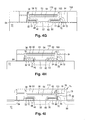
- FIG. 1A is a top view of a semiconductor substrate used in the first step of the method of present invention to form isolation regions.
- FIG. 1B is a cross sectional view taken along the line 1-1.
- FIG. 1C is a top view of the next step in the processing of the structure of Fig. 1B, in which isolation regions are formed.
- FIG. 1D is a cross sectional view of the structure in Fig. 1C taken along the line 1-1 showing the isolation stripes formed in the structure.
- FIG. 1E is a cross sectional view of the structure in Fig. 1C taken along the line 1-1 showing the two types of isolation regions that can be formed in the semiconductor substrate: LOCOS or shallow trench.
- FIGs. 2A-2N are cross sectional views taken along the line 2-2 of Fig. 1C showing in sequence the next step(s) in the processing of the structure shown in Fig. 1C, in the formation of a non volatile memory array of floating memory cells of the split gate type.
- FIG. 20 is a top view showing the interconnection of row lines and bit lines to terminals in active regions in the formation of the non volatile memory array of floating memory cells of the split gate type.
- FIGs. 3A-3I are cross sectional views taken along the line 2-2 of Fig. 1C showing in sequence the steps in a first alternate processing of the structure shown in Fig. 1C, in the formation of a non volatile memory array of floating memory cells of the split gate type.
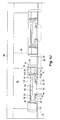
- FIGs. 4A-4J are cross sectional views taken along the line 2-2 of Fig. 1C showing in sequence the steps in a second alternate processing of the structure shown in Fig. 1C, in the formation of a non volatile memory array of floating memory cells of the split gate type.
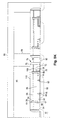
- FIGs. 5A-5K are cross sectional views taken along the line 2-2 of Fig. 1C showing in sequence the steps in a third alternate processing of the structure shown in Fig. 1C, in the formation of a non volatile memory array of floating memory cells of the split gate type.
- a first layer of insulation material 12 such as silicon dioxide (oxide) is deposited thereon as shown in Fig. 1B.
- the first insulation layer 12 is formed on the substrate 10 by well known techniques such as oxidation or deposition (e.g. chemical vapor deposition or CVD), forming a layer of silicon dioxide (hereinafter "oxide").
- a first layer of polysilicon 14 (FG poly) is deposited on top of the first layer of insulation material 12.
- the deposition and formation of the first polysilicon layer 14 on the first insulation layer 12 can be made by a well known process such as Low Pressure CVD or LPCVD.
- a silicon nitride layer 18 (hereinafter “nitride”) is deposited over the polysilicon layer 14, preferably by CVD. This nitride layer 18 is used to define the active regions during isolation formation.
- nitride silicon nitride layer 18
- all of the forgoing described parameters and the parameters described hereinafter, depend upon the design rules and the process technology generation. What is described herein is for the 0.18 micron process. However, it will be understood by those skilled in the art that the present invention is not limited to any specific process technology generation, nor to any specific value in any of the process parameters described hereinafter.
- suitable photo-resistant material 19 is applied on the silicon nitride layer 18 and a masking step is performed to selectively remove the photo-resistant material from certain regions (stripes 16).
- the photo-resist material 19 is removed, the silicon nitride 18, the polysilicon 14 and the underlying insulation material 12 are etched away in stripes 16 formed in the Y direction or the column direction, as shown in Fig. 1C, using standard etching techniques (i.e. anisotropic etch process).
- the distance W between adjacent stripes 16 can be as small as the smallest lithographic feature of the process used.
- the silicon nitride 18, the first polysilicon region 14 and the underlying insulation region 12 are maintained.
- the resulting structure is illustrated in Fig. 1D.
- LOCOS low-oxide-semiconductor
- STI shallow-semiconductor
- the structure is further processed to remove the remaining photo resist 19.
- an isolation material 20a or 20b such as silicon dioxide, is formed in the regions or "grooves" 16.
- the nitride layer 18 is then selectively removed to form the structure shown in Fig. 1E.
- the isolation can be formed via the well known LOCOS process resulting in the local field oxide 20a (e.g. by oxidizing the exposed substrate), or it can be formed via a shallow trench process (STI) resulting in silicon-dioxide being formed in the region 20b (e.g. by depositing an oxide layer, followed by a Chemical-Mechanical-Polishing or CMP etch). It should be noted that during the LOCOS formation, a spacer may be necessary to protect the side walls of poly layer 14 during the formation of the local field oxide.
- STI shallow trench process
- the remaining first polysilicon layer 14 and the underlying first insulation material 12 form the active regions.
- the substrate 10 has alternating stripes of active regions and isolation regions with the isolation regions being formed of either LOCOS insulation material 20a or shallow trench insulation material 20b.
- Fig. 1E shows the formation of both a LOCOS region 20a and a shallow trench region 20b, only one of the LOCOS process (20a) or the shallow trench process (20b) will be used. In the preferred embodiment, the shallow trench 20b will be formed. Shallow trench 20b is preferable because it can be more precisely formed at smaller design rules.
- the structure in Fig. 1E represents a self aligned structure, which is more compact than a structure formed by a non self-aligned method.
- a non self-aligned method of forming the structure shown in Figure 1E is as follows. Regions of isolation 20 are first formed in the substrate 10. This can be done by depositing a layer of silicon nitride on the substrate 10, depositing photo-resist, patterning the silicon nitride using a first masking step to expose selective portions of the substrate 10, and then oxidizing the exposed substrate 10 using either the LOCOS process or the STI process where silicon trench formation and trench fill are involved.
- the silicon nitride is removed, and a first layer of silicon dioxide 12 (to form the gate oxide) is deposited over the substrate 10.
- a first layer of polysilicon 14 is deposited over the gate oxide 12.
- the first layer of polysilicon 14 is then patterned using a second masking step and selective portions removed.
- the polysilicon 14 is not self aligned with the regions of isolation 20, and a second masking step is required. Further, the additional masking step requires that the dimensions of the polysilicon 14 have an alignment tolerance with respect to the regions of isolation 20. It should be noted that the non self-aligned method does not utilize nitride layer 18.
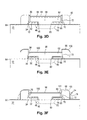
- Fig. 2A which shows the structure from a view orthogonal to that of Figs. 1B and 1E, the next steps in the process of the present invention are illustrated.
- a thick insulation layer 24, such as silicon nitride (hereinafter "nitride”) is formed on the structure, followed by the formation of a thin protective layer 26 such as polysilicon (hereinafter "poly").
- poly polysilicon
- a conventional photo-lithography masking operation is performed with photo-resist applied on top of the poly layer 26.
- a masking step is applied in which stripes (i.e. masking regions) are defined in the X or the row direction. The distance between adjacent stripes can be a size determined by the needs of the device to be fabricated.
- the photo resist is removed in defined masking regions, i.e. stripes in the row direction, after which poly layer 26 underlying the removed photo resist is etched away in the stripes using a conventional anisotropic poly etch process to expose portions of the underlying nitride layer 24.
- An anisotropic nitride etch process is then performed to remove the exposed portions of nitride layer 24 to expose portions of poly layer 14.
- An optional poly etch process can follow to remove just a top portion of the exposed poly layer 14, to slightly recess poly layer 14 relative to the remaining nitride layer 24, and to form sloped portions 28 of poly layer 14 where it meets nitride layer 24.
- these etch processes result in the formation of a single first trench 30 that extends down to (and preferably slightly into) polysilicon layer 14. The remaining photo-resist is then removed, resulting in the structure shown in Fig. 2B.
- a layer 32 of insulation material, such as silicon dioxide (hereinafter “oxide”) is then formed over the structure using, for example, a thermal oxidation process.
- oxide silicon dioxide
- the portions of oxide layer 32 formed on poly layer 14 in trenches 30 have raised portions 34 caused by sloped portions 28 of poly layer 14, giving oxide layer 32 inside trenches 30 a lens shape.
- Fig. 2C The resulting structure is illustrated in Fig. 2C.
- Insulation spacers 40 are then formed inside trenches 30 (Fig. 2E). Formation of spacers is well known in the art by depositing a material over the contour of a structure, followed by an anisotropic etch process (e.g. RIE), whereby the material is removed from horizontal surfaces of the structure, while the material remains largely intact on vertically oriented surfaces of the structure. Spacers 40 can be formed of any dielectric material. In the preferred embodiment, spacers 40 are formed of nitride in the following manner. A thin layer 36 of insulation material (i.e. oxide) is formed over the structure of Fig. 2C preferably using a conventional chemical vapor deposition (CVD) process. A thick layer 38 of insulation material (i.e.
- CVD chemical vapor deposition
- nitride is then formed over the structure preferably by a conventional nitride deposition process, as shown in Fig. 2D.
- a thick nitride etch process that uses oxide layer 36 as an etch stop.
- This etch process removes all of nitride layer 38, except for sidewall spacers 40 along the sidewalls of trenches 30.
- An anisotropic oxide etch process is then performed that uses poly layer 26 as an etch stop.
- This oxide etch removes exposed portions of oxide layers 36 and 32 that are over nitride layer 24.
- the oxide etch also removes portion of oxide layers 36 and 32 that are exposed in trenches 30 between spacers 40, to expose portions of poly layer 14 at the centers of the trenches 30.
- the resulting structure is shown in Fig. 2E.
- a thick nitride etch process is performed to remove spacers 40 from trenches 30.
- a poly etch process is then performed to remove poly layer 26 to expose nitride layer 24, and to remove the exposed portions of poly layer 14 at the bottom center of trenches 30 to expose oxide layer 12.
- trenches 30 each have a narrow lower portion 42 bounded by poly layer 14 and oxide layers 32 and 36, and an upper wider portion 44 bounded by oxide layer 36. It should be noted that the spacers 40 can be removed after the poly etch process that removes portions of poly layer 14.
- Insulation spacers 46 are formed on sidewalls of the lower portions 42 of trenches 30.
- oxide spacer 46 formation is preceded by first forming an insulation sidewall layer 48 (oxide) on the sides of polysilicon layer 14 that are exposed inside trenches 30 (i.e. by oxidizing the structure or by CVD). Then, oxide is formed over the structure (i.e.
- oxide anisotropic etch which removes the oxide formed over the structure, except for oxide spacers 46 formed on the sidewalls of lower trench portion 42.
- This oxide formation and etch process also adds to the thickness of the vertical portion of oxide layer 36 in upper trench portion 44.
- the anisotropic etch also removes a top portion of oxide layer 36, thins down the portion of oxide layer 36 over oxide layer 32, as well as removes the portion of oxide layer 12 at the bottom of trenches 30 in between spacers 46 to expose the substrate 10.
- the resulting structure is shown in Fig. 2G.
- a conductive layer 52 such as titanium nitride which adheres well to the exposed substrate 10, is formed over the entire structure, which lines the sidewalls of trenches 30 and exposed substrate 10 therein.
- a tungsten etch-back step follows to remove any tungsten outside of trenches 30, and to preferably define the top surfaces of conductive blocks 54 below the tops of oxide layers 36.
- a conductive layer 56 (titanium nitride) is then formed over conductive blocks 54, preferably by depositing titanium nitride over the structure, followed by a planarizing (CMP) process that removes the deposited titanium nitride except for the conductive layer 56 over conductive blocks 54 in trenches 30.
- CMP planarizing
- a titanium nitride etch is then performed so that conductive layer 56 is recessed below the top of oxide layer 36.
- a layer 58 of insulation material (oxide) is then formed over the structure, followed by a planarization process (CMP) and oxide etch process to remove the deposited oxide except for that portion over conductive layer 56.
- CMP planarization process
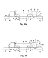
- Second trenches 63 are formed between pair sets of memory cells and adjacent to first trenches 30 in the following manner.
- Nitride layer 24 is removed, preferably using an isotropic etch process, to expose portions of poly layer 14 and oxide layer 32 as shown in Fig. 2I.
- a poly etch process follows (i.e. a dry etch) to remove exposed portions of poly layer 14 and to expose oxide layer 12.
- the exposed portions of oxide layer 12 are then removed via a controlled oxide etch, exposing substrate 10.
- An insulation layer 64 preferably oxide, is then formed over the entire structure, resulting in the structure shown in Fig. 2J.
- the raised portions 34 of oxide layer 32 result in the formation of upwardly extending sharp edges 66 of poly layer 14 where layer 14 meets oxide layer 64.
- Control gate poly blocks are formed in second trenches 63 in the following manner.
- a thick layer of polysilicon is deposited over the structure, followed by an anisotropic poly etch process, which removes all the deposited polysilicon except for poly spacers (blocks) 68 formed against vertically oriented portions of oxide layer 64.
- Poly blocks 68 have lower portions 70 disposed immediately adjacent to poly layer 14, and upper portions 72 that extend over a portion of the poly layer 14 including sharp edge 66.
- Poly blocks 68 are insulated from poly layer 14 by oxide layers 64 and 32. The resulting structure is illustrated in Fig. 2K.
- Insulation spacers 74 are then formed adjacent to poly blocks 68, and are made of one or more layers of material.
- insulation spacers 74 are made of two layers of material by first depositing a thin layer 76 of oxide, followed by the deposition of nitride over the structure. An anisotropic nitride etch is performed to remove the deposited nitride, leaving nitride spacers 78. Ion implantation (e.g. N+) is then used to form second regions (terminals) 80 in the substrate in the same manner as the first regions 50 were formed. A controlled oxide etch follows, which removes the exposed portions of oxide layer 76, as well as the exposed portions of oxide layer 64 to expose substrate 10 and the second regions 80. The resulting structure is shown in Fig. 2L.
- a layer of metalized silicon (silicide) 82 is formed in the top of the substrate 10 next to side wall spacers 74, along with a layer of metalized silicon 84 over poly blocks 68, by depositing a metal such as tungsten, cobalt, titanium, nickel, platinum, or molybdenum over the structure.
- the structure is then annealed, permitting the hot metal to flow and to seep into the exposed top portions of the substrate to form silicide 82, and into the exposed top portions of poly blocks 68 to form metalized silicon 84.
- the metal deposited on the remaining structure is removed by a metal etch process.
- Metalized silicon region 82 on substrate 10 can be called self aligned silicide (i.e. salicide), because it is self aligned to the second regions 80 by spacers 78.
- the resulting structure is shown in Fig. 2M.
- Passivation such as BPSG 86
- a masking step is performed to define etching areas over the silicide regions 82.
- the BPSG 86 is selectively etched in the masked regions to create contact openings that are ideally centered over and extend down to silicide regions 82 formed between adjacent sets of paired memory cells.
- the contact openings are then filled with a conductor metal by metal deposition and planarization etch-back to form contact conductors 88.
- the silicide layers 82 facilitate conduction between the conductors 88 and second regions 80.
- a bit line 90 is added by metal masking over the BPSG 86, to connect together all the conductors 88 in the column of memory cells.
- the final memory cell structure is illustrated in Fig. 2N.
- first and second regions 50/80 form the source and drain for each cell (those skilled in the art know that source and drain can be switched during operation).
- the channel region 92 for each cell is the portion of the substrate that is in-between the source and drain 50/80.
- Poly blocks 68 constitute the control gate, and poly layer 14 constitutes the floating gate.
- Oxide layers 32, 36, 46 and 48 together form an insulation layer that is disposed adjacent to and over floating gate 14, to isolate it from source 96.
- Oxide layers 36 and 64 together form an insulation layer that isolates the source lines 96 from the control gates 68.
- the control gates 68 have one side aligned to the edge of the second region 80, and are disposed over part of the channel regions 92.
- Control gates 68 have lower portions 70 that are disposed adjacent to the floating gates 14 (insulated therefrom by oxide layer 64), and upper protruding portions 72 that are disposed (extend) over a portion of adjacent poly layers 14 (insulated therefrom by oxide layers 64).
- a notch 94 is formed by the protruding portion 72, where the sharp edge 66 of floating gate 14 extends into the notch 94.
- Each floating gate 14 is disposed over part of the channel region 92, is partially overlapped at one end by the control gate 68, and partially overlaps the first region 50 with its other end.
- Conductive blocks 54 and the conductive layers 52/56 together form source lines 96 that extend across the columns of memory cells.
- Upper portions 62 of source lines 96 extend over but are insulated from the floating gates 14, while lower portions 60 of source lines 96 are adjacent to but insulated from floating gates 14.
- the process of the present invention forms pairs of memory cells that mirror each other.
- the pairs of mirrored memory cells are insulated from other cell pairs by oxide layer 76, nitride spacers 78 and BPSG 86.
- FIG. 20 there is shown a top plan view of the resulting structure and the interconnection of the bit lines 90 to the second regions 80, of the control lines 68 which run in the X or the row direction, and of the source lines 96 which connect to the first regions 50 within the substrate 10.
- the source lines 96 make contact with the substrate 10 in the entire row direction, i.e. contact with the active regions as well as the isolation regions, the source lines 96 electrically connect only to the first regions 50 in the substrate 10.
- each first region 50 to which the "source” line 96 is connected is shared between two adjacent memory cells.
- each second region 80 to which the bit line 90 is connected is shared between adjacent memory cells from different mirror sets of memory cells.
- the result is a plurality of non volatile memory cells of the split gate type having a floating gate 14, a control gate 68 which is immediately adjacent to but separated from the floating gate 14 and runs along the length of the row direction connecting to the control gates of other memory cells in the same row, a source line 96 which also runs along the row direction, connecting pairs of the first regions 50 of the memory cells in the same row direction, and a bit line 90 which runs along the column or Y direction and connects pairs of the second regions 80 of the memory cells in the same column direction.
- the formation of the control gate, the floating gate, the source line, and the bit line, are all self-aligned.
- the non-volatile memory cell is of the split gate type having floating gate to control gate tunneling all as described in U.S. Patent No. 5,572,054, whose disclosure is incorporated herein by reference with regard to the operation of such a non-volatile memory cell and an array formed thereby.
- the present invention exhibits reduced source line resistance because of the wider upper portion 62 of T-shaped conductive block 52, while still providing for smaller scaling of memory cell dimensions due to the narrower lower portions 60 of T-shaped conductive blocks 52 (i.e. the indentation of the sidewalls of the first trenches 30 between upper and lower portions 62/60 that forms the T-shape of the source line).
- the upper portions 62 also extend over but are insulated from the floating gates 14 which allows coupling of source voltage from the source line 96 to the floating gates 14 through the oxide layers 32/36 (which is in addition to the coupling via the lower portions 60 through oxide layers 46/48, and via first region 50 through oxide layer 12).
- the coupling coefficient between the source electrode and the floating gate is enhanced.
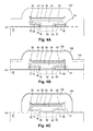
- Figures 3A-3I illustrate a first alternate process for forming a memory cell array similar to that illustrated in Fig. 2N, but with a polysilicon source line. This first alternate process begins with the same structure as shown in Fig. 2G, but continues as follows.
- Conductive blocks 98 are formed inside trenches 30, preferably by depositing a conductive material such as polysilicon over the structure, followed by a poly planarization process (preferably CMP) to remove polysilicon above trenches 30.
- a poly etch-back step follows to remove any polysilicon outside of trenches 30, and to recess the top surfaces of conductive blocks 98 below the tops of oxide layers 36.
- the poly blocks 98 can be in-Situ doped or doped using implantation.
- a layer 58 of insulation material (oxide) is then formed over poly blocks 98, for example by thermal oxidation, or by oxide deposition followed by a CMP planarization process and an oxide etch process so that oxide layer 58 is recessed below the top of oxide layer 36.
- the resulting structure is shown in Fig. 3A, where the narrow/wide trench portions 42/44 result in substantially T-shaped conductive poly blocks 98 with narrow lower block portions 60 and wider upper block portions 62.
- Second trenches 63 are formed between pair sets of memory cells and adjacent to first trenches 30 in the following manner.
- Nitride layer 24 is removed, preferably using an isotropic etch process, to expose portions of poly layer 14 and oxide layer 32 as shown in Fig. 3B.
- a poly etch process follows (i.e. a dry etch) to remove exposed portions of poly layer 14 and to expose portions of oxide layer 12.
- the exposed portions of oxide layer 12 are then removed via a controlled oxide etch, exposing substrate 10.
- An insulation layer 64 preferably oxide, is then formed over the entire structure, resulting in the structure shown in Fig. 3C.
- the raised portions 34 of oxide layer 32 result in the formation of upwardly extending sharp edges 66 of poly layer 14 where layer 14 meets oxide layer 64.
- Control gate poly blocks are formed in second trenches 63 in the following manner.
- a thick layer of polysilicon is deposited over the structure, followed by an anisotropic poly etch process, which removes all the deposited polysilicon except for poly spacers (blocks) 68 formed against vertically oriented portions of oxide layer 64.
- Poly blocks 68 have lower portions 70 disposed immediately adjacent to poly layer 14, and upper portions 72 that extend over a portion of the poly layers 14 including sharp edges 66.
- Poly blocks 68 are insulated from poly layer 14 by oxide layers 64 and 32. 'The resulting structure is illustrated in Fig. 3D.
- An oxide etch is performed to remove exposed portions of oxide layer 64, and the underlying oxide layer 58, to expose poly blocks 98 and substrate 10.
- a dry-etch process with end-point detection is used, which also removes the upper portions of oxide layer 36, so that it is substantially even with the top surface of poly blocks 98.
- An oxide deposition process follows to form an oxide layer 100 over the structure, and to replace oxide layer 64 over the substrate 10. The resulting structure is illustrated in Fig. 3E.
- Insulation spacers 74 are then formed adjacent to poly blocks 68, and are made of one or more layers of material.
- insulation spacers 74 are composite spacers that include lower portions of oxide layer 100 and nitride spacers 78 formed by the deposition of nitride over the structure followed by an anisotropic nitride etch to remove the deposited nitride (using the oxide layer 100 as an etch stop), leaving nitride spacers 78 over oxide layer 64 and adjacent to poly spacers 68.
- Nitride spacers 101 are also formed over the ends of conductive blocks 98, as shown in Fig. 3F.
- Ion implantation e.g. N+
- Ion implantation e.g. N+
- a controlled oxide etch follows to remove the exposed portions of oxide layer 100 to expose poly blocks 98, and to remove exposed portions of oxide layer 64 to expose the substrate 10. The resulting structure is shown in Fig. 3G.
- a layer of metalized silicon (silicide) 82 is formed in the top of the substrate 10 next to side wall spacers 74, along with a layer of metalized silicon 84 over poly blocks 68 and poly block 98, by depositing a metal such as tungsten, cobalt, titanium, nickel, platinum, or molybdenum over the structure.
- the structure is then annealed, permitting the hot metal to flow and to seep into the exposed top portions of the substrate to form silicide 82, and into the exposed top portions of poly blocks 68 and 98 to form metalized silicon 84.
- the metal deposited on the remaining structure is removed by a metal etch process.
- Metalized silicon region 82 on substrate 10 can be called self aligned silicide (i.e. salicide), because it is self aligned to the second regions 80 by spacers 78.
- the resulting structure is shown in Fig. 3H.
- Passivation such as BPSG 86
- a masking step is performed to define etching areas over the silicide regions 82.
- the BPSG 86 is selectively etched in the masked regions to create contact openings that are ideally centered over and extend down to silicide regions 82 formed between adjacent sets of paired memory cells.
- the contact openings are then filled with a conductor metal by metal deposition and planarization etch-back to form contact conductors 88.
- the silicide layers 82 facilitate conduction between the conductors 88 and second regions 80.
- a bit line 90 is added by metal masking over the BPSG 86, to connect together all the conductors 88 in the column of memory cells.
- the final memory cell structure is illustrated in Fig. 3I.
- the first alternate embodiment exhibits reduced source line resistance because of the wider upper portion 62 of T-shaped poly block 98 and the highly conductive metalized silicon layer 84 formed thereon, while still providing for smaller scaling of memory cell dimensions due to the narrower lower portion 60 of T-shaped conductive block 98.
- the upper portions 62 also extend over the floating gate 14 which allows coupling of source voltage from the poly block 98 to the floating gate 14 through the oxide layers 32/36 (in addition to the coupling through the oxide layers 46/48 via lower portions 60, and through the oxide layer 12 via first region 50).
- the coupling coefficient between the source electrode and the floating gate is enhanced.
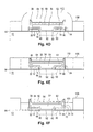
- Figures 4A-4I illustrate a second alternate process for forming a memory cell array similar to that illustrated in Fig. 2N, but utilizing a self aligned contact scheme. This second alternate process begins with the same structure as shown in Fig. 2J, but continues as follows.
- a layer of nitride 104 is then deposited over the structure, followed by a nitride planarization process (e.g. CMP).
- a nitride etch-back step follows to remove the portions of nitride layer 104 over the raised portions of poly layer 102, while leaving portions of nitride layer 104 over the flat side portions of poly layer 102.
- An oxidation step follows, which oxidizes the exposed center portions of poly layer 102 to form a layer of oxide 106 thereover.
- the resulting structure is shown in Fig. 4B.
- Nitride layer 104 is removed by a nitride etch process, which is followed by an anisotropic poly etch step to remove those portions of poly layer 102 not directly under oxide layer 106, as illustrated in Fig. 4C.
- An oxide deposition step is then performed to apply a thick oxide layer over the structure. This is followed by a planarizing oxide etch, such as CMP, to planarize the structure using poly layer 102 as an etch stop.
- a planarizing oxide etch such as CMP
- An oxide etch-back step is then performed, leaving blocks 108 of oxide on either side of the poly layer 102.
- Oxide layer 106 is also removed by the oxide planarizing and etch-back steps, resulting in the structure shown in Fig. 4D.
- a planarizing poly etch, such as CMP is then performed using the oxide blocks 108 as an etch stop, as illustrated in Fig. 4E.
- Poly blocks 103 have lower portions 70 disposed immediately adjacent to poly layer 14, and upper portions 72 that extend over a portion of the poly layer 14 including sharp edge 66.
- Poly blocks 103 are insulated from poly layer 14 by oxide layers 64 and 32. Oxide blocks 108 and oxide layer 36 are left to extend well above the top surface of poly blocks 103, as illustrated in Fig. 4F.
- An optional implant step can be performed to dope the exposed poly blocks 103.
- a metal deposition step is then performed, to deposit a metal such as tungsten, cobalt, titanium, nickel, platinum, or molybdenum over the structure.
- the structure is then annealed, permitting the hot metal to flow and to seep into the exposed top portions of the poly blocks 103 to form a conductive layer of metalized silicon 84 thereon.
- the metal deposited on the remaining structure is removed by a metal etch process.
- Metalized silicon layer 84 can be called self aligned because it is self aligned to the poly blocks 103 by oxide layer 64 and oxide blocks 108.
- a protective nitride layer 110 is formed over poly blocks 103 and between oxide blocks 108 in the following manner.
- Nitride is deposited over the structure, followed by a planarizing nitride etch, such as CMP, with oxide blocks 108 used as the etching stop layer, so that nitride layer 110 is level with oxide blocks 108.
- the nitride layer 110 is self aligned to the poly blocks 103 by oxide blocks 108.
- the resulting structure is shown in Fig. 4G.
- Insulation spacers 74 are then formed adjacent to poly blocks 103 and nitride layer 110, and are made of one or more layers of material. In the preferred embodiment, insulation spacers 74 are made of two layers of material by first depositing a thin layer 76 of oxide, followed by the deposition of a nitride over the structure. An anisotropic nitride etch is performed to remove the deposited nitride, leaving nitride spacers 78. Ion implantation (e.g. N+) is then used to form second regions (terminals) 80 in the substrate in the same manner as the first regions 50 were formed.
- Ion implantation e.g. N+
- a layer of metalized silicon (silicide) 82 is formed in the top of the substrate 10 next to side wall spacers 74, by depositing a metal such as tungsten, cobalt, titanium, nickel, platinum, or molybdenum over the structure. The structure is then annealed, permitting the hot metal to flow and to seep into the exposed top portions of the substrate 10 to form silicide regions 82. The metal deposited on the remaining structure is removed by a metal etch process. Metalized silicon region 82 on substrate 10 can be called self aligned silicide (i.e. salicide), because it is self aligned to the second regions 80 by spacers 78. The resulting structure is shown in Fig. 4I.
- Passivation such as BPSG 86, is used to cover the entire structure.
- a masking step is performed to define etching areas over the salicide regions 82.
- the BPSG 86 is selectively etched in the masked regions to create contact openings that are ideally centered over and wider than the salicide regions 82 formed between adjacent sets of paired memory cells.
- Nitride layer 110 serves to protect poly blocks 103 and metalized silicon 84 from this etch process.
- the contact openings are then filled with a conductor metal by metal deposition and planarizing etch-back, whereby the entire area between nitride spacers 78 of adjacent sets of paired memory cells is filled with the deposited metal to form contact conductors 88 that are self aligned to the salicide regions 82 by the nitride spacers 78 (i.e. self aligned contact scheme, or SAC).
- the salicide layers 82 facilitate conduction between the conductors 88 and second regions 80.
- a bit line 90 is added by metal masking over the BPSG 86, to connect together all the conductors 88 in the column of memory cells.
- the final memory cell structure is illustrated in Fig. 4J.
- the self aligned contact scheme removes an important constraint on the minimum spacing requirement between adjacent sets of paired memory cells.
- Fig. 4J illustrates the contact area (and thus conductors 88) perfectly centered over the salicide regions 82, in reality it is very difficult to form the contact openings without some undesirable horizontal shift relative to the salicide regions 82.
- electrical shorts can occur if the contact 88 is shifted over and formed over metalized silicon 84 and poly block 103.
- the contact openings would have to be formed sufficiently away from the nitride spacers 78 so that even with the maximum possible shift in the contact regions, they will not extend to nitride spacers 78 or beyond. This of course would present a constraint on the minimum distance between spacers 78, in order to provide a sufficient tolerance distance between adjacent sets of paired mirror cells.
- the SAC method of the present invention eliminates this constraint by using the protective layer of material (nitride layer 110) underneath the BPSG.
- the contact openings are formed in the BPSG with a sufficient width to ensure there is overlap of the contact opening with the salicide regions 82, even if there is a significant horizontal shift of the contact opening during formation.
- Nitride layer 110 allows portions of contact 88 to be formed over poly block 103 or metalized silicon layer 84, without any shorting therebetween.
- the wide contact opening guarantees that contacts 88 completely fill the very narrow spaces between spacers 78, and make good electrical contact with salicide regions 82.
- the width of contact regions between spacers 78 can be minimized, while preventing faulty connections by filling the space between spacers 78, allowing the scaling down of the overall cell dimension.
- control gates 103 are substantially rectangularly shaped with a protruding portion 72 over the floating gate 14, and a planar opposing surface that facilitates the formation of spacers 74, which in turn facilitates the self aligned formation of the salicide regions 82, and the formation of the self aligned conductor 88.
- FIGS 5A-5K illustrate a third alternate process for forming a memory cell array similar to that illustrated in Fig. 3I, but utilizing a self aligned contact scheme.
- This third alternate process begins with the same structure as shown in Fig. 3C, but continues as follows.
- a layer of nitride 104 is then deposited over the structure, followed by a nitride planarization process (e.g. CMP).
- a nitride etch-back step follows to remove the portions of nitride layer 104 over the raised portions of poly layer 102, while leaving portions of nitride layer 104 over the flat side portions of poly layer 102.
- An oxidation step follows, which oxidizes the exposed center portions of poly layer 102 to form a layer of oxide 106 thereover. The resulting structure is shown in Fig. 5B.
- Nitride layer 104 is removed by a nitride etch process, which is followed by an anisotropic poly etch step to remove those portions of poly layer 102 not directly under oxide layer 106, as illustrated in Fig. 5C.
- An oxide deposition step is then performed to apply a thick oxide layer 108 over the structure. This is followed by a planarizing oxide etch, such as CMP, to planarize the structure using poly layer 102 as an etch stop. An oxide etch-back step is then performed, leaving blocks 108 of oxide on either side of the poly layer 102. Oxide layer 106 is also removed by the oxide planarizing and etch-back steps.
- a nitride deposition step is then performed to apply a nitride layer over the structure. This is followed by a planarizing nitride etch, such as CMP, to planarize the structure using poly layer 102 as an etch stop. A nitride etch-back step is then performed, leaving nitride layer 109 over oxide blocks 108. The resulting structure is shown in Fig. 5D.
- a planarizing poly etch such as CMP, is then performed using the nitride layer 109 as an etch stop, as illustrated in Fig. 5E.
- a poly etch-back process such as RIE, to remove the top portions of poly layer 102 leaving just poly blocks 103 adjacent oxide blocks 108, and exposing oxide layer 64.
- Poly blocks 103 have lower portions 70 disposed immediately adjacent to poly layer 14, and upper portions 72 that extend over a portion of the poly layer 14 including sharp edge 66.
- Poly blocks 103 are insulated from poly layer 14 by oxide layers 64 and 32. Oxide blocks 108 and oxide layer 36 are left to extend well above the top surface of poly blocks 103, as illustrated in Fig. 5F.
- a controlled oxide etch is performed to remove exposed horizontal portions of oxide layer 64, and the underlying oxide layer 58, to expose poly blocks 98.
- a dry-etch process with end-point detection is used, which also removes the upper portions of oxide layer 36, as illustrated in Fig. 5G.
- An optional implant step can be performed to dope the exposed poly blocks 103.
- a metal deposition step is then performed, to deposit a metal such as tungsten, cobalt, titanium, nickel, platinum, or molybdenum over the structure.
- the structure is then annealed, permitting the hot metal to flow and to seep into the exposed top portions of the poly blocks 103 and 98 to form a conductive layer of metalized silicon 84 thereon.
- the metal deposited on the remaining structure is removed by a metal etch process.
- Metalized silicon layer 84 can be called self aligned because it is self aligned to the poly blocks 103 by oxide layer 64 and oxide blocks 108.
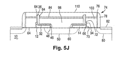
- a protective nitride layer 110 is formed over poly blocks 103 and between oxide blocks 108 in the following manner.
- Nitride is deposited over the structure, followed by a planarizing nitride etch, such as CMP, with oxide blocks 108 used as the etching stop layer, so that nitride layer 110 is level with oxide blocks 108. Nitride layer 109 is also removed by this process. The nitride layer 110 is self aligned to the poly blocks 103 by oxide blocks 108. The resulting structure is shown in Fig. 5H.
- Insulation spacers 74 are then formed adjacent to poly blocks 103 and nitride layer 110, and are made of one or more layers of material. In the preferred embodiment, insulation spacers 74 are made of two layers of material by first depositing a thin layer 76 of oxide, followed by the deposition of a nitride over the structure. An anisotropic nitride etch is performed using oxide layer 76 as an etch stop to remove the deposited nitride except for nitride spacers 78. Ion implantation (e.g.
- N+ is then used to form second regions (terminals) 80 in the substrate in the same manner as the first regions 50 were formed.
- An oxide etch follows, which removes the exposed portions of oxide layer 76.
- a layer of metalized silicon (silicide) 82 is formed in the top of the substrate 10 next to side wall spacers 74, by depositing a metal such as tungsten, cobalt, titanium, nickel, platinum, or molybdenum over the structure. The structure is then annealed, permitting the hot metal to flow and to seep into the exposed top portions of the substrate 10 to form silicide regions 82. The remaining metal deposited on the remaining structure is removed by a metal etch process.
- Metalized silicon region 82 on substrate 10 can be called self aligned silicide (i.e. salicide), because it is self aligned to the second regions 80 by spacers 78.
- the resulting structure is shown in Fig. 5J.
- Passivation such as BPSG 86, is used to cover the entire structure.
- a masking step is performed to define etching areas over the salicide regions 82.
- the BPSG 86 is selectively etched in the masked regions to create contact openings that are ideally centered over and wider than the salicide regions 82 formed between adjacent sets of paired memory cells.
- Nitride layer 110 serves to protect poly blocks 103 and metalized silicon layers 84 from this etch process.
- the contact openings are then filled with a conductor metal by metal deposition and planarizing etch-back, whereby the entire area between nitride spacers 78 of adjacent sets of paired memory cells is filled with the deposited metal to form contact conductors 88 that are self aligned to the salicide regions 82 by the nitride spacers 78 (i.e. self aligned contact scheme, or SAC).
- the salicide layers 82 facilitate conduction between the conductors 88 and second regions 80.
- a bit line 90 is added by metal masking over the BPSG 86, to connect together all the conductors 88 in the column of memory cells.
- the final memory cell structure is illustrated in Fig. 5K.
- the third alternate embodiment has the advantage of combining the advantages of the first alternate embodiment, with the advantages of SAC.
- first trench upper and lower portions need not be symmetrical, but rather the first trenches need only have an indentation in the sidewall thereof so that the source line formed therein has a first portion disposed adjacent to the floating gate, and a second portion disposed over the floating gate.
Abstract
A self aligned method of forming a semiconductor
memory array of floating gate memory cells in a
semiconductor substrate having a plurality of spaced apart
isolation regions and active regions on the substrate
substantially parallel to one another in the column
direction. Floating gates (14) are formed in each of the
active regions. In the row direction, trenches are formed
that include indentations or different widths. The
trenches are filled with a conducting material to form
blocks (96) of the conducting material that constitute
source regions with a first portion (60) that is disposed
adjacent to but insulated from the floating gate (14), and
a second portion (62) that this disposed over but
insulated from the floating gate (14).
Description
- The present invention relates to a self-aligned method of forming a semiconductor memory array of floating gate memory cells of the split gate type. The present invention also relates to a semiconductor memory array of floating gate memory cells of the foregoing type.
- Non-volatile semiconductor memory cells using a floating gate to store charges thereon and memory arrays of such non-volatile memory cells formed in a semiconductor substrate are well known in the art. Typically, such floating gate memory cells have been of the split gate type, or stacked gate type, or a combination thereof.
- One of the problems facing the manufacturability of semiconductor floating gate memory cell arrays has been the alignment of the various components such as source, drain, control gate, and floating gate, especially as the memory cells are scaled down in size. As the design rule of integration of semiconductor processing decreases, reducing the smallest lithographic feature, the need for precise alignment becomes more critical. Alignment of various parts also determines the yield of the manufacturing of the semiconductor products.
- Self-alignment is well known in the art. Self-alignment refers to the act of processing one or more steps involving one or more materials such that the features are automatically aligned with respect to one another in that step processing. Accordingly, the present invention uses the technique of self-alignment to achieve the manufacturing of a semiconductor memory array of the floating gate memory cell type.
- Two major issues are often implicated as memory cell dimensions are scaled down. First, the resistance in the source line increases with smaller memory cell dimensions, and a higher resistance suppresses the desirable cell current during a read event. Second, smaller memory cell dimensions result in a lower punch-through voltage VPT between the source and the bitline junction, which limits the achievable maximum floating-gate voltage Vfg during a program event. Floating-gate voltage Vfg is achieved through voltage coupling from the source region through the coupling oxide layer that is between the source and the floating gate. In a source-side injection mechanism, a higher Vfg (and thus a higher punch-through voltage VPT) is essential for a sufficient hot carrier injection efficiency.
- The present invention solves the above mentioned problems by providing a (T-shaped) source region, where a wider conductive upper portion reduces source line resistance, while a narrower lower portion in the source line facilitates smaller memory cell geometries. The memory cell architecture also facilitates the coupling of source voltage to the floating gate through an oxide on the upper portion of the floating gate, in addition to coupling through the bottom coupling oxide, which enhances the coupling coefficient between the source electrode and the floating gate.
- The present invention is a self-aligned method of forming a semiconductor memory array of floating gate memory cells in a semiconductor substrate, each memory cell having a floating gate, a first terminal, a second terminal with a channel region therebetween, and a control gate. Tthe method includes the steps of:
- a) forming a plurality of spaced apart isolation regions on the substrate which are substantially parallel to one another and extend in a first direction, with an active region between each pair of adjacent isolation regions, the active regions each comprising a first layer of insulation material on the semiconductor substrate and a first layer of conductive material on the first layer of insulation material;
- b) forming a plurality of spaced apart first trenches across the active regions and isolation regions which are substantially parallel to one another and extend in a second direction that is substantially perpendicular to the first direction, each of the first trenches having a side wall with an indentation formed therein;
- c) filling each of the first trenches with a conductive material to form first blocks of
conductive material, wherein for each of the first blocks in each active region:
- the first block includes a lower portion formed below the indentation of the first trench sidewall that is disposed adjacent to and insulated from the first layer of conductive material, and
- the first block includes an upper portion formed above the indentation of the first trench sidewall that is disposed over and insulated from the first layer of conductive material;
- d) forming a plurality of first terminals in the substrate, wherein in each of the active regions each of the first terminals is adjacent to and electrically connected with one of the first blocks of conductive material; and
- e) forming a plurality of second terminals in the substrate, wherein in each of the active regions each of the second terminals is spaced apart from the first terminals.
-
- In another aspect of the present invention, an electrically programmable and erasable memory device includes a substrate of semiconductor material of a first conductivity type, first and second spaced-apart regions in the substrate of a second conductivity type with a channel region therebetween, a first insulation layer disposed over said substrate, an electrically conductive floating gate disposed over said first insulation layer and extending over a portion of the channel region and over a portion of the first region, and an electrically conductive source region disposed over and electrically connected to the first region in the substrate. The source region has a lower portion that is disposed adjacent to and insulated from the floating gate and an upper portion that is disposed over and insulated from the floating gate.
- In yet one more aspect of the present invention, an array of electrically programmable and erasable memory devices includes: a substrate of semiconductor material of a first conductivity type, spaced apart isolation regions formed on the substrate which are substantially parallel to one another and extend in a first direction with an active region between each pair of adjacent isolation regions, and each of the active regions includes a column of pairs of memory cells extending in the first direction. Each of the memory cell pairs includes a first region and a pair of second regions spaced apart in the substrate having a second conductivity type with channel regions formed in the substrate between the first region and the second regions, a first insulation layer disposed over said substrate including over the channel regions, a pair of electrically conductive floating gates each disposed over the first insulation layer and extending over a portion of one of the channel regions and over a portion of the first region, and an electrically conductive source region disposed over and electrically connected to the first region in the substrate. The source region has a lower portion that is disposed adjacent to and insulated from the pair of floating gates and an upper portion that is disposed over and insulated from the pair of floating gates.
- Other objects and features of the present invention will become apparent by a review of the specification, claims and appended figures.
- FIG. 1A is a top view of a semiconductor substrate used in the first step of the method of present invention to form isolation regions.
- FIG. 1B is a cross sectional view taken along the line 1-1.
- FIG. 1C is a top view of the next step in the processing of the structure of Fig. 1B, in which isolation regions are formed.
- FIG. 1D is a cross sectional view of the structure in Fig. 1C taken along the line 1-1 showing the isolation stripes formed in the structure.
- FIG. 1E is a cross sectional view of the structure in Fig. 1C taken along the line 1-1 showing the two types of isolation regions that can be formed in the semiconductor substrate: LOCOS or shallow trench.
- FIGs. 2A-2N are cross sectional views taken along the line 2-2 of Fig. 1C showing in sequence the next step(s) in the processing of the structure shown in Fig. 1C, in the formation of a non volatile memory array of floating memory cells of the split gate type.
- FIG. 20 is a top view showing the interconnection of row lines and bit lines to terminals in active regions in the formation of the non volatile memory array of floating memory cells of the split gate type.
- FIGs. 3A-3I are cross sectional views taken along the line 2-2 of Fig. 1C showing in sequence the steps in a first alternate processing of the structure shown in Fig. 1C, in the formation of a non volatile memory array of floating memory cells of the split gate type.
- FIGs. 4A-4J are cross sectional views taken along the line 2-2 of Fig. 1C showing in sequence the steps in a second alternate processing of the structure shown in Fig. 1C, in the formation of a non volatile memory array of floating memory cells of the split gate type.
- FIGs. 5A-5K are cross sectional views taken along the line 2-2 of Fig. 1C showing in sequence the steps in a third alternate processing of the structure shown in Fig. 1C, in the formation of a non volatile memory array of floating memory cells of the split gate type.
- Referring to Fig. 1A there is shown a top plan view of a
semiconductor substrate 10, which is preferably of P type and is well known in the art. A first layer ofinsulation material 12, such as silicon dioxide (oxide), is deposited thereon as shown in Fig. 1B. Thefirst insulation layer 12 is formed on thesubstrate 10 by well known techniques such as oxidation or deposition (e.g. chemical vapor deposition or CVD), forming a layer of silicon dioxide (hereinafter "oxide"). A first layer of polysilicon 14 (FG poly) is deposited on top of the first layer ofinsulation material 12. The deposition and formation of thefirst polysilicon layer 14 on thefirst insulation layer 12 can be made by a well known process such as Low Pressure CVD or LPCVD. A silicon nitride layer 18 (hereinafter "nitride") is deposited over thepolysilicon layer 14, preferably by CVD. Thisnitride layer 18 is used to define the active regions during isolation formation. Of course, all of the forgoing described parameters and the parameters described hereinafter, depend upon the design rules and the process technology generation. What is described herein is for the 0.18 micron process. However, it will be understood by those skilled in the art that the present invention is not limited to any specific process technology generation, nor to any specific value in any of the process parameters described hereinafter. - Once the
first insulation layer 12, thefirst polysilicon layer 14, and thesilicon nitride 18 have been formed, suitable photo-resistant material 19 is applied on thesilicon nitride layer 18 and a masking step is performed to selectively remove the photo-resistant material from certain regions (stripes 16). Where the photo-resistmaterial 19 is removed, thesilicon nitride 18, thepolysilicon 14 and theunderlying insulation material 12 are etched away instripes 16 formed in the Y direction or the column direction, as shown in Fig. 1C, using standard etching techniques (i.e. anisotropic etch process). The distance W betweenadjacent stripes 16 can be as small as the smallest lithographic feature of the process used. Where the photo resist 19 is not removed, thesilicon nitride 18, thefirst polysilicon region 14 and theunderlying insulation region 12 are maintained. The resulting structure is illustrated in Fig. 1D. As will be described, there are two embodiments in the formation of the isolation regions: LOCOS and STI. In the STI embodiment, the etching continues into thesubstrate 10 to a predetermined depth. - The structure is further processed to remove the remaining photo resist 19. Then, an
isolation material nitride layer 18 is then selectively removed to form the structure shown in Fig. 1E. The isolation can be formed via the well known LOCOS process resulting in thelocal field oxide 20a (e.g. by oxidizing the exposed substrate), or it can be formed via a shallow trench process (STI) resulting in silicon-dioxide being formed in theregion 20b (e.g. by depositing an oxide layer, followed by a Chemical-Mechanical-Polishing or CMP etch). It should be noted that during the LOCOS formation, a spacer may be necessary to protect the side walls ofpoly layer 14 during the formation of the local field oxide. - The remaining
first polysilicon layer 14 and the underlyingfirst insulation material 12 form the active regions. Thus, at this point, thesubstrate 10 has alternating stripes of active regions and isolation regions with the isolation regions being formed of eitherLOCOS insulation material 20a or shallowtrench insulation material 20b. Although Fig. 1E shows the formation of both aLOCOS region 20a and ashallow trench region 20b, only one of the LOCOS process (20a) or the shallow trench process (20b) will be used. In the preferred embodiment, theshallow trench 20b will be formed.Shallow trench 20b is preferable because it can be more precisely formed at smaller design rules. - The structure in Fig. 1E represents a self aligned structure, which is more compact than a structure formed by a non self-aligned method. A non self-aligned method of forming the structure shown in Figure 1E, which is well known and is conventional, is as follows. Regions of
isolation 20 are first formed in thesubstrate 10. This can be done by depositing a layer of silicon nitride on thesubstrate 10, depositing photo-resist, patterning the silicon nitride using a first masking step to expose selective portions of thesubstrate 10, and then oxidizing the exposedsubstrate 10 using either the LOCOS process or the STI process where silicon trench formation and trench fill are involved. Thereafter, the silicon nitride is removed, and a first layer of silicon dioxide 12 (to form the gate oxide) is deposited over thesubstrate 10. A first layer ofpolysilicon 14 is deposited over thegate oxide 12. The first layer ofpolysilicon 14 is then patterned using a second masking step and selective portions removed. Thus, thepolysilicon 14 is not self aligned with the regions ofisolation 20, and a second masking step is required. Further, the additional masking step requires that the dimensions of thepolysilicon 14 have an alignment tolerance with respect to the regions ofisolation 20. It should be noted that the non self-aligned method does not utilizenitride layer 18. - With the structure shown in Fig. 1E made using either the self aligned method or the non self-aligned method, the structure is further processed as follows. Referring to Fig. 2A, which shows the structure from a view orthogonal to that of Figs. 1B and 1E, the next steps in the process of the present invention are illustrated. A
thick insulation layer 24, such as silicon nitride (hereinafter "nitride") is formed on the structure, followed by the formation of a thinprotective layer 26 such as polysilicon (hereinafter "poly"). The resulting structure is illustrated in Fig. 2A. - A conventional photo-lithography masking operation is performed with photo-resist applied on top of the
poly layer 26. A masking step is applied in which stripes (i.e. masking regions) are defined in the X or the row direction. The distance between adjacent stripes can be a size determined by the needs of the device to be fabricated. The photo resist is removed in defined masking regions, i.e. stripes in the row direction, after whichpoly layer 26 underlying the removed photo resist is etched away in the stripes using a conventional anisotropic poly etch process to expose portions of theunderlying nitride layer 24. An anisotropic nitride etch process is then performed to remove the exposed portions ofnitride layer 24 to expose portions ofpoly layer 14. An optional poly etch process can follow to remove just a top portion of the exposedpoly layer 14, to slightly recesspoly layer 14 relative to the remainingnitride layer 24, and to form slopedportions 28 ofpoly layer 14 where it meetsnitride layer 24. For each such pair of mirror memory cells, these etch processes result in the formation of a singlefirst trench 30 that extends down to (and preferably slightly into)polysilicon layer 14. The remaining photo-resist is then removed, resulting in the structure shown in Fig. 2B. - A
layer 32 of insulation material, such as silicon dioxide (hereinafter "oxide") is then formed over the structure using, for example, a thermal oxidation process. The portions ofoxide layer 32 formed onpoly layer 14 intrenches 30 have raisedportions 34 caused by slopedportions 28 ofpoly layer 14, givingoxide layer 32 inside trenches 30 a lens shape. The resulting structure is illustrated in Fig. 2C. -
Insulation spacers 40 are then formed inside trenches 30 (Fig. 2E). Formation of spacers is well known in the art by depositing a material over the contour of a structure, followed by an anisotropic etch process (e.g. RIE), whereby the material is removed from horizontal surfaces of the structure, while the material remains largely intact on vertically oriented surfaces of the structure.Spacers 40 can be formed of any dielectric material. In the preferred embodiment, spacers 40 are formed of nitride in the following manner. Athin layer 36 of insulation material (i.e. oxide) is formed over the structure of Fig. 2C preferably using a conventional chemical vapor deposition (CVD) process. Athick layer 38 of insulation material (i.e. nitride) is then formed over the structure preferably by a conventional nitride deposition process, as shown in Fig. 2D. This is followed by a thick nitride etch process that usesoxide layer 36 as an etch stop. This etch process removes all ofnitride layer 38, except forsidewall spacers 40 along the sidewalls oftrenches 30. An anisotropic oxide etch process is then performed that usespoly layer 26 as an etch stop. This oxide etch removes exposed portions ofoxide layers nitride layer 24. The oxide etch also removes portion ofoxide layers trenches 30 betweenspacers 40, to expose portions ofpoly layer 14 at the centers of thetrenches 30. The resulting structure is shown in Fig. 2E. - A thick nitride etch process is performed to remove
spacers 40 fromtrenches 30. A poly etch process is then performed to removepoly layer 26 to exposenitride layer 24, and to remove the exposed portions ofpoly layer 14 at the bottom center oftrenches 30 to exposeoxide layer 12. As shown in Fig. 2F,trenches 30 each have a narrowlower portion 42 bounded bypoly layer 14 andoxide layers wider portion 44 bounded byoxide layer 36. It should be noted that thespacers 40 can be removed after the poly etch process that removes portions ofpoly layer 14. - Suitable ion implantation is made across the entire surface of the structure. Where the ions have sufficient energy to penetrate the first
silicon dioxide layer 12 intrench 30, they then form a first region (terminal) 50 in thesubstrate 10. In all other regions, the ions are absorbed by the existing structure, where they have no effect. Insulation spacers 46 (e.g. oxide) are formed on sidewalls of thelower portions 42 oftrenches 30. Preferably,oxide spacer 46 formation is preceded by first forming an insulation sidewall layer 48 (oxide) on the sides ofpolysilicon layer 14 that are exposed inside trenches 30 (i.e. by oxidizing the structure or by CVD). Then, oxide is formed over the structure (i.e. CVD process), followed by an oxide anisotropic etch, which removes the oxide formed over the structure, except foroxide spacers 46 formed on the sidewalls oflower trench portion 42. This oxide formation and etch process also adds to the thickness of the vertical portion ofoxide layer 36 inupper trench portion 44. The anisotropic etch also removes a top portion ofoxide layer 36, thins down the portion ofoxide layer 36 overoxide layer 32, as well as removes the portion ofoxide layer 12 at the bottom oftrenches 30 in betweenspacers 46 to expose thesubstrate 10. The resulting structure is shown in Fig. 2G. - A
conductive layer 52, such as titanium nitride which adheres well to the exposedsubstrate 10, is formed over the entire structure, which lines the sidewalls oftrenches 30 and exposedsubstrate 10 therein. This is followed by the formation ofconductive blocks 54 insidetrenches 30, which are formed by depositing a conductive material such as tungsten over the structure, followed by a tungsten planarization process (preferably CMP), to filltrenches 30 withconductive blocks 54. A tungsten etch-back step follows to remove any tungsten outside oftrenches 30, and to preferably define the top surfaces ofconductive blocks 54 below the tops of oxide layers 36. A conductive layer 56 (titanium nitride) is then formed overconductive blocks 54, preferably by depositing titanium nitride over the structure, followed by a planarizing (CMP) process that removes the deposited titanium nitride except for theconductive layer 56 overconductive blocks 54 intrenches 30. A titanium nitride etch is then performed so thatconductive layer 56 is recessed below the top ofoxide layer 36. Alayer 58 of insulation material (oxide) is then formed over the structure, followed by a planarization process (CMP) and oxide etch process to remove the deposited oxide except for that portion overconductive layer 56. The resulting structure is shown in Fig. 2H, where the narrow/wide trench portions 42/44 result in substantially T-shaped tungstenconductive blocks 54 with narrowlower block portions 60 and widerupper block portions 62, which are surrounded by titanium nitride layers 52/56. -
Second trenches 63 are formed between pair sets of memory cells and adjacent tofirst trenches 30 in the following manner.Nitride layer 24 is removed, preferably using an isotropic etch process, to expose portions ofpoly layer 14 andoxide layer 32 as shown in Fig. 2I. A poly etch process follows (i.e. a dry etch) to remove exposed portions ofpoly layer 14 and to exposeoxide layer 12. The exposed portions ofoxide layer 12 are then removed via a controlled oxide etch, exposingsubstrate 10. Aninsulation layer 64, preferably oxide, is then formed over the entire structure, resulting in the structure shown in Fig. 2J. The raisedportions 34 ofoxide layer 32 result in the formation of upwardly extendingsharp edges 66 ofpoly layer 14 wherelayer 14 meetsoxide layer 64. - Control gate poly blocks are formed in
second trenches 63 in the following manner. A thick layer of polysilicon is deposited over the structure, followed by an anisotropic poly etch process, which removes all the deposited polysilicon except for poly spacers (blocks) 68 formed against vertically oriented portions ofoxide layer 64. Poly blocks 68 havelower portions 70 disposed immediately adjacent topoly layer 14, andupper portions 72 that extend over a portion of thepoly layer 14 includingsharp edge 66. Poly blocks 68 are insulated frompoly layer 14 byoxide layers -
Insulation spacers 74 are then formed adjacent to poly blocks 68, and are made of one or more layers of material. In the preferred embodiment,insulation spacers 74 are made of two layers of material by first depositing athin layer 76 of oxide, followed by the deposition of nitride over the structure. An anisotropic nitride etch is performed to remove the deposited nitride, leavingnitride spacers 78. Ion implantation (e.g. N+) is then used to form second regions (terminals) 80 in the substrate in the same manner as thefirst regions 50 were formed. A controlled oxide etch follows, which removes the exposed portions ofoxide layer 76, as well as the exposed portions ofoxide layer 64 to exposesubstrate 10 and thesecond regions 80. The resulting structure is shown in Fig. 2L. - A layer of metalized silicon (silicide) 82 is formed in the top of the
substrate 10 next toside wall spacers 74, along with a layer of metalizedsilicon 84 over poly blocks 68, by depositing a metal such as tungsten, cobalt, titanium, nickel, platinum, or molybdenum over the structure. The structure is then annealed, permitting the hot metal to flow and to seep into the exposed top portions of the substrate to formsilicide 82, and into the exposed top portions of poly blocks 68 to form metalizedsilicon 84. The metal deposited on the remaining structure is removed by a metal etch process.Metalized silicon region 82 onsubstrate 10 can be called self aligned silicide (i.e. salicide), because it is self aligned to thesecond regions 80 byspacers 78. The resulting structure is shown in Fig. 2M. - Passivation, such as
BPSG 86, is used to cover the entire structure. A masking step is performed to define etching areas over thesilicide regions 82. TheBPSG 86 is selectively etched in the masked regions to create contact openings that are ideally centered over and extend down tosilicide regions 82 formed between adjacent sets of paired memory cells. The contact openings are then filled with a conductor metal by metal deposition and planarization etch-back to formcontact conductors 88. The silicide layers 82 facilitate conduction between theconductors 88 andsecond regions 80. Abit line 90 is added by metal masking over theBPSG 86, to connect together all theconductors 88 in the column of memory cells. The final memory cell structure is illustrated in Fig. 2N. - As shown in Fig. 2N, first and
second regions 50/80 form the source and drain for each cell (those skilled in the art know that source and drain can be switched during operation). Thechannel region 92 for each cell is the portion of the substrate that is in-between the source and drain 50/80. Poly blocks 68 constitute the control gate, andpoly layer 14 constitutes the floating gate. Oxide layers 32, 36, 46 and 48 together form an insulation layer that is disposed adjacent to and over floatinggate 14, to isolate it fromsource 96. Oxide layers 36 and 64 together form an insulation layer that isolates the source lines 96 from thecontrol gates 68. Thecontrol gates 68 have one side aligned to the edge of thesecond region 80, and are disposed over part of thechannel regions 92.Control gates 68 havelower portions 70 that are disposed adjacent to the floating gates 14 (insulated therefrom by oxide layer 64), and upper protrudingportions 72 that are disposed (extend) over a portion of adjacent poly layers 14 (insulated therefrom by oxide layers 64). A notch 94 is formed by the protrudingportion 72, where thesharp edge 66 of floatinggate 14 extends into the notch 94. Each floatinggate 14 is disposed over part of thechannel region 92, is partially overlapped at one end by thecontrol gate 68, and partially overlaps thefirst region 50 with its other end. Conductive blocks 54 and theconductive layers 52/56 together form source lines 96 that extend across the columns of memory cells.Upper portions 62 ofsource lines 96 extend over but are insulated from the floatinggates 14, whilelower portions 60 ofsource lines 96 are adjacent to but insulated from floatinggates 14. As illustrated in the Fig. 2N, the process of the present invention forms pairs of memory cells that mirror each other. The pairs of mirrored memory cells are insulated from other cell pairs byoxide layer 76,nitride spacers 78 andBPSG 86. - Referring to Fig. 20, there is shown a top plan view of the resulting structure and the interconnection of the bit lines 90 to the
second regions 80, of thecontrol lines 68 which run in the X or the row direction, and of the source lines 96 which connect to thefirst regions 50 within thesubstrate 10. Although the source lines 96 (as should be understood by those skilled in the art, the word "source" is interchangeable with the word "drain") make contact with thesubstrate 10 in the entire row direction, i.e. contact with the active regions as well as the isolation regions, the source lines 96 electrically connect only to thefirst regions 50 in thesubstrate 10. In addition, eachfirst region 50 to which the "source"line 96 is connected is shared between two adjacent memory cells. Similarly, eachsecond region 80 to which thebit line 90 is connected is shared between adjacent memory cells from different mirror sets of memory cells. - The result is a plurality of non volatile memory cells of the split gate type having a floating
gate 14, acontrol gate 68 which is immediately adjacent to but separated from the floatinggate 14 and runs along the length of the row direction connecting to the control gates of other memory cells in the same row, asource line 96 which also runs along the row direction, connecting pairs of thefirst regions 50 of the memory cells in the same row direction, and abit line 90 which runs along the column or Y direction and connects pairs of thesecond regions 80 of the memory cells in the same column direction. The formation of the control gate, the floating gate, the source line, and the bit line, are all self-aligned. The non-volatile memory cell is of the split gate type having floating gate to control gate tunneling all as described in U.S. Patent No. 5,572,054, whose disclosure is incorporated herein by reference with regard to the operation of such a non-volatile memory cell and an array formed thereby. - The present invention exhibits reduced source line resistance because of the wider
upper portion 62 of T-shapedconductive block 52, while still providing for smaller scaling of memory cell dimensions due to the narrowerlower portions 60 of T-shaped conductive blocks 52 (i.e. the indentation of the sidewalls of thefirst trenches 30 between upper andlower portions 62/60 that forms the T-shape of the source line). Theupper portions 62 also extend over but are insulated from the floatinggates 14 which allows coupling of source voltage from thesource line 96 to the floatinggates 14 through the oxide layers 32/36 (which is in addition to the coupling via thelower portions 60 throughoxide layers 46/48, and viafirst region 50 through oxide layer 12). Thus, the coupling coefficient between the source electrode and the floating gate is enhanced. - Figures 3A-3I illustrate a first alternate process for forming a memory cell array similar to that illustrated in Fig. 2N, but with a polysilicon source line. This first alternate process begins with the same structure as shown in Fig. 2G, but continues as follows.
- Conductive blocks 98 are formed inside
trenches 30, preferably by depositing a conductive material such as polysilicon over the structure, followed by a poly planarization process (preferably CMP) to remove polysilicon abovetrenches 30. A poly etch-back step follows to remove any polysilicon outside oftrenches 30, and to recess the top surfaces ofconductive blocks 98 below the tops of oxide layers 36. The poly blocks 98 can be in-Situ doped or doped using implantation. Alayer 58 of insulation material (oxide) is then formed over poly blocks 98, for example by thermal oxidation, or by oxide deposition followed by a CMP planarization process and an oxide etch process so thatoxide layer 58 is recessed below the top ofoxide layer 36. The resulting structure is shown in Fig. 3A, where the narrow/wide trench portions 42/44 result in substantially T-shaped conductive poly blocks 98 with narrowlower block portions 60 and widerupper block portions 62. -
Second trenches 63 are formed between pair sets of memory cells and adjacent tofirst trenches 30 in the following manner.Nitride layer 24 is removed, preferably using an isotropic etch process, to expose portions ofpoly layer 14 andoxide layer 32 as shown in Fig. 3B. A poly etch process follows (i.e. a dry etch) to remove exposed portions ofpoly layer 14 and to expose portions ofoxide layer 12. The exposed portions ofoxide layer 12 are then removed via a controlled oxide etch, exposingsubstrate 10. Aninsulation layer 64, preferably oxide, is then formed over the entire structure, resulting in the structure shown in Fig. 3C. The raisedportions 34 ofoxide layer 32 result in the formation of upwardly extendingsharp edges 66 ofpoly layer 14 wherelayer 14 meetsoxide layer 64. - Control gate poly blocks are formed in
second trenches 63 in the following manner. A thick layer of polysilicon is deposited over the structure, followed by an anisotropic poly etch process, which removes all the deposited polysilicon except for poly spacers (blocks) 68 formed against vertically oriented portions ofoxide layer 64. Poly blocks 68 havelower portions 70 disposed immediately adjacent topoly layer 14, andupper portions 72 that extend over a portion of the poly layers 14 including sharp edges 66. Poly blocks 68 are insulated frompoly layer 14 byoxide layers - An oxide etch is performed to remove exposed portions of
oxide layer 64, and theunderlying oxide layer 58, to exposepoly blocks 98 andsubstrate 10. Preferably, a dry-etch process with end-point detection is used, which also removes the upper portions ofoxide layer 36, so that it is substantially even with the top surface of poly blocks 98. An oxide deposition process follows to form anoxide layer 100 over the structure, and to replaceoxide layer 64 over thesubstrate 10. The resulting structure is illustrated in Fig. 3E. -
Insulation spacers 74 are then formed adjacent to poly blocks 68, and are made of one or more layers of material. In the preferred embodiment,insulation spacers 74 are composite spacers that include lower portions ofoxide layer 100 andnitride spacers 78 formed by the deposition of nitride over the structure followed by an anisotropic nitride etch to remove the deposited nitride (using theoxide layer 100 as an etch stop), leavingnitride spacers 78 overoxide layer 64 and adjacent topoly spacers 68.Nitride spacers 101 are also formed over the ends ofconductive blocks 98, as shown in Fig. 3F. - Ion implantation (e.g. N+) is then used to form second regions (terminals) 80 in the substrate in the same manner as the
first regions 50 were formed. A controlled oxide etch follows to remove the exposed portions ofoxide layer 100 to expose poly blocks 98, and to remove exposed portions ofoxide layer 64 to expose thesubstrate 10. The resulting structure is shown in Fig. 3G. - A layer of metalized silicon (silicide) 82 is formed in the top of the
substrate 10 next toside wall spacers 74, along with a layer of metalizedsilicon 84 over poly blocks 68 andpoly block 98, by depositing a metal such as tungsten, cobalt, titanium, nickel, platinum, or molybdenum over the structure. The structure is then annealed, permitting the hot metal to flow and to seep into the exposed top portions of the substrate to formsilicide 82, and into the exposed top portions of poly blocks 68 and 98 to form metalizedsilicon 84. The metal deposited on the remaining structure is removed by a metal etch process.Metalized silicon region 82 onsubstrate 10 can be called self aligned silicide (i.e. salicide), because it is self aligned to thesecond regions 80 byspacers 78. The resulting structure is shown in Fig. 3H. - Passivation, such as
BPSG 86, is used to cover the entire structure. A masking step is performed to define etching areas over thesilicide regions 82. TheBPSG 86 is selectively etched in the masked regions to create contact openings that are ideally centered over and extend down tosilicide regions 82 formed between adjacent sets of paired memory cells. The contact openings are then filled with a conductor metal by metal deposition and planarization etch-back to formcontact conductors 88. The silicide layers 82 facilitate conduction between theconductors 88 andsecond regions 80. Abit line 90 is added by metal masking over theBPSG 86, to connect together all theconductors 88 in the column of memory cells. The final memory cell structure is illustrated in Fig. 3I. - The first alternate embodiment exhibits reduced source line resistance because of the wider
upper portion 62 of T-shapedpoly block 98 and the highly conductivemetalized silicon layer 84 formed thereon, while still providing for smaller scaling of memory cell dimensions due to the narrowerlower portion 60 of T-shapedconductive block 98. Theupper portions 62 also extend over the floatinggate 14 which allows coupling of source voltage from thepoly block 98 to the floatinggate 14 through the oxide layers 32/36 (in addition to the coupling through the oxide layers 46/48 vialower portions 60, and through theoxide layer 12 via first region 50). Thus, the coupling coefficient between the source electrode and the floating gate is enhanced. - Figures 4A-4I illustrate a second alternate process for forming a memory cell array similar to that illustrated in Fig. 2N, but utilizing a self aligned contact scheme. This second alternate process begins with the same structure as shown in Fig. 2J, but continues as follows.
- A
thick layer 102 of conductive material, such as polysilicon, is deposited over the structure, as shown in Fig. 4A. A layer ofnitride 104 is then deposited over the structure, followed by a nitride planarization process (e.g. CMP). A nitride etch-back step follows to remove the portions ofnitride layer 104 over the raised portions ofpoly layer 102, while leaving portions ofnitride layer 104 over the flat side portions ofpoly layer 102. An oxidation step follows, which oxidizes the exposed center portions ofpoly layer 102 to form a layer ofoxide 106 thereover. The resulting structure is shown in Fig. 4B. -
Nitride layer 104 is removed by a nitride etch process, which is followed by an anisotropic poly etch step to remove those portions ofpoly layer 102 not directly underoxide layer 106, as illustrated in Fig. 4C. - An oxide deposition step is then performed to apply a thick oxide layer over the structure. This is followed by a planarizing oxide etch, such as CMP, to planarize the structure using
poly layer 102 as an etch stop. An oxide etch-back step is then performed, leavingblocks 108 of oxide on either side of thepoly layer 102.Oxide layer 106 is also removed by the oxide planarizing and etch-back steps, resulting in the structure shown in Fig. 4D. A planarizing poly etch, such as CMP, is then performed using the oxide blocks 108 as an etch stop, as illustrated in Fig. 4E. This is followed by a poly etch-back process, such as RIE, to remove the top portions ofpoly layer 102 leaving just poly blocks 103 adjacent oxide blocks 108, and exposingoxide layer 64. Poly blocks 103 havelower portions 70 disposed immediately adjacent topoly layer 14, andupper portions 72 that extend over a portion of thepoly layer 14 includingsharp edge 66. Poly blocks 103 are insulated frompoly layer 14 byoxide layers oxide layer 36 are left to extend well above the top surface of poly blocks 103, as illustrated in Fig. 4F. - An optional implant step can be performed to dope the exposed poly blocks 103. A metal deposition step is then performed, to deposit a metal such as tungsten, cobalt, titanium, nickel, platinum, or molybdenum over the structure. The structure is then annealed, permitting the hot metal to flow and to seep into the exposed top portions of the poly blocks 103 to form a conductive layer of metalized
silicon 84 thereon. The metal deposited on the remaining structure is removed by a metal etch process.Metalized silicon layer 84 can be called self aligned because it is self aligned to the poly blocks 103 byoxide layer 64 and oxide blocks 108. Aprotective nitride layer 110 is formed over poly blocks 103 and betweenoxide blocks 108 in the following manner. Nitride is deposited over the structure, followed by a planarizing nitride etch, such as CMP, withoxide blocks 108 used as the etching stop layer, so thatnitride layer 110 is level with oxide blocks 108. Thenitride layer 110 is self aligned to the poly blocks 103 by oxide blocks 108. The resulting structure is shown in Fig. 4G. - An oxide etch follows to remove
oxide blocks 108 and exposed portions ofoxide layer 64, as illustrated in Fig. 4H.Insulation spacers 74 are then formed adjacent topoly blocks 103 andnitride layer 110, and are made of one or more layers of material. In the preferred embodiment,insulation spacers 74 are made of two layers of material by first depositing athin layer 76 of oxide, followed by the deposition of a nitride over the structure. An anisotropic nitride etch is performed to remove the deposited nitride, leavingnitride spacers 78. Ion implantation (e.g. N+) is then used to form second regions (terminals) 80 in the substrate in the same manner as thefirst regions 50 were formed. An oxide etch follows, which removes the exposed portions ofoxide layer 76. A layer of metalized silicon (silicide) 82 is formed in the top of thesubstrate 10 next toside wall spacers 74, by depositing a metal such as tungsten, cobalt, titanium, nickel, platinum, or molybdenum over the structure. The structure is then annealed, permitting the hot metal to flow and to seep into the exposed top portions of thesubstrate 10 to formsilicide regions 82. The metal deposited on the remaining structure is removed by a metal etch process.Metalized silicon region 82 onsubstrate 10 can be called self aligned silicide (i.e. salicide), because it is self aligned to thesecond regions 80 byspacers 78. The resulting structure is shown in Fig. 4I. - Passivation, such as
BPSG 86, is used to cover the entire structure. A masking step is performed to define etching areas over thesalicide regions 82. TheBPSG 86 is selectively etched in the masked regions to create contact openings that are ideally centered over and wider than thesalicide regions 82 formed between adjacent sets of paired memory cells.Nitride layer 110 serves to protectpoly blocks 103 and metalizedsilicon 84 from this etch process. The contact openings are then filled with a conductor metal by metal deposition and planarizing etch-back, whereby the entire area betweennitride spacers 78 of adjacent sets of paired memory cells is filled with the deposited metal to formcontact conductors 88 that are self aligned to thesalicide regions 82 by the nitride spacers 78 (i.e. self aligned contact scheme, or SAC). The salicide layers 82 facilitate conduction between theconductors 88 andsecond regions 80. Abit line 90 is added by metal masking over theBPSG 86, to connect together all theconductors 88 in the column of memory cells. The final memory cell structure is illustrated in Fig. 4J. - The self aligned contact scheme (SAC) removes an important constraint on the minimum spacing requirement between adjacent sets of paired memory cells. Specifically, while Fig. 4J illustrates the contact area (and thus conductors 88) perfectly centered over the
salicide regions 82, in reality it is very difficult to form the contact openings without some undesirable horizontal shift relative to thesalicide regions 82. With a non-self aligned contact scheme, where there is no protective layer of nitride over the structure before BPSG formation, electrical shorts can occur if thecontact 88 is shifted over and formed over metalizedsilicon 84 andpoly block 103. To prevent electrical shorts in a non-self aligned contact scheme, the contact openings would have to be formed sufficiently away from thenitride spacers 78 so that even with the maximum possible shift in the contact regions, they will not extend to nitridespacers 78 or beyond. This of course would present a constraint on the minimum distance betweenspacers 78, in order to provide a sufficient tolerance distance between adjacent sets of paired mirror cells. - The SAC method of the present invention eliminates this constraint by using the protective layer of material (nitride layer 110) underneath the BPSG. With this protective layer, the contact openings are formed in the BPSG with a sufficient width to ensure there is overlap of the contact opening with the
salicide regions 82, even if there is a significant horizontal shift of the contact opening during formation.Nitride layer 110 allows portions ofcontact 88 to be formed overpoly block 103 or metalizedsilicon layer 84, without any shorting therebetween. The wide contact opening guarantees thatcontacts 88 completely fill the very narrow spaces betweenspacers 78, and make good electrical contact withsalicide regions 82. Thus, the width of contact regions betweenspacers 78 can be minimized, while preventing faulty connections by filling the space betweenspacers 78, allowing the scaling down of the overall cell dimension. - This second alternate embodiment has the further advantage that control
gates 103 are substantially rectangularly shaped with a protrudingportion 72 over the floatinggate 14, and a planar opposing surface that facilitates the formation ofspacers 74, which in turn facilitates the self aligned formation of thesalicide regions 82, and the formation of the self alignedconductor 88. - Figures 5A-5K illustrate a third alternate process for forming a memory cell array similar to that illustrated in Fig. 3I, but utilizing a self aligned contact scheme. This third alternate process begins with the same structure as shown in Fig. 3C, but continues as follows.
- A
thick layer 102 of conductive material, such as polysilicon, is deposited over the structure, as shown in Fig. 5A. A layer ofnitride 104 is then deposited over the structure, followed by a nitride planarization process (e.g. CMP). A nitride etch-back step follows to remove the portions ofnitride layer 104 over the raised portions ofpoly layer 102, while leaving portions ofnitride layer 104 over the flat side portions ofpoly layer 102. An oxidation step follows, which oxidizes the exposed center portions ofpoly layer 102 to form a layer ofoxide 106 thereover. The resulting structure is shown in Fig. 5B. -
Nitride layer 104 is removed by a nitride etch process, which is followed by an anisotropic poly etch step to remove those portions ofpoly layer 102 not directly underoxide layer 106, as illustrated in Fig. 5C. - An oxide deposition step is then performed to apply a
thick oxide layer 108 over the structure. This is followed by a planarizing oxide etch, such as CMP, to planarize the structure usingpoly layer 102 as an etch stop. An oxide etch-back step is then performed, leavingblocks 108 of oxide on either side of thepoly layer 102.Oxide layer 106 is also removed by the oxide planarizing and etch-back steps. A nitride deposition step is then performed to apply a nitride layer over the structure. This is followed by a planarizing nitride etch, such as CMP, to planarize the structure usingpoly layer 102 as an etch stop. A nitride etch-back step is then performed, leavingnitride layer 109 over oxide blocks 108. The resulting structure is shown in Fig. 5D. - A planarizing poly etch, such as CMP, is then performed using the
nitride layer 109 as an etch stop, as illustrated in Fig. 5E. This is followed by a poly etch-back process, such as RIE, to remove the top portions ofpoly layer 102 leaving just poly blocks 103 adjacent oxide blocks 108, and exposingoxide layer 64. Poly blocks 103 havelower portions 70 disposed immediately adjacent topoly layer 14, andupper portions 72 that extend over a portion of thepoly layer 14 includingsharp edge 66. Poly blocks 103 are insulated frompoly layer 14 byoxide layers oxide layer 36 are left to extend well above the top surface of poly blocks 103, as illustrated in Fig. 5F. - A controlled oxide etch is performed to remove exposed horizontal portions of
oxide layer 64, and theunderlying oxide layer 58, to expose poly blocks 98. Preferably, a dry-etch process with end-point detection is used, which also removes the upper portions ofoxide layer 36, as illustrated in Fig. 5G. - An optional implant step can be performed to dope the exposed poly blocks 103. A metal deposition step is then performed, to deposit a metal such as tungsten, cobalt, titanium, nickel, platinum, or molybdenum over the structure. The structure is then annealed, permitting the hot metal to flow and to seep into the exposed top portions of the poly blocks 103 and 98 to form a conductive layer of metalized
silicon 84 thereon. The metal deposited on the remaining structure is removed by a metal etch process.Metalized silicon layer 84 can be called self aligned because it is self aligned to the poly blocks 103 byoxide layer 64 and oxide blocks 108. Aprotective nitride layer 110 is formed over poly blocks 103 and betweenoxide blocks 108 in the following manner. Nitride is deposited over the structure, followed by a planarizing nitride etch, such as CMP, withoxide blocks 108 used as the etching stop layer, so thatnitride layer 110 is level with oxide blocks 108.Nitride layer 109 is also removed by this process. Thenitride layer 110 is self aligned to the poly blocks 103 by oxide blocks 108. The resulting structure is shown in Fig. 5H. - An oxide etch follows to remove
oxide blocks 108 and exposed portions ofoxide layer 64, as illustrated in Fig. 5I.Insulation spacers 74 are then formed adjacent topoly blocks 103 andnitride layer 110, and are made of one or more layers of material. In the preferred embodiment,insulation spacers 74 are made of two layers of material by first depositing athin layer 76 of oxide, followed by the deposition of a nitride over the structure. An anisotropic nitride etch is performed usingoxide layer 76 as an etch stop to remove the deposited nitride except fornitride spacers 78. Ion implantation (e.g. N+) is then used to form second regions (terminals) 80 in the substrate in the same manner as thefirst regions 50 were formed. An oxide etch follows, which removes the exposed portions ofoxide layer 76. A layer of metalized silicon (silicide) 82 is formed in the top of thesubstrate 10 next toside wall spacers 74, by depositing a metal such as tungsten, cobalt, titanium, nickel, platinum, or molybdenum over the structure. The structure is then annealed, permitting the hot metal to flow and to seep into the exposed top portions of thesubstrate 10 to formsilicide regions 82. The remaining metal deposited on the remaining structure is removed by a metal etch process.Metalized silicon region 82 onsubstrate 10 can be called self aligned silicide (i.e. salicide), because it is self aligned to thesecond regions 80 byspacers 78. The resulting structure is shown in Fig. 5J. - Passivation, such as
BPSG 86, is used to cover the entire structure. A masking step is performed to define etching areas over thesalicide regions 82. TheBPSG 86 is selectively etched in the masked regions to create contact openings that are ideally centered over and wider than thesalicide regions 82 formed between adjacent sets of paired memory cells.Nitride layer 110 serves to protectpoly blocks 103 and metalized silicon layers 84 from this etch process. The contact openings are then filled with a conductor metal by metal deposition and planarizing etch-back, whereby the entire area betweennitride spacers 78 of adjacent sets of paired memory cells is filled with the deposited metal to formcontact conductors 88 that are self aligned to thesalicide regions 82 by the nitride spacers 78 (i.e. self aligned contact scheme, or SAC). The salicide layers 82 facilitate conduction between theconductors 88 andsecond regions 80. Abit line 90 is added by metal masking over theBPSG 86, to connect together all theconductors 88 in the column of memory cells. The final memory cell structure is illustrated in Fig. 5K. - The third alternate embodiment has the advantage of combining the advantages of the first alternate embodiment, with the advantages of SAC.
- It is to be understood that the present invention is not limited to the embodiments described above and illustrated herein, but encompasses any and all variations falling within the scope of the appended claims. For example, although the foregoing method describes the use of appropriately doped polysilicon as the conductive material used to form the memory cells, it should be clear to those having ordinary skill in the art that any appropriate conductive material can be used. In addition, any appropriate insulator can be used in place of silicon dioxide or silicon nitride. Moreover, any appropriate material whose etch property differs from silicon dioxide (or any insulator) and from polysilicon (or any conductor) can be used in place of silicon nitride. Further, as is apparent from the claims, not all method steps need be performed in the exact order illustrated or claimed, but rather in any order that allows the proper formation of the memory cell of the present invention. Finally, the first trench upper and lower portions need not be symmetrical, but rather the first trenches need only have an indentation in the sidewall thereof so that the source line formed therein has a first portion disposed adjacent to the floating gate, and a second portion disposed over the floating gate.
Claims (24)
- A self-aligned method of forming a semiconductor memory array of floating gate memory cells in a semiconductor substrate, each memory cell having a floating gate, a first terminal, a second terminal with a channel region therebetween, and a control gate, the method comprising the steps of:a) forming a plurality of spaced apart isolation regions on the substrate which are substantially parallel to one another and extend in a first direction, with an active region between each pair of adjacent isolation regions, the active regions each comprising a first layer of insulation material on the semiconductor substrate and a first layer of conductive material on the first layer of insulation material;b) forming a plurality of spaced apart first trenches across the active regions and isolation regions which are substantially parallel to one another and extend in a second direction that is substantially perpendicular to the first direction, each of the first trenches having a side wall with an indentation formed therein;c) filling each of the first trenches with a conductive material to form first blocks of conductive material, wherein for each of the first blocks in each active region:the first block includes a lower portion formed below the indentation of the first trench sidewall that is disposed adjacent to and insulated from the first layer of conductive material, andthe first block includes an upper portion formed above the indentation of the first trench sidewall that is disposed over and insulated from the first layer of conductive material;d) forming a plurality of first terminals in the substrate, wherein in each of the active regions each of the first terminals is adjacent to and electrically connected with one of the first blocks of conductive material; ande) forming a plurality of second terminals in the substrate, wherein in each of the active regions each of the second terminals is spaced apart from the first terminals.
- The method of claim 1, wherein the first blocks of conductive material are substantially T-shaped.
- The method of claim 1, further comprising the step of:forming a layer of metalized silicon on each of the first blocks of conductive material.
- The method of claim 1 further comprising the step of:forming a second layer of conductive material in the first trenches before forming the first blocks of conductive material.
- The method of claim 1, further comprising the step of:wherein the lower and upper portions of each of the first blocks are insulated from the first layer of conductive material by the second layer of insulation material.forming a second layer of insulation material along sidewalls of each of the first trenches,
- The method of claim 1, further comprising the step of:forming a plurality of spaced apart second trenches which are substantially parallel to one another and to the first trenches;forming second blocks of a conductive material in the second trenches, wherein for each of the second blocks of conductive material:the second block includes a lower portion that is disposed adjacent to and insulated from the first layer of conductive material, andthe second block includes an upper portion that is disposed over and insulated from the first layer of conductive material.
- The method of claim 6, further comprising the step of:forming a layer of metalized silicon on each of the second blocks of conductive material.
- The method of claim 1, wherein the formation of the first trenches comprises the steps of:wherein the sidewall indentations are formed between the top and bottom portions of the first trenches.forming at least one layer of a first material over the first layer of conductive material, selectively etching through the at least one layer of first material to form the top portions of the first trenches;forming at least one layer of a second material along a bottom surface of the first trenches;forming side wall spacers on side walls of each of the first trenches;etching between the side wall spacers in each of the first trenches and through the at least one layer of second material to expose portions of the first layer of conductive material; andetching the exposed portions of the first layer of conductive material to form the bottom portions of the first trenches;
- The method of claim 6, further comprising the steps of:forming a side wall spacer of insulating material along a side wall of each of the second blocks of conductive material; andforming a layer of metalized silicon on each of the second terminals, wherein each of the layers of metalized silicon is self-aligned to the one of the side wall spacers.
- The method of claim 9, further comprising the step of:forming a conductive material over each of the layers of metalized silicon and against the side wall spacer self aligned thereto.
- The method of claim 9, wherein the formation of each of the side wall spacers includes forming a layer of insulation material between the side wall spacer and the side wall of the second block of conductive material.
- The method of claim 6, further comprising the steps of:forming third blocks of a material in the second trenches and adjacent to the second blocks of conductive material;forming a layer of metalized silicon on each of the second blocks of conductive material, wherein for each of the second trenches, a side wall of one of the third blocks of material aligns an edge of the metalized silicon layer to an edge of the second block of conductive material; andforming a second layer of insulation material over the layer of metalized silicon, wherein for each of the second trenches, the side wall of the one third block of material aligns an edge of the second layer of insulation material to the edge of the metalized silicon and to the edge of the second block of conductive material.
- The method of claim 6, further comprising the steps of:forming a side wall spacer of insulating material along a side wall of each of the second blocks of conductive material such that pairs of the side wall spacers are adjacent to but spaced apart from each other with one of the second terminals substantially therebetween;forming a layer of metalized silicon on each one of the second terminals between a pair of the side wall spacers corresponding to the one second terminal such that the layer of metalized silicon is self-aligned to the one second terminal by the corresponding pair of side wall spacers;forming a layer of protective insulation material over the second blocks of conductive material;forming a layer of passivation material over the active regions;forming contact openings through the passivation material, wherein for each of the contact openings:the contact opening extends down to and exposes one of the metalized silicon layers,the contact opening has a lower portion bounded by the corresponding pair of side wall spacers, andthe contact opening has an upper portion that is wider than a spacing between the corresponding pair of side wall spacers; andfilling each of the contact openings with a conductive material.
- The method of claim 1, wherein:each of the first trenches has an upper portion and a lower portion, the upper portion has a greater width than that of the lower portion;each of the first block lower portions is formed in one of the lower portions of one of the first trenches; andeach of the first block upper portions is formed in one of the upper portions of one of the first trenches.
- An array of electrically programmable and erasable memory devices comprising:a substrate of semiconductor material of a first conductivity type;spaced apart isolation regions formed on the substrate which are substantially parallel to one another and extend in a first direction, with an active region between each pair of adjacent isolation regions; andeach of the active regions including pairs of memory cells extending in the first direction, each of the memory cell pairs including:a first region and a pair of second regions spaced apart in the substrate having a second conductivity type, with channel regions formed in the substrate between the first region and the second regions,a first insulation layer disposed over said substrate including over the channel regions,a pair of electrically conductive floating gates each disposed over the first insulation layer and extending over a portion of one of the channel regions and over a portion of the first region, andan electrically conductive source region disposed over and electrically connected to the first region in the substrate, the source region having a lower portion that is disposed adjacent to and insulated from the pair of floating gates and an upper portion that is disposed over and insulated from the pair of floating gates.
- The device of claim 15, wherein the source region upper portion has a greater width than that of the source region lower portion.
- The device of claim 16, wherein the source region has a substantially T-shaped cross-section.
- The device of claim 15, wherein each of the source regions extends across the active regions and isolation regions in a second direction substantially perpendicular to the first direction and intercepts one of the memory cell pairs in each of the active regions.
- The device of claim 15, wherein each of the memory cell pairs further comprises:a second insulation layer disposed over and adjacent to each of the floating gates and having a thickness permitting Fowler-Nordheim tunneling of charges therethrough; anda pair of electrically conductive control gates each having a first portion and a second portion, the first control gate portion being disposed adjacent to the second insulation layer and one of the floating gates, and the second control gate portion being disposed over a portion of the second insulation layer and a portion of the one floating gate.
- The device of claim 19, wherein each of the control gates extends across the active regions and isolation regions in a second direction substantially perpendicular to the first direction and intercepts one of the memory cell pairs in each of the active regions.
- An electrically programmable and erasable memory device comprising:a substrate of semiconductor material of a first conductivity type;first and second spaced-apart regions in the substrate of a second conductivity type, with a channel region therebetween;a first insulation layer disposed over said substrate;an electrically conductive floating gate disposed over said first insulation layer and extending over a portion of said channel region and over a portion of the first region; andan electrically conductive source region disposed over and electrically connected to the first region in the substrate, the source region having a lower portion that is disposed adjacent to and insulated from the floating gate and an upper portion that is disposed over and insulated from the floating gate.
- The device of claim 21, wherein the source region upper portion has a greater width than that of the source region lower portion.
- The device of claim 22, wherein the source region has a substantially T-shaped cross-section.
- The device of claim 21, further comprising:a second insulation layer disposed over and adjacent the floating gate and having a thickness permitting Fowler-Nordheim tunneling of charges therethrough; andan electrically conductive control gate having a first portion and a second portion, the first control gate portion being disposed adjacent to the second insulation layer and the floating gate, and the second control gate portion being disposed over a portion of the second insulation layer and a portion of the floating gate.
Applications Claiming Priority (12)
| Application Number | Priority Date | Filing Date | Title |
|---|---|---|---|
| US23431400P | 2000-09-20 | 2000-09-20 | |
| US234314P | 2000-09-20 | ||
| US24209600P | 2000-10-19 | 2000-10-19 | |
| US242096P | 2000-10-19 | ||
| US26016701P | 2001-01-05 | 2001-01-05 | |
| US260167P | 2001-01-05 | ||
| US27551701P | 2001-03-12 | 2001-03-12 | |
| US275517P | 2001-03-12 | ||
| US28704701P | 2001-04-26 | 2001-04-26 | |
| US287047P | 2001-04-26 | ||
| US09/916,555 US6727545B2 (en) | 2000-09-20 | 2001-07-26 | Semiconductor memory array of floating gate memory cells with low resistance source regions and high source coupling |
| US916555 | 2001-07-26 |
Publications (1)
| Publication Number | Publication Date |
|---|---|
| EP1191586A2 true EP1191586A2 (en) | 2002-03-27 |
Family
ID=27559246
Family Applications (1)
| Application Number | Title | Priority Date | Filing Date |
|---|---|---|---|
| EP01307993A Withdrawn EP1191586A2 (en) | 2000-09-20 | 2001-09-19 | Floating gate memory and manufacturing method |
Country Status (5)
| Country | Link |
|---|---|
| US (2) | US6727545B2 (en) |
| EP (1) | EP1191586A2 (en) |
| JP (1) | JP5027365B2 (en) |
| KR (1) | KR100855885B1 (en) |
| CN (1) | CN1222992C (en) |
Cited By (1)
| Publication number | Priority date | Publication date | Assignee | Title |
|---|---|---|---|---|
| WO2021002934A1 (en) * | 2019-07-02 | 2021-01-07 | Silicon Storage Technology, Inc. | Method of forming split gate memory cells |
Families Citing this family (52)
| Publication number | Priority date | Publication date | Assignee | Title |
|---|---|---|---|---|
| KR100455379B1 (en) * | 2002-02-21 | 2004-11-06 | 삼성전자주식회사 | Method for fabricating flash memory |
| US6734055B1 (en) * | 2002-11-15 | 2004-05-11 | Taiwan Semiconductor Manufactoring Company | Multi-level (4 state/2-bit) stacked gate flash memory cell |
| KR100823694B1 (en) * | 2002-11-21 | 2008-04-21 | 삼성전자주식회사 | Method of forming a structure of floating gate in a non-volatile memory device |
| KR100481871B1 (en) * | 2002-12-20 | 2005-04-11 | 삼성전자주식회사 | Non-volatile memory cells having floating gate and method of forming the same |
| US6706599B1 (en) * | 2003-03-20 | 2004-03-16 | Motorola, Inc. | Multi-bit non-volatile memory device and method therefor |
| US7183163B2 (en) * | 2003-04-07 | 2007-02-27 | Silicon Storage Technology, Inc. | Method of manufacturing an isolation-less, contact-less array of bi-directional read/program non-volatile floating gate memory cells with independent controllable control gates |
| US7759719B2 (en) * | 2004-07-01 | 2010-07-20 | Chih-Hsin Wang | Electrically alterable memory cell |
| US7550800B2 (en) * | 2003-06-06 | 2009-06-23 | Chih-Hsin Wang | Method and apparatus transporting charges in semiconductor device and semiconductor memory device |
| US7613041B2 (en) * | 2003-06-06 | 2009-11-03 | Chih-Hsin Wang | Methods for operating semiconductor device and semiconductor memory device |
| US7105406B2 (en) * | 2003-06-20 | 2006-09-12 | Sandisk Corporation | Self aligned non-volatile memory cell and process for fabrication |
| US7009244B2 (en) * | 2003-07-02 | 2006-03-07 | Integrated Memory Technologies, Inc. | Scalable flash EEPROM memory cell with notched floating gate and graded source region |
| US6890821B2 (en) | 2003-07-11 | 2005-05-10 | Taiwan Semiconductor Manufacturing Co., Ltd. | Method and system for forming source regions in memory devices |
| US6911704B2 (en) * | 2003-10-14 | 2005-06-28 | Advanced Micro Devices, Inc. | Memory cell array with staggered local inter-connect structure |
| US6960506B2 (en) * | 2003-11-13 | 2005-11-01 | Macronix International Co., Ltd. | Method of fabricating a memory device having a self-aligned contact |
| DE10356285A1 (en) | 2003-11-28 | 2005-06-30 | Infineon Technologies Ag | Integrated semiconductor memory and method for manufacturing an integrated semiconductor memory |
| KR100526478B1 (en) * | 2003-12-31 | 2005-11-08 | 동부아남반도체 주식회사 | Semiconductor device and fabricating method thereof |
| US7315056B2 (en) | 2004-06-07 | 2008-01-01 | Silicon Storage Technology, Inc. | Semiconductor memory array of floating gate memory cells with program/erase and select gates |
| US20080203464A1 (en) * | 2004-07-01 | 2008-08-28 | Chih-Hsin Wang | Electrically alterable non-volatile memory and array |
| KR100591768B1 (en) * | 2004-07-12 | 2006-06-26 | 삼성전자주식회사 | Memory devices and methods for forming the same |
| JP2006032950A (en) * | 2004-07-12 | 2006-02-02 | Samsung Electronics Co Ltd | Memory device and forming method therefor |
| JP2006093707A (en) * | 2004-09-22 | 2006-04-06 | Samsung Electronics Co Ltd | Semiconductor device and manufacturing method therefor |
| KR100621553B1 (en) | 2004-09-22 | 2006-09-19 | 삼성전자주식회사 | Nonvolatile memory device and method for fabricating the same |
| KR100598047B1 (en) * | 2004-09-30 | 2006-07-07 | 삼성전자주식회사 | Device for non-volatile memory and method for fabricating thereof |
| KR100645063B1 (en) * | 2005-03-14 | 2006-11-10 | 삼성전자주식회사 | Non-volatile memory device and method of fabricating the same |
| US7411244B2 (en) | 2005-06-28 | 2008-08-12 | Chih-Hsin Wang | Low power electrically alterable nonvolatile memory cells and arrays |
| US7265013B2 (en) * | 2005-09-19 | 2007-09-04 | International Business Machines Corporation | Sidewall image transfer (SIT) technologies |
| CN100446186C (en) * | 2006-10-09 | 2008-12-24 | 上海华虹Nec电子有限公司 | Floating grid preparation method used for grid dividing structure flash memory |
| US7641226B2 (en) * | 2006-11-01 | 2010-01-05 | Autoliv Development Ab | Side airbag module with an internal guide fin |
| US8138524B2 (en) | 2006-11-01 | 2012-03-20 | Silicon Storage Technology, Inc. | Self-aligned method of forming a semiconductor memory array of floating memory cells with source side erase, and a memory array made thereby |
| US8072023B1 (en) | 2007-11-12 | 2011-12-06 | Marvell International Ltd. | Isolation for non-volatile memory cell array |
| US8120088B1 (en) | 2007-12-07 | 2012-02-21 | Marvell International Ltd. | Non-volatile memory cell and array |
| CN101777519B (en) * | 2010-01-12 | 2013-09-25 | 上海宏力半导体制造有限公司 | Split-gate type nonvolatile storage and production method thereof |
| CN101770991B (en) * | 2010-01-12 | 2013-12-04 | 上海宏力半导体制造有限公司 | Nonvolatile memory of gate-distribution embedding type floating gate and manufacturing method thereof |
| DE102011000818A1 (en) * | 2011-02-18 | 2012-08-23 | United Monolithic Semiconductors Gmbh | Semiconductor component manufacturing method for high-frequency engineering planar structure, involves deriving termination of back etching procedure from detection of reaching interlayer |
| US8711636B2 (en) | 2011-05-13 | 2014-04-29 | Silicon Storage Technology, Inc. | Method of operating a split gate flash memory cell with coupling gate |
| CN103579362B (en) * | 2012-07-30 | 2018-03-27 | 联华电子股份有限公司 | Semiconductor device and preparation method thereof |
| US20140110777A1 (en) | 2012-10-18 | 2014-04-24 | United Microelectronics Corp. | Trench gate metal oxide semiconductor field effect transistor and fabricating method thereof |
| CN102983080B (en) * | 2012-12-26 | 2017-02-08 | 上海华虹宏力半导体制造有限公司 | Method for improving erasure and programming performances of split gate memory |
| US9379121B1 (en) * | 2015-01-05 | 2016-06-28 | Silicon Storage Technology, Inc. | Split gate non-volatile flash memory cell having metal gates and method of making same |
| US10141321B2 (en) * | 2015-10-21 | 2018-11-27 | Silicon Storage Technology, Inc. | Method of forming flash memory with separate wordline and erase gates |
| CN107305892B (en) * | 2016-04-20 | 2020-10-02 | 硅存储技术公司 | Method of forming tri-gate non-volatile flash memory cell pairs using two polysilicon deposition steps |
| CN110021602B (en) | 2018-01-05 | 2023-04-07 | 硅存储技术公司 | Non-volatile memory cell with floating gate in dedicated trench |
| CN110010606B (en) | 2018-01-05 | 2023-04-07 | 硅存储技术公司 | Dual bit non-volatile memory cell with floating gate in substrate trench |
| US10418451B1 (en) | 2018-05-09 | 2019-09-17 | Silicon Storage Technology, Inc. | Split-gate flash memory cell with varying insulation gate oxides, and method of forming same |
| US10838652B2 (en) | 2018-08-24 | 2020-11-17 | Silicon Storage Technology, Inc. | Programming of memory cell having gate capacitively coupled to floating gate |
| US10998325B2 (en) | 2018-12-03 | 2021-05-04 | Silicon Storage Technology, Inc. | Memory cell with floating gate, coupling gate and erase gate, and method of making same |
| CN112185815A (en) | 2019-07-04 | 2021-01-05 | 硅存储技术公司 | Method of forming split gate flash memory cells with spacer defined floating gates and discretely formed polysilicon gates |
| US11017866B2 (en) | 2019-09-03 | 2021-05-25 | Silicon Storage Technology, Inc. | Method of improving read current stability in analog non-volatile memory using final bake in predetermined program state |
| US11309042B2 (en) | 2020-06-29 | 2022-04-19 | Silicon Storage Technology, Inc. | Method of improving read current stability in analog non-volatile memory by program adjustment for memory cells exhibiting random telegraph noise |
| CN113327926B (en) * | 2021-05-27 | 2023-07-04 | 福建省晋华集成电路有限公司 | Dynamic random access memory and manufacturing method thereof |
| US11769558B2 (en) | 2021-06-08 | 2023-09-26 | Silicon Storage Technology, Inc. | Method of reducing random telegraph noise in non-volatile memory by grouping and screening memory cells |
| CN113611745A (en) * | 2021-07-30 | 2021-11-05 | 上海华虹宏力半导体制造有限公司 | Method for manufacturing semiconductor device |
Family Cites Families (33)
| Publication number | Priority date | Publication date | Assignee | Title |
|---|---|---|---|---|
| US5808328A (en) | 1977-02-21 | 1998-09-15 | Zaidan Hojin Handotai Kenkyu Shinkokai | High-speed and high-density semiconductor memory |
| US4757360A (en) | 1983-07-06 | 1988-07-12 | Rca Corporation | Floating gate memory device with facing asperities on floating and control gates |
| US4947221A (en) | 1985-11-29 | 1990-08-07 | General Electric Company | Memory cell for a dense EPROM |
| IT1191566B (en) | 1986-06-27 | 1988-03-23 | Sgs Microelettronica Spa | NON-LABELED SEMICONDUCTOR-TYPE MEMORY DEVICE WITH DOOR NOT CONNECTED (FLOATING GATE) ELECTRICALLY ALTERABLE WITH REDUCED TUNNEL AREA AND MANUFACTURING PROCEDURE |
| US4794565A (en) | 1986-09-15 | 1988-12-27 | The Regents Of The University Of California | Electrically programmable memory device employing source side injection |
| KR910000139B1 (en) | 1986-10-27 | 1991-01-21 | 가부시키가이샤 도시바 | Non-volatile semi-conductor memory device with double gate structure |
| US5268319A (en) | 1988-06-08 | 1993-12-07 | Eliyahou Harari | Highly compact EPROM and flash EEPROM devices |
| JP2600301B2 (en) | 1988-06-28 | 1997-04-16 | 三菱電機株式会社 | Semiconductor memory device and method of manufacturing the same |
| US5051793A (en) | 1989-03-27 | 1991-09-24 | Ict International Cmos Technology, Inc. | Coplanar flash EPROM cell and method of making same |
| KR940006094B1 (en) | 1989-08-17 | 1994-07-06 | 삼성전자 주식회사 | Nonvolatile semiconductor memory device and fabricating method thereof |
| US5029130A (en) | 1990-01-22 | 1991-07-02 | Silicon Storage Technology, Inc. | Single transistor non-valatile electrically alterable semiconductor memory device |
| US5572054A (en) * | 1990-01-22 | 1996-11-05 | Silicon Storage Technology, Inc. | Method of operating a single transistor non-volatile electrically alterable semiconductor memory device |
| US5021848A (en) | 1990-03-13 | 1991-06-04 | Chiu Te Long | Electrically-erasable and electrically-programmable memory storage devices with self aligned tunnel dielectric area and the method of fabricating thereof |
| CA2107676C (en) * | 1991-04-09 | 2000-10-31 | Ping Wang | A single transistor non-volatile electrically alterable semiconductor memory device |
| US5211547A (en) * | 1991-06-17 | 1993-05-18 | Ford Motor Company | Fuel pump and fuel sender assembly |
| JP2815495B2 (en) | 1991-07-08 | 1998-10-27 | ローム株式会社 | Semiconductor storage device |
| US5544103A (en) | 1992-03-03 | 1996-08-06 | Xicor, Inc. | Compact page-erasable eeprom non-volatile memory |
| EP0742956A1 (en) * | 1994-11-28 | 1996-11-20 | National Semiconductor Corporation | High density contactless flash eprom array using channel erase |
| JP3133667B2 (en) | 1995-02-23 | 2001-02-13 | 三洋電機株式会社 | Split gate transistor, method of manufacturing split gate transistor, and nonvolatile semiconductor memory |
| US5780892A (en) | 1995-03-21 | 1998-07-14 | Winbond Electronics Corporation | Flash E2 PROM cell structure with poly floating and control gates |
| KR0144906B1 (en) | 1995-03-31 | 1998-07-01 | 김광호 | Nonvolatile Memory Device and Manufacturing Method Thereof |
| US5597751A (en) | 1995-12-20 | 1997-01-28 | Winbond Electronics Corp. | Single-side oxide sealed salicide process for EPROMs |
| US5814853A (en) | 1996-01-22 | 1998-09-29 | Advanced Micro Devices, Inc. | Sourceless floating gate memory device and method of storing data |
| JP3081543B2 (en) * | 1996-03-29 | 2000-08-28 | 三洋電機株式会社 | Split gate transistor, method of manufacturing split gate transistor, and nonvolatile semiconductor memory |
| JP3342338B2 (en) * | 1996-07-22 | 2002-11-05 | 三洋電機株式会社 | Manufacturing method of nonvolatile semiconductor memory device |
| US5780341A (en) | 1996-12-06 | 1998-07-14 | Halo Lsi Design & Device Technology, Inc. | Low voltage EEPROM/NVRAM transistors and making method |
| US6211547B1 (en) * | 1997-11-24 | 2001-04-03 | Winbond Electronics Corporation | Semiconductor memory array with buried drain lines and processing methods therefor |
| US6140182A (en) | 1999-02-23 | 2000-10-31 | Actrans System Inc. | Nonvolatile memory with self-aligned floating gate and fabrication process |
| US6091104A (en) | 1999-03-24 | 2000-07-18 | Chen; Chiou-Feng | Flash memory cell with self-aligned gates and fabrication process |
| US6103573A (en) | 1999-06-30 | 2000-08-15 | Sandisk Corporation | Processing techniques for making a dual floating gate EEPROM cell array |
| US6222227B1 (en) | 1999-08-09 | 2001-04-24 | Actrans System Inc. | Memory cell with self-aligned floating gate and separate select gate, and fabrication process |
| US6329685B1 (en) * | 1999-09-22 | 2001-12-11 | Silicon Storage Technology, Inc. | Self aligned method of forming a semiconductor memory array of floating gate memory cells and a memory array made thereby |
| US6525371B2 (en) | 1999-09-22 | 2003-02-25 | International Business Machines Corporation | Self-aligned non-volatile random access memory cell and process to make the same |
-
2001
- 2001-07-26 US US09/916,555 patent/US6727545B2/en not_active Expired - Lifetime
- 2001-09-19 JP JP2001284734A patent/JP5027365B2/en not_active Expired - Lifetime
- 2001-09-19 CN CNB011385049A patent/CN1222992C/en not_active Expired - Lifetime
- 2001-09-19 EP EP01307993A patent/EP1191586A2/en not_active Withdrawn
- 2001-09-20 KR KR1020010058313A patent/KR100855885B1/en active IP Right Grant
-
2003
- 2003-10-20 US US10/690,204 patent/US6855980B2/en not_active Expired - Lifetime
Cited By (2)
| Publication number | Priority date | Publication date | Assignee | Title |
|---|---|---|---|---|
| WO2021002934A1 (en) * | 2019-07-02 | 2021-01-07 | Silicon Storage Technology, Inc. | Method of forming split gate memory cells |
| US11081553B2 (en) | 2019-07-02 | 2021-08-03 | Silicon Storage Technology, Inc. | Method of forming split gate memory cells |
Also Published As
| Publication number | Publication date |
|---|---|
| KR20020022630A (en) | 2002-03-27 |
| CN1222992C (en) | 2005-10-12 |
| CN1362736A (en) | 2002-08-07 |
| US20040084717A1 (en) | 2004-05-06 |
| JP5027365B2 (en) | 2012-09-19 |
| JP2002158302A (en) | 2002-05-31 |
| US6727545B2 (en) | 2004-04-27 |
| KR100855885B1 (en) | 2008-09-03 |
| US6855980B2 (en) | 2005-02-15 |
| US20020034849A1 (en) | 2002-03-21 |
Similar Documents
| Publication | Publication Date | Title |
|---|---|---|
| US6855980B2 (en) | Semiconductor memory array of floating gate memory cells with low resistance source regions and high source coupling | |
| US6750090B2 (en) | Self aligned method of forming a semiconductor memory array of floating gate memory cells with floating gates having multiple sharp edges, and a memory array made thereby | |
| US6867082B2 (en) | Nonvolatile memory cells having split gate structure and methods of fabricating the same | |
| EP1087443A2 (en) | Self-aligned non-volatile random access memory cell and process to make the same | |
| KR100821495B1 (en) | Self aligned method of forming a semiconductor memory array of floating gate memory cells with control gate spacers, and a memory array made thereby | |
| US6967372B2 (en) | Semiconductor memory array of floating gate memory cells with vertical control gate sidewalls and insulation spacers | |
| JP2001102467A (en) | Semiconductor memory array of floating gate memory cells, self alignment method forming the same, semiconductor device having array of nonvolatile memory cells, and a plurality of rows connected with a plurality of semiconductor devices | |
| US7351629B2 (en) | Method of forming non-volatile memory device | |
| US6773989B2 (en) | Self aligned method of forming a semiconductor memory array of floating gate memory cells with control gate protruding portions | |
| US6773974B2 (en) | Method of forming a semiconductor array of floating gate memory cells and strap regions | |
| US20040079984A1 (en) | Polysilicon self-aligned contact and a polysilicon common source line and method of forming the same | |
| JP2003100913A (en) | Self-aligning method for forming semiconductor memory array of floating gate memory cell having vertical control gate sidewall and insulation spacer, and memory array formed by the method | |
| US6878591B2 (en) | Self aligned method of forming non-volatile memory cells with flat word line |
Legal Events
| Date | Code | Title | Description |
|---|---|---|---|
| PUAI | Public reference made under article 153(3) epc to a published international application that has entered the european phase |
Free format text: ORIGINAL CODE: 0009012 |
|
| AK | Designated contracting states |
Kind code of ref document: A2 Designated state(s): AT BE CH CY DE DK ES FI FR GB GR IE IT LI LU MC NL PT SE TR |
|
| AX | Request for extension of the european patent |
Free format text: AL;LT;LV;MK;RO;SI |
|
| STAA | Information on the status of an ep patent application or granted ep patent |
Free format text: STATUS: THE APPLICATION HAS BEEN WITHDRAWN |
|
| 18W | Application withdrawn |
Effective date: 20030731 |