TECHNICAL FIELD
-
The present invention relates to an I/O cell placement
method and a semiconductor device using the same.
BACKGROUND
-
In some semiconductor devices which include a
semiconductor chip of silicon or the like where an integrated
circuit is formed, input/output cells (hereinafter called "I/O
cells") which have an interface capability with respect to an
external circuit are arranged along the outer peripheral
portion of the chip. In this case, pads as electrodes to
electrically connect to the external circuit may be placed in
a portion located further outward of the I/O cells. The
individual pads are electrically connected to the
corresponding I/O cells. The I/O cells include a circuit for
connecting the integrated circuit formed in the semiconductor
chip to the external circuit.
-
In case where a semiconductor device is designed in a
gate array, for example, an integrated circuit having desired
functions is realized by connecting basic cells prearranged in
an array form by the interconnects that are correspond with a
circuit designed by a user. At this time, I/O cells likewise
prearranged are connected to the basic cells at the outer
peripheral portion of a semiconductor chip by the interconnects
and the connected I/O cells perform an interface operation with
an external circuit via corresponding pads.
-
Fig. 11 shows one example of the layout of such a
semiconductor chip.
-
This semiconductor device includes a semiconductor chip
10 of silicon or the like, which includes a core transistor
region 12, an I/O cell placement region 14 and a pad placement
region 16.
-
The core transistor region 12 is a region where basic
cells are arranged in an array form in case of, for example,
a gate array. The individual basic cells have their own
functions and provide an operational circuit, which has
obtained a given function by connecting one another with
interconnection.
-
The I/O cell placement region 14 is provided along the
outer periphery of the core transistor region 12 and a plurality
of I/O cells 20 are arranged in the I/O cell placement region
14. The I/O cells 20 include input/output circuits each having
a capability of interfacing a circuit outside the semiconductor
chip 10 with the operational circuit in the core transistor
region 12.
-
The pad placement region 16 is provided along the outer
periphery of the I/O cell placement region 14 and a plurality
of pads 22 are arranged in the pad placement region 16. The pads
22 are electrodes for electrically connecting an external
circuit of the semiconductor chip 10 with the input/output
circuits in the I/O cell placement region 14.
-
Fig. 12 presents an enlarged view of a broken-lined
portion 30 in the semiconductor chip 10 shown in Fig. 11.
-
The I/O cells 20 arranged in the I/O cell placement region
14 have pad connection terminals through which they are
electrically connected to the corresponding pads 22 by
corresponding lead lines 33.
-
Each of the I/O cells 20 includes a driver circuit section
34 and an interface circuit section 36.
-
The driver circuit section 34 has a driver, such as an
input driver or an output driver, and includes an N-type
transistor region 38 and a P-type transistor region 40.
-
The interface circuit section 36 includes a level shifter
circuit, which converts different signal levels, as an
interface circuit between the driver circuit section 34 and the
basic cells formed in the core transistor region 12. In case
where the external circuit operates on a signal level of a
5-volt range and the core transistor region 12 operates on a
signal level of a 3-volt range, the interface circuit section
36 converts the 5-volt range signal level from the external
circuit to a 3-volt range signal level or converts the 3-volt
range signal level from the core transistor region 12 to a
5-volt range signal level.
-
The driver circuit section 34 and the interface circuit
section 36 are electrically connected with a power-supply level
supply line and a ground-level supply line, so that individual
transistors in the N-type transistor region 38 and the P-type
transistor region 40 operate according to the difference
between the potential supplied through the power-supply level
supply line and the potential supplied through the ground-level
supply line.
-
A ground-level supply line 42 which feeds the potential
of the ground level to the driver circuit section 34, a
power-supply level supply line 44 which feeds the potential of
the power-supply level to the driver circuit section 34, and
a power-supply/ground level supply line 46 which feeds the
potentials of the power-supply level and the ground level to
the interface circuit section 36 are placed in the I/O cell
placement region 14. Those supply lines 42, 44 and 46 are
designed by first and second interconnection layers and are
arranged in a ring form on the semiconductor chip 10.
-
To arrange as many pads 22 as possible at the outermost
peripheral portion of the semiconductor chip 10 in such a
semiconductor device, the I/O cells 20 are constructed in
rectangular shapes and are placed in such a manner that their
longitudinal direction (height directions) become
perpendicular to the placement direction of the pads. This
would raise a problem of increasing the area of the
semiconductor chip 10 by the portion corresponding to the
height-directional lengths of the I/O cells.
-
In case where bonding is carried out at the corner
portions of the semiconductor chip 10 as shown in Fig. 12,
particularly, the closer to the chip corner the pads 22 pads
22 are placed, the longer the distance should be taken between
the adjoining pads in order to avoid contact between the bonding
wires connected to the adjoining pads. This requires that the
lead line 33 for electrically connecting such a pad to the
corresponding I/O cell should be bent, thus increasing the area
of the semiconductor chip by the width, d, of the lead line 33.
-
As the width (short length) of the I/O cell would be
defined as the minimum pad pitch, it was not possible to make
the pad pitch narrower. The semiconductor device according to
the related art therefore would face incapability of coping
with the possible increase in the number of pins in the future
diversification of functions.
SUMMARY
-
The present invention has been devised in view of the
above-described technical problems and can provide an I/O cell
placement method and a semiconductor device, which can reduce
the chip area without changing the internal core transistor
region.
-
According to this invention can also provide an I/O cell
placement method and a semiconductor device which can realize
the increase in the number of pins that matches with the future
diversification of functions can be provided, without changing
the internal core transistor region.
-
The present invention relates to an I/O cell placement
method for placing I/O cells which are included in a
semiconductor device electrically connected to a given
external device and have electric interface function with
respect to the external device, the method comprising a step
of placing at least two columns of I/O cells from an outer
peripheral portion of a chip toward a chip core portion in such
a manner that a longitudinal direction of each of the I/O cells
is parallel to an outer peripheral portion.
-
Here, the "given external device" means, for example, an
operational circuit outside the semiconductor device according
to the present invention.
-
The "longitudinal direction" is the longitudinal
direction of an I/O cell which is the direction of the long side
of the I/O cell which is normally constructed in a rectangular
shape, or the so-called height direction of the I/O cell.
-
The outer peripheral portion of the chip indicates the
portion according to the present invention and constitutes the
outer periphery of the semiconductor chip which is included in
the semiconductor device. The chip core portion indicates an
operational circuit region formed in the center portion of the
chip.
-
As plural columns of I/O cells are arranged from the outer
peripheral portion of the chip toward the chip core portion in
such a manner that the height directions of the I/O cells become
parallel to the outer peripheral portion of the chip, it is
possible to improve the degree of freedom of the placement
positions of the pads that are normally restricted not only by
the shapes of the pads but also by the widths of the I/O cells.
This can make it possible to cope with various kinds of packages
without altering the design of the chip core portion.
-
In this invention, a plurality of pads may be placed along
the outer peripheral portion of the chip, and the pads may be
electrically connected to corresponding I/O cells
respectively.
-
While the chip area is inevitably increased by the
portion corresponding to the height direction of the I/O cells
to be placed, plural columns of I/O cells are placed in such
a manner that the longitudinal direction of the I/O cells become
parallel to the placement direction of the pads, so that the
longitudinal-directional length of the I/O cells becomes
shorter than the height-directional length. This can reduce
the area of the chip that has the same functions without
altering the design of the chip core portion.
-
In this invention, the plurality of pads may be placed
at a region closer to a chip core portion than the I/O cells,
and the pads may be electrically connected to corresponding I/O
cells respectively.
-
Here, the placement of the pads in the chip core portion
means the placement of pads in the so-called core transistor
region as in the case of, for example, active surface bumps.
Even in this case, particularly, arranging plural columns of
I/O cells in such a manner that their longitudinal direction
is parallel to the placement direction of the pads. This also
makes it possible to reduce the area of the chip that has the
same functions without altering the design of the chip core
portion.
-
In this invention, when A is a longitudinal length of a
region of the I/O cell and B is another length of a region of
the I/O cell, [A/B] or fewer columns of I/O cells may be placed
in such a manner that longitudinal direction of the I/O cells
are parallel to one another.
-
Here, given that A is the longitudinal length (e.g., the
height direction) of the region of the I/O cell and B is the
other length (e.g., the short-side or width direction), [A/B]
is expressed as the largest integer not exceeding A/B.
-
According to the present invention, if the number of
plural columns of I/O cells is equal to or smaller than [A/B],
it is possible to make the pad pitch wider than that demanded
in the related art and to avoid an increase in the chip area
that is caused by the height-directional length of the I/O cells
or rather reduce the chip area. In view of the point that the
alteration of the design of the chip core portion is unnecessary,
it is possible to effectively achieve cost reduction.
-
In this invention, when A is a longitudinal length of a
region of the I/O cell and B is another length of a region of
the I/O cell, more than [A/B] columns of I/O cells may be placed
in such a manner that longitudinal direction of the I/O cells
are parallel to one another.
-
According to this invention, the placement of more than
[A/B] columns of I/O cells in such a manner that the
longitudinal direction of the I/O cells become parallel to one
another lifts off the limitation on the number of arrangeable
pads that is inevitably put in the related art as the number
of I/O cells becomes large. This brings about a new advantage
that makes it possible to realize the increase in the number
of pins that matches with the future diversification of
functions.
-
According to this invention, each of the I/O cells may
be a plurality of regions including first and second regions
to which first and second power sources are respectively
connected, and the I/O cells may be placed so that the second
region of each of the I/O cells to which the second power source
is connected faces each other when the I/O cells are adjoining
each other in the longitudinal direction.
-
As those regions to which the same power is supplied are
so arranged as to face one another, the power supply line or
the ground line can be shared in addition to the aforementioned
advantage. This improves the degree of freedom of
interconnection and makes the interconnects wider to
effectively take the EMI measures.
-
According to this invention, a level of the second power
source may be a level of power source to be supplied to the chip
core portion, and a level shifter circuit which performs signal
level conversion between a level of the first power source and
a level of the second power source may be located in the second
region to which a level of the second power source is supplied.
-
The present invention can be adapted to a semiconductor
device which is used in a multi-power system and can allow the
semiconductor device to operate on a low voltage, thus reducing
the power consumption.
-
According to this invention, at least layers other than
interconnection layers in the I/O cells may be same in case
where the I/O cells are placed in a first state and in case where
the I/O cells are placed in a second state which is a rotated
first state.
-
According to this invention, as I/O cells can be placed
freely in accordance with the number of pads and the sizes of
the package or the chip core portion, every semiconductor
device can be designed to have the optimal chip size.
Particularly, the provision of sharable I/O cells eliminates
the need to change the design of the chip core portion, so that
a variety of semiconductor devices having the optimal chip
sizes can be developed at a low cost.
-
According to this invention, in the I/O cells, a level
of a power-supply may be supplied through a first
interconnection layer in the first state and a level of the
power-supply may be supplied through a second interconnection
layer connected to the first interconnection layer in the
second state.
-
According to this invention, I/O cells that can be shared
can be adopted even in a multi-power semiconductor device,
making it possible to easily lay annular power lines that can
provide the I/O cells with, for example, the power-supply level
and the ground level.
-
The present invention also relates to a semiconductor
device electrically connected to a given external device,
comprising at least two columns of I/O cells which are placed
from an outer peripheral portion of a chip toward a chip core
portion in such a manner that longitudinal direction of the I/O
cell is parallel to the outer peripheral portion and have an
electric interface function with respect to the external
device.
-
The present invention may include a plurality of pads
placed at a region closer to a chip core portion than the I/O
cells and electrically connected to corresponding I/O cells
respectively.
-
The present invention may include pads placed closer to
the chip core portion than the I/O cells and electrically
connected to corresponding I/O cells.
-
According to this invention, when A is a longitudinal
length of a region of the I/O cell and B is another length, [A/B]
or fewer columns of I/O cells may be placed in such a manner
that longitudinal direction of the I/O cells are parallel to
one another.
-
According to this invention, when A is a longitudinal
length of a region of the I/O cell and B is another length, more
than [A/B] columns of I/O cells may be placed in such a manner
that longitudinal direction of the I/O cells are parallel to
one another.
-
According to this invention, each of the I/O cells may
have a plurality of regions including first and second regions
to which first and second power sources are respectively
connected, and the I/O cells may be placed so that the second
region of each of the I/O cells to which the second power source
is connected faces each other when the I/O cells are adjoining
each other in the longitudinal direction.
-
According to this invention, a level of the second power
source may be a level of power source to be supplied to the chip
core portion, and a level shifter circuit which performs signal
level conversion between a level of the first power source and
a level of the second power source may be located in the second
region to which a level of the second power source is supplied.
BRIEF DESCRIPTION OF THE DRAWINGS
-
- Fig. 1 is an explanatory diagram showing one example of
the layout of a chip of a semiconductor device according to one
embodiment;
- Fig. 2 is a schematic diagram showing a first example of
I/O cells placed on the chip of the semiconductor device
according to the embodiment;
- Fig. 3 is a schematic diagram showing a second example
of I/O cells placed on the chip of the semiconductor device
according to the embodiment;
- Fig. 4 is a structural diagram showing one example of the
circuit structure of an output cell as an I/O cell which is
adapted to the semiconductor device according to the
embodiment;
- Fig. 5 is a circuit structural diagram schematically
illustrating one example of the structure of a prebuffer
circuit;
- Fig. 6 is a circuit structural diagram schematically
illustrating one example of the structure of a first level
shifter circuit;
- Fig. 7 is a circuit structural diagram schematically
illustrating one example of the structure of a second level
shifter circuit;
- Fig. 8 is a circuit structural diagram schematically
illustrating one example of the structure of an output buffer
circuit;
- Fig. 9 is an explanatory diagram showing one example of
the layout of I/O cells arranged laterally in the semiconductor
device according to the embodiment;
- Fig. 10 is an explanatory diagram showing one example of
the layout of I/O cells arranged in a vertically stacked fashion
in the semiconductor device according to the embodiment;
- Fig. 11 is an explanatory diagram showing one example of
the layout of a semiconductor chip as a comparative example;
and
- Fig. 12 is a partly enlarged view of that one example of
the layout of the semiconductor chip as the comparative
example.
-
DETAILED DESCRIPTION
-
The embodiment to be discussed below in no way restricts
the subject matters of the invention recited in the appended
claims. It is to be also noted that not all the structural
elements of the embodiment that will be discussed hereunder are
essential to the invention.
-
One embodiment is elaborated below with reference to the
accompanying drawings.
1. Semiconductor device according to the embodiment
-
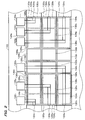
Fig. 1 shows one example of the layout of a chip of a
semiconductor device according to the embodiment.
-
The illustration of the power-supply level supply line
and the ground-level supply line that respectively supply I/O
cells with the power-supply level and the ground level is
omitted.
-
A semiconductor device 100 according to the embodiment
includes a semiconductor chip 110 of silicon or the like.
Unillustrated connection terminals are electrically connected
to the pads of the semiconductor chip 110.
-
The semiconductor chip 110 has a core transistor region
112, an I/O cell placement region 114 and a pad placement region
116.
-
The core transistor region 112 is a region where basic
cells are arranged in an array form in case of, for example,
a gate array. As those basic cells are interconnected together
via an interconnection layer, an operational circuit which is
designed by a user and has a given function is constructed.
-
The I/O cell placement region 114 is provided along the
outer periphery of the core transistor region 112 and a
plurality of I/O cells 120 are place in the I/O cell placement
region 114. The I/O cells 120 include input circuits, output
circuits or input/output circuits each having a capability of
interfacing a circuit outside the semiconductor chip 110 with
the operational circuit in the core transistor region 112. A
power-supply level supply line and a ground-level supply line
that respectively supply the power-supply level and the ground
level to the placed I/O cells 120 are arranged in a ring form
in the I/O cell placement region 114.
-
The pad placement region 116 is provided along the outer
periphery of the I/O cell placement region 114 a plurality of
pads 122 are placed in the pad placement region 116. The pads
122 are electrodes for electrically connecting an external
circuit of the semiconductor chip 110 with the input circuits,
output circuits or input/output circuits in the I/O cell
placement region 114.
-
The semiconductor device 100 according to the embodiment
has a first feature such that at least two columns of I/O cells
120 to be placed in the I/O cell placement region 114 of the
semiconductor chip 110 have rectangular shapes and are placed
in such a manner that the longitudinal direction (height
directions) of the I/O cells become parallel to the placement
direction of the corresponding pads (the direction parallel to
the outer peripheral portion of the chip) and are stacked in
a direction perpendicular to the placement direction of the
pads.
-
Fig. 2 schematically shows a first example of I/O cells
placed on the semiconductor chip of the semiconductor device
according to the embodiment.
-
Fig. 2 provides an enlarged view of a part of one side
of the semiconductor chip 110.
-
Three columns of I/O cells 1201 to 1203 are arranged
toward the chip core portion in a direction perpendicular to
the placement direction of pads 1221 to 1223 arranged along the
edge portion of the semiconductor chip 110 in such a manner that
their longitudinal direction become parallel to one another.
Likewise, three columns of I/O cells 1204 to 1206 are arranged
toward the chip core portion in a direction perpendicular to
the placement direction of pads 1224 to 1226 arranged along the
edge portion of the semiconductor chip 110 in such a manner that
their longitudinal direction become parallel to one another.
The I/O cells to be placed include input cells, output cells
or input/output cells and are formed in the same shape.
-
The I/O cells 1201 to 1206 respectively have pad
connection terminals 1241 to 1246 and are electrically
connected to the corresponding pads 1221 to 1226 by
corresponding lead lines 1261 to 1266 that are placed above the
I/O cells. So far, laying the lead lines above I/O cells has
produced parasitic elements, which influence the electric
characteristics of the input circuits, output circuits or
input/output circuits in the I/O cells. However, the
degradation of the electric characteristics is avoidable by the
recent technique of reducing the signal amplitude.
-
The I/O cells 1201 to 1206 respectively include driver
circuit sections 1301 to 1306 and interface circuit sections
1321 to 1326.
-
Each of the driver circuit sections 1301 to 1306 includes
an input driver when an corresponding one of the I/O cells 1201
to 1206 is an input cell, includes an output driver when the
corresponding I/O cell is an output cell and includes an input
driver and an output driver when the corresponding I/O cell is
an input/output cell. The I/O cells 1201 to 1206, which include
such driver circuit sections 1301 to 1306, have approximately
the same shapes, regardless of whether they are input cells,
output cells or input/output cells, and respectively include
N-type transistor regions 1341 to 1346 and P-type transistor
regions 1361 to 1366.
-
The interface circuit sections 1321 to 1326 respectively
include level shifter circuits, which convert signal levels,
as interface circuits between the driver circuit sections 1301
to 1306 and the basic cells formed in the core transistor region
112.
-
In case where the external circuit operates on a signal
level of a 5-volt range and the core transistor region 112
operates on a signal level of a 3-volt range, each level shifter
circuit converts the 5-volt range signal level from the
external circuit to a 3-volt range signal level or converts the
3-volt range signal level from the core transistor region 112
to a 5-volt range signal level.
-
Although interconnects are actually placed above the I/O
cells 1201 to 1206 to feed the potentials of the power-supply
level and the ground level to the I/O cells, they are not
illustrated in Fig. 2.
-
Further, the semiconductor device of the embodiment has
a second feature such that the I/O cells 1201 to 1206 requires
only a single interconnection layer or two to lay signal lines,
power supply lines and ground lines of the individual
transistors that constitute the internal driver circuit
sections 1301 to 1306 and interface circuit sections 1321 to 1326,
and can be placed, as in the related art, in such a manner that
the longitudinal direction of the I/O cells become
perpendicular to the placement direction of the pads. In this
case, a new interconnection layer or two are added at the time
of laying each type of interconnects
-
Fig. 3 schematically shows a second example of I/O cells
placed on the semiconductor chip of the semiconductor device
according to the embodiment.
-
Fig. 3 shows, in enlargement, a part of one side of the
semiconductor chip 110.
-
It is to be noted that same reference numerals are given
to those components in the layout diagram of Fig. 2 to avoid
a redundant description whenever possible.
-
The layout in Fig. 3 differs from that shown in Fig. 2
in that the lead lines 1261 to 1265 need not be placed above
the I/O cells because the pad connection terminals 1241 to 1245
provided for I/O cells 1201 to 1205, respectively are located
near the corresponding pads 1221 to 1225.
-
Although interconnects are actually placed above the I/O
cells 1201 to 1205 to feed the potentials of the power-supply
level and the ground level to the I/O cells, they are not
illustrated in Fig. 3.
-
The I/O cells that can be placed flexibly with respect
to the placement direction of the pads this way can be placed
as shown in either Fig. 2 or Fig. 3 in accordance with the number
of pads of the semiconductor device and the shapes of the I/O
cells.
-
Here, the I/O cell 120 has a rectangular shape, the length
of the long side (height direction) is A, the length of the short
side (width direction) is B, and [A/B] is expressed as the
largest integer not exceeding "A/B".
-
Generally speaking, one side of a pad is shorter than the
short side length B. In case where [A/B] or fewer columns of
I/O cells 120 are arranged in a direction perpendicular to the
placement direction of the pads and [A/B] pads are arranged over
the long side length A, therefore, the height-directional
length when [A/B] columns of I/O cells are arranged in the width
direction, rather than the length A equivalent to the height
of the I/O cells 120 can be made shorter. It is therefore
possible to reduce the area of the semiconductor chip. This
can be done without changing the chip transistor portion, thus
reducing the design steps needed, and is therefore advantageous
in cost merit.
-
In case where more than [A/B] columns of I/O cells 120
are arranged in a direction perpendicular to the placement
direction of the pads as shown in Fig. 2, it is desirable to
arrange the I/O cells 120 rather in the placement direction of
the pads as shown in Fig. 3 when the cost merit has a higher
priority.
-
In consideration of the increase in the number of pins,
however, when more than [A/B] columns of I/O cells are arranged
in a direction perpendicular to the placement direction of the
pads as shown in Fig. 2, the pad pitch can be made narrower.
-
Apparently, the I/O cells that are adapted to the
semiconductor device of the embodiment have an improved
flexibility to the placement of the pads. This can provide a
cost merit as [A/B] or fewer columns of I/O cells 120 are
arranged in a direction perpendicular to the placement
direction of the pads as shown in Fig. 2, and can also provide
an effect of making the pad pitch narrower to be able to cope
with the increase in the number of pins as more than [A/B]
columns of I/O cells 120 are placed.
-
As the I/O cells are placed in such a manner that their
longitudinal direction become parallel to the placement
direction of the pads and the interface circuit sections of the
individual I/O cells (e.g., the I/O cells 1201, 1206) arranged
adjacent to each other in the placement direction of the pads
as shown in Fig. 2, at least one of the power-supply line and
the ground line that are connected to, for example, the
interface circuit sections can be placed as a common line.
-
The following discusses specific examples of the I/O
cells that are adapted to the semiconductor device according
to the embodiment.
2. Specific Examples of I/O cells adapted to the
semiconductor device according to the embodiment
2.1 Circuit structure of I/O cells
-
Fig. 4 shows one example of the circuit structure of an
output cell as an I/O cell which is adapted to the semiconductor
device according to the embodiment.
-
This I/O cell includes a prebuffer circuit 200, a level
shifter circuit 210 and an output buffer circuit 220. The level
shifter circuit 210 includes a first level shifter circuit 212
for controlling P-type transistors in the output buffer circuit
220 and a second level shifter circuit 214 for controlling
N-type transistors in the output buffer circuit 220.
-
It is assumed that the core transistor region 112
operates on a differential potential VDD between the internal
power-supply level and the ground level, an external circuit
operates on a differential potential VDD2 between the
power-supply level and the ground level, and VDD2 is greater than
VDD.
-
The differential potential VDD is supplied to the
prebuffer circuit 200 by the power-supply level supply line and
the ground-level supply line. The differential potential VDD
and differential potential VDD2 are respectively supplied to the
first and second level shifter circuits 212 and 214 by plural
pairs of power-supply level supply lines and ground-level
supply lines. The differential potential VDD2 is supplied to
the output buffer circuit 220 by the power-supply level supply
line and the ground-level supply line.
-
A signal A with a signal level VDD and an enable signal
E are supplied to the prebuffer circuit 200 from the core
transistor region 112. The first and second level shifter
circuits 212 and 214 convert a signal P for controlling P-type
transistors and a signal N for controlling N-type transistors,
which correspond to the signal A with the signal level VDD and
are generated by the prebuffer circuit 200, to signals OP and
ON having a signal level of VDD2. In response to the signals
OP and ON level-converted by the first and second level shifter
circuits 212 and 214, the output buffer circuit 220 sends an
output signal having a signal level of VDD2 to a pad connection
terminal X. The pad connection terminal X is electrically
connected to the corresponding pad.
-
The output cell is designed to be able to set the output
of the output buffer circuit 220 in a high-impedance state in
response to the enable signal E.
-
Fig. 5 schematically illustrates one example of the
structure of the prebuffer circuit 200 shown in Fig. 4.
-
In the prebuffer circuit 200, a terminal A is
electrically connected to both the gate electrode of a P-type
transistor 230, whose source region is electrically connected
to the power-supply level VDD and whose drain region is
electrically connected to a terminal P, and the gate electrode
of an N-type transistor 232 whose source region is electrically
connected to the ground level VSS. A terminal E is electrically
connected to the input terminal of an inverter circuit 234, the
gate electrode of an N-type transistor 236, whose source region
is electrically connected to the ground level VSS and whose
drain region is electrically connected to a terminal N, and the
gate electrode of a P-type transistor 238 whose drain region
and source region are electrically connected to the terminal
N and the terminal P, respectively. The output terminal of the
inverter circuit 234 is electrically connected to the gate
electrode of an N-type transistor 240 whose drain region and
source region are electrically connected to the terminal N and
the terminal P, respectively, and the gate electrode of a P-type
transistor 242, whose source region is electrically connected
to the power-supply level VDD and whose drain region is
electrically connected to the terminal P.
-
As a signal having a logic level "H" is input from the
terminal E, the N-type transistor 236 is enabled, thus
connecting the terminal N to the ground level VSS, and the P-type
transistor 238 is disabled. The output terminal of the inverter
circuit 234 becomes a logic level "L", so that the P-type
transistor 242 is enabled, thus connecting the terminal P to
the power-supply level VDD. That is, as the signal with the
logic level "H" is input from the terminal E, the terminal P
outputs a signal with the logic level "H" and the terminal N
outputs a signal with the logic level "L", regardless of the
signal at the terminal A.
-
As a signal having a logic level "L" is input from the
terminal E, on the other hand, the N-type transistor 236 is
disabled and the P-type transistor 238 and the N-type
transistor 240 are enabled. Therefore, signals whose levels
are the logic level from the terminal A inverted are output from
the terminals P and N.
-
Fig. 6 schematically illustrates one example of the
structure of the first level shifter circuit 212 shown in Fig.
4.
-
A terminal P is electrically connected to the input
terminal of an inverter circuit 250, the gate electrode of a
P-type transistor 252 and the gate electrode of an N-type
transistor 254 whose source region is electrically connected
to the ground level VSS. The inverter circuit 250 is supplied
with the power-supply level VDD and ground level VSS, and its
output corresponding to the logic level "H" is the potential
difference between both levels. The drain region of the P-type
transistor 252 and the drain region of the N-type transistor
254 are electrically connected together to the input terminal
of an inverter circuit 256 and the gate electrode of a P-type
transistor 258 whose source region is electrically connected
to the power-supply level VDD2. The inverter circuit 256 is
supplied with the potential difference between the
power-supply level VDD2 and ground level VSS, and its output
corresponding to the logic level "H" is the potential
difference between both levels.
-
The output terminal of the inverter circuit 250 is
electrically connected to the gate electrode of an N-type
transistor 260 whose source region is electrically connected
to the ground level VSS and the gate electrode of a P-type
transistor 262 whose source region is electrically connected
to the drain region of the N-type transistor 260 and whose drain
region is electrically connected to the drain region of the
P-type transistor 258. The drain region of the N-type
transistor 260 is electrically connected to the gate electrode
of a P-type transistor 264 whose source region is electrically
connected to the power-supply level VDD2 and whose drain region
is electrically connected to the source region of the P-type
transistor 252.
-
The output terminal of the inverter circuit 256 is
electrically connected to a terminal OP.
-
As a signal with the logic level "H" whose signal level
is the power-supply level VDD is input from the terminal P, the
N-type transistor 254 is enabled, connecting the input terminal
of the inverter circuit 256 to the ground level VSS. The
inverter circuit 256 outputs the potential difference between
the power-supply level VDD2 and the ground level VSS from the
terminal OP as the logic level "H".
-
When a signal with the logic level "L" is input from the
terminal P, the signal level at the output terminal of the
inverter circuit 250 becomes the logic level "H" which is the
power-supply level VDD, thereby enabling the N-type transistor
260. The P-type transistor 264 is enabled and the P-type
transistor 252 which is enabled by the logic level "L" from the
terminal P connects the input terminal of the inverter circuit
256 to the power-supply level VDD2. Therefore, the inverter
circuit 256 outputs the logic level "L" from the terminal OP.
-
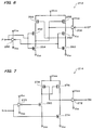
Fig. 7 schematically illustrates one example of the
structure of the second level shifter circuit 214 shown in Fig.
4.
-
A terminal N is electrically connected to the input
terminal of an inverter circuit 270 and the gate electrode of
an N-type transistor 274 whose source region is electrically
connected to the ground level and whose drain region is
electrically connected to the input terminal of an inverter
circuit 272. The inverter circuit 270 is supplied with the
power-supply level VDD and ground level VSS, and its output
corresponding to the logic level "H" is the potential
difference between both levels. The drain region of the N-type
transistor 274 is electrically connected to the drain region
of a P-type transistor 276 whose source region is electrically
connected to the power-supply level VDD2 and the gate electrode
of a P-type transistor 278. The gate electrode of the P-type
transistor 276, the drain region of the P-type transistor 278
and the drain region of an N-type transistor 280 are
electrically connected together. The output terminal of the
inverter circuit 270 is electrically connected to the gate
electrode of the N-type transistor 280 whose source region is
electrically connected to the ground level VSS. The output
terminal of the inverter circuit 272 is electrically connected
to a terminal ON.
-
As a signal with the logic level "H" whose signal level
is the power-supply level VDD is input from the terminal N, the
N-type transistor 274 is enabled, connecting the input terminal
of the inverter circuit 272 to the ground level VSS. The
inverter circuit 272 outputs the potential difference between
the power-supply level VDD2 and the ground level VSS from the
terminal ON as the logic level "H".
-
When a signal with the logic level "L" is input from the
terminal N, the signal level at the output terminal of the
inverter circuit 270 becomes the logic level "H" which is the
power-supply level VDD, thereby enabling the N-type transistor
280. The P-type transistor 276 is enabled so that the input
terminal of the inverter circuit 272 is connected to the
power-supply level VDD2. Therefore, the inverter circuit 272
outputs the logic level "L" from the terminal ON.
-
Fig. 8 schematically illustrates one example of the
structure of the output buffer circuit 220 shown in Fig. 4.
-
A terminal OP is electrically connected to the gate
electrode of a P-type transistor 290 whose source region is
electrically connected to the power-supply level VDD2. A
terminal ON is electrically connected to the gate electrode of
an N-type transistor 292 whose source region is electrically
connected to the ground level VSS. The drain region of the
P-type transistor 290 and the drain region of the N-type
transistor 292 are electrically connected together and are
further electrically connected to a terminal X, the drain
region of a P-type transistor 294 whose gate electrode and
source region are electrically connected to the power-supply
level VDD2 and the drain region of an N-type transistor 296 whose
gate electrode and source region are electrically connected to
the ground level VSS.
-
That is, in accordance with signals from the terminals
OP and ON, an output signal which operates on the potential
difference between the power-supply level VDD2 and the ground
level VSS is output from the terminal X. When a signal with
the logic level "L" is input from the terminal E shown in Fig.
4, therefore, the signals with the logic level "H" are input
from the terminals OP and ON as mentioned above. As a result,
the P-type transistor 290 and the N-type transistor 292 become
disabled, thus setting the terminal X in a high-impedance
state.
-
For example, I/O cells which include those circuits which
are comprised of transistors are placed on a semiconductor chip
as will be discussed below.
2.2 Lateral placement of I/O cells
-
In the following description, the placement of the I/O
cells which makes the longitudinal direction perpendicular to
the placement direction of the pads is called "lateral
placement".
-
Fig. 9 shows one example of the layout of I/O cells
arranged laterally in the semiconductor device according to the
embodiment.
-
Here, I/O cells 3201 to 3204 which are output cells shown
in Figs. 4 through 8 are placed in such a manner that the
longitudinal direction become perpendicular to the placement
direction of pads 3101 to 3104, in association with the pads
3101 to 3104 arranged along the outer peripheral portion of a
semiconductor chip 300 of the semiconductor device according
to the embodiment.
-
In Fig. 9, although the I/O cells 3201 to 3204 have similar
structures, the I/O cell 3201 indicates an internal signal line
that is formed by first-layer and second-layer interconnects
and the I/O cell 3202 indicates a transistor region where the
circuits that have been discussed in the foregoing description
referring to Figs. 4 to 8 are located.
-
Specifically, each I/O cell has a driver circuit portion
322 and an interface circuit portion 324 as indicated in the
I/O cell 3202. The output buffer circuit shown in Fig. 8 is
constructed in the driver circuit portion 322. The prebuffer
circuit portion shown in Fig. 6 and the first and second level
shifter circuits shown in Fig. 7 are constructed in the
interface circuit portion 324. The interface circuit portion
324 performs a function of interfacing with a core transistor
region 330.
-
The driver circuit portion 322 of each I/O cell has an
N-type transistor region 326 and a P-type transistor region 328,
in which a circuit of N-type transistors and a circuit of P-type
transistors are respectively formed.
-
In the driver circuit portion 322 and the interface
circuit portion 324, the internal power-supply level supply
line and ground-level supply line and signal lines of the
individual transistors are placed respectively by first- layer
interconnects 340 and 342.
-
Ground- level supply lines 350 and 352 for feeding the
ground level VSS to the N-type transistors or the like in the
N-type transistor region 326 are formed over the N-type
transistor region 326 of the driver circuit portion 322 by the
second-layer interconnect. That is, as the internal
interconnection of the driver circuit portion of an I/O cell
is realized by the first-layer interconnect, a layer overlying
the I/O cells laterally arranged along the outer peripheral
portion of the semiconductor chip can be arranged in a ring form
by the second-layer interconnect.
-
Likewise, power-supply level supply lines 360 and 362 for
feeding the power-supply levels VDD2 and VDD to the P-type
transistors or the like in the P-type transistor region 328 or
a ground-level supply line 364 for feeding the ground level VSS
are formed over the P-type transistor region 328 of the driver
circuit portion 322 by the second-layer interconnect. The
power-supply level supply lines 360 and 362 and ground-level
supply line 364 are likewise arranged in a ring form on a layer
overlying the I/O cells, laterally arranged along the outer
peripheral portion of the semiconductor chip, by the
second-layer interconnect.
-
Power-supply level supply lines 370 and 372 for feeding
the power-supply levels VDD2 and VDD to the P-type transistors
and N-type transistors, which constitute the prebuffer circuit
and the first and second level shifter circuits shown in Figs.
5 to 7, and ground- level supply lines 380 and 382 for feeding
the ground level VSS are formed over the interface circuit
portion 324 by the second-layer interconnect. The power-supply
level supply lines 370 and 372 and ground- level supply lines
380 and 382 are likewise arranged in a ring form on a layer
overlying the I/O cells, laterally arranged along the outer
peripheral portion of the semiconductor chip, by the
second-layer interconnect.
-
In this case, given that the length of the long side of
each I/O cell is A and the length of the short side is B, the
pads 3101 to 3104 can be placed with a pad pitch 390 which is
set to approximately B.
2.3 Vertically stacked placement of I/O cells
-
As mentioned earlier, as [A/B] or fewer columns of I/O
cells are placed in such a manner that, as shown in Fig. 2, the
longitudinal direction of the I/O cells become parallel to the
placement direction of the pads and plural levels of I/O cells
mentioned above are arranged from the outer peripheral portion
of the semiconductor chip toward the chip center portion, the
degree of freedom of designing the pad pitch can be improved.
Such a placement of I/O cells is hereinafter called "vertically
stacked placement".
-
Fig. 10 shows one example of the layout of I/O cells
arranged in a vertically stacked fashion in the semiconductor
device according to the embodiment.
-
Fig. 10 exemplifies the vertical 3-level stacked
placement on the assumption that [A/B] is "3". When "A" is
greater than "3B", therefore, the pad pitch can be increased
and the chip area can be reduced without changing the internal
core transistor region.
-
In this example, the I/O cells 3201 to 3206 which are
output cells shown in Figs. 4 through 8 are arranged in a
vertical 3-level stacked fashion in association with the pads
4101 to 4106 arranged along the outer peripheral portion of the
semiconductor chip 300 of the semiconductor device according
to the embodiment. Specifically, the I/O cells laterally
arranged as shown in Fig. 9 are stacked vertically with the
internal first and second interconnects intact, and
third-layer and fourth-layer interconnects are additionally
provided to connect to the first-layer or second-layer
interconnect that is placed in each I/O cell. The interface
circuit portions of the I/O cells placed in the vertical 3-level
stacked fashion are so arranged as to face the corresponding
interface circuit portions of the I/O cells in adjoining I/O
cell groups placed in the vertical 3-level stacked fashion.
-
The pads 4101, 4102, 4103, 4104, 4105 and 4106 are
electrically connected by a third-layer interconnect 420 in
association with 3203, 3201, 3202, 3206, 3204 and 3205.
-
The I/O cells 3201 to 3203 illustrate the connecting
relation between the internal first-layer and second-layer
interconnects and the individual pads. The I/O cells 3204 to
3206, on the other hand, illustrate the connecting relation
between the third-layer and fourth-layer interconnects,
omitting the first-layer and second-layer interconnects.
-
A ground-level supply line 430 and a power-supply level
supply line 432 for feeding the ground level VSS and the
power-supply level VDD are placed over those I/O cells by the
fourth-layer interconnect. As the interconnection of the I/O
cells is made by the first-layer and second-layer interconnects
and the interconnection between the I/O cells and the pads is
made by the third-line interconnect, a layer overlying the I/O
cells placed in the vertical 3-level stacked fashion along the
outer peripheral portion of the semiconductor chip can be
designed in a ring form by the fourth-layer interconnect.
-
A pad pitch 450 in this case is not limited to the width
B of the I/O cells, ensuring the pad placement more freely, and
the chip area can be made smaller than that in the case where
the height of the I/O cells is "A" because a height-directional
length 460 of the I/O cell placement region becomes "3B".
-
As the interface circuit portions in the individual I/O
cells in adjoining I/O cell groups are arranged to face one
another, the power-supply level supply lines for multiple power
supplies that are needed in, for example, the level shifter
circuits can be shared. This can significantly improve the
degree of freedom of the placement in the I/O cell placement
region and increase the width of the power supply lines as an
EMI countermeasure.
-
The invention is not limited to the embodiment but may
be modified in various other forms within the scope of the
invention.
-
Although it has been explained in the foregoing
description of the embodiment that the pads are arranged along
the outer peripheral portion of the semiconductor chip, the
embodiment is not limited to this particular type. For example,
the pads may be arranged in a zigzag form along the outer
peripheral portion of the semiconductor chip or the pads may
be placed in the active transistor region as in the case of
active surface bumps.
-
Although it has been explained in the foregoing
description of the embodiment that each I/O cell is of the
double power supply type to which first and second power-supply
levels are supplied and which comprises a driver circuit
portion and an interface circuit portion, the embodiment is not
limited to this particular type. The invention can also be
adapted to an I/O cell of the type to which three or more
power-supply levels are supplied and which comprises a
plurality of circuit portions correspond with those
power-supply levels.