EP1210755B1 - Integrated opto-electronic wavelength converter assembly - Google Patents
Integrated opto-electronic wavelength converter assembly Download PDFInfo
- Publication number
- EP1210755B1 EP1210755B1 EP00986182A EP00986182A EP1210755B1 EP 1210755 B1 EP1210755 B1 EP 1210755B1 EP 00986182 A EP00986182 A EP 00986182A EP 00986182 A EP00986182 A EP 00986182A EP 1210755 B1 EP1210755 B1 EP 1210755B1
- Authority
- EP
- European Patent Office
- Prior art keywords
- laser
- assembly
- photodetector
- electrical signal
- wavelength
- Prior art date
- Legal status (The legal status is an assumption and is not a legal conclusion. Google has not performed a legal analysis and makes no representation as to the accuracy of the status listed.)
- Expired - Lifetime
Links
Images


Classifications
-
- C—CHEMISTRY; METALLURGY
- C40—COMBINATORIAL TECHNOLOGY
- C40B—COMBINATORIAL CHEMISTRY; LIBRARIES, e.g. CHEMICAL LIBRARIES
- C40B30/00—Methods of screening libraries
- C40B30/04—Methods of screening libraries by measuring the ability to specifically bind a target molecule, e.g. antibody-antigen binding, receptor-ligand binding
-
- B—PERFORMING OPERATIONS; TRANSPORTING
- B82—NANOTECHNOLOGY
- B82Y—SPECIFIC USES OR APPLICATIONS OF NANOSTRUCTURES; MEASUREMENT OR ANALYSIS OF NANOSTRUCTURES; MANUFACTURE OR TREATMENT OF NANOSTRUCTURES
- B82Y20/00—Nanooptics, e.g. quantum optics or photonic crystals
-
- G—PHYSICS
- G01—MEASURING; TESTING
- G01N—INVESTIGATING OR ANALYSING MATERIALS BY DETERMINING THEIR CHEMICAL OR PHYSICAL PROPERTIES
- G01N33/00—Investigating or analysing materials by specific methods not covered by groups G01N1/00 - G01N31/00
- G01N33/48—Biological material, e.g. blood, urine; Haemocytometers
- G01N33/50—Chemical analysis of biological material, e.g. blood, urine; Testing involving biospecific ligand binding methods; Immunological testing
- G01N33/68—Chemical analysis of biological material, e.g. blood, urine; Testing involving biospecific ligand binding methods; Immunological testing involving proteins, peptides or amino acids
- G01N33/6803—General methods of protein analysis not limited to specific proteins or families of proteins
- G01N33/6845—Methods of identifying protein-protein interactions in protein mixtures
-
- G—PHYSICS
- G02—OPTICS
- G02F—OPTICAL DEVICES OR ARRANGEMENTS FOR THE CONTROL OF LIGHT BY MODIFICATION OF THE OPTICAL PROPERTIES OF THE MEDIA OF THE ELEMENTS INVOLVED THEREIN; NON-LINEAR OPTICS; FREQUENCY-CHANGING OF LIGHT; OPTICAL LOGIC ELEMENTS; OPTICAL ANALOGUE/DIGITAL CONVERTERS
- G02F1/00—Devices or arrangements for the control of the intensity, colour, phase, polarisation or direction of light arriving from an independent light source, e.g. switching, gating or modulating; Non-linear optics
- G02F1/01—Devices or arrangements for the control of the intensity, colour, phase, polarisation or direction of light arriving from an independent light source, e.g. switching, gating or modulating; Non-linear optics for the control of the intensity, phase, polarisation or colour
- G02F1/015—Devices or arrangements for the control of the intensity, colour, phase, polarisation or direction of light arriving from an independent light source, e.g. switching, gating or modulating; Non-linear optics for the control of the intensity, phase, polarisation or colour based on semiconductor elements with at least one potential jump barrier, e.g. PN, PIN junction
- G02F1/025—Devices or arrangements for the control of the intensity, colour, phase, polarisation or direction of light arriving from an independent light source, e.g. switching, gating or modulating; Non-linear optics for the control of the intensity, phase, polarisation or colour based on semiconductor elements with at least one potential jump barrier, e.g. PN, PIN junction in an optical waveguide structure
-
- H—ELECTRICITY
- H01—ELECTRIC ELEMENTS
- H01S—DEVICES USING THE PROCESS OF LIGHT AMPLIFICATION BY STIMULATED EMISSION OF RADIATION [LASER] TO AMPLIFY OR GENERATE LIGHT; DEVICES USING STIMULATED EMISSION OF ELECTROMAGNETIC RADIATION IN WAVE RANGES OTHER THAN OPTICAL
- H01S5/00—Semiconductor lasers
- H01S5/02—Structural details or components not essential to laser action
- H01S5/026—Monolithically integrated components, e.g. waveguides, monitoring photo-detectors, drivers
- H01S5/0262—Photo-diodes, e.g. transceiver devices, bidirectional devices
-
- H—ELECTRICITY
- H01—ELECTRIC ELEMENTS
- H01S—DEVICES USING THE PROCESS OF LIGHT AMPLIFICATION BY STIMULATED EMISSION OF RADIATION [LASER] TO AMPLIFY OR GENERATE LIGHT; DEVICES USING STIMULATED EMISSION OF ELECTROMAGNETIC RADIATION IN WAVE RANGES OTHER THAN OPTICAL
- H01S5/00—Semiconductor lasers
- H01S5/06—Arrangements for controlling the laser output parameters, e.g. by operating on the active medium
- H01S5/062—Arrangements for controlling the laser output parameters, e.g. by operating on the active medium by varying the potential of the electrodes
- H01S5/0625—Arrangements for controlling the laser output parameters, e.g. by operating on the active medium by varying the potential of the electrodes in multi-section lasers
- H01S5/06255—Controlling the frequency of the radiation
- H01S5/06256—Controlling the frequency of the radiation with DBR-structure
-
- H—ELECTRICITY
- H04—ELECTRIC COMMUNICATION TECHNIQUE
- H04B—TRANSMISSION
- H04B10/00—Transmission systems employing electromagnetic waves other than radio-waves, e.g. infrared, visible or ultraviolet light, or employing corpuscular radiation, e.g. quantum communication
- H04B10/29—Repeaters
- H04B10/291—Repeaters in which processing or amplification is carried out without conversion of the main signal from optical form
- H04B10/2912—Repeaters in which processing or amplification is carried out without conversion of the main signal from optical form characterised by the medium used for amplification or processing
- H04B10/2914—Repeaters in which processing or amplification is carried out without conversion of the main signal from optical form characterised by the medium used for amplification or processing using lumped semiconductor optical amplifiers [SOA]
-
- G—PHYSICS
- G01—MEASURING; TESTING
- G01N—INVESTIGATING OR ANALYSING MATERIALS BY DETERMINING THEIR CHEMICAL OR PHYSICAL PROPERTIES
- G01N2500/00—Screening for compounds of potential therapeutic value
- G01N2500/10—Screening for compounds of potential therapeutic value involving cells
-
- G—PHYSICS
- G02—OPTICS
- G02F—OPTICAL DEVICES OR ARRANGEMENTS FOR THE CONTROL OF LIGHT BY MODIFICATION OF THE OPTICAL PROPERTIES OF THE MEDIA OF THE ELEMENTS INVOLVED THEREIN; NON-LINEAR OPTICS; FREQUENCY-CHANGING OF LIGHT; OPTICAL LOGIC ELEMENTS; OPTICAL ANALOGUE/DIGITAL CONVERTERS
- G02F2201/00—Constructional arrangements not provided for in groups G02F1/00 - G02F7/00
- G02F2201/16—Constructional arrangements not provided for in groups G02F1/00 - G02F7/00 series; tandem
-
- H—ELECTRICITY
- H01—ELECTRIC ELEMENTS
- H01S—DEVICES USING THE PROCESS OF LIGHT AMPLIFICATION BY STIMULATED EMISSION OF RADIATION [LASER] TO AMPLIFY OR GENERATE LIGHT; DEVICES USING STIMULATED EMISSION OF ELECTROMAGNETIC RADIATION IN WAVE RANGES OTHER THAN OPTICAL
- H01S5/00—Semiconductor lasers
- H01S5/02—Structural details or components not essential to laser action
- H01S5/026—Monolithically integrated components, e.g. waveguides, monitoring photo-detectors, drivers
- H01S5/0265—Intensity modulators
-
- H—ELECTRICITY
- H01—ELECTRIC ELEMENTS
- H01S—DEVICES USING THE PROCESS OF LIGHT AMPLIFICATION BY STIMULATED EMISSION OF RADIATION [LASER] TO AMPLIFY OR GENERATE LIGHT; DEVICES USING STIMULATED EMISSION OF ELECTROMAGNETIC RADIATION IN WAVE RANGES OTHER THAN OPTICAL
- H01S5/00—Semiconductor lasers
- H01S5/04—Processes or apparatus for excitation, e.g. pumping, e.g. by electron beams
- H01S5/042—Electrical excitation ; Circuits therefor
- H01S5/0425—Electrodes, e.g. characterised by the structure
- H01S5/04256—Electrodes, e.g. characterised by the structure characterised by the configuration
-
- H—ELECTRICITY
- H01—ELECTRIC ELEMENTS
- H01S—DEVICES USING THE PROCESS OF LIGHT AMPLIFICATION BY STIMULATED EMISSION OF RADIATION [LASER] TO AMPLIFY OR GENERATE LIGHT; DEVICES USING STIMULATED EMISSION OF ELECTROMAGNETIC RADIATION IN WAVE RANGES OTHER THAN OPTICAL
- H01S5/00—Semiconductor lasers
- H01S5/04—Processes or apparatus for excitation, e.g. pumping, e.g. by electron beams
- H01S5/042—Electrical excitation ; Circuits therefor
- H01S5/0427—Electrical excitation ; Circuits therefor for applying modulation to the laser
-
- H—ELECTRICITY
- H01—ELECTRIC ELEMENTS
- H01S—DEVICES USING THE PROCESS OF LIGHT AMPLIFICATION BY STIMULATED EMISSION OF RADIATION [LASER] TO AMPLIFY OR GENERATE LIGHT; DEVICES USING STIMULATED EMISSION OF ELECTROMAGNETIC RADIATION IN WAVE RANGES OTHER THAN OPTICAL
- H01S5/00—Semiconductor lasers
- H01S5/06—Arrangements for controlling the laser output parameters, e.g. by operating on the active medium
- H01S5/062—Arrangements for controlling the laser output parameters, e.g. by operating on the active medium by varying the potential of the electrodes
- H01S5/0625—Arrangements for controlling the laser output parameters, e.g. by operating on the active medium by varying the potential of the electrodes in multi-section lasers
- H01S5/06251—Amplitude modulation
-
- H—ELECTRICITY
- H01—ELECTRIC ELEMENTS
- H01S—DEVICES USING THE PROCESS OF LIGHT AMPLIFICATION BY STIMULATED EMISSION OF RADIATION [LASER] TO AMPLIFY OR GENERATE LIGHT; DEVICES USING STIMULATED EMISSION OF ELECTROMAGNETIC RADIATION IN WAVE RANGES OTHER THAN OPTICAL
- H01S5/00—Semiconductor lasers
- H01S5/06—Arrangements for controlling the laser output parameters, e.g. by operating on the active medium
- H01S5/062—Arrangements for controlling the laser output parameters, e.g. by operating on the active medium by varying the potential of the electrodes
- H01S5/0625—Arrangements for controlling the laser output parameters, e.g. by operating on the active medium by varying the potential of the electrodes in multi-section lasers
- H01S5/06253—Pulse modulation
-
- H—ELECTRICITY
- H01—ELECTRIC ELEMENTS
- H01S—DEVICES USING THE PROCESS OF LIGHT AMPLIFICATION BY STIMULATED EMISSION OF RADIATION [LASER] TO AMPLIFY OR GENERATE LIGHT; DEVICES USING STIMULATED EMISSION OF ELECTROMAGNETIC RADIATION IN WAVE RANGES OTHER THAN OPTICAL
- H01S5/00—Semiconductor lasers
- H01S5/10—Construction or shape of the optical resonator, e.g. extended or external cavity, coupled cavities, bent-guide, varying width, thickness or composition of the active region
- H01S5/12—Construction or shape of the optical resonator, e.g. extended or external cavity, coupled cavities, bent-guide, varying width, thickness or composition of the active region the resonator having a periodic structure, e.g. in distributed feedback [DFB] lasers
- H01S5/1206—Construction or shape of the optical resonator, e.g. extended or external cavity, coupled cavities, bent-guide, varying width, thickness or composition of the active region the resonator having a periodic structure, e.g. in distributed feedback [DFB] lasers having a non constant or multiplicity of periods
- H01S5/1209—Sampled grating
-
- H—ELECTRICITY
- H01—ELECTRIC ELEMENTS
- H01S—DEVICES USING THE PROCESS OF LIGHT AMPLIFICATION BY STIMULATED EMISSION OF RADIATION [LASER] TO AMPLIFY OR GENERATE LIGHT; DEVICES USING STIMULATED EMISSION OF ELECTROMAGNETIC RADIATION IN WAVE RANGES OTHER THAN OPTICAL
- H01S5/00—Semiconductor lasers
- H01S5/10—Construction or shape of the optical resonator, e.g. extended or external cavity, coupled cavities, bent-guide, varying width, thickness or composition of the active region
- H01S5/12—Construction or shape of the optical resonator, e.g. extended or external cavity, coupled cavities, bent-guide, varying width, thickness or composition of the active region the resonator having a periodic structure, e.g. in distributed feedback [DFB] lasers
- H01S5/124—Construction or shape of the optical resonator, e.g. extended or external cavity, coupled cavities, bent-guide, varying width, thickness or composition of the active region the resonator having a periodic structure, e.g. in distributed feedback [DFB] lasers incorporating phase shifts
- H01S5/1243—Construction or shape of the optical resonator, e.g. extended or external cavity, coupled cavities, bent-guide, varying width, thickness or composition of the active region the resonator having a periodic structure, e.g. in distributed feedback [DFB] lasers incorporating phase shifts by other means than a jump in the grating period, e.g. bent waveguides
-
- H—ELECTRICITY
- H01—ELECTRIC ELEMENTS
- H01S—DEVICES USING THE PROCESS OF LIGHT AMPLIFICATION BY STIMULATED EMISSION OF RADIATION [LASER] TO AMPLIFY OR GENERATE LIGHT; DEVICES USING STIMULATED EMISSION OF ELECTROMAGNETIC RADIATION IN WAVE RANGES OTHER THAN OPTICAL
- H01S5/00—Semiconductor lasers
- H01S5/30—Structure or shape of the active region; Materials used for the active region
- H01S5/34—Structure or shape of the active region; Materials used for the active region comprising quantum well or superlattice structures, e.g. single quantum well [SQW] lasers, multiple quantum well [MQW] lasers or graded index separate confinement heterostructure [GRINSCH] lasers
- H01S5/3413—Structure or shape of the active region; Materials used for the active region comprising quantum well or superlattice structures, e.g. single quantum well [SQW] lasers, multiple quantum well [MQW] lasers or graded index separate confinement heterostructure [GRINSCH] lasers comprising partially disordered wells or barriers
- H01S5/3414—Structure or shape of the active region; Materials used for the active region comprising quantum well or superlattice structures, e.g. single quantum well [SQW] lasers, multiple quantum well [MQW] lasers or graded index separate confinement heterostructure [GRINSCH] lasers comprising partially disordered wells or barriers by vacancy induced interdiffusion
-
- H—ELECTRICITY
- H01—ELECTRIC ELEMENTS
- H01S—DEVICES USING THE PROCESS OF LIGHT AMPLIFICATION BY STIMULATED EMISSION OF RADIATION [LASER] TO AMPLIFY OR GENERATE LIGHT; DEVICES USING STIMULATED EMISSION OF ELECTROMAGNETIC RADIATION IN WAVE RANGES OTHER THAN OPTICAL
- H01S5/00—Semiconductor lasers
- H01S5/50—Amplifier structures not provided for in groups H01S5/02 - H01S5/30
- H01S5/5009—Amplifier structures not provided for in groups H01S5/02 - H01S5/30 the arrangement being polarisation-insensitive
- H01S5/5018—Amplifier structures not provided for in groups H01S5/02 - H01S5/30 the arrangement being polarisation-insensitive using two or more amplifiers or multiple passes through the same amplifier
Definitions
- This invention relates to wavelength converters of the type desirable in certain wavelength division multiplexed optical communication networks, as well as other applications where it is desirable to change the wavelength of the optical carrier of a modulated lightwave, and more particularly to optoelectronic wavelength converters in which an incoming lightwave having a first wavelength is detected by a photodetector that produces an electrical signal that in turn modulates a source of an outgoing lightwave having a desired second wavelength.
- Optoelectronic wavelength conversion processes have used as separate photodetectors, receiver and regeneration circuits, transmitter and driver circuits, and directly or externally modulated lasers.
- S.J.B. Yoo "Wavelength conversion technologies for WDM network applications," J. Lightwave Techn. 14 (6) (June, 1996).
- These discrete-component wavelength converters have tended to be relatively bulky and expensive to manufacture.
- the lasers generally have a fixed wavelength or a very limited tuning range.
- a monolithic wavelength converter assembly that provides for the process of detection and regeneration at some other wavelength.
- a monolithic wavelength converter assembly fabricated on one semiconductor substrate using compatible photonic integrated circuit technology for all components.
- a wavelength converter assembly where signal amplification is obtained without the use of electronic transistors.
- conditioning of the signal is done in combination with the detection or modulation process in the optical or electrical domain.
- a wavelength converter assembly that has a wide tuning range and all of the components are fabricated on one semiconductor substrate using compatible photonic integrated circuit technology.
- an object of the present invention is to provide an improved wavelength converter assembly.
- Another object of the present invention is to provide monolithic wavelength converter assembly that provides for the process of detection and regeneration at some other wavelength.
- a further object of the present invention is to provide a monolithic wavelength converter assembly fabricated on one semiconductor substrate using compatible photonic integrated circuit technology for all components.
- Yet another object of the present invention is to provide a wavelength converter assembly where signal amplification is obtained without the use of electronic transistors.
- Another object of the present invention is to provide a wavelength converter assembly where conditioning of the signal is done in combination with the detection or modulation process in the optical or electrical domain.
- a further object of the present invention is to provide a wavelength converter assembly that has a wide tuning range and all of the components are fabricated on one semiconductor substrate using compatible photonic integrated circuit technology.
- Yet a further object of the present invention is to provide a monolithic wavelength converter assembly that provides high data bandwidths.
- Another object of the present invention is to provide a monolithic wavelength converter assembly that provides a large output optical signal amplitude without the need for integrated transistors for electronic amplification.
- Still a further object of the present invention is to provide a monolithic wavelength converter assembly that provides conditioned output data waveforms with lower noise and distortion than at an input.
- Another object of the present invention is to provide a monolithic wavelength converter assembly that can be extended to large arrays of wavelength converters integrated on one substrate with photonic integrated circuit technology.
- An epitaxial structure is formed on a substrate with areas of different optical properties.
- a laser and a photodetector are formed in the epitaxial structure.
- the photodetector generates a first electrical signal in response to an optical signal.
- a conditioning circuit is coupled to the laser and the photodetector. The conditioning circuit receives the first electrical signal and provides a second electrical signal to the laser to modulate its optical output.
- a wavelength converter assembly in another embodiment, includes first and second semiconductor layers formed in an epitaxial structure. The first and second semiconductor layers having different dopings.
- a first waveguide layer is formed between the first and second semiconductor layers.
- the first waveguide layer includes first and second reflectors that define a resonant cavity.
- An optically active gain medium is disposed between the first and second reflectors.
- a photodetector is formed on the first semiconductor layer and includes an optically active absorber region. The photodetector generates a first electrical signal in response to an optical input.
- a wavelength converter assembly 10 of the present invention provides for the process of detection and regeneration at some other wavelength to be carried out with a monolithic apparatus.
- Wavelength converter assembly 10 is fabricated on one semiconductor substrate using compatible photonic integrated circuit (IC) technology for all components.
- IC photonic integrated circuit
- An advantage of wavelength converter assembly 10 over other devices is that signal amplification is obtained without the use of electronic transistors, which would involve incompatible fabrication technology.
- the conditioning of the signal may be done in combination with the detection or modulation process in the optical or electrical domain.
- Laser output from wavelength converter assembly 10 can have a wide tuning range so that a large number of output wavelengths are possible.
- the elements of wavelength converter assembly 10 are fabricated on a single wafer.
- the various elements are derived from a common epitaxial layer structure, and are fabricated by common process steps.
- Monolithic integration of optically dissimilar elements is accomplished by a method of fabrication that tailors optical properties of selected regions to a desired electro-optic function. Tailored optical properties, including the band gap, result in optically active and passive regions on the same wafer beginning from a common epitaxial layer structure. Further, the common fabrication process steps required for forming the apparatus elements are compatible with photonic device fabrication processes presently used in the lightwave industry. Thus, wavelength converter assembly 10 is readily manufacturable.
- the fabrication methods to selectively tailor the band gaps of regions of the wafer of wavelength converter assembly 10 include the steps of, implantation of impurities by low energy ions (less than about 200 eV) in a portion of a selected wafer region near the wafer surface; and annealing the wafer. This allows the impurities and vacancies implanted near the wafer surface to diffuse throughout the selected region and tailor the region's band gap to a desired electro-optic function.
- the effective bandgap should be somewhat larger (e.g., > 0.1 eV) than the operating lightwave energy, which is only slightly larger (typically ⁇ 0.01- 0.05 eV) than the effective bandgap of the active layers in the gain section.
- Integrated external modulator elements may have sections with the same larger bandgap as the other passive regions, or a bandgap intermediate between that of the active and passive sections for some desired functionality such as chirp reduction or improved -linearity.
- Integrated external amplifier elements M.J. O'Mahony, "Semiconductor laser Optical Amplifiers for Use in Future Fiber Systems, " J.
- the passive regions are created by selective removal of the lowest bandgap layers responsible for gain in the active regions within the same sequence as some other processing steps, such as grating formation in the mirror regions, are being carried out.
- the ion-implantation process is not necessary, but it may be utilized to better tailor other regions such as in integrated modulators and/or amplifier elements.
- This sequence is followed by a regrowth of the upper cladding layers required for the top portion of the optical waveguide.
- the data signal is available in electrical form for monitoring, tapping, and modification.
- a packet address or header information can be read and used to determine the routing of the information either by selection of the output wavelength or by setting the state of some switch that might follow the wavelength converter assembly.
- wavelength converter assembly 10 includes but are not limited to,: 1.) providing higher data bandwidths than currently available from currently available devices (T. Ido, S. Tanaka, M. Suzuki, M. Koizumi, H. Sano, and H. Inoue, "Ultra-High-Speed Multiple-Quantum-Well Electro-Absorption Optical Modulators with Integrated Waveguides," J. Lightwave Techn ., 14, (9), 2026-2034, (September 1996)), 2) providing a wider range of possible output wavelengths than currently available devices (V. Jayaraman, A. Mathur, L.A. Coldren and P.D. Dapkus, "Theory, Design, and Performance of Extended Tuning Range in Sampled Grating DBR Lasers," IEEE J.
- FIG. 1 illustrates certain generic elements, in block diagram form, of wavelength converter assembly 10. Illustrated are a multisection tunable laser element 12 (hereafter referred to as “laser 12"), a photodetector element 14 (hereafter referred to as “photodetector 14" and a current conditioning circuit element 16.
- laser 12 a multisection tunable laser element 12
- photodetector 14 a photodetector element 14
- current conditioning circuit element 16 The insets in the blocks are suggestive of the possible contents of elements 12, 14 and 16. Current from photodetector 14 modulates the laser 12 after being conditioned by the conditioning circuit.
- the net functionality provides wavelength conversion of an optical carrier modulated with some data such that: i) an arbitrary output wavelength within a band can be emitted; ii) the amplitude of the output can be adjusted within a useful range; and, iii) the noise and distortion on the data can be reduced.
- An important aspect of the invention is integration with a common photonic IC technology that has been described in F. Koyama and K. Iga, "Frequency Chirping in External Modulators," J . Lightwave Tech., 6 (1), 87-93, (January 1988); B. Mason, G.A. Fish, S.P. DenBaars, and L.A.
- elements 12, 14 and 16 provide an advantageous functionality that is not possible by interconnecting discrete elements using conventional printed circuit board or multi-chip module technology. Additionally, integration of elements 12, 14 and 16 enables low-cost, high-yield manufacturing processes to used.
- laser 12 can include first and second SGDBR's 18 and 20, a first and second SOA's 22 and 24 and EAM 26 and a multiple active region, MAR 28.
- Photodetector element 16 can include an SOA 30, first and second filters 32 and 34 and an absorber 36.
- Wavelength converter 10 offers a number of advantages.
- the surface-illuminated geometry photodetector 14 enables efficient and polarization independent coupling of light from optical fibers to absorber 36 of photodiode 12. Moreover, it does not require a large footprint on the substrate, and its modest dimensions, in one embodiment approximately 10- 30 ⁇ m in diameter, provide for high bandwidth, sensitive operation.
- the sensitivity of wavelength converter assembly 10 can be enhanced by incorporation of a multi-layer reflective stack beneath the wavelength converter assembly 10 to create a resonant-cavity photodiode 14. This stack forms the lower cladding region of laser 12 without any complication.
- surface-illuminated photodiode 14 is isolated by a proton and/or He+ ion implantation or other means well known to those skilled in the art, rendering the surrounding areas semi-insulating.
- the bottom contact of wavelength converter assembly 10 is brought out to the side for biasing and the top contact is directly interconnected to laser 12 with a shunt branch to conditioning circuit 16.
- a waveguide layer structure of photodetector 14 illustrated is Figure 2(b) is identical to the gain section of laser 12.
- the waveguide layer structure of photodetector 14 provides for higher saturation power than typical surface-illuminated designs.
- Optical coupling to the waveguide can be enhanced by the integration of compatible mode transformers using techniques such as those described in G.A. Fish, B. Mason, L.A. Coldren, and S.P. DenBaars, "Compact 1.55 ⁇ m Spot-Size Converters for Photonic Integrated Circuits," Integrated Photonics Research '99, Santa Barbara, CA, paper no. RWD4, 375-377, (July 19-21, 1999).
- a terminated traveling wave electrode structure may be incorporated.
- a suitable traveling wave electrode structure is described in 8. T. Ido, S. Tanaka, M. Suzuki, M. Koizumi, H. Sano, and H. Inoue, "Ultra-High-Speed Multiple-Quantum-Well Electro-Absorption Optical Modulators with Integrated Waveguides, "J. Lightwave Techn., 14, (9), 2026-2034, (September 1996).
- SOA 30 increases the optical signal incident on absorber section 36 and provides higher output photocurrent. This is advantageous by allowing the use of low-level data while still obtaining sufficient current to properly modulate laser 12 and also allows for data regeneration by a shunt conditioning circuit. SOA 30 can also provide for signal level adjustment in conjunction with an external control circuit. Noise added by SOA 30 may be removed by current conditioning circuit 18, resulting in a noise figure that does not degrade the data.
- the layer structure of SOA 30 can be identical to the gain section of laser 12.
- photodetector 14 is integrated with SOA 30 and a tunable resonant-cavity filter.
- This waveguide geometry reflects light signals that are not within the resonant bandwidth of the resonant cavity formed by two DBR's 38 and 40 and enhances the signal.
- a shorter absorber length may be used for total absorption and high quantum efficiency. This shortened length, in turn, reduces photodetector's 14 capacitance, enabling very high bandwidth operation.
- Figures 3(a) and 3(b) are cross-sectional views of the semiconductor layer waveguide structure of the Figure 2(d) photodetector 14.
- passive sections are created by removal of the active regions prior to regrowth.
- passive sections are created by variable thickness and composition quantum-wells via intermixing after uniform growth or selective area growth.
- Figure 3(a) and 3(b) illustrate that waveguide photodetectors 14 are compatible with the tunable sections of laser 12 that are illustrated in Figure 5. It will be appreciated that various sections shown in Figures 3(a) and 3(b) are omitted in the Figure 2(a), 2(b) and 2(c) embodiments.
- FIGS 4(a) and 5(a) illustrate embodiments of wavelength converter assembly 10 with a series-connected, axially segmented active region that obtains signal gain within a widely tunable SGDBR laser 12 as described in United States Patent 4,896,325.
- the principle of operation of each SGDBR 18 and 20 is well known to those skilled in the art, as is the concept of using MAR 28 within a single optical cavity to obtain a differential efficiency greater than unity.
- Figures 4(b) and 5(b) illustrate another embodiment employing the same concepts.
- the separate pin active regions of the gain section are integrated vertically with the series electrical connections derived from intermediate n + - p + tunnel diodes.
- This layer structure is particularly useful in combination with the vertical resonant-cavity photodiode embodiment of Figure 2(a), since more absorption can lead to photodiodes with broader optical bandwidth and better efficiency as well.
- Absorbers can be placed at standing wave peaks and the tunnel diodes at standing wave nulls to provide a multiplication in absorbency by nearly 2x the number of active regions.
- Figure 4(c) illustrates another embodiment of the invention.
- the signal gain is enhanced relative to other embodiments by the addition of integrated SOA 22 external to the laser cavity.
- the data signal current is still applied to the gain section, and the gain section may either be of a conventional single active region, or MAR 28, as in Figure 4(a) or 4(b) embodiments, for more signal gain.
- External SOA 22 can provide about 20 dB of gain, whereas the multiple active region design provides for roughly unity gain.
- Normal lasers have differential efficiencies ⁇ 20 - 30 %; thus the MAR 28 design gives about 3 to 5x enhancement.
- the MAR 28 design is advantageous because it does not degrade the signal-to-noise ratio, whereas SOA 22 does.
- the constant noise added by SOA 22 can be negligible.
- This geometry also allows for the leveling of the output data signal level via an external control circuit.
- SOA's 22 and 24 may also be advantageously employed to increase the input carrier level and output modulated data.
- Use of MAR 28 actives may also be advantageous if laser RIN is to be minimized. Since the active region can be biased by a high-impedance source in this case, no low-source-impedance high-frequency signal, the inherent noise on laser 12 output can be reduced to sub-shot noise levels.
- SOA's 22 and 24 at laser's 12 output can be avoided by accomplishing the desired signal gain in photodetector 14 where their noise may be removed by the current conditioning circuit. This provides for signal gain, with a maximal signal-to-noise ratio.
- the current conditioning circuit 16 can be easily created in Si-CMOS if external shunting circuits are used.
- the packaging may not provide sufficiently low shunt capacitance, so at least some of the functionality may be desirable to have on-chip.
- the shunt impedance of this circuit is shown in Figure 7. With this circuit shunting the drive current, noise on the baseline (logical '0') and maximum (logical '1') of the data can be removed, provided that the signal level can be adjusted to the appropriate levels by the gain components in photodetector 14.
- Diode chains can be used to threshold and limit the level of the modulating data signal. These can be integrated using the same fabrication steps already necessary to create photodetector 14 and tunable elements of laser 12 shown in Figures 2 through 5.
- conditioning circuits are possible that provide the characteristic of Figure 7 and the desired laser active region (gain) or EAM bias using compatible integrable technology, and these can be obtained by using standard circuit design packages. If the photocurrent is to be applied to the EAM, such as may be desired for high-speed operation, then current conditioning circuit 16 may supply the correct reverse bias voltage to the EAM for some desired operation. Such desired operations include but are not limited to minimizing the chirp or maximizing the linearity for an output wavelength from laser 12.
- Wavelength converter assembly 10 is a monolithically integrated optoelectronic wavelength converter assembly. Particular embodiments comprise: photodetector 14 electrically coupled to a multi-section, laser 12 having a differential efficiency greater than unity, where the photocurrent can be conditioned by a circuit element to provide tapping, thresholding, and limiting of the detected data. Key elements of circuit conditioning circuit 16 can be integrable with the same fabrication steps required for photodetector 14 and laser 12.
- photodetector 14 is an edge-illuminated waveguide photodetector. In other embodiments, photodetector 14 is a surface-illuminated element.
- SOA 30 may be integrated with photodetector 14 using the same fabrication sequence for additional gain or level control.
- tunable waveguide filter 42 may also be incorporated with the same fabrication sequence to filter out unwanted signals or noise from SOA 30.
- Laser 12 can use SGDBR's 18 and 20 and gain and phase-shift sections to provide for output wavelength tunability over a range of several tens of nanometers.
- the gain section of laser 12 may contain several active regions that are driven electrically in series, and/or laser 12 may incorporate an integrated external SOA at its output port.
- the conditioned photocurrent is connected to an integrated external modulator to provide reduced wavelength chirping and generally enable higher data rate operation than feasible with direct modulation of the gain section of laser 12.
- Electro-absorption modulators EAMs
- Robert G. Walker "High-Speed III-V Semiconductor Intensity Modulators," IEEE J. Quant. Electron., 27, (3), 654-667, (March 1991); F. Koyama and K. Iga, "Frequency Chirping in External Modulators," J. Lightwave Tech., 6 (1), 87-93, (January 1988); B. Mason, G.A. Fish, S.P. DenBaars, and L.A.
- current conditioning circuit element 16 is nonlinear and consists of a connection to an external source to supply laser 12 with a necessary threshold current.
- current conditioning circuit 16 includes a microwave filter to remove subcarrier header information.
- current conditioning circuit 16 can comprise a limiting circuit to shunt off any currents above a given level.
- Current conditioning circuit element 16 can also comprise a thresholding circuit to shunt away photocurrent below a given level. These latter circuits may be partially external to the monolithic photonic IC, or they may comprise appropriate series diode chains that can be compatibly integrated.
- wavelength converter assembly 10 can be created with a standardized photonic IC fabrication processes. Thus, various options can be added dependant only upon the desired specifications and without the need to develop a new or incompatible materials growth and device fabrication sequence.
- wavelength converter assembly 10 includes elements that are based on InP substrates, which can provide wavelength conversion and other functionality near the 1.55 ⁇ m wavelength band. It will be appreciated that wavelength converter assembly 10 can use other material platforms.
- wavelength converter assembly 10 is illustrated in Figures 8(a) and (b).
- metal interconnects between photodetector 14 and laser12 are avoided by integrating photodetector 14 directly on top of laser12. This eliminates any excess series resistance or inductance or shunt capacitance between the input and output stages and optimizes the configuration for high-data rate operation.
- Semi-insulating regrowth of a buried-heterostructure waveguide is also illustrated for high-speed operation.
- Current conditioning circuit 16 can also be connected by contacting to the intermediate p-InGaAsP layer between vertically stacked photodetector 14 and laser 12. As illustrated, the connection is directly to the integrated modulator, which can be the preferred connection for high-speed low-chirp operation.
- Vertical illumination is also illustrated, but a horizontal waveguide detector configuration is also possible.
- the vertical configuration may be preferred since there is less crosstalk between input and output lightwave signals.
- Such vertical integration is obtained by performing several regrowth steps as is common in such photonic integrated circuits using techniques well known to those skilled in the art.
- a reverse bias voltage is applied between bias-1 and bias-2 electrodes to deplete the InGaAs absorber region and provide minimal sweep out times for photocarriers.
- Bias-2 would is set to the voltage appropriate for optimal operation of the modulator.
- Example dc potentials include but are not limited to, - 2 V on bias-2 electrode and - 6 V on bias-1 electrode.
- the thickness of the InGaAs absorber is adjusted to be sufficient to absorb most of the incoming light but not so thick as to slow the transit of carriers to the contact layers. It will be appreciated that an avalanche photodetector (APD) may also be used in place of the simple pin detector indicated in Figures 8(a) and (b). In this case additional layers are desired to optimize the gain-bandwidth product of the APD.
- APD avalanche photodetector
Abstract
Description
- This invention relates to wavelength converters of the type desirable in certain wavelength division multiplexed optical communication networks, as well as other applications where it is desirable to change the wavelength of the optical carrier of a modulated lightwave, and more particularly to optoelectronic wavelength converters in which an incoming lightwave having a first wavelength is detected by a photodetector that produces an electrical signal that in turn modulates a source of an outgoing lightwave having a desired second wavelength.
- Optoelectronic wavelength conversion processes have used as separate photodetectors, receiver and regeneration circuits, transmitter and driver circuits, and directly or externally modulated lasers. S.J.B. Yoo, "Wavelength conversion technologies for WDM network applications," J. Lightwave Techn. 14 (6) (June, 1996). These discrete-component wavelength converters have tended to be relatively bulky and expensive to manufacture. Also, the lasers generally have a fixed wavelength or a very limited tuning range.
- There is a need for a monolithic wavelength converter assembly that provides for the process of detection and regeneration at some other wavelength. There is a need for a monolithic wavelength converter assembly fabricated on one semiconductor substrate using compatible photonic integrated circuit technology for all components. There is a further need for a wavelength converter assembly where signal amplification is obtained without the use of electronic transistors. There is yet a further need for a wavelength converter assembly where conditioning of the signal is done in combination with the detection or modulation process in the optical or electrical domain. There is still a further need for a wavelength converter assembly that has a wide tuning range and all of the components are fabricated on one semiconductor substrate using compatible photonic integrated circuit technology.
- Bar-Chaim N et al: "Monolithic Optoelectronic Integration of a GaAlAs Laser, a Field Effect Transistor and a Photodiode" Applied Physics Letters, US, American Institute of Physics. New York, vol. 44, no. 10, 15 May 1984 (1984-05-15), pages 941-943, describes a low threshold buried heterostructure laser, a metal-semiconductor field effect transistor, and a p-i-n photodiode integrated on to a semi-insulating GaAs substrate. The circuit operated as a rudimentary optical repeater with a gain-bandwidth product of 178MHz.
- US-A-5 742 045 (Kimmet James S et al) 21 April 1998 (1998-04-21), describes an apparatus that uses diode laser logic to from a configurable optical gate system, comprising a laser diode and a photodetector integrated in the same epitaxial structure and electrically interconnected.
- US-A-5 625 636 (Jewell Jack L et al) 29 April 1997 (1997-04-29), describes integration of photoactive and electroactive components with vertical cavity surface emitting lasers.
- US-A-5 674 778 (Lee Kwyro et al) 7 October 1997 (1997-10-07), describes a method of manufacturing an optoelectronic circuit including a heterojunction bipolar transistor, laser and photodetector.
- Byoung-Sung Kim et al; "Dynamic analyis of widely tunable laser diodes integrated with sampled- and chirped-grating distributed Bragg reflectors and an electroabsorption modulator IEICE Transactions on Electronics, Aug. 1998, Inst. Electron. Inf. & Comun. Eng. Japan, vol. E81-C, no. 8, pages 1342-1349, describes dynamic analysis of wide tunable laser diodes integrated with sampled- and chirped-grating distributed Bragg reflectors and an electroabsorption modulator.
-
- Figure 1 is a block diagram of one embodiment of a wavelength converter assembly of the present invention.
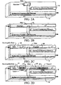
- Figure 2(a) is a top down schematic view of a waveguide photodetector that can be part of the Figure 1 wavelength converter assembly.
- Figure 2(b) is a top down schematic view of a waveguide photodetector that can be part of the Figure 1 wavelength converter assembly.
- Figure 2(c) is a top down schematic view of waveguide photodetector integrated with a semiconductor-optical amplifier ("SOA") preamplifier that can be part of the Figure 1 wavelength converter assembly.
- Figure 2(d) is a top down schematic view of a waveguide photodetector integrated with a SOA preamplifier and a tunable resonant-cavity filter that can be part of the Figure 1 wavelength converter assembly.
- Figure 3(a) is a cross sectional view of the semiconductor layer structure of the Figure 2(d) assembly in which passive sections are created by removal of the active regions prior to regrowth.
- Figure 3(b) is a cross sectional view of the semiconductor layer structure of the Figure 2(d) assembly in which passive sections are created by variable thickness and composition quantum-wells via intermixing after uniform growth or selective area growth.
- Figure 4(a) is a schematic top down view of a sampled-grating distributed-Bragg-reflector ("SGDBR") tunable laser having a series-connected, axially segmented multiple-active region that can be part of the Figure 1 wavelength converter assembly.
- Figure 4(b) is a schematic of a SGDBR tunable laser that has a series-connected, vertically stacked multiple-active region that can be part of the Figure 1 wavelength converter assembly.
- Figure 4(c) is a schematic top down view of a SGDBR tunable laser with an integrated external SOA that can be part of the Figure 1 wavelength converter assembly.
- Figure 4(d) is a schematic top down view of a SGDBR tunable laser with an integrated external electro-absorption modulator (EAM) and two SOAs that can be part of the Figure 1 wavelength converter assembly..
- Figure 5(a) is a cross sectional view of the Figure 4(a) structure.
- Figure 5(b) is a cross sectional view of the Figure 4(b) structure.
- Figure 6 is schematic diagram of an equivalent circuit that can be used with the structures of Figures 2(a), 2(b), 4(a) and 4(b) as well as an integrable current conditioning circuit.
- Figure 7 is a plot of the desired impedance of the Figure 1 nonlinear current conditioning circuit.
- Figures 8(a) and (b) illustrate an embodiment of a monolithic wavelength converter assembly of the present invention where the photodetector is integrated directly on top of the laser.
- Accordingly, an object of the present invention is to provide an improved wavelength converter assembly.
- Another object of the present invention is to provide monolithic wavelength converter assembly that provides for the process of detection and regeneration at some other wavelength.
- A further object of the present invention is to provide a monolithic wavelength converter assembly fabricated on one semiconductor substrate using compatible photonic integrated circuit technology for all components.
- Yet another object of the present invention is to provide a wavelength converter assembly where signal amplification is obtained without the use of electronic transistors.
- Another object of the present invention is to provide a wavelength converter assembly where conditioning of the signal is done in combination with the detection or modulation process in the optical or electrical domain.
- A further object of the present invention is to provide a wavelength converter assembly that has a wide tuning range and all of the components are fabricated on one semiconductor substrate using compatible photonic integrated circuit technology.
- Yet a further object of the present invention is to provide a monolithic wavelength converter assembly that provides high data bandwidths.
- Another object of the present invention is to provide a monolithic wavelength converter assembly that provides a large output optical signal amplitude without the need for integrated transistors for electronic amplification.
- Still a further object of the present invention is to provide a monolithic wavelength converter assembly that provides conditioned output data waveforms with lower noise and distortion than at an input.
- Another object of the present invention is to provide a monolithic wavelength converter assembly that can be extended to large arrays of wavelength converters integrated on one substrate with photonic integrated circuit technology.
- These and other objects of the present invention are achieved in a wavelength converter assembly as defined in
claim 1 and are achieved by a method as defined in claim 33. An epitaxial structure is formed on a substrate with areas of different optical properties. A laser and a photodetector are formed in the epitaxial structure. The photodetector generates a first electrical signal in response to an optical signal. A conditioning circuit is coupled to the laser and the photodetector. The conditioning circuit receives the first electrical signal and provides a second electrical signal to the laser to modulate its optical output. - In another embodiment of the present invention, a wavelength converter assembly includes first and second semiconductor layers formed in an epitaxial structure. The first and second semiconductor layers having different dopings. A first waveguide layer is formed between the first and second semiconductor layers. The first waveguide layer includes first and second reflectors that define a resonant cavity. An optically active gain medium is disposed between the first and second reflectors. A photodetector is formed on the first semiconductor layer and includes an optically active absorber region. The photodetector generates a first electrical signal in response to an optical input.
- Referring now to Figure 1, a
wavelength converter assembly 10 of the present invention provides for the process of detection and regeneration at some other wavelength to be carried out with a monolithic apparatus.Wavelength converter assembly 10 is fabricated on one semiconductor substrate using compatible photonic integrated circuit (IC) technology for all components. An advantage ofwavelength converter assembly 10 over other devices is that signal amplification is obtained without the use of electronic transistors, which would involve incompatible fabrication technology. Moreover, the conditioning of the signal may be done in combination with the detection or modulation process in the optical or electrical domain. Laser output fromwavelength converter assembly 10 can have a wide tuning range so that a large number of output wavelengths are possible. - In one embodiment, the elements of
wavelength converter assembly 10 are fabricated on a single wafer. The various elements are derived from a common epitaxial layer structure, and are fabricated by common process steps. - Monolithic integration of optically dissimilar elements is accomplished by a method of fabrication that tailors optical properties of selected regions to a desired electro-optic function. Tailored optical properties, including the band gap, result in optically active and passive regions on the same wafer beginning from a common epitaxial layer structure. Further, the common fabrication process steps required for forming the apparatus elements are compatible with photonic device fabrication processes presently used in the lightwave industry. Thus,
wavelength converter assembly 10 is readily manufacturable. - In a particular embodiment, the fabrication methods to selectively tailor the band gaps of regions of the wafer of
wavelength converter assembly 10 include the steps of, implantation of impurities by low energy ions (less than about 200 eV) in a portion of a selected wafer region near the wafer surface; and annealing the wafer. This allows the impurities and vacancies implanted near the wafer surface to diffuse throughout the selected region and tailor the region's band gap to a desired electro-optic function. - For example, in the passive waveguide regions of the phase shift and mirror sections of a
tunable laser element 12, the effective bandgap should be somewhat larger (e.g., > 0.1 eV) than the operating lightwave energy, which is only slightly larger (typically ~ 0.01- 0.05 eV) than the effective bandgap of the active layers in the gain section. Integrated external modulator elements may have sections with the same larger bandgap as the other passive regions, or a bandgap intermediate between that of the active and passive sections for some desired functionality such as chirp reduction or improved -linearity. Integrated external amplifier elements (M.J. O'Mahony, "Semiconductor laser Optical Amplifiers for Use in Future Fiber Systems, "J. Lightwave Techn. 6 (4) (April, 1988.); A. E. Kelly, I. F. Lealman, L. J. Rivers, S. D. Perrin, and M. Silver, "Low noise figure (7.2 dB) and high gain (29dB) semiconductor optical amplifier with a single layer AR coating," Electron. Lett., 33 pp 536-8 (1997.)) may have the same bandgap as the active gain section or a slightly modified bandgap for some functionality, such as increased saturation power or improved chirp of modulator/amplifier combinations. Robert G. Walker, "High-Speed III-V Semiconductor Intensity Modulators," IEEE J. Quant. Electron., 27, (3), 654-667, (March 1991); F. Koyama and K. Iga, "Frequency Chirping in External Modulators," J. Lightwave Tech., 6 (1), 87-93, (January 1938). - In various embodiments of the present invention, the passive regions are created by selective removal of the lowest bandgap layers responsible for gain in the active regions within the same sequence as some other processing steps, such as grating formation in the mirror regions, are being carried out. B. Mason, G.A. Fish, S.P. DenBaars, and L.A. Coldren, "Widely Tunable Sampled Grating DBR Laser with Integrated Electroabsorption Modulator," Photon. Tech. Letts., 11, (6), 638-640, (June 1999). In such cases the ion-implantation process is not necessary, but it may be utilized to better tailor other regions such as in integrated modulators and/or amplifier elements. This sequence is followed by a regrowth of the upper cladding layers required for the top portion of the optical waveguide.
- According to aspects of the present invention, the data signal is available in electrical form for monitoring, tapping, and modification. In particular, a packet address or header information can be read and used to determine the routing of the information either by selection of the output wavelength or by setting the state of some switch that might follow the wavelength converter assembly. These and other desirable features are all incorporated within novel, monolithically-integrated optoelectronic wavelength converter assembly structures that make use of a manufacturable, integrated photonic IC technology. G.A. Fish, B. Mason, L.A. Coldren, and S.P. DenBaars, "Compact 1.55µm Spot-Size Converters for Photonic Integrated Circuits," Integrated Photonics Research '99, Santa Barbara, CA, paper no. RWD4, 375-377, (July 19-21, 1999).
- Further features of
wavelength converter assembly 10 include but are not limited to,: 1.) providing higher data bandwidths than currently available from currently available devices (T. Ido, S. Tanaka, M. Suzuki, M. Koizumi, H. Sano, and H. Inoue, "Ultra-High-Speed Multiple-Quantum-Well Electro-Absorption Optical Modulators with Integrated Waveguides," J. Lightwave Techn., 14, (9), 2026-2034, (September 1996)), 2) providing a wider range of possible output wavelengths than currently available devices (V. Jayaraman, A. Mathur, L.A. Coldren and P.D. Dapkus, "Theory, Design, and Performance of Extended Tuning Range in Sampled Grating DBR Lasers," IEEE J. Quantum Elec., 29, (6), 1824-1834, (June 1993)), 3.) providing equal or larger output optical signal amplitude than current devices without the need for integrated transistors for electronic amplification (J.K. Kim, E. Hall, O. Sjölund, and L.A. Coldren, "Epitaxially-Stacked Multiple-Active-Region 1.55 µm Lasers for Increased Differential Efficiency," Appl. Phys. Letts., 74, (22) 3251-3253, (May 31, 1999); J.T. Getty, O. Buchinsky, R.A. Slavatore, B. Mason, P.G. Piva, S. Charbonneau, K.S. Grabowski, and L.A. Coldren, "Monolithic Series-Connected 1.55µm Segmented-Ridge Lasers," Electronics Letters, 35, (15), 1257-1258, (July 22, 1999)), 4.) providing conditioned output data waveforms having lower noise and distortion than at the input and 5.) providing capabilities for extensions to large arrays of such wavelength converters, the arrays integrated on one substrate with existing photonic IC technology. Coldren, L., "Diode Lasers and Photonic Integrated Circuits," Wiley, (1995). - Figure 1 illustrates certain generic elements, in block diagram form, of
wavelength converter assembly 10. Illustrated are a multisection tunable laser element 12 (hereafter referred to as "laser 12"), a photodetector element 14 (hereafter referred to as "photodetector 14" and a currentconditioning circuit element 16. The insets in the blocks are suggestive of the possible contents ofelements photodetector 14 modulates thelaser 12 after being conditioned by the conditioning circuit. The net functionality provides wavelength conversion of an optical carrier modulated with some data such that: i) an arbitrary output wavelength within a band can be emitted; ii) the amplitude of the output can be adjusted within a useful range; and, iii) the noise and distortion on the data can be reduced. An important aspect of the invention is integration with a common photonic IC technology that has been described in F. Koyama and K. Iga, "Frequency Chirping in External Modulators," J. Lightwave Tech., 6 (1), 87-93, (January 1988); B. Mason, G.A. Fish, S.P. DenBaars, and L.A. Coldren, "Widely Tunable Sampled Grating DBR Laser with Integrated Electroabsorption Modulator," Photon. Tech. Letts., 11, (6), 638-640, (June 1999). Moreover, integration ofelements elements - As illustrated in Figure 1,
laser 12 can include first and second SGDBR's 18 and 20, a first and second SOA's 22 and 24 andEAM 26 and a multiple active region,MAR 28.Photodetector element 16 can include anSOA 30, first andsecond filters absorber 36. -
Wavelength converter 10 offers a number of advantages. In the embodiment illustrated in Figure 2(a), the surface-illuminatedgeometry photodetector 14 enables efficient and polarization independent coupling of light from optical fibers toabsorber 36 ofphotodiode 12. Moreover, it does not require a large footprint on the substrate, and its modest dimensions, in one embodiment approximately 10- 30 µm in diameter, provide for high bandwidth, sensitive operation. In various embodiments, the sensitivity ofwavelength converter assembly 10 can be enhanced by incorporation of a multi-layer reflective stack beneath thewavelength converter assembly 10 to create a resonant-cavity photodiode 14. This stack forms the lower cladding region oflaser 12 without any complication. As in other embodiments, surface-illuminatedphotodiode 14 is isolated by a proton and/or He+ ion implantation or other means well known to those skilled in the art, rendering the surrounding areas semi-insulating. In particular embodiments, the bottom contact ofwavelength converter assembly 10 is brought out to the side for biasing and the top contact is directly interconnected tolaser 12 with a shunt branch toconditioning circuit 16. - A waveguide layer structure of
photodetector 14 illustrated is Figure 2(b) is identical to the gain section oflaser 12. In this embodiment, the waveguide layer structure ofphotodetector 14 provides for higher saturation power than typical surface-illuminated designs. Optical coupling to the waveguide can be enhanced by the integration of compatible mode transformers using techniques such as those described in G.A. Fish, B. Mason, L.A. Coldren, and S.P. DenBaars, "Compact 1.55µm Spot-Size Converters for Photonic Integrated Circuits," Integrated Photonics Research '99, Santa Barbara, CA, paper no. RWD4, 375-377, (July 19-21, 1999). For ultra high bandwidth embodiments, such as for example greater than 50 GHz, a terminated traveling wave electrode structure may be incorporated. A suitable traveling wave electrode structure is described in 8. T. Ido, S. Tanaka, M. Suzuki, M. Koizumi, H. Sano, and H. Inoue, "Ultra-High-Speed Multiple-Quantum-Well Electro-Absorption Optical Modulators with Integrated Waveguides, "J. Lightwave Techn., 14, (9), 2026-2034, (September 1996). - Referring now to Figure 2(c), the addition of an optical preamplifier,
SOA 30, increases the optical signal incident onabsorber section 36 and provides higher output photocurrent. This is advantageous by allowing the use of low-level data while still obtaining sufficient current to properly modulatelaser 12 and also allows for data regeneration by a shunt conditioning circuit.SOA 30 can also provide for signal level adjustment in conjunction with an external control circuit. Noise added bySOA 30 may be removed bycurrent conditioning circuit 18, resulting in a noise figure that does not degrade the data. The layer structure ofSOA 30 can be identical to the gain section oflaser 12. - If the signal to noise level is low, or if unwanted data at another wavelength is present in the input lightwave, or if a shorter absorber section is desired, it may be advantageous to place
absorber 36 within a resonant cavity to filter out unwanted signals out-of-band. As illustrated in Figure 2(d),photodetector 14 is integrated withSOA 30 and a tunable resonant-cavity filter. This waveguide geometry reflects light signals that are not within the resonant bandwidth of the resonant cavity formed by two DBR's 38 and 40 and enhances the signal. A shorter absorber length may be used for total absorption and high quantum efficiency. This shortened length, in turn, reduces photodetector's 14 capacitance, enabling very high bandwidth operation. - Figures 3(a) and 3(b) are cross-sectional views of the semiconductor layer waveguide structure of the Figure 2(d)
photodetector 14. In Figure 3(a) passive sections are created by removal of the active regions prior to regrowth. In Figure 3(b) passive sections are created by variable thickness and composition quantum-wells via intermixing after uniform growth or selective area growth. Figure 3(a) and 3(b) illustrate thatwaveguide photodetectors 14 are compatible with the tunable sections oflaser 12 that are illustrated in Figure 5. It will be appreciated that various sections shown in Figures 3(a) and 3(b) are omitted in the Figure 2(a), 2(b) and 2(c) embodiments. - Figures 4(a) and 5(a) illustrate embodiments of
wavelength converter assembly 10 with a series-connected, axially segmented active region that obtains signal gain within a widelytunable SGDBR laser 12 as described in United States Patent 4,896,325. The principle of operation of eachSGDBR MAR 28 within a single optical cavity to obtain a differential efficiency greater than unity. - Figures 4(b) and 5(b) illustrate another embodiment employing the same concepts. In this embodiment, the separate pin active regions of the gain section are integrated vertically with the series electrical connections derived from intermediate n +-p + tunnel diodes. This layer structure is particularly useful in combination with the vertical resonant-cavity photodiode embodiment of Figure 2(a), since more absorption can lead to photodiodes with broader optical bandwidth and better efficiency as well. Absorbers can be placed at standing wave peaks and the tunnel diodes at standing wave nulls to provide a multiplication in absorbency by nearly 2x the number of active regions.
- Figure 4(c) illustrates another embodiment of the invention. In Figure 4(c), the signal gain is enhanced relative to other embodiments by the addition of
integrated SOA 22 external to the laser cavity. The data signal current is still applied to the gain section, and the gain section may either be of a conventional single active region, orMAR 28, as in Figure 4(a) or 4(b) embodiments, for more signal gain.External SOA 22 can provide about 20 dB of gain, whereas the multiple active region design provides for roughly unity gain. Normal lasers have differential efficiencies ~ 20 - 30 %; thus theMAR 28 design gives about 3 to 5x enhancement. TheMAR 28 design is advantageous because it does not degrade the signal-to-noise ratio, whereasSOA 22 does. However, if the signal level is already high, as it can be with a MAR gain section and/or gain inphotodetector 14, the constant noise added bySOA 22 can be negligible. This geometry also allows for the leveling of the output data signal level via an external control circuit. - If the signal bandwidth is very high, such as but not limited to 15GHz or greater, direct modulation of
laser 12 may be difficult. Also, if chirping of the wavelength is a problem, direct modulation may not be an optimal solution. Finally, if the output wavelength oflaser 12 must be set very accurately, direct modulation may compromise the ability ofcontrol circuit 16 to hold the wavelength with sufficient accuracy. For all of these reasons, use of external modulation, such as illustrated in Figure 4(d), may be desired. In this case, the data signal current is applied to the integrated external modulator. An EAM 44 is shown, but an interferometric modulator, such as a Mach-Zehender or directional coupler modulator or other equivalent, is also possible by using passive waveguide sections of appropriate design. As indicated, SOA's 22 and 24 may also be advantageously employed to increase the input carrier level and output modulated data. Use ofMAR 28 actives may also be advantageous if laser RIN is to be minimized. Since the active region can be biased by a high-impedance source in this case, no low-source-impedance high-frequency signal, the inherent noise onlaser 12 output can be reduced to sub-shot noise levels. SOA's 22 and 24 at laser's 12 output can be avoided by accomplishing the desired signal gain inphotodetector 14 where their noise may be removed by the current conditioning circuit. This provides for signal gain, with a maximal signal-to-noise ratio. - In many embodiments, the
current conditioning circuit 16 can be easily created in Si-CMOS if external shunting circuits are used. However, for high-speed operation, the packaging may not provide sufficiently low shunt capacitance, so at least some of the functionality may be desirable to have on-chip. The shunt impedance of this circuit is shown in Figure 7. With this circuit shunting the drive current, noise on the baseline (logical '0') and maximum (logical '1') of the data can be removed, provided that the signal level can be adjusted to the appropriate levels by the gain components inphotodetector 14. - One embodiment of an
integrable conditioning circuit 16 for the laser bias is shown in Figure 6. Diode chains can be used to threshold and limit the level of the modulating data signal. These can be integrated using the same fabrication steps already necessary to createphotodetector 14 and tunable elements oflaser 12 shown in Figures 2 through 5. - Other conditioning circuits are possible that provide the characteristic of Figure 7 and the desired laser active region (gain) or EAM bias using compatible integrable technology, and these can be obtained by using standard circuit design packages. If the photocurrent is to be applied to the EAM, such as may be desired for high-speed operation, then
current conditioning circuit 16 may supply the correct reverse bias voltage to the EAM for some desired operation. Such desired operations include but are not limited to minimizing the chirp or maximizing the linearity for an output wavelength fromlaser 12. -
Wavelength converter assembly 10 is a monolithically integrated optoelectronic wavelength converter assembly. Particular embodiments comprise:photodetector 14 electrically coupled to a multi-section,laser 12 having a differential efficiency greater than unity, where the photocurrent can be conditioned by a circuit element to provide tapping, thresholding, and limiting of the detected data. Key elements ofcircuit conditioning circuit 16 can be integrable with the same fabrication steps required forphotodetector 14 andlaser 12. - In certain embodiments,
photodetector 14 is an edge-illuminated waveguide photodetector. In other embodiments,photodetector 14 is a surface-illuminated element. In the waveguide embodiments,SOA 30 may be integrated withphotodetector 14 using the same fabrication sequence for additional gain or level control. In these embodiments, tunable waveguide filter 42 may also be incorporated with the same fabrication sequence to filter out unwanted signals or noise fromSOA 30. -
Laser 12 can use SGDBR's 18 and 20 and gain and phase-shift sections to provide for output wavelength tunability over a range of several tens of nanometers. To accomplish net signal gain, the gain section oflaser 12 may contain several active regions that are driven electrically in series, and/orlaser 12 may incorporate an integrated external SOA at its output port. - In a particular embodiment, the conditioned photocurrent is connected to an integrated external modulator to provide reduced wavelength chirping and generally enable higher data rate operation than feasible with direct modulation of the gain section of
laser 12. Electro-absorption modulators (EAMs) (Robert G. Walker, "High-Speed III-V Semiconductor Intensity Modulators," IEEE J. Quant. Electron., 27, (3), 654-667, (March 1991); F. Koyama and K. Iga, "Frequency Chirping in External Modulators," J. Lightwave Tech., 6 (1), 87-93, (January 1988); B. Mason, G.A. Fish, S.P. DenBaars, and L.A. Coldren, "Widely Tunable Sampled Grating DBR Laser with Integrated Electroabsorption Modulator," Photon. Tech. Letts., 11, (6), 638-640, (June 1999)) or interferometric modulators can be integrated within the same fabrication sequence as the other elements. In this particular embodiment, SOA sections precede and/or follow the modulator section to accomplish net signal gain and/or data level adjustment. In addition, the combined dispersion characteristics of the SOAs and EAM can be used to provide a desired net chirp characteristic. - In other embodiments, current
conditioning circuit element 16 is nonlinear and consists of a connection to an external source to supplylaser 12 with a necessary threshold current. In another embodiment,current conditioning circuit 16 includes a microwave filter to remove subcarrier header information. In still another embodiment,current conditioning circuit 16 can comprise a limiting circuit to shunt off any currents above a given level. Currentconditioning circuit element 16 can also comprise a thresholding circuit to shunt away photocurrent below a given level. These latter circuits may be partially external to the monolithic photonic IC, or they may comprise appropriate series diode chains that can be compatibly integrated. - All or some of the elements of
wavelength converter assembly 10 can be created with a standardized photonic IC fabrication processes. Thus, various options can be added dependant only upon the desired specifications and without the need to develop a new or incompatible materials growth and device fabrication sequence. In one specific embodiment,wavelength converter assembly 10 includes elements that are based on InP substrates, which can provide wavelength conversion and other functionality near the 1.55 µm wavelength band. It will be appreciated thatwavelength converter assembly 10 can use other material platforms. - Another embodiment of
wavelength converter assembly 10 is illustrated in Figures 8(a) and (b). In this embodiment, metal interconnects betweenphotodetector 14 and laser12 are avoided by integratingphotodetector 14 directly on top of laser12. This eliminates any excess series resistance or inductance or shunt capacitance between the input and output stages and optimizes the configuration for high-data rate operation. Semi-insulating regrowth of a buried-heterostructure waveguide is also illustrated for high-speed operation.Current conditioning circuit 16 can also be connected by contacting to the intermediate p-InGaAsP layer between vertically stackedphotodetector 14 andlaser 12. As illustrated, the connection is directly to the integrated modulator, which can be the preferred connection for high-speed low-chirp operation. Vertical illumination is also illustrated, but a horizontal waveguide detector configuration is also possible. The vertical configuration may be preferred since there is less crosstalk between input and output lightwave signals. Such vertical integration is obtained by performing several regrowth steps as is common in such photonic integrated circuits using techniques well known to those skilled in the art. - In one mode of operation of the Figures 8(a) and (b) embodiment, a reverse bias voltage is applied between bias-1 and bias-2 electrodes to deplete the InGaAs absorber region and provide minimal sweep out times for photocarriers. Bias-2 would is set to the voltage appropriate for optimal operation of the modulator. Example dc potentials include but are not limited to, - 2 V on bias-2 electrode and - 6 V on bias-1 electrode. The thickness of the InGaAs absorber is adjusted to be sufficient to absorb most of the incoming light but not so thick as to slow the transit of carriers to the contact layers. It will be appreciated that an avalanche photodetector (APD) may also be used in place of the simple pin detector indicated in Figures 8(a) and (b). In this case additional layers are desired to optimize the gain-bandwidth product of the APD.
- The foregoing description of a preferred embodiment of the invention has been presented for purposes of illustration and description. It is not intended to be exhaustive or to limit the invention to the precise forms disclosed. Obviously, many modifications and variations will be apparent to practitioners skilled in this art. It is intended that the scope of the invention be defined by the following claims.
Claims (48)
- A monolithically integrated wavelength converter assembly (10), comprising:a semiconductor substrate;an epitaxial structure formed on the substrate with areas of different optical properties;a multisection tunable laser (12) formed in the epitaxial structure;a photodetector (14) formed in the epitaxial structure and having an optically active absorber region (36) that absorbs an input optical signal of a first wavelength and generates a first electrical signal in response thereto; anda conditioning circuit (16) formed on the substrate, the conditioning circuit (16) coupled to the gain medium of the laser and the photodetector, the conditioning circuit receiving the first electrical signal from the photodetector and generating a second electrical signal to the laser (12) in response thereto, wherein the second electrical signal is provided to the laser to modulate its output optical signal to a second wavelength.
- The assembly of claim 1, wherein the conditioning circuit (16) generates bias voltages to the photodetector (14) and laser (12).
- The assembly of claim 1, wherein the conditioning circuit (16) contains nonlinear circuit elements to limit a magnitude of the second electrical signal wherein a maxima of signal pulses are reshaped.
- The assembly of claim 1, wherein the conditioning circuit (16) contains nonlinear circuit elements to supply a minimum level to the second electrical signal wherein a minima of signal pulses are reshaped.
- The assembly of claim 1, wherein the semiconductor substrate is semi-insulating InP.
- The assembly of claim 1, wherein the photodetector (14) has at least one badgap that is different from at least one bandgap of the laser.
- The assembly of claim 1, wherein the laser (12) includes a mode tuning element that is a controllable phase shifting element.
- The assembly of claim 1, wherein the laser (12) includes a first reflector (18) and a second reflector (20) that define a resonant cavity, wherein at least one of the first and second reflectors (18,20) is frequency selective and tunable.
- The assembly of claim 8, wherein at least one of the first and second reflectors (18,20) is a distributed reflector.
- The assembly of claim 8, wherein both of the first and second reflectors (18,20) comprise a distributed reflector.
- The assembly of claim 8, wherein at least one of the first and second reflectors (18,20) is a sampled grating distributed Bragg reflector.
- The assembly of claim 8, wherein each of the first and second reflectors (18,20) is a sampled grating distributed Bragg reflector.
- The assembly of claim 8, wherein a maximum reflectivity of each of the first and second reflectors (18,20) is tunable.
- The assembly of claim 1, wherein laser (12) has a gain medium (28) that is coupled to the photodetector (14) via the conditioning circuit (16) and the second electrical signal is provided to the gain medium (28) to modulate the laser's (12) output.
- The assembly of claim 1, wherein the laser (12) has a multi-active region gain medium (28).
- The assembly of claim 8, wherein the laser (12) includes a controllable amplifier (22,24) positioned outside of the resonant cavity.
- The assembly of claim 8, wherein the laser (12) includes a controllable modulator (26) positioned outside of the resonant cavity.
- The assembly of claim 8, wherein the laser (12) includes a modulator (26) and at least one amplifier (22,24) positioned outside of the resonant cavity.
- The assembly of claim 17, wherein the modulator (26) is coupled to the photodetector (14) and the second electrical signal modulates the laser's (12) output with the modulator (26).
- The assembly of claim 19, wherein the conditioning circuit (16) generates bias voltages to a gain medium (28) of the laser (12).
- The assembly of claim 18, wherein the modulator (26) is coupled to the photodetector (14) and the second electrical signal modulates the laser's (12) output with the modulator.
- The assembly of claim 1, wherein the photodetector (14) includes a semiconductor optical amplifier (30).
- The assembly of claim 1, wherein the photodetector (14) includes at least one tunable filter (32,34).
- The assembly of claim 1, wherein the photodetector (14) includes a first and a second tunable filter (32,34).
- The assembly of claim 24, wherein at least one of the first and second tunable filters (32,34) is a distributed Bragg reflector.
- The assembly of claim 24, wherein each of the first and second tunable filters (32,34) is a distributed Bragg reflector.
- The assembly of claim 24, wherein at least one of the first and second tunable filters (32,34) is a sampled-grating distributed Bragg reflector.
- The assembly of claim 1, wherein the photodetector (14) includes at least one electrical insulation area positioned adjacent to the absorber.
- The assembly of claim 1, wherein the photodetector (14) includes a pre-amplifier (30) and a first electrical insulation area positioned between the pre-amplifier (30) and the absorber (36).
- The assembly of claim 1, wherein the photodetector (14) includes a pre-amplifier (30) and a first tunable filter (32) positioned between the pre-amplifier (30) and the absorber (36).
- The assembly of claim 30, wherein the photodetector (14) includes a second tunable filter (34).
- The assembly of claim 31, wherein the first and second tunable filters (32,34) define a resonant cavity.
- A method of converting an optical wavelength in a wavelength converter assembly having a photodetector and laser (12), comprising:providing a monolithically-integrated wavelength converter assembly (10) with a photodetector (14) and a laser (12) formed in a common epitaxial structure with areas of differing bandgap, the laser (12) including a laser resonator defined by a first reflector (18) and a second reflector (20), at least one of the first and second reflectors being frequency selective and tunable;absorbing an optical input having a first wavelength at the wavelength converter assembly (10) and generating a first electrical signal from the photodetector (14) in response thereto;conditioning the first electrical signal in a current conditioning circuit (16) in order to produce a second electrical signal, wherein the second electrical signal is provided to the laser (12); andgenerating a laser output from the laser (12) at a second wavelength in response to the second electrical signal.
- The method of claim 33, wherein the current conditioning circuit (16) generates bias voltages to the photodetector (14) and laser (12).
- The method of claim 33, wherein the conditioning circuit (16) contains nonlinear circuit elements to limit a magnitude of the second electrical signal wherein a maxima of signal pulses are reshaped.
- The method of claim 33, wherein the conditioning circuit (16) contains nonlinear circuit elements to supply a minimum level to the second electrical signal wherein a minima of signal pulses are reshaped.
- The method of claim 33, wherein the common epitaxial structure is formed on a semiconductor substrate and the semiconductor substrate is semi-insulating InP.
- The method of claim 33, wherein conditioning the first electrical signal includes modifying the first electrical signal's bias and threshold.
- The method of claim 33, wherein the optical input is absorbed at the photodetector (14).
- The method of claim 33, wherein the laser includes a gain medium (28) formed in the common epitaxial structure.
- The method of claim 33, further comprising:controlling a phase of the laser (12) output.
- The method of claim 33, further comprising:tuning a maximum reflectivity of the first reflector (18) relative to a maximum reflectivity of the second reflector (20) to select the second wavelength.
- The method of claim 33, further comprising:modulating the laser (12) output.
- The method of claim 33, wherein the second electrical signal modulates the laser's (12) output.
- The method of claim 44, wherein the laser's (12) output is modulated using a modulator (26) positioned outside a reasonant cavity of the laser (12) at the common epitaxial structure.
- The method of claim 44, wherein the laser (12) output is modulated using a gain medium (28) at the common epitaxial structure.
- The method of claim 33, further comprising:selecting a range of wavelengths for detection at the photodetector (14).
- The method of claim 33, further comprising:amplifying the optical input prior to absorption by the wavelength converter assembly (10).
Applications Claiming Priority (25)
| Application Number | Priority Date | Filing Date | Title |
|---|---|---|---|
| US15207299P | 1999-09-02 | 1999-09-02 | |
| US15203899P | 1999-09-02 | 1999-09-02 | |
| US15204999P | 1999-09-02 | 1999-09-02 | |
| US152038P | 1999-09-02 | ||
| US152072P | 1999-09-02 | ||
| US152049P | 1999-09-02 | ||
| US61486500A | 2000-07-12 | 2000-07-12 | |
| US614378 | 2000-07-12 | ||
| US614895 | 2000-07-12 | ||
| US614195 | 2000-07-12 | ||
| US09/614,375 US6658035B1 (en) | 1999-09-02 | 2000-07-12 | Tunable laser source with integrated optical amplifier |
| US614377 | 2000-07-12 | ||
| US09/614,895 US6349106B1 (en) | 1999-09-02 | 2000-07-12 | Method for converting an optical wavelength using a monolithic wavelength converter assembly |
| US614375 | 2000-07-12 | ||
| US09/614,224 US6654400B1 (en) | 1999-09-02 | 2000-07-12 | Method of making a tunable laser source with integrated optical amplifier |
| US09/614,195 US6574259B1 (en) | 1999-09-02 | 2000-07-12 | Method of making an opto-electronic laser with integrated modulator |
| US614376 | 2000-07-12 | ||
| US614224 | 2000-07-12 | ||
| US09/614,378 US6628690B1 (en) | 1999-09-02 | 2000-07-12 | Opto-electronic laser with integrated modulator |
| US614674 | 2000-07-12 | ||
| US09/614,376 US6614819B1 (en) | 1999-09-02 | 2000-07-12 | Method of modulating an optical wavelength with an opto-electronic laser with integrated modulator |
| US614865 | 2000-07-12 | ||
| US09/614,377 US6580739B1 (en) | 1999-09-02 | 2000-07-12 | Integrated opto-electronic wavelength converter assembly |
| US09/614,674 US6624000B1 (en) | 1999-09-02 | 2000-07-12 | Method for making a monolithic wavelength converter assembly |
| PCT/US2000/022831 WO2001016642A2 (en) | 1999-09-02 | 2000-08-18 | Integrated opto-electronic wavelength converter assembly |
Publications (2)
| Publication Number | Publication Date |
|---|---|
| EP1210755A2 EP1210755A2 (en) | 2002-06-05 |
| EP1210755B1 true EP1210755B1 (en) | 2006-03-01 |
Family
ID=27583770
Family Applications (3)
| Application Number | Title | Priority Date | Filing Date |
|---|---|---|---|
| EP00986181A Expired - Lifetime EP1210753B1 (en) | 1999-09-02 | 2000-08-18 | Tunable laser source with integrated optical amplifier |
| EP00986182A Expired - Lifetime EP1210755B1 (en) | 1999-09-02 | 2000-08-18 | Integrated opto-electronic wavelength converter assembly |
| EP00986179A Expired - Lifetime EP1210754B1 (en) | 1999-09-02 | 2000-08-18 | Method of converting an optical wavelength with an opto-electronic laser with integrated modulator |
Family Applications Before (1)
| Application Number | Title | Priority Date | Filing Date |
|---|---|---|---|
| EP00986181A Expired - Lifetime EP1210753B1 (en) | 1999-09-02 | 2000-08-18 | Tunable laser source with integrated optical amplifier |
Family Applications After (1)
| Application Number | Title | Priority Date | Filing Date |
|---|---|---|---|
| EP00986179A Expired - Lifetime EP1210754B1 (en) | 1999-09-02 | 2000-08-18 | Method of converting an optical wavelength with an opto-electronic laser with integrated modulator |
Country Status (8)
| Country | Link |
|---|---|
| US (1) | US6349106B1 (en) |
| EP (3) | EP1210753B1 (en) |
| JP (1) | JP4477273B2 (en) |
| AT (3) | ATE308810T1 (en) |
| AU (2) | AU2246401A (en) |
| CA (3) | CA2384033A1 (en) |
| DE (2) | DE60026367T8 (en) |
| WO (2) | WO2001024328A2 (en) |
Families Citing this family (59)
| Publication number | Priority date | Publication date | Assignee | Title |
|---|---|---|---|---|
| US7095770B2 (en) | 2001-12-20 | 2006-08-22 | Finisar Corporation | Vertical cavity surface emitting laser including indium, antimony and nitrogen in the active region |
| US6922426B2 (en) | 2001-12-20 | 2005-07-26 | Finisar Corporation | Vertical cavity surface emitting laser including indium in the active region |
| US7058112B2 (en) | 2001-12-27 | 2006-06-06 | Finisar Corporation | Indium free vertical cavity surface emitting laser |
| US6614819B1 (en) * | 1999-09-02 | 2003-09-02 | Agility Communications, Inc. | Method of modulating an optical wavelength with an opto-electronic laser with integrated modulator |
| US6654400B1 (en) * | 1999-09-02 | 2003-11-25 | Agility Communications, Inc. | Method of making a tunable laser source with integrated optical amplifier |
| US6658035B1 (en) * | 1999-09-02 | 2003-12-02 | Agility Communications, Inc. | Tunable laser source with integrated optical amplifier |
| US6628690B1 (en) * | 1999-09-02 | 2003-09-30 | Agility Communications, Inc. | Opto-electronic laser with integrated modulator |
| JP2001272703A (en) * | 2000-03-24 | 2001-10-05 | Fujitsu Ltd | Wavelength conversion device and wavelength conversion method |
| JP4989834B2 (en) * | 2000-05-04 | 2012-08-01 | ジェイディーエス ユニフェイズ コーポレイション | Improved mirror and cavity design for sample grating distributed Bragg reflector lasers |
| US6690693B1 (en) * | 2000-05-04 | 2004-02-10 | Agility Communications, Inc. | Power and wavelength control of sampled grating distributed Bragg reflector lasers |
| US7061943B2 (en) * | 2000-06-29 | 2006-06-13 | Agility Communications, Inc. | Controller calibration for small form factor sampled grating distributed Bragg reflector laser |
| WO2002027303A2 (en) * | 2000-09-25 | 2002-04-04 | Massachusetts Institute Of Technology | Optical micro-cavity sensors |
| FR2821495B1 (en) * | 2001-02-23 | 2004-08-27 | Cit Alcatel | FAST AND WIDE TUNABLE LASER |
| US6950233B1 (en) * | 2001-03-09 | 2005-09-27 | Finisar Corporation | System and method for wavelength conversion using a VLSOA |
| GB2377814A (en) * | 2001-03-19 | 2003-01-22 | Marconi Applied Techn Ltd | Optical amplifier with tunable pump laser |
| US6954476B2 (en) * | 2001-05-15 | 2005-10-11 | Agility Communications, Inc. | Sampled grating distributed Bragg reflector laser controller |
| US6853479B1 (en) * | 2001-08-30 | 2005-02-08 | Oewaves, Inc. | Apparatus and method for coupling light between an optical resonator and a semiconductor chip with a minimum number of components and alignment steps |
| US7653093B2 (en) * | 2001-09-10 | 2010-01-26 | Imec | Widely tunable twin guide laser structure |
| US6665457B2 (en) * | 2001-09-10 | 2003-12-16 | Altitun Ab | Tunable electro-absorption modulator and tunable laser |
| AU2002334906A1 (en) | 2001-10-09 | 2003-04-22 | Infinera Corporation | Transmitter photonic integrated circuits (txpic) and optical transport networks employing txpics |
| AU2002342020A1 (en) | 2001-10-09 | 2003-04-22 | Infinera Corporation | Transmitter photonic integrated circuit |
| US7116851B2 (en) | 2001-10-09 | 2006-10-03 | Infinera Corporation | Optical signal receiver, an associated photonic integrated circuit (RxPIC), and method improving performance |
| GB0124217D0 (en) * | 2001-10-09 | 2001-11-28 | Denselight Semiconductors Pte | Two-section distributed bragg reflector laser |
| US6819466B2 (en) * | 2001-12-26 | 2004-11-16 | Coretek Inc. | Asymmetric fabry-perot modulator with a micromechanical phase compensating cavity |
| US6822995B2 (en) | 2002-02-21 | 2004-11-23 | Finisar Corporation | GaAs/AI(Ga)As distributed bragg reflector on InP |
| US6873763B2 (en) * | 2002-04-12 | 2005-03-29 | Intel Corporation | Managing channels with different wavelengths in optical networks |
| US7035305B2 (en) * | 2002-05-10 | 2006-04-25 | Bookham Technology, Plc | Monolithically integrated high power laser optical device |
| EP1387451A1 (en) * | 2002-07-31 | 2004-02-04 | Corning Incorporated | Optical communication devices and their operation |
| JP3815453B2 (en) * | 2003-03-27 | 2006-08-30 | Kddi株式会社 | Optical signal processing apparatus and method |
| US7043097B2 (en) * | 2003-07-25 | 2006-05-09 | Agility Communications, Inc. | Traveling-wave optoelectronic wavelength converter |
| US7633988B2 (en) * | 2003-07-31 | 2009-12-15 | Jds Uniphase Corporation | Tunable laser source with monolithically integrated interferometric optical modulator |
| US7373031B2 (en) * | 2004-09-30 | 2008-05-13 | Intel Corporation | Apparatus for an electro-optical device connection |
| CA2581614A1 (en) | 2004-10-01 | 2006-04-13 | Finisar Corporation | Vertical cavity surface emitting laser having multiple top-side contacts |
| US7860137B2 (en) | 2004-10-01 | 2010-12-28 | Finisar Corporation | Vertical cavity surface emitting laser with undoped top mirror |
| JP4857777B2 (en) * | 2006-01-18 | 2012-01-18 | 富士通株式会社 | Optical semiconductor device and manufacturing method thereof |
| JP2009094410A (en) * | 2007-10-11 | 2009-04-30 | Nippon Telegr & Teleph Corp <Ntt> | Semiconductor optical integrated device and its manufacturing method |
| JP5109931B2 (en) * | 2008-10-31 | 2012-12-26 | 日本電気株式会社 | Semiconductor optical integrated device and method for manufacturing semiconductor optical integrated device |
| DE102008056096B4 (en) * | 2008-11-04 | 2016-09-29 | Forschungsverbund Berlin E.V. | Method for the selective transmission of an optical signal |
| DE102012209485B4 (en) | 2012-06-05 | 2015-10-22 | Forschungsverbund Berlin E.V. | Apparatus and method for the selection of optical pulses |
| JP6064530B2 (en) * | 2012-11-08 | 2017-01-25 | 住友電気工業株式会社 | Light emitting module and optical transceiver |
| US9362428B2 (en) | 2012-11-27 | 2016-06-07 | Artilux, Inc. | Photonic lock based high bandwidth photodetector |
| US10916669B2 (en) * | 2012-12-10 | 2021-02-09 | Artilux, Inc. | Photonic lock based high bandwidth photodetector |
| US10388806B2 (en) | 2012-12-10 | 2019-08-20 | Artilux, Inc. | Photonic lock based high bandwidth photodetector |
| GB2564158B (en) | 2017-07-05 | 2019-12-18 | Rockley Photonics Ltd | Optoelectronic device |
| US10222677B2 (en) | 2014-02-24 | 2019-03-05 | Rockley Photonics Limited | Optoelectronic device |
| CN107367790B (en) * | 2014-02-24 | 2019-12-06 | 洛克利光子有限公司 | Detector remodulator and optoelectronic switch |
| US10928659B2 (en) | 2014-02-24 | 2021-02-23 | Rockley Photonics Limited | Optoelectronic device |
| GB2523383B (en) * | 2014-02-24 | 2016-09-14 | Rockley Photonics Ltd | Detector remodulator |
| US10921616B2 (en) | 2016-11-23 | 2021-02-16 | Rockley Photonics Limited | Optoelectronic device |
| US10216059B2 (en) | 2015-03-05 | 2019-02-26 | Rockley Photonics Limited | Waveguide modulator structures |
| US11150494B2 (en) | 2015-03-05 | 2021-10-19 | Rockley Photonics Limited | Waveguide modulator structures |
| US10678115B2 (en) | 2015-03-05 | 2020-06-09 | Rockley Photonics Limited | Waveguide modulator structures |
| CN107533248A (en) | 2015-03-05 | 2018-01-02 | 洛克利光子有限公司 | waveguide modulator structure |
| US10644187B2 (en) | 2015-07-24 | 2020-05-05 | Artilux, Inc. | Multi-wafer based light absorption apparatus and applications thereof |
| JP2018060974A (en) * | 2016-10-07 | 2018-04-12 | 日本電信電話株式会社 | Semiconductor optical integrated element |
| US11101256B2 (en) | 2016-11-23 | 2021-08-24 | Rockley Photonics Limited | Optical modulators |
| US11105975B2 (en) | 2016-12-02 | 2021-08-31 | Rockley Photonics Limited | Waveguide optoelectronic device |
| WO2018100172A1 (en) | 2016-12-02 | 2018-06-07 | Rockley Photonics Limited | Waveguide device and method of doping a waveguide device |
| US20230268713A1 (en) | 2020-07-02 | 2023-08-24 | Nippon Telegraph And Telephone Corporation | Optical Signal Transmitter |
Family Cites Families (9)
| Publication number | Priority date | Publication date | Assignee | Title |
|---|---|---|---|---|
| US5088105A (en) | 1991-03-26 | 1992-02-11 | Spectra Diode Laboratories, Inc. | Optical amplifier with folded light path and laser-amplifier combination |
| US5625636A (en) | 1991-10-11 | 1997-04-29 | Bryan; Robert P. | Integration of photoactive and electroactive components with vertical cavity surface emitting lasers |
| DE69415576T2 (en) | 1993-03-15 | 1999-06-17 | Canon Kk | Optical devices and optical transmission systems using them |
| US5715268A (en) | 1994-01-24 | 1998-02-03 | Sdl, Inc. | Laser amplifiers with suppressed self oscillation |
| FR2715770B1 (en) | 1994-01-31 | 1996-07-12 | France Telecom | Method for producing an electro-optical and / or photonic component. |
| US5479539A (en) | 1994-06-15 | 1995-12-26 | Texas Instruments Incorporated | Integrated optical transmitter and receiver |
| US5742045A (en) | 1994-10-26 | 1998-04-21 | The United States Of America As Represented By The Secretary Of The Air Force | Apparatus using diode laser logic to form a configurable optical gate system |
| US5535231A (en) | 1994-11-08 | 1996-07-09 | Samsung Electronics Co., Ltd. | Optoelectronic circuit including heterojunction bipolar transistor laser and photodetector |
| AU2003251983A1 (en) | 2002-07-08 | 2004-01-23 | Ossur Engineering, Inc. | Socket liner incorporating sensors to monitor amputee progress |
-
2000
- 2000-07-12 US US09/614,895 patent/US6349106B1/en not_active Expired - Fee Related
- 2000-08-18 EP EP00986181A patent/EP1210753B1/en not_active Expired - Lifetime
- 2000-08-18 AT AT00986179T patent/ATE308810T1/en not_active IP Right Cessation
- 2000-08-18 CA CA002384033A patent/CA2384033A1/en not_active Abandoned
- 2000-08-18 AT AT00986182T patent/ATE319206T1/en not_active IP Right Cessation
- 2000-08-18 CA CA002384049A patent/CA2384049A1/en not_active Abandoned
- 2000-08-18 DE DE60026367T patent/DE60026367T8/en not_active Expired - Fee Related
- 2000-08-18 DE DE60026071T patent/DE60026071T8/en active Active
- 2000-08-18 CA CA002391974A patent/CA2391974A1/en not_active Abandoned
- 2000-08-18 EP EP00986182A patent/EP1210755B1/en not_active Expired - Lifetime
- 2000-08-18 EP EP00986179A patent/EP1210754B1/en not_active Expired - Lifetime
- 2000-08-18 AU AU22464/01A patent/AU2246401A/en not_active Abandoned
- 2000-08-18 AU AU22463/01A patent/AU2246301A/en not_active Abandoned
- 2000-08-18 JP JP2001527409A patent/JP4477273B2/en not_active Expired - Lifetime
- 2000-08-18 AT AT00986181T patent/ATE318015T1/en not_active IP Right Cessation
- 2000-08-18 WO PCT/US2000/022771 patent/WO2001024328A2/en active IP Right Grant
- 2000-08-18 WO PCT/US2000/022831 patent/WO2001016642A2/en active IP Right Grant
Also Published As
| Publication number | Publication date |
|---|---|
| ATE319206T1 (en) | 2006-03-15 |
| WO2001016642A9 (en) | 2002-09-06 |
| WO2001016642A2 (en) | 2001-03-08 |
| EP1210753A2 (en) | 2002-06-05 |
| DE60026071T2 (en) | 2006-08-31 |
| WO2001024328A3 (en) | 2001-10-25 |
| CA2384033A1 (en) | 2001-03-08 |
| AU2246401A (en) | 2001-03-26 |
| WO2001024328A9 (en) | 2002-09-19 |
| DE60026367T2 (en) | 2006-11-02 |
| ATE308810T1 (en) | 2005-11-15 |
| ATE318015T1 (en) | 2006-03-15 |
| JP4477273B2 (en) | 2010-06-09 |
| CA2384049A1 (en) | 2001-03-08 |
| DE60026071D1 (en) | 2006-04-20 |
| EP1210754A2 (en) | 2002-06-05 |
| AU2246301A (en) | 2001-03-26 |
| CA2391974A1 (en) | 2001-04-05 |
| EP1210754B1 (en) | 2005-11-02 |
| JP2003513297A (en) | 2003-04-08 |
| DE60026367D1 (en) | 2006-04-27 |
| US6349106B1 (en) | 2002-02-19 |
| DE60026367T8 (en) | 2007-06-21 |
| EP1210755A2 (en) | 2002-06-05 |
| EP1210753B1 (en) | 2006-02-15 |
| WO2001024328A2 (en) | 2001-04-05 |
| WO2001016642A3 (en) | 2001-10-25 |
| DE60026071T8 (en) | 2007-06-14 |
Similar Documents
| Publication | Publication Date | Title |
|---|---|---|
| EP1210755B1 (en) | Integrated opto-electronic wavelength converter assembly | |
| US6580739B1 (en) | Integrated opto-electronic wavelength converter assembly | |
| US7174058B2 (en) | Traveling-wave optoelectronic wavelength converter | |
| Beling et al. | InP-based high-speed photodetectors | |
| Cox et al. | Techniques and performance of intensity-modulation direct-detection analog optical links | |
| Kato | Ultrawide-band/high-frequency photodetectors | |
| US5191625A (en) | Terminal for a frequency divided, optical communication system | |
| US5946438A (en) | Device for both-way transposition between optical signals and electrical signals, for a communications system | |
| US6208454B1 (en) | All-optical mach-zehnder wavelength converter with monolithically integrated laser | |
| US6624000B1 (en) | Method for making a monolithic wavelength converter assembly | |
| US6987306B2 (en) | Monolithic photoreceiver technology for free space optical networks | |
| Tauke-Pedretti et al. | High saturation power and high gain integrated photoreceivers | |
| US7065300B1 (en) | Optical transmitter including a linear semiconductor optical amplifier | |
| US7064891B2 (en) | Optical wavelength converter with a semiconductor optical amplifier | |
| US5299057A (en) | Monolithically integrated optical amplifier and photodetector tap | |
| Raring et al. | Advanced integration schemes for high-functionality/high-performance photonic integrated circuits | |
| US6453105B1 (en) | Optoelectronic device with power monitoring tap | |
| CN113488842B (en) | Tunable laser capable of realizing two-stage chirp compensation, electronic equipment and preparation method | |
| Johansson et al. | Sampled-grating DBR laser-based analog optical transmitters | |
| CA2267018C (en) | Optical wavelength converter with active waveguide | |
| US20040075890A1 (en) | Optical signal processing element using saturable absorber and optical amplifier | |
| JP4653940B2 (en) | Light controller for communication | |
| JP2630052B2 (en) | Matrix optical switch | |
| Raring et al. | Quantum well intermixing for monolithic integration: A demonstration of novel widely-tunable 10Gb/s transmitters and wavelength converters | |
| Raring et al. | Single-Chip 40Gb/s widely-tunable transceivers with integrated SG-DBR laser, QW EAM, UTC photodiode, and low confinement SOA |
Legal Events
| Date | Code | Title | Description |
|---|---|---|---|
| PUAI | Public reference made under article 153(3) epc to a published international application that has entered the european phase |
Free format text: ORIGINAL CODE: 0009012 |
|
| 17P | Request for examination filed |
Effective date: 20020319 |
|
| AK | Designated contracting states |
Kind code of ref document: A2 Designated state(s): AT BE CH CY DE DK ES FI FR GB GR IE IT LI LU MC NL PT SE |
|
| AX | Request for extension of the european patent |
Free format text: AL;LT;LV;MK;RO;SI |
|
| RAP1 | Party data changed (applicant data changed or rights of an application transferred) |
Owner name: AGILITY COMMUNICATIONS, INC. |
|
| 17Q | First examination report despatched |
Effective date: 20040212 |
|
| GRAP | Despatch of communication of intention to grant a patent |
Free format text: ORIGINAL CODE: EPIDOSNIGR1 |
|
| GRAS | Grant fee paid |
Free format text: ORIGINAL CODE: EPIDOSNIGR3 |
|
| GRAA | (expected) grant |
Free format text: ORIGINAL CODE: 0009210 |
|
| AK | Designated contracting states |
Kind code of ref document: B1 Designated state(s): AT BE CH CY DE DK ES FI FR GB GR IE IT LI LU MC NL PT SE |
|
| PG25 | Lapsed in a contracting state [announced via postgrant information from national office to epo] |
Ref country code: FI Free format text: LAPSE BECAUSE OF FAILURE TO SUBMIT A TRANSLATION OF THE DESCRIPTION OR TO PAY THE FEE WITHIN THE PRESCRIBED TIME-LIMIT Effective date: 20060301 Ref country code: LI Free format text: LAPSE BECAUSE OF FAILURE TO SUBMIT A TRANSLATION OF THE DESCRIPTION OR TO PAY THE FEE WITHIN THE PRESCRIBED TIME-LIMIT Effective date: 20060301 Ref country code: CH Free format text: LAPSE BECAUSE OF FAILURE TO SUBMIT A TRANSLATION OF THE DESCRIPTION OR TO PAY THE FEE WITHIN THE PRESCRIBED TIME-LIMIT Effective date: 20060301 Ref country code: NL Free format text: LAPSE BECAUSE OF FAILURE TO SUBMIT A TRANSLATION OF THE DESCRIPTION OR TO PAY THE FEE WITHIN THE PRESCRIBED TIME-LIMIT Effective date: 20060301 Ref country code: BE Free format text: LAPSE BECAUSE OF FAILURE TO SUBMIT A TRANSLATION OF THE DESCRIPTION OR TO PAY THE FEE WITHIN THE PRESCRIBED TIME-LIMIT Effective date: 20060301 Ref country code: AT Free format text: LAPSE BECAUSE OF FAILURE TO SUBMIT A TRANSLATION OF THE DESCRIPTION OR TO PAY THE FEE WITHIN THE PRESCRIBED TIME-LIMIT Effective date: 20060301 |
|
| REG | Reference to a national code |
Ref country code: GB Ref legal event code: FG4D |
|
| REG | Reference to a national code |
Ref country code: CH Ref legal event code: EP |
|
| REG | Reference to a national code |
Ref country code: IE Ref legal event code: FG4D |
|
| REF | Corresponds to: |
Ref document number: 60026367 Country of ref document: DE Date of ref document: 20060427 Kind code of ref document: P |
|
| PG25 | Lapsed in a contracting state [announced via postgrant information from national office to epo] |
Ref country code: DK Free format text: LAPSE BECAUSE OF FAILURE TO SUBMIT A TRANSLATION OF THE DESCRIPTION OR TO PAY THE FEE WITHIN THE PRESCRIBED TIME-LIMIT Effective date: 20060601 |
|
| REG | Reference to a national code |
Ref country code: SE Ref legal event code: TRGR |
|
| PG25 | Lapsed in a contracting state [announced via postgrant information from national office to epo] |
Ref country code: ES Free format text: LAPSE BECAUSE OF FAILURE TO SUBMIT A TRANSLATION OF THE DESCRIPTION OR TO PAY THE FEE WITHIN THE PRESCRIBED TIME-LIMIT Effective date: 20060612 |
|
| PG25 | Lapsed in a contracting state [announced via postgrant information from national office to epo] |
Ref country code: PT Free format text: LAPSE BECAUSE OF FAILURE TO SUBMIT A TRANSLATION OF THE DESCRIPTION OR TO PAY THE FEE WITHIN THE PRESCRIBED TIME-LIMIT Effective date: 20060801 |
|
| PG25 | Lapsed in a contracting state [announced via postgrant information from national office to epo] |
Ref country code: IE Free format text: LAPSE BECAUSE OF NON-PAYMENT OF DUE FEES Effective date: 20060818 |
|
| PG25 | Lapsed in a contracting state [announced via postgrant information from national office to epo] |
Ref country code: MC Free format text: LAPSE BECAUSE OF NON-PAYMENT OF DUE FEES Effective date: 20060831 |
|
| NLV1 | Nl: lapsed or annulled due to failure to fulfill the requirements of art. 29p and 29m of the patents act | ||
| REG | Reference to a national code |
Ref country code: CH Ref legal event code: PL |
|
| ET | Fr: translation filed | ||
| PLBE | No opposition filed within time limit |
Free format text: ORIGINAL CODE: 0009261 |
|
| STAA | Information on the status of an ep patent application or granted ep patent |
Free format text: STATUS: NO OPPOSITION FILED WITHIN TIME LIMIT |
|
| 26N | No opposition filed |
Effective date: 20061204 |
|
| PG25 | Lapsed in a contracting state [announced via postgrant information from national office to epo] |
Ref country code: GR Free format text: LAPSE BECAUSE OF FAILURE TO SUBMIT A TRANSLATION OF THE DESCRIPTION OR TO PAY THE FEE WITHIN THE PRESCRIBED TIME-LIMIT Effective date: 20060602 |
|
| PG25 | Lapsed in a contracting state [announced via postgrant information from national office to epo] |
Ref country code: LU Free format text: LAPSE BECAUSE OF NON-PAYMENT OF DUE FEES Effective date: 20060818 |
|
| REG | Reference to a national code |
Ref country code: GB Ref legal event code: 732E |
|
| REG | Reference to a national code |
Ref country code: FR Ref legal event code: TP |
|
| PG25 | Lapsed in a contracting state [announced via postgrant information from national office to epo] |
Ref country code: CY Free format text: LAPSE BECAUSE OF FAILURE TO SUBMIT A TRANSLATION OF THE DESCRIPTION OR TO PAY THE FEE WITHIN THE PRESCRIBED TIME-LIMIT Effective date: 20060301 |
|
| PGFP | Annual fee paid to national office [announced via postgrant information from national office to epo] |
Ref country code: FR Payment date: 20080818 Year of fee payment: 9 Ref country code: IT Payment date: 20080826 Year of fee payment: 9 |
|
| PGFP | Annual fee paid to national office [announced via postgrant information from national office to epo] |
Ref country code: GB Payment date: 20080827 Year of fee payment: 9 |
|
| PGFP | Annual fee paid to national office [announced via postgrant information from national office to epo] |
Ref country code: DE Payment date: 20080930 Year of fee payment: 9 |
|
| PGFP | Annual fee paid to national office [announced via postgrant information from national office to epo] |
Ref country code: SE Payment date: 20080827 Year of fee payment: 9 |
|
| GBPC | Gb: european patent ceased through non-payment of renewal fee |
Effective date: 20090818 |
|
| REG | Reference to a national code |
Ref country code: FR Ref legal event code: ST Effective date: 20100430 |
|
| PG25 | Lapsed in a contracting state [announced via postgrant information from national office to epo] |
Ref country code: DE Free format text: LAPSE BECAUSE OF NON-PAYMENT OF DUE FEES Effective date: 20100302 Ref country code: FR Free format text: LAPSE BECAUSE OF NON-PAYMENT OF DUE FEES Effective date: 20090831 |
|
| PG25 | Lapsed in a contracting state [announced via postgrant information from national office to epo] |
Ref country code: GB Free format text: LAPSE BECAUSE OF NON-PAYMENT OF DUE FEES Effective date: 20090818 |
|
| PG25 | Lapsed in a contracting state [announced via postgrant information from national office to epo] |
Ref country code: IT Free format text: LAPSE BECAUSE OF NON-PAYMENT OF DUE FEES Effective date: 20090818 |
|
| PG25 | Lapsed in a contracting state [announced via postgrant information from national office to epo] |
Ref country code: SE Free format text: LAPSE BECAUSE OF NON-PAYMENT OF DUE FEES Effective date: 20090819 |