EP1231061A1 - Piezoelectric structure, liquid ejecting head and manufacturing method therefor - Google Patents
Piezoelectric structure, liquid ejecting head and manufacturing method therefor Download PDFInfo
- Publication number
- EP1231061A1 EP1231061A1 EP02002903A EP02002903A EP1231061A1 EP 1231061 A1 EP1231061 A1 EP 1231061A1 EP 02002903 A EP02002903 A EP 02002903A EP 02002903 A EP02002903 A EP 02002903A EP 1231061 A1 EP1231061 A1 EP 1231061A1
- Authority
- EP
- European Patent Office
- Prior art keywords
- piezoelectric
- monocrystal
- film
- layer
- piezoelectric film
- Prior art date
- Legal status (The legal status is an assumption and is not a legal conclusion. Google has not performed a legal analysis and makes no representation as to the accuracy of the status listed.)
- Granted
Links
- 239000007788 liquid Substances 0.000 title claims description 87
- 238000004519 manufacturing process Methods 0.000 title claims description 35
- 239000000463 material Substances 0.000 claims abstract description 49
- 239000013078 crystal Substances 0.000 claims abstract description 32
- 239000010410 layer Substances 0.000 claims description 113
- VYPSYNLAJGMNEJ-UHFFFAOYSA-N Silicium dioxide Chemical compound O=[Si]=O VYPSYNLAJGMNEJ-UHFFFAOYSA-N 0.000 claims description 85
- 229910052681 coesite Inorganic materials 0.000 claims description 42
- 229910052906 cristobalite Inorganic materials 0.000 claims description 42
- 239000000377 silicon dioxide Substances 0.000 claims description 42
- 229910052682 stishovite Inorganic materials 0.000 claims description 42
- 229910052905 tridymite Inorganic materials 0.000 claims description 42
- 239000000758 substrate Substances 0.000 claims description 41
- XUIMIQQOPSSXEZ-UHFFFAOYSA-N Silicon Chemical compound [Si] XUIMIQQOPSSXEZ-UHFFFAOYSA-N 0.000 claims description 33
- 238000000034 method Methods 0.000 claims description 33
- 229910052710 silicon Inorganic materials 0.000 claims description 33
- 239000010703 silicon Substances 0.000 claims description 33
- 239000000203 mixture Substances 0.000 claims description 13
- 238000004891 communication Methods 0.000 claims description 7
- 239000012530 fluid Substances 0.000 claims description 7
- 229910002244 LaAlO3 Inorganic materials 0.000 claims description 6
- PNEYBMLMFCGWSK-UHFFFAOYSA-N aluminium oxide Inorganic materials [O-2].[O-2].[O-2].[Al+3].[Al+3] PNEYBMLMFCGWSK-UHFFFAOYSA-N 0.000 claims description 6
- 229910052593 corundum Inorganic materials 0.000 claims description 6
- 229910001845 yogo sapphire Inorganic materials 0.000 claims description 6
- 239000002356 single layer Substances 0.000 claims description 3
- 229910001233 yttria-stabilized zirconia Inorganic materials 0.000 claims description 3
- 239000010408 film Substances 0.000 description 115
- BASFCYQUMIYNBI-UHFFFAOYSA-N platinum Chemical compound [Pt] BASFCYQUMIYNBI-UHFFFAOYSA-N 0.000 description 24
- 230000015572 biosynthetic process Effects 0.000 description 22
- 238000006073 displacement reaction Methods 0.000 description 12
- 230000008569 process Effects 0.000 description 11
- 229910052751 metal Inorganic materials 0.000 description 7
- 239000002184 metal Substances 0.000 description 7
- 238000004544 sputter deposition Methods 0.000 description 7
- 229910003781 PbTiO3 Inorganic materials 0.000 description 6
- 238000007639 printing Methods 0.000 description 5
- 238000000059 patterning Methods 0.000 description 4
- 239000000843 powder Substances 0.000 description 4
- 239000004065 semiconductor Substances 0.000 description 4
- 238000001039 wet etching Methods 0.000 description 4
- 238000002441 X-ray diffraction Methods 0.000 description 3
- 238000001312 dry etching Methods 0.000 description 3
- 238000005530 etching Methods 0.000 description 3
- 229910052697 platinum Inorganic materials 0.000 description 3
- 239000010409 thin film Substances 0.000 description 3
- GWEVSGVZZGPLCZ-UHFFFAOYSA-N Titan oxide Chemical compound O=[Ti]=O GWEVSGVZZGPLCZ-UHFFFAOYSA-N 0.000 description 2
- MCMNRKCIXSYSNV-UHFFFAOYSA-N Zirconium dioxide Chemical compound O=[Zr]=O MCMNRKCIXSYSNV-UHFFFAOYSA-N 0.000 description 2
- 239000000853 adhesive Substances 0.000 description 2
- 230000001070 adhesive effect Effects 0.000 description 2
- 238000004873 anchoring Methods 0.000 description 2
- 230000003139 buffering effect Effects 0.000 description 2
- 239000000919 ceramic Substances 0.000 description 2
- 230000008602 contraction Effects 0.000 description 2
- 238000001816 cooling Methods 0.000 description 2
- 229910052737 gold Inorganic materials 0.000 description 2
- 238000010438 heat treatment Methods 0.000 description 2
- 230000006872 improvement Effects 0.000 description 2
- 239000002861 polymer material Substances 0.000 description 2
- 238000012360 testing method Methods 0.000 description 2
- WGTYBPLFGIVFAS-UHFFFAOYSA-M tetramethylammonium hydroxide Chemical compound [OH-].C[N+](C)(C)C WGTYBPLFGIVFAS-UHFFFAOYSA-M 0.000 description 2
- XLYOFNOQVPJJNP-UHFFFAOYSA-N water Chemical compound O XLYOFNOQVPJJNP-UHFFFAOYSA-N 0.000 description 2
- 229910052726 zirconium Inorganic materials 0.000 description 2
- 229910019653 Mg1/3Nb2/3 Inorganic materials 0.000 description 1
- 229910020289 Pb(ZrxTi1-x)O3 Inorganic materials 0.000 description 1
- 229910020273 Pb(ZrxTi1−x)O3 Inorganic materials 0.000 description 1
- 229910002353 SrRuO3 Inorganic materials 0.000 description 1
- 229910002370 SrTiO3 Inorganic materials 0.000 description 1
- 239000002253 acid Substances 0.000 description 1
- 239000003513 alkali Substances 0.000 description 1
- 229910052782 aluminium Inorganic materials 0.000 description 1
- 239000012298 atmosphere Substances 0.000 description 1
- 230000008859 change Effects 0.000 description 1
- 239000013043 chemical agent Substances 0.000 description 1
- 238000006243 chemical reaction Methods 0.000 description 1
- 229910052804 chromium Inorganic materials 0.000 description 1
- 238000012790 confirmation Methods 0.000 description 1
- 229910052802 copper Inorganic materials 0.000 description 1
- 238000005520 cutting process Methods 0.000 description 1
- 239000007772 electrode material Substances 0.000 description 1
- 238000001704 evaporation Methods 0.000 description 1
- 239000012212 insulator Substances 0.000 description 1
- 229910052741 iridium Inorganic materials 0.000 description 1
- HTUMBQDCCIXGCV-UHFFFAOYSA-N lead oxide Chemical compound [O-2].[Pb+2] HTUMBQDCCIXGCV-UHFFFAOYSA-N 0.000 description 1
- YEXPOXQUZXUXJW-UHFFFAOYSA-N lead(II) oxide Inorganic materials [Pb]=O YEXPOXQUZXUXJW-UHFFFAOYSA-N 0.000 description 1
- 238000003754 machining Methods 0.000 description 1
- 238000005259 measurement Methods 0.000 description 1
- 238000010297 mechanical methods and process Methods 0.000 description 1
- 230000005226 mechanical processes and functions Effects 0.000 description 1
- 239000007769 metal material Substances 0.000 description 1
- 238000005459 micromachining Methods 0.000 description 1
- 238000012986 modification Methods 0.000 description 1
- 230000004048 modification Effects 0.000 description 1
- 229910052759 nickel Inorganic materials 0.000 description 1
- 230000003647 oxidation Effects 0.000 description 1
- 238000007254 oxidation reaction Methods 0.000 description 1
- 230000001590 oxidative effect Effects 0.000 description 1
- 238000005192 partition Methods 0.000 description 1
- 238000001020 plasma etching Methods 0.000 description 1
- 229920000307 polymer substrate Polymers 0.000 description 1
- 238000012545 processing Methods 0.000 description 1
- 230000009467 reduction Effects 0.000 description 1
- 239000011347 resin Substances 0.000 description 1
- 229920005989 resin Polymers 0.000 description 1
- 230000000630 rising effect Effects 0.000 description 1
- 238000005476 soldering Methods 0.000 description 1
- 239000007787 solid Substances 0.000 description 1
- 229910002076 stabilized zirconia Inorganic materials 0.000 description 1
- BJAARRARQJZURR-UHFFFAOYSA-N trimethylazanium;hydroxide Chemical compound O.CN(C)C BJAARRARQJZURR-UHFFFAOYSA-N 0.000 description 1
- 229910052727 yttrium Inorganic materials 0.000 description 1
Images
Classifications
-
- B—PERFORMING OPERATIONS; TRANSPORTING
- B41—PRINTING; LINING MACHINES; TYPEWRITERS; STAMPS
- B41J—TYPEWRITERS; SELECTIVE PRINTING MECHANISMS, i.e. MECHANISMS PRINTING OTHERWISE THAN FROM A FORME; CORRECTION OF TYPOGRAPHICAL ERRORS
- B41J2/00—Typewriters or selective printing mechanisms characterised by the printing or marking process for which they are designed
- B41J2/005—Typewriters or selective printing mechanisms characterised by the printing or marking process for which they are designed characterised by bringing liquid or particles selectively into contact with a printing material
- B41J2/01—Ink jet
- B41J2/135—Nozzles
- B41J2/16—Production of nozzles
- B41J2/1621—Manufacturing processes
- B41J2/1626—Manufacturing processes etching
- B41J2/1628—Manufacturing processes etching dry etching
-
- B—PERFORMING OPERATIONS; TRANSPORTING
- B41—PRINTING; LINING MACHINES; TYPEWRITERS; STAMPS
- B41J—TYPEWRITERS; SELECTIVE PRINTING MECHANISMS, i.e. MECHANISMS PRINTING OTHERWISE THAN FROM A FORME; CORRECTION OF TYPOGRAPHICAL ERRORS
- B41J2/00—Typewriters or selective printing mechanisms characterised by the printing or marking process for which they are designed
- B41J2/005—Typewriters or selective printing mechanisms characterised by the printing or marking process for which they are designed characterised by bringing liquid or particles selectively into contact with a printing material
- B41J2/01—Ink jet
- B41J2/135—Nozzles
- B41J2/16—Production of nozzles
- B41J2/1607—Production of print heads with piezoelectric elements
- B41J2/161—Production of print heads with piezoelectric elements of film type, deformed by bending and disposed on a diaphragm
-
- B—PERFORMING OPERATIONS; TRANSPORTING
- B41—PRINTING; LINING MACHINES; TYPEWRITERS; STAMPS
- B41J—TYPEWRITERS; SELECTIVE PRINTING MECHANISMS, i.e. MECHANISMS PRINTING OTHERWISE THAN FROM A FORME; CORRECTION OF TYPOGRAPHICAL ERRORS
- B41J2/00—Typewriters or selective printing mechanisms characterised by the printing or marking process for which they are designed
- B41J2/005—Typewriters or selective printing mechanisms characterised by the printing or marking process for which they are designed characterised by bringing liquid or particles selectively into contact with a printing material
- B41J2/01—Ink jet
- B41J2/135—Nozzles
- B41J2/16—Production of nozzles
- B41J2/1621—Manufacturing processes
- B41J2/1626—Manufacturing processes etching
- B41J2/1629—Manufacturing processes etching wet etching
-
- B—PERFORMING OPERATIONS; TRANSPORTING
- B41—PRINTING; LINING MACHINES; TYPEWRITERS; STAMPS
- B41J—TYPEWRITERS; SELECTIVE PRINTING MECHANISMS, i.e. MECHANISMS PRINTING OTHERWISE THAN FROM A FORME; CORRECTION OF TYPOGRAPHICAL ERRORS
- B41J2/00—Typewriters or selective printing mechanisms characterised by the printing or marking process for which they are designed
- B41J2/005—Typewriters or selective printing mechanisms characterised by the printing or marking process for which they are designed characterised by bringing liquid or particles selectively into contact with a printing material
- B41J2/01—Ink jet
- B41J2/135—Nozzles
- B41J2/16—Production of nozzles
- B41J2/1621—Manufacturing processes
- B41J2/1632—Manufacturing processes machining
-
- B—PERFORMING OPERATIONS; TRANSPORTING
- B41—PRINTING; LINING MACHINES; TYPEWRITERS; STAMPS
- B41J—TYPEWRITERS; SELECTIVE PRINTING MECHANISMS, i.e. MECHANISMS PRINTING OTHERWISE THAN FROM A FORME; CORRECTION OF TYPOGRAPHICAL ERRORS
- B41J2/00—Typewriters or selective printing mechanisms characterised by the printing or marking process for which they are designed
- B41J2/005—Typewriters or selective printing mechanisms characterised by the printing or marking process for which they are designed characterised by bringing liquid or particles selectively into contact with a printing material
- B41J2/01—Ink jet
- B41J2/135—Nozzles
- B41J2/16—Production of nozzles
- B41J2/1621—Manufacturing processes
- B41J2/164—Manufacturing processes thin film formation
- B41J2/1646—Manufacturing processes thin film formation thin film formation by sputtering
-
- H—ELECTRICITY
- H10—SEMICONDUCTOR DEVICES; ELECTRIC SOLID-STATE DEVICES NOT OTHERWISE PROVIDED FOR
- H10N—ELECTRIC SOLID-STATE DEVICES NOT OTHERWISE PROVIDED FOR
- H10N30/00—Piezoelectric or electrostrictive devices
- H10N30/1051—Piezoelectric or electrostrictive devices based on piezoelectric or electrostrictive films or coatings
- H10N30/10513—Piezoelectric or electrostrictive devices based on piezoelectric or electrostrictive films or coatings characterised by the underlying bases, e.g. substrates
- H10N30/10516—Intermediate layers, e.g. barrier, adhesion or growth control buffer layers
-
- H—ELECTRICITY
- H10—SEMICONDUCTOR DEVICES; ELECTRIC SOLID-STATE DEVICES NOT OTHERWISE PROVIDED FOR
- H10N—ELECTRIC SOLID-STATE DEVICES NOT OTHERWISE PROVIDED FOR
- H10N30/00—Piezoelectric or electrostrictive devices
- H10N30/20—Piezoelectric or electrostrictive devices with electrical input and mechanical output, e.g. functioning as actuators or vibrators
- H10N30/204—Piezoelectric or electrostrictive devices with electrical input and mechanical output, e.g. functioning as actuators or vibrators using bending displacement, e.g. unimorph, bimorph or multimorph cantilever or membrane benders
- H10N30/2047—Membrane type
-
- Y—GENERAL TAGGING OF NEW TECHNOLOGICAL DEVELOPMENTS; GENERAL TAGGING OF CROSS-SECTIONAL TECHNOLOGIES SPANNING OVER SEVERAL SECTIONS OF THE IPC; TECHNICAL SUBJECTS COVERED BY FORMER USPC CROSS-REFERENCE ART COLLECTIONS [XRACs] AND DIGESTS
- Y10—TECHNICAL SUBJECTS COVERED BY FORMER USPC
- Y10T—TECHNICAL SUBJECTS COVERED BY FORMER US CLASSIFICATION
- Y10T29/00—Metal working
- Y10T29/42—Piezoelectric device making
-
- Y—GENERAL TAGGING OF NEW TECHNOLOGICAL DEVELOPMENTS; GENERAL TAGGING OF CROSS-SECTIONAL TECHNOLOGIES SPANNING OVER SEVERAL SECTIONS OF THE IPC; TECHNICAL SUBJECTS COVERED BY FORMER USPC CROSS-REFERENCE ART COLLECTIONS [XRACs] AND DIGESTS
- Y10—TECHNICAL SUBJECTS COVERED BY FORMER USPC
- Y10T—TECHNICAL SUBJECTS COVERED BY FORMER US CLASSIFICATION
- Y10T29/00—Metal working
- Y10T29/49—Method of mechanical manufacture
- Y10T29/49002—Electrical device making
- Y10T29/49117—Conductor or circuit manufacturing
- Y10T29/49124—On flat or curved insulated base, e.g., printed circuit, etc.
- Y10T29/49128—Assembling formed circuit to base
-
- Y—GENERAL TAGGING OF NEW TECHNOLOGICAL DEVELOPMENTS; GENERAL TAGGING OF CROSS-SECTIONAL TECHNOLOGIES SPANNING OVER SEVERAL SECTIONS OF THE IPC; TECHNICAL SUBJECTS COVERED BY FORMER USPC CROSS-REFERENCE ART COLLECTIONS [XRACs] AND DIGESTS
- Y10—TECHNICAL SUBJECTS COVERED BY FORMER USPC
- Y10T—TECHNICAL SUBJECTS COVERED BY FORMER US CLASSIFICATION
- Y10T29/00—Metal working
- Y10T29/49—Method of mechanical manufacture
- Y10T29/49002—Electrical device making
- Y10T29/49117—Conductor or circuit manufacturing
- Y10T29/49124—On flat or curved insulated base, e.g., printed circuit, etc.
- Y10T29/4913—Assembling to base an electrical component, e.g., capacitor, etc.
-
- Y—GENERAL TAGGING OF NEW TECHNOLOGICAL DEVELOPMENTS; GENERAL TAGGING OF CROSS-SECTIONAL TECHNOLOGIES SPANNING OVER SEVERAL SECTIONS OF THE IPC; TECHNICAL SUBJECTS COVERED BY FORMER USPC CROSS-REFERENCE ART COLLECTIONS [XRACs] AND DIGESTS
- Y10—TECHNICAL SUBJECTS COVERED BY FORMER USPC
- Y10T—TECHNICAL SUBJECTS COVERED BY FORMER US CLASSIFICATION
- Y10T29/00—Metal working
- Y10T29/49—Method of mechanical manufacture
- Y10T29/49401—Fluid pattern dispersing device making, e.g., ink jet
Definitions
- the present invention relates to a piezoelectric structure, a liquid ejecting head and a manufacturing method therefor.
- the liquid ejection recording devices are of a type in which a bubble is generated in liquid such as ink by thermal energy, and the droplet is ejected by the resulting pressure wave, a type in which the droplet is sucked and discharged by electrostatic force, a type in which a pressure wave is produced by a vibration element such as a piezoelectric element, or the like.
- a pressure chamber in fluid communication with a liquid supply chamber, a liquid ejection outlet in fluid communication with the pressure chamber, a vibrational plate of a piezoelectric element connected to the pressure chamber.
- a predetermined voltage is applied to the piezoelectric element to collapse and expand the piezoelectric element, thus producing a vibration. This compresses the liquid in the pressure chamber and ejects the droplet through the liquid ejection outlet.
- a liquid ejecting apparatus is widely used, and the improvement in the printing property, particularly, the high resolution, the high speed printing, and/or long size liquid ejecting head are desired.
- the piezoelectric film is manufactured by forming PbO, ZrO 2 and TiO 2 powder into a sheet, and then baking it, and therefore, it is difficult to produce a thin piezoelectric film such as not more than 10 ⁇ m. Because of this, fine processing of the piezoelectric film is difficult, and this makes the downsizing of the piezoelectric element difficult.
- piezoelectric film is produced by baking the powder, the influence of the grain boundary of crystalline is not negligible, and therefore, good piezoelectric particularly property cannot be provided.
- the piezoelectric film produced by baking the powder does not exhibit satisfactory piezoelectric particularly property for ejecting the liquid such as ink in the thickness is not more than 10 ⁇ m. For this reason, a small size liquid ejecting head having necessary properties for liquid ejection has not been accomplished.
- the powder sheet is simultaneously baked on a vibrational plate and/or a structural member of ceramic or the like.
- a vibrational plate and/or a structural member of ceramic or the like With this, when a high density ceramic is intended, a dimension change due to contraction of the materials is not negligible. This places a limit to a size, and it is difficult to arrange a great number of liquid ejection outlets (nozzles).
- Japanese Laid-open Patent Application Hei 11-348285 proposes a structure and a manufacturing method for a liquid ejecting head using a micro fabrication through a semiconductor process employing a sputtering method.
- an orientatioal film formation of platinum is effected on a monocrystal MgO, and a layer of perovskite not comprising Zr layer and PZT layer are laminated.
- a principal object of the present invention to provide a liquid ejecting head and a manufacturing method therefor, wherein a piezoelectric film, vibrational plate or the like constituting the piezoelectric element are made thin films, by which micro fabrication ordinarily used in the semiconductor process is usable, and a piezoelectric structure having a high durability and high piezoelectric particularly property with long size and high density of liquid ejection outlets.
- a piezoelectric structure comprising: a vibrational plate; a piezoelectric film; said vibrational plate including a layer of a monocrystal material, a polycrystal material, a monocrystal material doped with an element which is different from an element constituting the monocrystal material, or a polycrystal material doped with an element which is different from an element constituting the polycrystal materials, and oxide layers sandwiching the aforementioned layer; said piezoelectric film has a single orientation crystal or monocrystal structure.
- a manufacturing method for manufacturing a piezoelectric structure having a vibrational plate and a piezoelectric film comprising: a step of forming a second oxide layer on a silicon substrate having a monocrystal silicon layer on a silicon layer with an oxide layer interposed therebetween; a step of forming a piezoelectric film of a single orientation crystal or monocrystal structure on the second oxide layer; and a step of an upper electrode on the piezoelectric film.
- a liquid ejecting head comprising a liquid ejection outlet; a main assembly substrate portion having a pressure chamber in fluid communication with said liquid ejection outlet and having an opening; a piezoelectric structure connected so as to plug the opening; said piezoelectric structure including, a vibrational plate; a piezoelectric film; said vibrational plate including a layer of a monocrystal material, a polycrystal material, a monocrystal material doped with an element which is different from an element constituting the monocrystal material, or a polycrystal material doped with an element which is different from an element constituting the polycrystal materials, and oxide layers sandwiching the aforementioned layer, said piezoelectric film has a single orientation crystal or monocrystal structure.
- a manufacturing method for a liquid ejecting head including a liquid ejection outlet; a main assembly substrate portion having a pressure chamber in fluid communication with said liquid ejection outlet and having an opening; a piezoelectric structure connected so as to plug the opening, said manufacturing method comprising: a step of forming a second oxide layer on a silicon substrate having a monocrystal silicon layer on a silicon layer with an oxide layer interposed therebetween; a step of forming a piezoelectric film of a single orientation crystal or monocrystal structure on the second oxide layer.
- the vibrational plate constituting the piezoelectric structure and having a monocrystal or polycrystal structure is sandwiched by oxide materials, so that even if fine cracks are produced as a result of repetition of mechanical displacement, the strength of the vibrational plate per se is maintained, and the adhessiveness relative to the piezoelectric film is not deteriorated, and therefore, durable devices can be provided.
- a piezoelectric film of single orientation crystal or monocrystal having a high piezoelectric constant can be formed on the silicon substrate, and therefore, a film having a uniform crystal orientation can be sequentially formed on the substrate, so that piezoelectric structure having high frequency property, durability and electrostrictive / piezoelectric property, can be produced.
- a device having a high durability, high density, large ejection power with high frequency, in which the performance of each of the liquid ejection outlets are uniform can be provided.
- the piezoelectric member and the vibrational plate or the like as thin films, the micro fabrication usable in the semiconductor process is available.
- a liquid ejecting head having a high curability, electrostrictive / piezoelectric particularly property, a large length, a stabilized reliability can be provided.
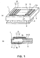
- FIG 1 is a perspective view of a liquid ejecting head according to an embodiment of the present invention, and (b) is a sectional view taken along a line A-A in (a).
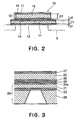
- Figure 2 is a partially sectional view of a piezoelectric structure usable for a liquid ejecting head according to the embodiment of the present invention.
- the liquid ejection recording head 1 in this embodiment comprises a plurality of liquid ejection outlets (nozzles) 2, a plurality of pressure chambers (liquid chambers) 3, a piezoelectric structure 10 provided for each of the pressure chambers 3.
- the liquid ejection outlets 2 are formed in the orifice plate 5 at predetermined intervals.
- the pressure chamber 3 is formed in the main assembly substrate portion (liquid chamber substrate) 6, corresponding to the liquid ejection outlet 2.
- the pressure chamber 3 as are connected to the respective liquid ejection outlets 2 through the liquid flow paths 6a.
- the liquid ejection outlets 2 are provided on the bottom side, the they may be provided on the lateral side.
- the piezoelectric structure 10 comprises a vibrational plate 11 and a piezoelectric element 12.
- the vibrational plate 11 constituting the piezoelectric structure 10 of this embodiment comprises monocrystal material or polycrystal material, which is sandwiched by a first oxide layer 13 and a second oxide layer 14.
- the piezoelectric film 15 of the piezoelectric element 12 constituting the piezoelectric structure 10 is made of single orientation crystal or monocrystal material.
- electrodes 16, 17 of Au, Pt one like are formed on the top and bottom sides thereof.
- the piezoelectric element 12 is constituted by the piezoelectric film 15 and the electrodes 16, 17.
- the vibratlonal plate 11 of the monocrystal polycrystal structure is sandwiched by the oxides 13, 14, and therefore, despite repeated mechanical displacements with the result of fine cracks, the vibrational plate per se is not damaged, and the adhessiveness relative to the piezoelectric film is not deteriorated. Thus, the durability is high.
- the film thicknesses are selected so as to satisfy d1+d2 ⁇ D1, where D1 is a film thickness of the vibrational plate 11, d1 is a film thickness of the first oxide layer 13, and d2 is a film thickness of the second oxide layer 14.
- D1 is a film thickness of the vibrational plate 11
- d1 is a film thickness of the first oxide layer 13
- d2 is a film thickness of the second oxide layer 14.
- the film thickness d2 is 5nm - 3 ⁇ m, preferably 10nm -1 ⁇ m.
- Film thickness D1 is 100nm -10 ⁇ m, preferably 500nm -5 ⁇ m. If the film thickness D1 of the vibrational plate 11 exceeds 10 ⁇ m, the degree of.displacement becomes insufficient for a liquid ejecting head, and therefore, it is not preferable for the high density nozzle arrangement.
- d1+d2+D1 ⁇ 5 x D2 is preferably satisfied, where D2 is a film thickness of the piezoelectric film 15.
- D2 is a film thickness of the piezoelectric film 15.
- the specific film thickness D2 of the piezoelectric film 15 is 500nm -10 ⁇ m, preferably 1 ⁇ m - 5 ⁇ m.
- the material of the vibrational plate 11 is Si, preferably monocrystal Si.
- the vibrational plate 11 may be doped with element such as B.
- the grating constant of the Si used for vibrational plate 11 may be used to provide the piezoelectric film 15 of single orientation crystal or monocrystal.
- the material of the first oxide layer 13 formed on upper may be SiO 2 , YSZ, (yttrium-stabilized zirconia), MgO or the like, and the material of the second oxide layer 14 may be at least one of SiO 2 , YSZ, Al 2 O 3 , LaAlO 3 , Ir 2 O 3 , MgO, SRO(SrRuO 3 ) STO(SrTiO 3 ) or the like.
- the material has a crystal orientation (111) or (100).
- the oxide layer is a combination of SiO 2 and another oxide
- a small amount of metal element of said another oxide may be contained to provide a preferable vibration property or the like of the vibrational plate.
- the content is not more than 10at%, preferably not more than 5at%.
- the material of the piezoelectric film 15 to be used for the piezoelectric structure 10 according to this embodiment may be, for example:
- these materials can be formed into a single orientation crystal or monocrystal film, and therefore, the performance is high.
- a rapid cooling from the film formation temperature as a rate of not less than 30°C /min. Another method is usable.
- the piezoelectric film may have a further structure of a single composition, or may be a laminated structure of two or more compositions.
- the film formation may be carried out after film formation of the anchoring layer of different material compositions.
- the film formation thereof is preferably carried out after the film formation of the anchoring layer of PbTiO 3 . It may be a composition doped with a small amount of element in the main component.
- the single orientation crystal or the monocrystal has a priority orientation degrees of the film of not less than 80%, preferably not less than 85%, and further preferably not less than 95%, as determined by XRD (X-ray diffraction apparatus) ( ⁇ - 2 ⁇ (out of plane) measurement).
- a film having a sequentially aligned crystal orientation can be formed on the substrate, and therefore, such programs do not arise.
- the variations of the ejection performance is small, and the connection strength is high.
- the film is a piezoelectric film of single orientation crystal or monocrystal, and therefore, the durability and the piezoelectric particularly property are preferable.
- the display of the layer structure is "upper electrode 17// piezoelectric film 15// lower electrode 16// second oxide layer 14// vibrational plate 11// first oxide layer 13" (reference numerals are as shown in Figure 2).
- the vibrational plate with this layer structure is Si(100), and the oxide layers sandwiching the vibrational plate is MgO(100) and SiO 2 .
- SRO has a director conductivity, and it also functions as the second oxide layer 14 and the lower electrode 16.
- the piezoelectric film is of a laminated structure of PZT for PZT/PT.
- the structure may be replaced with the layer structure of PMN, PZN, PSN, PNN, PMN-PT, PSN-PT, PZN-PT.
- the followings are usable alternatives: Au//PMN(001)//Pt(100)//MgO(100)//Si(100)//SiO 2 ; Pt//PMN- PT(001)//Pt(100)//MgO(100)/SiO 2 //Si(100)//SiO 2 ; Al//PMN- PT(001)/PT(001)//Pt(100)//YSZ(111)/SiO 2 //Si(111)//SiO 2
- the crystal orientations indicated in the parentheses in the layer structure indicate the crystal orientation having priority orientation not less than 80%, preferably not less than 85%, other preferably not less than 95%, as described hereinbefore.
- the SiO 2 which is a Si oxide film or another oxide (YSZ, MgO, Ir 2 O 3 ) may be selected depending on the manufacturing process. For example, it is possible to suppress production of SiO 2 by forming a YSZ film using the metal target during the film formation of the YSZ. By thin film film formation of metal such as Zr or the like on the Si layer, the production of SiO 2 can be prevented.
- the manufacturing method for the piezoelectric structure having the vibrational plate and the piezoelectric film comprises a step (1) of forming a second oxide layer on a silicon substrate having a monocrystal silicon layer on a silicon layer with an oxide layer interposed therebetween; a step (2) of forming a piezoelectric film of a single orientation crystal or monocrystal structure on the second oxide layer; and a step (3) of an upper electrode on the piezoelectric film.
- the silicon substrate having the monocrystal silicon layer above the silicon layer with the oxide layer therebetween may be SOI (silicon-on-insulator) substrate, or a film of monocrystal oxide may be formed on the silicon substrate, and a film of monocrystal silicon layer may be formed thereon.
- SOI substrate the oxide layer on the silicon layer is SiO 2 , for example, and the monocrystal oxide is YSZ(100), YSZ(111), MgO(100), MgO(111), STO(100), STO(111) or the like, for example.
- the film thickness (d1) of the oxide layer is 5nm - 5 ⁇ m, preferably 10nm -3 ⁇ m.
- the second oxide layer formed on the monocrystal silicon is preferably formed prior to the step (2) and/or step (3).
- the second oxide layer may be SiO 2 , YSZ(100), YSZ(111), SRO(001), SRO(111), MgO(100), MgO(111), Ir2O 3 (100), Ir2O 3 (111), Al2O 3 (100), Al2O 3 (111), LaAlO 3 (100), LaAlO 3 (111), STO(100), STO(111) or the like, for example.
- the film thicknesses (d2) of them are 5nm -3 ⁇ m, preferably 10nm -1 ⁇ m.
- the second oxide layer is MgO in example 1, and YSZ and SiO 2 in example 2.
- the SiO 2 may be produced by oxidative reaction during YSZ film formation which is a buffering film, or maybe produced by heat treatment after the film formation.
- the second oxide layer contains SiO 2
- the film thickness of SiO 2 layer can be controlled by selecting the temperature lowering process from maximum temperature of the formed YSZ film, a temperature maintaining duration thereof, a re-heat-treatment condition and a temperature maintaining duration thereof.
- the film thickness of the SiO 2 layer can be increased by the sputtering film formation temperature being maintained in the water vapor atmosphere.
- the production of the SiO 2 layer at the interface between the YSZ and the Si may be prevented by first forming a metal layer using the metal Zr target and then forming a film of YSZ. It can be selected depending on the material and the performance whether the SiO 2 layer is to be formed or not.
- a piezoelectric film having a single layer structure or a laminated structure is formed, using any of composition such as PZT, PMN, PZN, PSN, PNN, PMN-PT, PSN-PT, PZN-PT or the like.
- the piezoelectric film preferably has a single orientation crystal or monocrystal structure.
- the formation of the upper electrode on the piezoelectric film in the step (3) may be effected through a sputtering method, an evaporation method, an application method or the like.
- the electrode material may be a metal material such as Au, Pt, Cr, Al, Cu, Ir, Ni, or an electroconductive oxide such as SRO, ITO.
- the upper electrode may be a solid electrode or a comb-shaped electrode on the piezoelectric film.
- the manufacturing method for the piezoelectric structure it is possible that single orientation crystal or monocrystal piezoelectric film having a high piezoelectric constant can be formed on the silicon substrate, and therefore, a vibrational plate in which the connection strength, the durability is high, can be produced.
- a piezoelectric structure having a high frequency property, durability and electrostrictive / piezoelectric property can be provided.
- the step of separating the piezoelectric film in step (4) is a patterning step in which the piezoelectric film produced by the step (2).
- the patterning is separated corresponding to the liquid ejection outlets (nozzles) and the pressure chambers.
- the patterning method may be a wet etching type, a dry etching type, a mechanical cutting type or like.
- a protecting film formation may be carried out for the protection of the silicon substrate with the resist treatment for the patterning.
- a resin material or the like having a low rigidity not preventing expansion and contraction of the piezoelectric film may be filled between the separated piezoelectric film.
- the step (5) for forming the pressure chamber includes a process step for the silicon layer at the opposite side and/or a step of connecting a separate substrate having a formed pressure chamber portion with the silicon substrate.
- the process step for the silicon layer may be carried out through wet etching, dry etching, mechanical process (sandblast process or like).
- the substrate for said separate substrate having the pressure chamber portion may be a silicon substrate, a SUS substrate, a polymer material substrate or the like.
- the connecting method in the case of use of the silicon substrate, the SUS substrate or the like may be an anodic oxidation connection method, active metal soldering method or a method using an adhesive material. When a polymer material is used, etching process with the use of resist material is usable.
- a substrate preprocessed is usable.
- the configuration of the pressure chamber may be rectangular, circular, elliptical or the like.
- the cross-sectional configuration of the pressure chamber may be reduced toward the nozzle.
- the step (6) of forming the liquid ejection outlet may include connecting an orifice plate in which the liquid ejection outlets are formed corresponding to respective pressure chamber portions, or forming the liquid ejection outlets from resist material or the like.
- the liquid ejection outlets may be formed corresponding to the pressure chambers by laser machining.
- the forming operation may be carried out simultaneously with the step (5).
- the order of the steps (4), (5) and (6) is not limiting, and the separating step of the piezoelectric film (4) may be carried out finally.
- the piezoelectric film has a single orientation crystal or monocrystal structure, and therefore, the resultant vibrational plate has a high connection strength and durability. and therefore, it is possible to provide a liquid ejecting head having a high density, a large ejection power and a suitability to a high frequency printing.
- Figure 3 is a partially sectional view of a piezoelectric structure manufactured through a method for manufacturing the piezoelectric structure according to an embodiment of the present invention.
- a YSZ (100) 24 film having a thickness of 0.3 ⁇ m was formed on a monocrystal Si layer under 800°C through the sputtering film formation, using a SOIsubstrate constituted by a silicon layer 28 having a thickness of 625 ⁇ m, a SiO 2 layer 23 having a thickness of 0.2 ⁇ m and a monocrystal Si(100) layer 21 having a thickness of 3 ⁇ m.
- a lower electrode Pt(111) 26 was formed into a thickness of 0.5 ⁇ m, and a piezoelectric film 22 of PT(111), PZT(111) was formed under 600°C.
- the composition of PZT was Pb(Zr 0.53 Ti 0.47 )O 3 .
- the total film thickness of the piezoelectric film 22 was 3.5 ⁇ m.
- the temperature rising speed in the cooling process after the film formation was not less than 40°C /min.
- 0.02 ⁇ m thick SiO 2 layer 24a was formed as the second oxide layer at the interface between the YSZ(100) 24 and Si(100) 21.
- the film thickness of the SiO 2 layer 24a was 0.2 ⁇ m in the case that it was formed under 800°C, and then it was maintained as it is in the water vapor for 100 min.
- the contents of Y and Zr metal in the SiO 2 was 4.6at%.
- the single crystal property of the piezoelectric film 22 had not less than 99% orientation of (111) as a result of confirmation by XRD (X line diffraction apparatus).
- TMAH trimethylammonium hydroxide
- the sputtering film formation was carried out to manufacture the structure of example 2 in the above-described layer structure.
- the durability was further improved.
- the displacement measured after the etching process similarly to Embodiment 1, was 0.25 ⁇ m -0.28 ⁇ m which were preferable.
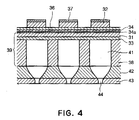
- Figure 4 is a partially sectional view of a liquid ejecting head manufactured through the manufacturing method according to the embodiment of the present invention.
- a MgO(100) 34 layer was formed into a thickness of 0.3 ⁇ m on a monocrystal Si(100) 31 having been B-doped, using a substrate 39 of a B-doped monocrystal Si(100)/SiO 2 /Si structure (film thicknesses were 2.5 ⁇ m/1 ⁇ m/250 ⁇ m). Furthermore, 0.4 ⁇ m thick of Pt(100) and a piezoelectric film 32 of PMN(001) were formed into a thickness of 2.3 ⁇ m. The composition of the PMN was adjusted by Pb(Mg 1/3 Nb 2/3 )O 3 .
- Figure 4 shows the liquid ejecting head manufactured through the method of this example, in which designated by 31 is a vibrational plate of B-doped monocrystal Si; 32 is a piezoelectric film of PMN; 33 is a first oxide layer; 34, 34a are second oxide layer; 36 lower electrode; and 37 is upper electrode.
- Designated by 38 is a Si layer in which the pressure chamber 41 is formed; 42 is a middle substrate; 43 is an orifice plate in which the liquid ejection outlets 44 are formed.
- the pressure chamber 41 has a width of 60 ⁇ m, a depth of 2.2mm, and a partition width between the adjacent pressure chambers 41 of 24 ⁇ m.
- the ink ejection tests were carried out. A maximum ejection speed of /sec was confirmed at a driving frequency of 35kHz with a driving voltage of +7V/-7V.
- the size of the droplets was controllably 3pl - 26pl.
- Durability test repeating 10 9 displacements was carried out, and the decrease of the displacement was not more than 5%.
- Two liquid ejecting heads were manufactured with the same structure except for the film thickness of the monocrystal silicon layer being 10 ⁇ m and 11 ⁇ m.
- the displacement in the liquid ejecting head having the Si layer of 10 ⁇ m thick was smaller by 10% than the liquid ejecting head having the Si layer of 2.5 ⁇ m thick, but could eject high viscosity(10cps) droplets.
- the reduction of the displacement was 17%, but it could eject the high viscosity droplets, similarly.
- the durability is slightly lower than the liquid ejecting head using 10 ⁇ m.
- the piezoelectric film in Embodiment 3 was modified by using a piezoelectric film of FSN-PT(001) (the other structures were the same).
- the composition of PSN-PT was suggested to be 0.55[Pb(Sc 1/2 Nb 1/2 )O 3 ]-0.45[PbTiO 3 ].
- the dimensions such as the width of the pressure chamber or the like were the same as in Embodiment 3. It was confirmed that ink could be ejected at a speed of 14.3m /sec with the same driving conditions. In addition, when the width of the pressure chamber was changed to 40 ⁇ m, and the length of the pressure chamber was changed to 2.5mm, and the ink could be ejected at a speed of not less than 10m /sec which is practical.
- the piezoelectric film in Embodiment 4 was changed to PZN-PT(001), without changing the other structures, and the liquid ejecting head was manufactured.
- the composition of PZN-PT was 0.90 ⁇ Pb(Zn 1/3 Nb 2/3 )O 3 ⁇ -0.10 ⁇ PbTiO 3 ⁇ .
- the ejection speed of the ink with the width of the pressure chamber being 60 ⁇ m was 14.1m /sec which was preferable.
- the quantities of the droplets were very stable.
Abstract
Description
Pt//PMN-
Al//PMN-
Claims (12)
- A piezoelectric structure comprising:a vibrational plate;a piezoelectric film;said vibrational plate including a layer of a monocrystal material, a polycrystal material, a monocrystal material doped with an element which is different from an element constituting the monocrystal material, or a polycrystal material doped with an element which is different from an element constituting the polycrystal materials, and oxide layers sandwiching the aforementioned layer,said piezoelectric film has a single orientation crystal or monocrystal structure.
- A piezoelectric structure according to Claim 1, wherein a film thickness D1 of said vibrational plate and film thicknesses d1, d2 of said oxide layers satisfy d1+d2≤ D1.
- A piezoelectric structure according to Claim 2, wherein a film thickness D2 of said piezoelectric film satisfy d1+d2+D1≤5 x D2.
- A piezoelectric structure according to Claim 1, wherein a composition of said piezoelectric film is either one of PZT, PMN, PNN, PSN, PMN-PT, PNN-PT, PSN-PT, PZN-PT, and has a single layer structure or a laminated structure of different compositions.
- A piezoelectric structure according to Claim 1, wherein said oxide layer comprises at least one of SiO2, YSZ, Al2O3, LaAlO3, Ir2O3, MgO, SRO, STO.
- A manufacturing method for manufacturing a piezoelectric structure having a vibrational plate and a piezoelectric film, said method comprising:a step of forming a second oxide layer on a silicon substrate having a monocrystal silicon layer on a silicon layer with an oxide layer interposed therebetween;a step of forming a piezoelectric film of a single orientation crystal or monocrystal structure on the second oxide layer; anda step of an upper electrode on the piezoelectric film.
- A liquid ejecting head comprising:a liquid ejection outlet;a main assembly substrate portion having a pressure chamber in fluid communication with said liquid ejection outlet and having an opening;a piezoelectric structure connected so as to plug the opening;said piezoelectric structure including,a vibrational plate;a piezoelectric film;said vibrational plate including a layer of a monocrystal material, a polycrystal material, a monocrystal material doped with an element which is different from an element constituting the monocrystal material, or a polycrystal material doped with an element which is different from an element constituting the polycrystal materials, and oxide layers sandwiching the aforementioned layer,said piezoelectric film has a single orientation crystal or monocrystal structure.
- A liquid ejecting head according to Claim 7, wherein a film thickness D1 of said vibrational plate and film thicknesses d1, d2 of said oxide layers satisfy d1+d2≤ D1.
- A liquid ejecting head according to Claim 8, wherein a film thickness D2 of said piezoelectric film satisfy d1+d2+D1≤5 x D2.
- A liquid ejection head according to Claim 6, wherein a composition of said piezoelectric film is either one of PZT, PMN, PNN, PSN, PMN-PT, PNN-PT, PSN-PT, PZN-PT, and has a single layer structure or a laminated structure of different compositions.
- A liquid ejection head according to Claim 6, wherein said oxide layer comprises at least one of SiO2, YSZ, Al2O3, LaAlO3, Ir2O3, MgO, SRO, STO.
- A manufacturing method for a liquid ejecting head including a liquid ejection outlet; a main body substrate portion having a pressure chamber in fluid communication with said liquid ejection outlet and having an opening; a piezoelectric structure connected so as to plug the opening, said manufacturing method comprising: a step of forming a second oxide layer on a silicon substrate having a monocrystal silicon layer on a silicon layer with an oxide layer interposed therebetween;
a step of forming a piezoelectric film of a single orientation crystal monocrystal structure on the second oxide layer;
a step of separating the piezoelectric film into a plurality of portions;
a step of an upper electrode on the piezoelectric film; and
a step of forming said pressure chamber.
Applications Claiming Priority (2)
| Application Number | Priority Date | Filing Date | Title |
|---|---|---|---|
| JP2001033823 | 2001-02-09 | ||
| JP2001033823A JP3833070B2 (en) | 2001-02-09 | 2001-02-09 | Liquid ejecting head and manufacturing method |
Publications (2)
| Publication Number | Publication Date |
|---|---|
| EP1231061A1 true EP1231061A1 (en) | 2002-08-14 |
| EP1231061B1 EP1231061B1 (en) | 2006-09-13 |
Family
ID=18897515
Family Applications (1)
| Application Number | Title | Priority Date | Filing Date |
|---|---|---|---|
| EP20020002903 Expired - Lifetime EP1231061B1 (en) | 2001-02-09 | 2002-02-08 | Piezoelectric structure, liquid ejecting head and manufacturing method therefor |
Country Status (7)
| Country | Link |
|---|---|
| US (2) | US7053526B2 (en) |
| EP (1) | EP1231061B1 (en) |
| JP (1) | JP3833070B2 (en) |
| KR (1) | KR100715406B1 (en) |
| CN (1) | CN1181977C (en) |
| AT (1) | ATE339313T1 (en) |
| DE (1) | DE60214612T2 (en) |
Cited By (5)
| Publication number | Priority date | Publication date | Assignee | Title |
|---|---|---|---|---|
| EP1323532A2 (en) * | 2001-12-27 | 2003-07-02 | Seiko Epson Corporation | Liquid jetting head and method of manufacturing the same |
| CN1323842C (en) * | 2004-03-11 | 2007-07-04 | 精工爱普生株式会社 | Method of manufacturing actuator device, and liquid jet device |
| US7581823B2 (en) * | 2003-12-15 | 2009-09-01 | Canon Kabushiki Kaisha | Piezoelectric film element, method of manufacturing the same, and liquid discharge head |
| EP3409476A3 (en) * | 2017-05-29 | 2019-02-13 | Seiko Epson Corporation | Piezoelectric device, liquid discharging head, and liquid discharging apparatus |
| CN112062564A (en) * | 2020-09-17 | 2020-12-11 | 广西大学 | Preparation method of PMN-PSN ultrahigh breakdown electric field thin film material |
Families Citing this family (52)
| Publication number | Priority date | Publication date | Assignee | Title |
|---|---|---|---|---|
| JP4100202B2 (en) * | 2002-03-18 | 2008-06-11 | セイコーエプソン株式会社 | Piezoelectric actuator and liquid jet head |
| JP4100953B2 (en) * | 2002-04-18 | 2008-06-11 | キヤノン株式会社 | LAMINATE HAVING SINGLE CRYSTAL OXIDE CONDUCTOR ON Si SUBSTRATE, ACTUATOR USING SAME, INKJET HEAD, AND MANUFACTURING METHOD THEREOF |
| JP4086535B2 (en) * | 2002-04-18 | 2008-05-14 | キヤノン株式会社 | Actuator and inkjet head manufacturing method |
| JP4708667B2 (en) | 2002-08-08 | 2011-06-22 | キヤノン株式会社 | Actuator and liquid jet head |
| JP2007243200A (en) * | 2002-11-11 | 2007-09-20 | Seiko Epson Corp | Piezoelectric device, liquid discharge head, ferroelectric device, electronic equipment, and method of manufacturing these |
| JP2004179642A (en) * | 2002-11-11 | 2004-06-24 | Seiko Epson Corp | Piezoelectric material device, liquid discharge head, ferroelectric device, electronic apparatus and these manufacturing methods |
| JP3821231B2 (en) | 2003-01-27 | 2006-09-13 | セイコーエプソン株式会社 | Liquid ejecting head driving method and liquid ejecting apparatus |
| CN100590902C (en) * | 2003-01-31 | 2010-02-17 | 佳能株式会社 | Piezoelectric element |
| US7215067B2 (en) * | 2003-02-07 | 2007-05-08 | Canon Kabushiki Kaisha | Ferroelectric thin film element, piezoelectric actuator and liquid discharge head |
| US7059711B2 (en) * | 2003-02-07 | 2006-06-13 | Canon Kabushiki Kaisha | Dielectric film structure, piezoelectric actuator using dielectric element film structure and ink jet head |
| JP2004255585A (en) | 2003-02-24 | 2004-09-16 | Riso Kagaku Corp | Image formation device |
| US7193756B2 (en) * | 2003-11-26 | 2007-03-20 | Matsushita Electric Industrial Co., Ltd. | Piezoelectric element, method for fabricating the same, inkjet head, method for fabricating the same, and inkjet recording apparatus |
| JP4717344B2 (en) * | 2003-12-10 | 2011-07-06 | キヤノン株式会社 | Dielectric thin film element, piezoelectric actuator, and liquid discharge head |
| US7262544B2 (en) * | 2004-01-09 | 2007-08-28 | Canon Kabushiki Kaisha | Dielectric element, piezoelectric element, ink jet head and method for producing the same head |
| JP4192794B2 (en) * | 2004-01-26 | 2008-12-10 | セイコーエプソン株式会社 | Piezoelectric element, piezoelectric actuator, ink jet recording head, ink jet printer, surface acoustic wave element, frequency filter, oscillator, electronic circuit, thin film piezoelectric resonator, and electronic device |
| TWI255057B (en) * | 2004-02-27 | 2006-05-11 | Canon Kk | Dielectric element, piezoelectric element, ink jet head and ink jet recording apparatus and manufacturing method of same |
| JP2005244133A (en) * | 2004-02-27 | 2005-09-08 | Canon Inc | Dielectric element, piezoelectric element, inkjet head, inkjet recording apparatus, and method of manufacturing the same |
| JP3875240B2 (en) | 2004-03-31 | 2007-01-31 | 株式会社東芝 | Manufacturing method of electronic parts |
| CN100568568C (en) * | 2004-04-23 | 2009-12-09 | 新加坡科技研究局 | Microelectromechanicdevices devices |
| US7497962B2 (en) | 2004-08-06 | 2009-03-03 | Canon Kabushiki Kaisha | Method of manufacturing liquid discharge head and method of manufacturing substrate for liquid discharge head |
| US7235917B2 (en) * | 2004-08-10 | 2007-06-26 | Canon Kabushiki Kaisha | Piezoelectric member element and liquid discharge head comprising element thereof |
| JP2006069152A (en) * | 2004-09-06 | 2006-03-16 | Canon Inc | Inkjet head and its manufacturing process |
| JP2006069151A (en) | 2004-09-06 | 2006-03-16 | Canon Inc | Process for fabricating piezoelectric film actuator and liquid ejection head |
| US20060219612A1 (en) * | 2005-01-28 | 2006-10-05 | Satake Usa, Inc. | Multiport ejector for use with sorter |
| US7449816B2 (en) * | 2005-03-25 | 2008-11-11 | Brother Kogyo Kabushiki Kaisha | Piezoelectric actuator, liquid transporting apparatus, and method for producing piezoelectric actuator and method for producing liquid transporting apparatus |
| US7521845B2 (en) * | 2005-08-23 | 2009-04-21 | Canon Kabushiki Kaisha | Piezoelectric substance, piezoelectric element, liquid discharge head using piezoelectric element, and liquid discharge apparatus |
| US7998362B2 (en) * | 2005-08-23 | 2011-08-16 | Canon Kabushiki Kaisha | Piezoelectric substance, piezoelectric element, liquid discharge head using piezoelectric element, liquid discharge apparatus, and production method of piezoelectric element |
| US7591543B2 (en) * | 2005-08-23 | 2009-09-22 | Canon Kabushiki Kaisha | Piezoelectric member, piezoelectric member element, liquid discharge head in use thereof, liquid discharge apparatus and method of manufacturing piezoelectric member |
| US8142678B2 (en) * | 2005-08-23 | 2012-03-27 | Canon Kabushiki Kaisha | Perovskite type oxide material, piezoelectric element, liquid discharge head and liquid discharge apparatus using the same, and method of producing perovskite type oxide material |
| WO2007023985A1 (en) | 2005-08-23 | 2007-03-01 | Canon Kabushiki Kaisha | Piezoelectric device, liquid ejecting head using same, and liquid ejector |
| US7528532B2 (en) * | 2005-08-23 | 2009-05-05 | Canon Kabushiki Kaisha | Piezoelectric substance and manufacturing method thereof, piezoelectric element and liquid discharge head using such piezoelectric element and liquid discharge apparatus |
| US20070046153A1 (en) * | 2005-08-23 | 2007-03-01 | Canon Kabushiki Kaisha | Piezoelectric substrate, piezoelectric element, liquid discharge head and liquid discharge apparatus |
| US7528530B2 (en) | 2005-08-23 | 2009-05-05 | Canon Kabushiki Kaisha | Piezoelectric substance, piezoelectric substance element, liquid discharge head, liquid discharge device and method for producing piezoelectric substance |
| US7759845B2 (en) * | 2006-03-10 | 2010-07-20 | Canon Kabushiki Kaisha | Piezoelectric substance element, liquid discharge head utilizing the same and optical element |
| JP5188076B2 (en) * | 2006-04-03 | 2013-04-24 | キヤノン株式会社 | Piezoelectric element and manufacturing method thereof, electronic device, and ink jet apparatus |
| US7984977B2 (en) * | 2006-07-14 | 2011-07-26 | Canon Kabushiki Kaisha | Piezoelectric element, manufacturing method for piezoelectric body, and liquid jet head |
| US8198199B2 (en) | 2007-03-30 | 2012-06-12 | Canon Kabushiki Kaisha | Epitaxial film, piezoelectric element, ferroelectric element, manufacturing methods of the same, and liquid discharge head |
| EP1997637B1 (en) * | 2007-05-30 | 2012-09-12 | Océ-Technologies B.V. | Method of manufacturing a piezoelectric ink jet device |
| JP5448320B2 (en) * | 2007-10-04 | 2014-03-19 | キヤノン株式会社 | Piezoelectric actuator and liquid discharge head using the same |
| JP5382905B2 (en) * | 2008-03-10 | 2014-01-08 | 富士フイルム株式会社 | Method for manufacturing piezoelectric element and method for manufacturing liquid discharge head |
| JP4618344B2 (en) * | 2008-07-29 | 2011-01-26 | コニカミノルタビジネステクノロジーズ株式会社 | Authentication device, authentication system, authentication method, authentication program, and recording medium |
| WO2011145453A1 (en) * | 2010-05-17 | 2011-11-24 | 株式会社村田製作所 | Piezoelectric actuator and drive device |
| WO2012020638A1 (en) | 2010-08-12 | 2012-02-16 | 株式会社村田製作所 | Method for manufacturing piezoelectric thin film element, piezoelectric thin film element, and member for piezoelectric thin film element |
| EP2690678B1 (en) * | 2011-03-25 | 2017-09-13 | NGK Insulators, Ltd. | Layered components and method for producing same |
| CN102794989A (en) * | 2011-05-27 | 2012-11-28 | 研能科技股份有限公司 | Piezoelectric ink jet head structure |
| CN103496257B (en) * | 2013-09-11 | 2016-01-20 | 佛山市南海金刚新材料有限公司 | Ink jet-print head and ink-jet printer |
| JP6467156B2 (en) * | 2014-07-18 | 2019-02-06 | 株式会社東芝 | Inkjet head and inkjet recording apparatus |
| CN105375812A (en) | 2014-08-13 | 2016-03-02 | 精工爱普生株式会社 | Piezoelectric driving device and driving method therefor, and robot and driving method therefor |
| JP2016040984A (en) * | 2014-08-13 | 2016-03-24 | セイコーエプソン株式会社 | Piezoelectric drive device and drive method of the same, robot and drive method of the robot |
| JP6910631B2 (en) * | 2016-11-15 | 2021-07-28 | アドバンストマテリアルテクノロジーズ株式会社 | Membrane structure and its manufacturing method |
| CN110128169B (en) * | 2019-05-10 | 2021-05-18 | 济南大学 | SiO doped with calcium ions2Method for modifying piezoelectric ceramic surface by membrane and application thereof |
| CN111081864B (en) * | 2020-01-02 | 2021-05-07 | 大连理工大学 | Preparation method of (100) preferred orientation PMN-PZT/PZT heterostructure thin film |
Citations (6)
| Publication number | Priority date | Publication date | Assignee | Title |
|---|---|---|---|---|
| EP0799700A2 (en) * | 1996-04-05 | 1997-10-08 | Seiko Epson Corporation | Ink jet recording head, its fabricating method and ink jet recording apparatus |
| JPH1044406A (en) * | 1996-08-01 | 1998-02-17 | Ricoh Co Ltd | Ink jet head and its production |
| JPH11348285A (en) | 1998-06-10 | 1999-12-21 | Matsushita Electric Ind Co Ltd | Ink jet recorder and manufacture thereof |
| GB2339724A (en) * | 1998-07-22 | 2000-02-09 | Samsung Electro Mech | Forming a piezoelectric actuator of an inkjet printhead by coating an anti-oxidation film over exposed surfaces of an integral vibrator and chamber plate |
| EP0993953A2 (en) * | 1998-10-14 | 2000-04-19 | Seiko Epson Corporation | Method for manufacturing ferroelectric thin film device, ink jet recording head, and ink jet printer |
| EP1038675A2 (en) * | 1999-03-26 | 2000-09-27 | Nec Corporation | Ink jet recording head and method for manufacture the same |
Family Cites Families (18)
| Publication number | Priority date | Publication date | Assignee | Title |
|---|---|---|---|---|
| EP0135665B1 (en) * | 1983-09-29 | 1991-07-03 | Siemens Aktiengesellschaft | Transducer plate for a piezoelectric transducer, and apparatus for manufacturing the same |
| US4783821A (en) * | 1987-11-25 | 1988-11-08 | The Regents Of The University Of California | IC processed piezoelectric microphone |
| JPH02219654A (en) * | 1989-02-20 | 1990-09-03 | Ricoh Co Ltd | Ink jet head and its manufacture |
| US5160870A (en) * | 1990-06-25 | 1992-11-03 | Carson Paul L | Ultrasonic image sensing array and method |
| US5534900A (en) * | 1990-09-21 | 1996-07-09 | Seiko Epson Corporation | Ink-jet recording apparatus |
| WO1993022140A1 (en) * | 1992-04-23 | 1993-11-11 | Seiko Epson Corporation | Liquid jet head and production thereof |
| US5719607A (en) | 1994-08-25 | 1998-02-17 | Seiko Epson Corporation | Liquid jet head |
| JP3381473B2 (en) * | 1994-08-25 | 2003-02-24 | セイコーエプソン株式会社 | Liquid jet head |
| EP0736385B1 (en) * | 1995-04-03 | 1998-02-25 | Seiko Epson Corporation | Printer head for ink jet recording and process for the preparation thereof |
| JP3327149B2 (en) * | 1995-12-20 | 2002-09-24 | セイコーエプソン株式会社 | Piezoelectric thin film element and ink jet recording head using the same |
| US5804907A (en) | 1997-01-28 | 1998-09-08 | The Penn State Research Foundation | High strain actuator using ferroelectric single crystal |
| JP3832075B2 (en) * | 1997-03-25 | 2006-10-11 | セイコーエプソン株式会社 | Inkjet recording head, method for manufacturing the same, and piezoelectric element |
| JP3666177B2 (en) * | 1997-04-14 | 2005-06-29 | 松下電器産業株式会社 | Inkjet recording device |
| US6331259B1 (en) * | 1997-12-05 | 2001-12-18 | Canon Kabushiki Kaisha | Method for manufacturing ink jet recording heads |
| KR100464307B1 (en) * | 1998-10-16 | 2005-02-28 | 삼성전자주식회사 | A piezo-electric ink-jet printhead and a fabricating method thereof |
| JP2000357826A (en) * | 1999-04-13 | 2000-12-26 | Seiko Epson Corp | Manufacture of piezoelectric element, piezoelectric element, ink-jet type memory head and printer |
| JP3796394B2 (en) * | 2000-06-21 | 2006-07-12 | キヤノン株式会社 | Method for manufacturing piezoelectric element and method for manufacturing liquid jet recording head |
| JP3754897B2 (en) * | 2001-02-09 | 2006-03-15 | キヤノン株式会社 | Semiconductor device substrate and method for manufacturing SOI substrate |
-
2001
- 2001-02-09 JP JP2001033823A patent/JP3833070B2/en not_active Expired - Lifetime
-
2002
- 2002-02-08 EP EP20020002903 patent/EP1231061B1/en not_active Expired - Lifetime
- 2002-02-08 DE DE2002614612 patent/DE60214612T2/en not_active Expired - Lifetime
- 2002-02-08 AT AT02002903T patent/ATE339313T1/en not_active IP Right Cessation
- 2002-02-09 CN CNB021217092A patent/CN1181977C/en not_active Expired - Lifetime
- 2002-02-09 KR KR20020007658A patent/KR100715406B1/en active IP Right Grant
- 2002-02-11 US US10/071,095 patent/US7053526B2/en not_active Expired - Lifetime
-
2005
- 2005-10-03 US US11/240,524 patent/US7069631B2/en not_active Expired - Lifetime
Patent Citations (6)
| Publication number | Priority date | Publication date | Assignee | Title |
|---|---|---|---|---|
| EP0799700A2 (en) * | 1996-04-05 | 1997-10-08 | Seiko Epson Corporation | Ink jet recording head, its fabricating method and ink jet recording apparatus |
| JPH1044406A (en) * | 1996-08-01 | 1998-02-17 | Ricoh Co Ltd | Ink jet head and its production |
| JPH11348285A (en) | 1998-06-10 | 1999-12-21 | Matsushita Electric Ind Co Ltd | Ink jet recorder and manufacture thereof |
| GB2339724A (en) * | 1998-07-22 | 2000-02-09 | Samsung Electro Mech | Forming a piezoelectric actuator of an inkjet printhead by coating an anti-oxidation film over exposed surfaces of an integral vibrator and chamber plate |
| EP0993953A2 (en) * | 1998-10-14 | 2000-04-19 | Seiko Epson Corporation | Method for manufacturing ferroelectric thin film device, ink jet recording head, and ink jet printer |
| EP1038675A2 (en) * | 1999-03-26 | 2000-09-27 | Nec Corporation | Ink jet recording head and method for manufacture the same |
Non-Patent Citations (1)
| Title |
|---|
| PATENT ABSTRACTS OF JAPAN vol. 1998, no. 06 30 April 1998 (1998-04-30) * |
Cited By (9)
| Publication number | Priority date | Publication date | Assignee | Title |
|---|---|---|---|---|
| EP1323532A2 (en) * | 2001-12-27 | 2003-07-02 | Seiko Epson Corporation | Liquid jetting head and method of manufacturing the same |
| EP1323532A3 (en) * | 2001-12-27 | 2003-09-03 | Seiko Epson Corporation | Liquid jetting head and method of manufacturing the same |
| US7246888B2 (en) | 2001-12-27 | 2007-07-24 | Seiko Epson Corporation | Liquid jetting head and method of manufacturing the same |
| US7581823B2 (en) * | 2003-12-15 | 2009-09-01 | Canon Kabushiki Kaisha | Piezoelectric film element, method of manufacturing the same, and liquid discharge head |
| CN1323842C (en) * | 2004-03-11 | 2007-07-04 | 精工爱普生株式会社 | Method of manufacturing actuator device, and liquid jet device |
| EP3409476A3 (en) * | 2017-05-29 | 2019-02-13 | Seiko Epson Corporation | Piezoelectric device, liquid discharging head, and liquid discharging apparatus |
| US10639893B2 (en) | 2017-05-29 | 2020-05-05 | Seiko Epson Corporation | Piezoelectric device, liquid discharging head, and liquid discharging apparatus |
| CN112062564A (en) * | 2020-09-17 | 2020-12-11 | 广西大学 | Preparation method of PMN-PSN ultrahigh breakdown electric field thin film material |
| CN112062564B (en) * | 2020-09-17 | 2022-05-17 | 广西大学 | Preparation method of PMN-PSN ultrahigh breakdown electric field thin film material |
Also Published As
| Publication number | Publication date |
|---|---|
| US20020140320A1 (en) | 2002-10-03 |
| ATE339313T1 (en) | 2006-10-15 |
| JP3833070B2 (en) | 2006-10-11 |
| DE60214612D1 (en) | 2006-10-26 |
| JP2002234156A (en) | 2002-08-20 |
| US20060028100A1 (en) | 2006-02-09 |
| DE60214612T2 (en) | 2007-09-27 |
| US7053526B2 (en) | 2006-05-30 |
| CN1181977C (en) | 2004-12-29 |
| EP1231061B1 (en) | 2006-09-13 |
| CN1380187A (en) | 2002-11-20 |
| US7069631B2 (en) | 2006-07-04 |
| KR100715406B1 (en) | 2007-05-08 |
| KR20020066226A (en) | 2002-08-14 |
Similar Documents
| Publication | Publication Date | Title |
|---|---|---|
| EP1231061B1 (en) | Piezoelectric structure, liquid ejecting head and manufacturing method therefor | |
| KR100485551B1 (en) | Structure of piezoelectric element and liquid discharge recording head, and method of manufacture therefor | |
| EP1560278B1 (en) | Dielectric element, piezoelectric element, ink jet head and method for producing the same head | |
| EP1707368B1 (en) | Piezoelectric element, liquid-jet head and liquid-jet apparatus | |
| JP4717344B2 (en) | Dielectric thin film element, piezoelectric actuator, and liquid discharge head | |
| CN100590902C (en) | Piezoelectric element | |
| US7768178B2 (en) | Piezoelectric device, piezoelectric actuator, and liquid discharge device having piezoelectric films | |
| EP2044245B1 (en) | Piezoelectric substance, piezoelectric element, and liquid discharge head and liquid discharge apparatus using piezoelectric element | |
| US7827658B2 (en) | Method for manufacturing actuator device and liquid ejecting head including actuator device prepared by the method | |
| EP1968128B1 (en) | Piezoelectric device, process for producing the same, and liquid discharge device | |
| JP2005175099A5 (en) | ||
| US8591011B2 (en) | Piezoelectric element, actuator device, liquid ejecting head, and liquid ejecting apparatus | |
| US7045935B2 (en) | Actuator and liquid discharge head, and method for manufacturing liquid discharge head | |
| US7193756B2 (en) | Piezoelectric element, method for fabricating the same, inkjet head, method for fabricating the same, and inkjet recording apparatus | |
| EP1029679A1 (en) | Ink jet recording head and ink jet recording apparatus incorporating the same | |
| JP2001260348A (en) | Ink jet recording head and ink jet recorder | |
| EP3424719B1 (en) | Piezoelectric device, liquid ejecting head, and liquid ejecting apparatus | |
| KR20030038788A (en) | Piezoelectric thin film and method for preparation thereof, and piezoelectric element having the piezoelectric thin film, ink-jet head using the piezoelectric element, and ink-jet recording device having the ink-jet head | |
| JP4086864B2 (en) | Method for manufacturing liquid discharge head and method for manufacturing substrate for liquid discharge head | |
| EP3828944A1 (en) | Method for producing a piezoelectric actuator | |
| US11878526B2 (en) | Liquid ejecting head and liquid ejecting apparatus | |
| US8210659B2 (en) | Liquid ejecting head, liquid ejecting apparatus, and piezoelectric element | |
| JP2005353746A (en) | Actuator and ink jet head | |
| JP2004351878A (en) | Piezoelectric inkjet head | |
| JP2004071945A (en) | Actuators and liquid jet head |
Legal Events
| Date | Code | Title | Description |
|---|---|---|---|
| PUAI | Public reference made under article 153(3) epc to a published international application that has entered the european phase |
Free format text: ORIGINAL CODE: 0009012 |
|
| AK | Designated contracting states |
Kind code of ref document: A1 Designated state(s): AT BE CH CY DE DK ES FI FR GB GR IE IT LI LU MC NL PT SE TR |
|
| AX | Request for extension of the european patent |
Free format text: AL;LT;LV;MK;RO;SI |
|
| 17P | Request for examination filed |
Effective date: 20030107 |
|
| AKX | Designation fees paid |
Designated state(s): AT BE CH CY DE DK ES FI FR GB GR IE IT LI LU MC NL PT SE TR |
|
| 17Q | First examination report despatched |
Effective date: 20050112 |
|
| GRAP | Despatch of communication of intention to grant a patent |
Free format text: ORIGINAL CODE: EPIDOSNIGR1 |
|
| GRAS | Grant fee paid |
Free format text: ORIGINAL CODE: EPIDOSNIGR3 |
|
| GRAA | (expected) grant |
Free format text: ORIGINAL CODE: 0009210 |
|
| AK | Designated contracting states |
Kind code of ref document: B1 Designated state(s): AT BE CH CY DE DK ES FI FR GB GR IE IT LI LU MC NL PT SE TR |
|
| PG25 | Lapsed in a contracting state [announced via postgrant information from national office to epo] |
Ref country code: IT Free format text: LAPSE BECAUSE OF FAILURE TO SUBMIT A TRANSLATION OF THE DESCRIPTION OR TO PAY THE FEE WITHIN THE PRESCRIBED TIME-LIMIT;WARNING: LAPSES OF ITALIAN PATENTS WITH EFFECTIVE DATE BEFORE 2007 MAY HAVE OCCURRED AT ANY TIME BEFORE 2007. THE CORRECT EFFECTIVE DATE MAY BE DIFFERENT FROM THE ONE RECORDED. Effective date: 20060913 Ref country code: CH Free format text: LAPSE BECAUSE OF FAILURE TO SUBMIT A TRANSLATION OF THE DESCRIPTION OR TO PAY THE FEE WITHIN THE PRESCRIBED TIME-LIMIT Effective date: 20060913 Ref country code: FI Free format text: LAPSE BECAUSE OF FAILURE TO SUBMIT A TRANSLATION OF THE DESCRIPTION OR TO PAY THE FEE WITHIN THE PRESCRIBED TIME-LIMIT Effective date: 20060913 Ref country code: AT Free format text: LAPSE BECAUSE OF FAILURE TO SUBMIT A TRANSLATION OF THE DESCRIPTION OR TO PAY THE FEE WITHIN THE PRESCRIBED TIME-LIMIT Effective date: 20060913 Ref country code: BE Free format text: LAPSE BECAUSE OF FAILURE TO SUBMIT A TRANSLATION OF THE DESCRIPTION OR TO PAY THE FEE WITHIN THE PRESCRIBED TIME-LIMIT Effective date: 20060913 Ref country code: LI Free format text: LAPSE BECAUSE OF FAILURE TO SUBMIT A TRANSLATION OF THE DESCRIPTION OR TO PAY THE FEE WITHIN THE PRESCRIBED TIME-LIMIT Effective date: 20060913 Ref country code: NL Free format text: LAPSE BECAUSE OF FAILURE TO SUBMIT A TRANSLATION OF THE DESCRIPTION OR TO PAY THE FEE WITHIN THE PRESCRIBED TIME-LIMIT Effective date: 20060913 |
|
| REG | Reference to a national code |
Ref country code: GB Ref legal event code: FG4D |
|
| REG | Reference to a national code |
Ref country code: CH Ref legal event code: EP |
|
| REG | Reference to a national code |
Ref country code: IE Ref legal event code: FG4D |
|
| REF | Corresponds to: |
Ref document number: 60214612 Country of ref document: DE Date of ref document: 20061026 Kind code of ref document: P |
|
| PG25 | Lapsed in a contracting state [announced via postgrant information from national office to epo] |
Ref country code: SE Free format text: LAPSE BECAUSE OF FAILURE TO SUBMIT A TRANSLATION OF THE DESCRIPTION OR TO PAY THE FEE WITHIN THE PRESCRIBED TIME-LIMIT Effective date: 20061213 Ref country code: DK Free format text: LAPSE BECAUSE OF FAILURE TO SUBMIT A TRANSLATION OF THE DESCRIPTION OR TO PAY THE FEE WITHIN THE PRESCRIBED TIME-LIMIT Effective date: 20061213 |
|
| PG25 | Lapsed in a contracting state [announced via postgrant information from national office to epo] |
Ref country code: ES Free format text: LAPSE BECAUSE OF FAILURE TO SUBMIT A TRANSLATION OF THE DESCRIPTION OR TO PAY THE FEE WITHIN THE PRESCRIBED TIME-LIMIT Effective date: 20061224 |
|
| PG25 | Lapsed in a contracting state [announced via postgrant information from national office to epo] |
Ref country code: PT Free format text: LAPSE BECAUSE OF FAILURE TO SUBMIT A TRANSLATION OF THE DESCRIPTION OR TO PAY THE FEE WITHIN THE PRESCRIBED TIME-LIMIT Effective date: 20070226 |
|
| PG25 | Lapsed in a contracting state [announced via postgrant information from national office to epo] |
Ref country code: MC Free format text: LAPSE BECAUSE OF NON-PAYMENT OF DUE FEES Effective date: 20070228 |
|
| NLV1 | Nl: lapsed or annulled due to failure to fulfill the requirements of art. 29p and 29m of the patents act | ||
| REG | Reference to a national code |
Ref country code: CH Ref legal event code: PL |
|
| ET | Fr: translation filed | ||
| PLBE | No opposition filed within time limit |
Free format text: ORIGINAL CODE: 0009261 |
|
| STAA | Information on the status of an ep patent application or granted ep patent |
Free format text: STATUS: NO OPPOSITION FILED WITHIN TIME LIMIT |
|
| 26N | No opposition filed |
Effective date: 20070614 |
|
| PG25 | Lapsed in a contracting state [announced via postgrant information from national office to epo] |
Ref country code: IE Free format text: LAPSE BECAUSE OF NON-PAYMENT OF DUE FEES Effective date: 20070208 |
|
| PG25 | Lapsed in a contracting state [announced via postgrant information from national office to epo] |
Ref country code: GR Free format text: LAPSE BECAUSE OF FAILURE TO SUBMIT A TRANSLATION OF THE DESCRIPTION OR TO PAY THE FEE WITHIN THE PRESCRIBED TIME-LIMIT Effective date: 20061214 |
|
| PG25 | Lapsed in a contracting state [announced via postgrant information from national office to epo] |
Ref country code: LU Free format text: LAPSE BECAUSE OF NON-PAYMENT OF DUE FEES Effective date: 20070208 Ref country code: CY Free format text: LAPSE BECAUSE OF FAILURE TO SUBMIT A TRANSLATION OF THE DESCRIPTION OR TO PAY THE FEE WITHIN THE PRESCRIBED TIME-LIMIT Effective date: 20060913 |
|
| PG25 | Lapsed in a contracting state [announced via postgrant information from national office to epo] |
Ref country code: TR Free format text: LAPSE BECAUSE OF FAILURE TO SUBMIT A TRANSLATION OF THE DESCRIPTION OR TO PAY THE FEE WITHIN THE PRESCRIBED TIME-LIMIT Effective date: 20060913 |
|
| REG | Reference to a national code |
Ref country code: FR Ref legal event code: PLFP Year of fee payment: 15 |
|
| REG | Reference to a national code |
Ref country code: FR Ref legal event code: PLFP Year of fee payment: 16 |
|
| REG | Reference to a national code |
Ref country code: FR Ref legal event code: PLFP Year of fee payment: 17 |
|
| PGFP | Annual fee paid to national office [announced via postgrant information from national office to epo] |
Ref country code: FR Payment date: 20210120 Year of fee payment: 20 |
|
| PGFP | Annual fee paid to national office [announced via postgrant information from national office to epo] |
Ref country code: DE Payment date: 20210120 Year of fee payment: 20 Ref country code: GB Payment date: 20210120 Year of fee payment: 20 |
|
| PGFP | Annual fee paid to national office [announced via postgrant information from national office to epo] |
Ref country code: IT Payment date: 20210120 Year of fee payment: 20 |
|
| REG | Reference to a national code |
Ref country code: GB Ref legal event code: PE20 Expiry date: 20220207 |
|
| PG25 | Lapsed in a contracting state [announced via postgrant information from national office to epo] |
Ref country code: GB Free format text: LAPSE BECAUSE OF EXPIRATION OF PROTECTION Effective date: 20220207 |