EP1239513A2 - Manufacturing method of semiconductor device - Google Patents
Manufacturing method of semiconductor device Download PDFInfo
- Publication number
- EP1239513A2 EP1239513A2 EP02251663A EP02251663A EP1239513A2 EP 1239513 A2 EP1239513 A2 EP 1239513A2 EP 02251663 A EP02251663 A EP 02251663A EP 02251663 A EP02251663 A EP 02251663A EP 1239513 A2 EP1239513 A2 EP 1239513A2
- Authority
- EP
- European Patent Office
- Prior art keywords
- polycrystalline silicon
- cleaning
- forming
- cleansing agent
- contact hole
- Prior art date
- Legal status (The legal status is an assumption and is not a legal conclusion. Google has not performed a legal analysis and makes no representation as to the accuracy of the status listed.)
- Granted
Links
- 238000004519 manufacturing process Methods 0.000 title claims abstract description 27
- 239000004065 semiconductor Substances 0.000 title claims abstract description 13
- 229910021420 polycrystalline silicon Inorganic materials 0.000 claims abstract description 101
- 238000004140 cleaning Methods 0.000 claims abstract description 47
- 239000000758 substrate Substances 0.000 claims abstract description 38
- 239000003599 detergent Substances 0.000 claims abstract description 35
- 239000002019 doping agent Substances 0.000 claims abstract description 35
- 238000010438 heat treatment Methods 0.000 claims abstract description 25
- MHAJPDPJQMAIIY-UHFFFAOYSA-N Hydrogen peroxide Chemical compound OO MHAJPDPJQMAIIY-UHFFFAOYSA-N 0.000 claims abstract description 15
- XLYOFNOQVPJJNP-UHFFFAOYSA-N water Substances O XLYOFNOQVPJJNP-UHFFFAOYSA-N 0.000 claims abstract description 11
- QGZKDVFQNNGYKY-UHFFFAOYSA-N Ammonia Chemical compound N QGZKDVFQNNGYKY-UHFFFAOYSA-N 0.000 claims abstract description 10
- 229910021529 ammonia Inorganic materials 0.000 claims abstract description 5
- 238000000034 method Methods 0.000 claims description 48
- 239000002585 base Substances 0.000 claims description 47
- KRHYYFGTRYWZRS-UHFFFAOYSA-N Fluorane Chemical compound F KRHYYFGTRYWZRS-UHFFFAOYSA-N 0.000 claims description 26
- 238000005530 etching Methods 0.000 claims description 21
- 239000007800 oxidant agent Substances 0.000 claims description 21
- 230000001590 oxidative effect Effects 0.000 claims description 20
- XUIMIQQOPSSXEZ-UHFFFAOYSA-N Silicon Chemical compound [Si] XUIMIQQOPSSXEZ-UHFFFAOYSA-N 0.000 claims description 17
- 229910052710 silicon Inorganic materials 0.000 claims description 17
- 239000010703 silicon Substances 0.000 claims description 17
- 239000003513 alkali Substances 0.000 claims description 16
- 238000011282 treatment Methods 0.000 claims description 16
- 150000003839 salts Chemical class 0.000 claims description 10
- 239000002253 acid Substances 0.000 claims description 6
- 238000007493 shaping process Methods 0.000 claims description 5
- 238000000137 annealing Methods 0.000 claims description 4
- 230000002547 anomalous effect Effects 0.000 abstract description 14
- 238000002425 crystallisation Methods 0.000 abstract description 11
- 238000001312 dry etching Methods 0.000 abstract description 7
- 239000010408 film Substances 0.000 description 122
- 238000009792 diffusion process Methods 0.000 description 26
- 229920005591 polysilicon Polymers 0.000 description 26
- VYPSYNLAJGMNEJ-UHFFFAOYSA-N Silicium dioxide Chemical compound O=[Si]=O VYPSYNLAJGMNEJ-UHFFFAOYSA-N 0.000 description 16
- 229910052814 silicon oxide Inorganic materials 0.000 description 16
- ZOXJGFHDIHLPTG-UHFFFAOYSA-N Boron Chemical compound [B] ZOXJGFHDIHLPTG-UHFFFAOYSA-N 0.000 description 7
- 229910052796 boron Inorganic materials 0.000 description 7
- 229910052785 arsenic Inorganic materials 0.000 description 6
- RQNWIZPPADIBDY-UHFFFAOYSA-N arsenic atom Chemical compound [As] RQNWIZPPADIBDY-UHFFFAOYSA-N 0.000 description 6
- 239000013078 crystal Substances 0.000 description 6
- 239000012299 nitrogen atmosphere Substances 0.000 description 6
- 239000010409 thin film Substances 0.000 description 6
- 230000000694 effects Effects 0.000 description 5
- 239000007790 solid phase Substances 0.000 description 5
- VEXZGXHMUGYJMC-UHFFFAOYSA-N Hydrochloric acid Chemical compound Cl VEXZGXHMUGYJMC-UHFFFAOYSA-N 0.000 description 4
- QAOWNCQODCNURD-UHFFFAOYSA-N Sulfuric acid Chemical compound OS(O)(=O)=O QAOWNCQODCNURD-UHFFFAOYSA-N 0.000 description 4
- 238000007796 conventional method Methods 0.000 description 4
- 230000000977 initiatory effect Effects 0.000 description 4
- 230000003647 oxidation Effects 0.000 description 4
- 238000007254 oxidation reaction Methods 0.000 description 4
- 230000003321 amplification Effects 0.000 description 3
- 238000004380 ashing Methods 0.000 description 3
- 239000003795 chemical substances by application Substances 0.000 description 3
- 238000000151 deposition Methods 0.000 description 3
- 230000008021 deposition Effects 0.000 description 3
- 238000005516 engineering process Methods 0.000 description 3
- 238000011068 loading method Methods 0.000 description 3
- 238000004518 low pressure chemical vapour deposition Methods 0.000 description 3
- 238000003199 nucleic acid amplification method Methods 0.000 description 3
- 238000004151 rapid thermal annealing Methods 0.000 description 3
- 230000015572 biosynthetic process Effects 0.000 description 2
- 229910052751 metal Inorganic materials 0.000 description 2
- 239000002184 metal Substances 0.000 description 2
- 238000001020 plasma etching Methods 0.000 description 2
- 230000001105 regulatory effect Effects 0.000 description 2
- 230000003746 surface roughness Effects 0.000 description 2
- WFKWXMTUELFFGS-UHFFFAOYSA-N tungsten Chemical compound [W] WFKWXMTUELFFGS-UHFFFAOYSA-N 0.000 description 2
- 229910052721 tungsten Inorganic materials 0.000 description 2
- 239000010937 tungsten Substances 0.000 description 2
- OAICVXFJPJFONN-UHFFFAOYSA-N Phosphorus Chemical compound [P] OAICVXFJPJFONN-UHFFFAOYSA-N 0.000 description 1
- 229910052799 carbon Inorganic materials 0.000 description 1
- 239000012459 cleaning agent Substances 0.000 description 1
- 230000007423 decrease Effects 0.000 description 1
- 230000008034 disappearance Effects 0.000 description 1
- 238000011156 evaluation Methods 0.000 description 1
- 229910052739 hydrogen Inorganic materials 0.000 description 1
- 239000001257 hydrogen Substances 0.000 description 1
- 125000004435 hydrogen atom Chemical group [H]* 0.000 description 1
- 230000002209 hydrophobic effect Effects 0.000 description 1
- 238000005468 ion implantation Methods 0.000 description 1
- 238000002955 isolation Methods 0.000 description 1
- 229910021421 monocrystalline silicon Inorganic materials 0.000 description 1
- 230000003071 parasitic effect Effects 0.000 description 1
- 238000000059 patterning Methods 0.000 description 1
- 229910052698 phosphorus Inorganic materials 0.000 description 1
- 239000011574 phosphorus Substances 0.000 description 1
- 239000003870 refractory metal Substances 0.000 description 1
- 238000006467 substitution reaction Methods 0.000 description 1
Images


Classifications
-
- H—ELECTRICITY
- H01—ELECTRIC ELEMENTS
- H01L—SEMICONDUCTOR DEVICES NOT COVERED BY CLASS H10
- H01L29/00—Semiconductor devices adapted for rectifying, amplifying, oscillating or switching, or capacitors or resistors with at least one potential-jump barrier or surface barrier, e.g. PN junction depletion layer or carrier concentration layer; Details of semiconductor bodies or of electrodes thereof ; Multistep manufacturing processes therefor
- H01L29/66—Types of semiconductor device ; Multistep manufacturing processes therefor
- H01L29/66007—Multistep manufacturing processes
- H01L29/66075—Multistep manufacturing processes of devices having semiconductor bodies comprising group 14 or group 13/15 materials
- H01L29/66227—Multistep manufacturing processes of devices having semiconductor bodies comprising group 14 or group 13/15 materials the devices being controllable only by the electric current supplied or the electric potential applied, to an electrode which does not carry the current to be rectified, amplified or switched, e.g. three-terminal devices
- H01L29/66234—Bipolar junction transistors [BJT]
- H01L29/66272—Silicon vertical transistors
- H01L29/66287—Silicon vertical transistors with a single crystalline emitter, collector or base including extrinsic, link or graft base formed on the silicon substrate, e.g. by epitaxy, recrystallisation, after insulating device isolation
-
- H—ELECTRICITY
- H01—ELECTRIC ELEMENTS
- H01L—SEMICONDUCTOR DEVICES NOT COVERED BY CLASS H10
- H01L21/00—Processes or apparatus adapted for the manufacture or treatment of semiconductor or solid state devices or of parts thereof
- H01L21/02—Manufacture or treatment of semiconductor devices or of parts thereof
- H01L21/02041—Cleaning
- H01L21/02043—Cleaning before device manufacture, i.e. Begin-Of-Line process
- H01L21/02052—Wet cleaning only
-
- H—ELECTRICITY
- H01—ELECTRIC ELEMENTS
- H01L—SEMICONDUCTOR DEVICES NOT COVERED BY CLASS H10
- H01L21/00—Processes or apparatus adapted for the manufacture or treatment of semiconductor or solid state devices or of parts thereof
- H01L21/02—Manufacture or treatment of semiconductor devices or of parts thereof
- H01L21/04—Manufacture or treatment of semiconductor devices or of parts thereof the devices having at least one potential-jump barrier or surface barrier, e.g. PN junction, depletion layer or carrier concentration layer
- H01L21/18—Manufacture or treatment of semiconductor devices or of parts thereof the devices having at least one potential-jump barrier or surface barrier, e.g. PN junction, depletion layer or carrier concentration layer the devices having semiconductor bodies comprising elements of Group IV of the Periodic System or AIIIBV compounds with or without impurities, e.g. doping materials
- H01L21/30—Treatment of semiconductor bodies using processes or apparatus not provided for in groups H01L21/20 - H01L21/26
- H01L21/31—Treatment of semiconductor bodies using processes or apparatus not provided for in groups H01L21/20 - H01L21/26 to form insulating layers thereon, e.g. for masking or by using photolithographic techniques; After treatment of these layers; Selection of materials for these layers
- H01L21/3105—After-treatment
- H01L21/311—Etching the insulating layers by chemical or physical means
- H01L21/31105—Etching inorganic layers
- H01L21/31111—Etching inorganic layers by chemical means
- H01L21/31116—Etching inorganic layers by chemical means by dry-etching
Definitions
- the present invention relates to a process for manufacturing a bipolar transistor.
- the structures of bipolar transistors can be classified into two groups; a conventional type and a SST (Super Self-alignment Technology) type.
- the structure referred to the conventional type is generally made by forming a collector region and a base region in a substrate by the ion implantation technology or the like, and thereafter forming an emitter electrode above it and diffusing thermally dopants from this emitter electrode to form an emitter region in the base region.
- SST Super Self-alignment Technology
- n-type dopants are ion-implanted into the surface of a p-type silicon substrate 1 to form a collector region 2, and p-type dopants are then ion-implanted to form a base region 3 on the surface of the collector region 2.
- an insulating film 4 and a first polycrystalline silicon film 5 are grown in this order (Fig. 7(b)).
- a resist 6 having an opening is formed (Fig. 7(c)), and using this resist as a mask, a contact hole to reach the base region is formed by means of dry etching. In this state, 7 may attach onto the inside of the contact hole (Fig. 7(d)).
- ashing and a treatment with a resist-peeling agent are carried out, and then a cleaning using hydrofluoric acid or its salt is carried out, and followed by a rinsing with pure water.
- a cleaning using hydrofluoric acid or its salt is carried out, and followed by a rinsing with pure water.
- anomalous bodies 8 derived from the remnant solution of hydrofluoric acid after rinsing may reattach onto the first polycrystalline silicon film 5 and the inside of the contact hole (Fig. 8(a)).
- n-type dopants are ion-implanted into the second polycrystalline silicon film 11 and, then, by applying a heat treatment to the whole substrate, the n-type dopants are made to diffuse into the base region 3 to form an emitter region 14.
- the first polycrystalline silicon film 5 and the second polycrystalline silicon film 11 are shaped into an emitter electrode 15 by selective dry etching, whereby a bipolar transistor is accomplished (Fig. 8(b)).
- anomalous bodies 8 derived from the remnant solution of hydrofluoric acid after rinsing may reattach onto the first polycrystalline silicon film 5 and the inside of the contact hole, as shown in Fig. 8(a).
- anomalous bodies 8 derived from the remnant solution of hydrofluoric acid after rinsing may reattach onto the first polycrystalline silicon film 5 and the inside of the contact hole, as shown in Fig. 8(a).
- anomalous bodies 8 happen to remain also on the interface between the emitter electrode 15 and the base region 3, they lead to incomplete diffusion of emitter dopants, and thus in some cases, the emitter region may fail to be formed as designed or the emitter electrode resistance may become high.
- SST Super Self-alignment Technology
- an outer base region is formed around an emitter in the manner of self-alignment and connected to a base electrode through a polycrystalline silicon film. It is deferent from the afore-mentioned conventional structure that a polysilicon film for lead of the base is formed on a substrate and a plurality of heat treatments are required to form a base region by thermal diffusion.
- Fig. 5 is a process for manufacturing a bipolar transistor with a SST structure, disclosed in Japanese Patent Application Laid-open No. 6-69225.
- an element isolation oxide film 504 is formed on an epitaxial substrate, wherein an n + collector buried layer 502 and n - collector epitaxial layer 503 are formed on a p-type silicon substrate 501.
- a silicon oxide film 506 is grown and, in a region where an emitter is to be formed, an opening is formed through the silicon oxide film 506 and the p + -type base polysilicon film 505 to expose the n - collector epitaxial layer 503 (Fig.
- a silicon oxide film is grown over the entire surface and this oxide film is etched by anisotropic etching such as the RIE (Reactive Ion Etching) to form sidewalls 507 of the silicon oxide film.
- a heat treatment is then applied thereto in a nitrogen atmosphere to form p + -type outer base diffusion region 508 (Fig. 5(b)).
- a polysilicon film 509 that is to serve as an emitter electrode is grown under such a condition that loading of polysilicon deposition apparatus at low temperature or while making hydrogen substitution may allow only little natural oxide film to grow on the interface with the epitaxial layer 503, and then boron 510 is ion-implanted into this polysilicon film 509.
- boron is made to make solid phase diffusion from the emitter polysilicon film 509 to the n - epitaxial layer 503 to form a boron diffusion region 511 that is to serve as an inner base diffusion region (Fig. 5(c)).
- arsenic 512 is ion-implanted into the polysilicon film 509 and then, by applying a lamp heating thereto, for example, at 1050 °C for 10 seconds in a nitrogen atmosphere, arsenic is made also to make solid phase diffusion from the emitter polysilicon film 509 to the n - epitaxial layer 503 to form an emitter diffusion region 513 as well as a base diffusion region 511' in the manner of self-alignment (Fig. 5(d)).
- the emitter polysilicon film 509 is then shaped into an emitter polysilicon electrode 509 by patterning.
- a metal electrode 514 is plated over the emitter polysilicon electrode 509' and the polysilicon electrode 505 for lead of the base and, then, patterned (Fig. 5(e)).
- the above process employing the double diffusion method prevent any oxide film from growing on the epitaxial layer 503, but repeated lamp annealing results in the enlargement of crystalline grains in the emitter polysilicon film 509 that is the very source of diffusion.
- This single-crystallization event makes it hard to control the concentrations of the dopants and the depth in the emitter-base junction section, and thus bringing about deviation in the diffusion profile.
- the publication set forth discloses another process for manufacturing, as shown in Fig. 6.
- the fabrication steps proceeds up to the step of forming a P + diffusion region 103.
- conditions of pretreatment, loading into a deposition furnace and the like are to be regulated so that such an oxide film 105 as a natural oxide film of a thickness not less than 5 angstroms but not more than 20 angstroms will be formed on the surface that is to become the interface between an epitaxial layer 101 and an emitter polysilicon layer 104 (Fig. 6(a)).
- an emitter polysilicon film 104 is grown over the entire surface of the epitaxial layer 101 (Fig. 6(b)).
- boron 106 is ion-implanted into this emitter polysilicon film 104 (Fig. 6(c)).
- a heating in a furnace thereto for example, at 900 °C for 20 minutes in a nitrogen atmosphere, boron is then made to make solid phase diffusion from the emitter polysilicon film 104 to the n - epitaxial layer to form a boron diffusion region 107, and so as to prevent the emitter polysilicon film 104 from single-crystallizing by the solid phase epitaxial growth.
- arsenic 108 is ion-implanted into the polysilicon film 104 (Fig. 6(d)).
- arsenic is made to make solid phase diffusion from the emitter polysilicon film 104 to the n - epitaxial layer 101 to form an emitter diffusion region 109 as well as a base diffusion region 107 in the manner of self-alignment.
- Dopants are then activated by a lamp annealing performed, for example, at 1000 °C for 10 seconds in a nitrogen atmosphere. The heat applied thereat converts the oxide film 105 into balled-up oxides 105', by which a low-resistance electric contact between the polysilicon film 104 and the epitaxial layer 101 will be obtained (Fig. 6(e)).
- the polysilicon film is patterned and, finally, an opening is made for a base contact and a metal electrode is plated over the emitter polysilicon electrode and the base polysilicon electrode and then patterned. It is described therein that, with such a process employed, excellent controllability of the base-emitter diffusion profile can be achieved.
- this technique has a problem that it is hard to adapt the treatment conditions for shaping the oxide film 105 on the boundary surface into a form easy to ball up.
- the oxide film 105 on the interface can be easily prepared in the thickness suitable for easy balling up by regulating conditions of pretreatment, loading into a deposition furnace to apply and the like, such controls are not always achieved easily.
- a high temperature heat treatment as a lamp heating it is difficult for such an oxide film to suppress successfully the single-crystallization from the polycrystalline silicon that is to constitute the emitter electrode, and in some cases which causes a lowering and a deviation of the current amplification factor (h FE ) and an increase in the emitter
- the present invention provides a process for manufacturing a semiconductor device, comprising the steps of:
- the single-crystallization in polycrystalline silicon can be suppressed certainly, and also the remaining of the interface oxide film can be prevented.
- this can lower the emitter electrode resistance and regulate the emitter dopant concentrations according to the design, which leads to a stable h FE .
- the polycrystalline silicon in the vicinity of the substrate may be often single-crystallized, which gives rise to an increase in emitter resistance and a retard of the dopant diffusion, as mentioned above.
- the preset invention overcomes such a problem by carrying out a cleaning, using a cleansing agent containing an oxidant and an alkali, so that it can lower the emitter electrode resistance and regulate the emitter dopant concentrations according to the design, whichwill provide a stable h FE .
- What causes these effects and advantages to be attained are presumably ascribed to the increased roughness of surfaces at the bottom section of the contact hole and at the exposed portion of the surface of single crystal silicon substrate within the opening, and to thin films of silicon oxide formed thereon.
- the single-crystallization in polycrystalline silicon on the base region surface originates from the surface of the single crystal substrate and progresses along.
- an oxide film covers the surface of the silicon substrate that is the initiation origin for growth, so that the growth in single crystals is prevented.
- the growth of single crystal is inhibited not only by covering the initiation origin for growth with an oxide film but also by the reduced smoothness of the surface for growth.
- the oxide film itself is formed through the use of a cleansing agent, so that its thin thickness can be better controlled, and what is more, its film quality can be more uniform, in comparison with those formed by thermal oxidation or natural oxidation in the air. In consequence, it can ball-up certainly, so that it can lower the emitter electrode resistance and regulate the emitter dopant concentrations according to the design, which leads to a stable h FE .
- the steps wherein a collector region and a base region are formed within a substrate beforehand and, subsequently, dopants are thermally diffused to form an emitter region by the heat treatment, so that this step requires only one heat treatment. Therefore, this can prevent the single-crystallization of the polycrystalline silicon film that is the source of emitter diffusion.
- the afore-mentioned process for forming a SST structure using a double diffusion method it is required to apply lamp heatings thereto repeatedly so that the single-crystallization in the emitter polysilicon film causes a serious problem.
- the present invention since the present invention requires the heat treatment only once for the dopant diffusion, this also facilitates to suppress the single-crystallization in the polycrystalline silicon film effectively.
- the present invention provides a process for manufacturing a semiconductor device; comprising the steps of:
- This invention exhibits the effects described above, that is, as it can suppress the single-crystallization in the polycrystalline silicon and prevent the interface oxide film from remaining, it can thereby lower the emitter electrode resistance and regulate the emitter dopant concentrations according to the design, which will provide a stable h FE , and apart from these, the present invention has further effects and advantages as follows.
- polycrystalline silicon constituting the emitter electrode is formed in two separate steps for the first and the second polycrystalline silicon films. This increases the degree of freedom for choice of the cleansing agent used in cleaning the inside of the contact hole after its formation.
- a polycrystalline silicon film is formed in one step, for instance, if, after the opening section for the emitter is formed by etching, a cleaning is conducted using a cleansing agent containing hydrofluoric acid or its salt for the purpose of removing etching residues, an insulating film such as a silicon oxide film may be also dissolved, which leads to the film thinning or proceeding in side etching within the contact hole, and thereby the fabrication of devices as designed may become difficult occasionally.
- the present invention as the first polycrystalline silicon film is formed on the insulating film, such a structure, where the insulating film is covered with the first polycrystalline silicon film, can solve a problem of this sort. Meanwhile, when such a process is employed, the remaining of the cleansing agent is liable to occur on the first polycrystalline silicon film.
- the surface of the polycrystalline silicon is higher hydrophobic than those of the insulating films such as a silicon oxide film, so that water-marks and anomalous bodies tend to reattach thereto.
- the present invention may solve this problem specific to the case in which polycrystalline silicon constituting an emitter electrode is formed in two separate steps for a first and a second polycrystalline silicon films.
- the underlying layer, on which the second polycrystalline silicon film is deposited is made hydrophilic, whereby water-marks and anomalous bodies are prevented from reattaching thereto.
- a cleansing agent containing an oxidant and an alkali containing an oxidant and an alkali
- first conductive type and second conductive type as used in the present invention can take either combination, as long as they represent opposite conductive types, respectively.
- first conductive type and second conductive type may be n-type and p-type, or alternatively, p-type and n-type, respectively.
- cleaning may be first carried out with a cleansing agent containing hydrofluoric acid or its salt, and said cleaning with the cleansing agent containing an oxidizing agent and an alkali is then conducted. This procedure can remove etching residues effectively.
- the latter cleaning may be conducted in such manners as follows.
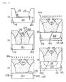
- Fig. 1 (a) shows one example of a bipolar transistor obtainable by a manufacturing method according to the present invention.
- a collector region 2 is formed in the vicinity of the surface of a silicon substrate 1; and a base region 3 is formed on the surface of this collector region 2 so as to be enveloped in the collector region 2.
- An emitter electrode composed of a first polycrystalline silicon film 5 and a second polycrystalline silicon film 11 is formed on the silicon substrate 1 with an insulating film 4 lying there between; and an emitter region 14 is formed in a part where the emitter electrode 15 comes into contact with the silicon substrate 1.
- Fig. 1(b) shows an example that uses an emitter electrode 15 composed of tungsten 16 and polycrystalline silicon.
- the present process can be applied to a bipolar transistor having such a structure as shown in Fig. 1(b), too.
- a bipolar transistor shown in Fig. 1(a) as an example, one example of a process for manufacturing in accordance with the present invention is described in detail.
- n-type dopant is ion-implanted into the surface of a p-type silicon substrate 1 to form a collector region 2 and, then, p-type dopants is ion-implanted into the surface of the collector region 2 to form a base region 3.
- an insulating film 4 is formed over these. Silicon oxide film is in general used for the insulating film 4.
- a HTO (High Temperature Oxide) film is employed for it, and is grown by the LPCVD (Low Pressure Chemical Vapour Deposition) method under circumstances heated up to 800-820 °C or so.
- the film thickness is set to be, for example, 50-100 nm or so.
- a first polycrystalline silicon film 5 is deposited thereon into a thickness of 50-100 nm or so (Fig. 2(b)).
- a resist 6 having an opening is formed (Fig. 2(c)), and using this resist as a mask, a contact hole to reach the base region 3 is formed by means of dry etching. In this state, etching residues 7 may attach onto the inside of the contact hole (Fig. 2(d)).
- ashing and a treatment with a resist-peeling agent are conducted and, then, a cleaning is carried out using hydrofluoric acid or its salt, and followed by rinsing with pure water.
- the resist and the etching residues 7 are removed by these steps.
- anomalous bodies 8 due to the remnant solution of hydrofluoric acid after rinsing may reattach onto the first polycrystalline silicon film 5 and the inside of the contact hole (Fig. 3(a)). While, in conventional techniques, no treatment is performed for these anomalous bodies, a removing treatment with a cleansing agent is carried out in the present process.
- a cleaning with a cleansing agent containing an oxidant and an alkali is essential, and (ii) a cleaning with a cleansing agent containing an oxidant and an acid is performed appropriately.
- a cleaning agent hydrogen peroxide or the like is preferably utilized.
- the alkali include ammonia and the like, and sulfuric acid, hydrochloric acid and the like can be exemplified for typical examples of the acid.
- anomalous bodies 8 are effectively removed. Further, it gives rise of an increase in surface roughness at the bottom section of the contact hole as well as the first polycrystalline silicon film 5, and leads also to the formation of thin films of silicon oxide 9a and 9b thereon (Fig. 3(b)).
- n-type dopants are ion-implanted into the second polycrystalline silicon film 11 (Fig.4 (a)).
- the n-type dopants are diffused into the base region 3 to form an emitter region 14.
- the thin films of silicon oxide 9a and 9b are balled-up, resulting in their disappearance (Fig. 4(b)).
- this is depicted as an interface 12 after balling-up.
- a lamp annealing method such as the RTA (Rapid Thermal Annealing) is preferable. This method allows an emitter region 14 to be formed as designed and also makes the thin films of silicon oxide 9a and 9b ball-up for sure.
- the temperature is set to be preferably at 950 °C or higher and, for example, in a range of 1000-1100 °C, and more preferably in a range of 1000-1050 °C, and the treatment time period is set to be 10-60 seconds, for instance.
- the first polycrystalline silicon film 5 and the second polycrystalline silicon film 11 are shaped into an emitter electrode by selective etching, whereby a bipolar transistor is accomplished (Fig. 4(c)).
- the thin films of silicon oxide 9a and 9b are formed in the step of Fig. 3(b). Since silicon oxide films are higher hydrophilic than polycrystalline silicon, once such films are formed, no remnant solution is left on them, and thus generation of water-marks or anomalous bodies can be suppressed. Consequently, such a problem of generating anomalous bodies as described in Prior Art, referring to Fig. 3(b), does not arise any longer.
- the second polycrystalline silicon film 11 may be converted into a single-crystalline form in the place where the second polycrystalline silicon film 11 comes into contact with the base region 3, and the phenomenon will bring about an increase in emitter resistance and a retard of the dopant diffusion into the base region 3.
- the present process overcomes such a problem with effect. This effect is presumably attributed to fact that the surface roughness at the bottom section of the contact hole increases and a thin film of silicon oxide 9a is formed thereon.
- the single-crystallization in the second polycrystalline silicon film 11 originates from the surface of the single crystal substrate and progresses along.
- an oxide film covers the surface of the silicon substrate that is the initiation origin for growth, so that the growth into single crystals is prevented.
- the growth of single crystal is inhibited not only by covering the initiation origin for growth with an oxide film but also by the reduced smoothness of the surface for growth.
- the oxide film itself is formed through the use of a cleansing agent, so that its thin thickness can be better controlled, and what is more, its film quality can be more uniform, in comparison with those formed by thermal oxidation or natural oxidation in the air. In consequence, it can ball-up certainly, so that it can lower the emitter electrode resistance and regulate the emitter dopant concentrations according to the design, which leads to a stable h FE .
- polycrystalline silicon constituting the emitter electrode is formed in two separate steps for the first polycrystalline silicon film 5 on the insulating film 4 and the second polycrystalline silicon film 11 thereon, it is possible to prevent an insulating film such as a silicon oxide film to be dissolved by a cleansing agent containing hydrofluoric acid or its salt. As a result, the film thinning or proceeding in side etching within the contact hole can be suppressed.
- the present embodiment illustrates application to a bipolar transistor having an emitter electrode composed of polycrystalline silicon as an example, it is to be well-understood that the present invention may be applied to a bipolar transistor having such an electrode structure as shown in Fig. 1(b), in which a high-refractory metal such as tungsten is laid over polycrystalline silicon.
- bipolar transistors each having a structure shown in Fig. 1(a) were fabricated and their performances were evaluated. The steps of a method fabricating these bipolar transistors are described below.
- a collector region 2 was formed by ion-implanting phosphorus into the surface of a silicon substrate 1; a base region 3 was then formed by ion-implanting boron on the surface of the collector region 2; and Following that, an insulating film 4 of silicon oxide was formed over these surfaces.
- the insulating film 4 was grown by the LPCVD method in a circumstance heated up to 800-820 °C or so, and its thickness was selected in a range of 50-100 nm or so.
- a first polycrystalline silicon film 5 was deposited thereon into a thickness of 50-100 nm or so (Fig. 2(b)). On this first polycrystalline silicon film 5, a resist 6 with an opening was then formed (Fig. 2(c)), and using this resist 6 as a mask, a contact hole to reach the base region 3 was formed by means of dry etching.
- ashing and a treatment with a resist-peeling agent were conducted and, then, a cleaning was carried out using hydrofluoric acid or its salt, followed by a rinsing with pure water.
- the resist 6 and the etching residues 7 were removed thereby (Fig.3 (a)).
- the temperature for this treatment is preferably set to be 50-70 °C, and in the present example, it was set 60 °C or so.
- the time period of treatment was 3-5 minutes. After a rinsing with pure water was performed, the substrate was dried (Fig. 3(b)).
- the first polycrystalline silicon film 5 and the second polycrystalline silicon film 11 were shaped into an emitter electrode 15 through selective etching, whereby a bipolar transistor was accomplished (Fig. 4(c)).
- Bipolar transistors obtained in the way described above were taken as Samples 1. Further, in addition to those, other bipolar transistors were fabricated in the similar way as described above, except that a cleaning with the APM was not carried out. These devices obtained in the latter way were taken as Samples 2.
- the current amplification factor h FE for Sample 1 displayed a marked increase as well as a substantially reduced deviation. Moreover, the emitter electrode resistance for Sample 1 showed an excellent value.
- the bipolar transistor prepared in the process of the present invention will demonstrate a little variation in h FE and exhibit a stable device performance (Fig. 9).
- the process according to the present invention can suppress certainly the single-crystallization of polycrystalline silicon that is to constitute an emitter electrode, as well as to prevent the interface oxide film from remaining, when a heat treatment is conducted to diffuse dopants. Therefore, the process according to the present invention can lower the emitter electrode resistance and also regulate the emitter dopant concentrations according to the design, which will provide a stable h FE .
- the process according to the present invention can prevent anomalous bodies such as water-marks to be produced in a cleaning step following the step for dry etching to form an emitter electrode, and thereby the process will achieve an increase in yield as well as an enhancement of device reliability.
Abstract
Description
- The present invention relates to a process for manufacturing a bipolar transistor.
- The structures of bipolar transistors can be classified into two groups; a conventional type and a SST (Super Self-alignment Technology) type. The structure referred to the conventional type is generally made by forming a collector region and a base region in a substrate by the ion implantation technology or the like, and thereafter forming an emitter electrode above it and diffusing thermally dopants from this emitter electrode to form an emitter region in the base region. Referring to Fig. 7, the manufacturing method of a bipolar transistor with a conventional structure is described in detail below.
- First, as shown in Fig. 7(a), n-type dopants are ion-implanted into the surface of a p-
type silicon substrate 1 to form acollector region 2, and p-type dopants are then ion-implanted to form abase region 3 on the surface of thecollector region 2. Over these, sequentially, aninsulating film 4 and a firstpolycrystalline silicon film 5 are grown in this order (Fig. 7(b)). On this firstpolycrystalline silicon film 5, a resist 6 having an opening is formed (Fig. 7(c)), and using this resist as a mask, a contact hole to reach the base region is formed by means of dry etching. In this state, 7 may attach onto the inside of the contact hole (Fig. 7(d)). - Subsequently, ashing and a treatment with a resist-peeling agent are carried out, and then a cleaning using hydrofluoric acid or its salt is carried out, and followed by a rinsing with pure water. Thereby, the resist and the residues from
etching 7 are removed. Hereupon,anomalous bodies 8 derived from the remnant solution of hydrofluoric acid after rinsing may reattach onto the firstpolycrystalline silicon film 5 and the inside of the contact hole (Fig. 8(a)). Next, after a secondpolycrystalline silicon film 11 is grown over the entire surface of the substrate so as to fill up the inside of the contact hole, n-type dopants are ion-implanted into the secondpolycrystalline silicon film 11 and, then, by applying a heat treatment to the whole substrate, the n-type dopants are made to diffuse into thebase region 3 to form anemitter region 14. After that, the firstpolycrystalline silicon film 5 and the secondpolycrystalline silicon film 11 are shaped into anemitter electrode 15 by selective dry etching, whereby a bipolar transistor is accomplished (Fig. 8(b)). - This conventional technique has, however, the following problems, because
anomalous bodies 8 derived from the remnant solution of hydrofluoric acid after rinsing may reattach onto the firstpolycrystalline silicon film 5 and the inside of the contact hole, as shown in Fig. 8(a). First, when the emitter opening section is formed by dry etching, anomalous bodies lying on the first polycrystalline silicon film serve as a mask, and cause etching remnants. Secondly, sinceanomalous bodies 8 happen to remain also on the interface between theemitter electrode 15 and thebase region 3, they lead to incomplete diffusion of emitter dopants, and thus in some cases, the emitter region may fail to be formed as designed or the emitter electrode resistance may become high. - Next, the so-called SST (Super Self-alignment Technology) structure is described below. In the SST structure, an outer base region is formed around an emitter in the manner of self-alignment and connected to a base electrode through a polycrystalline silicon film. It is deferent from the afore-mentioned conventional structure that a polysilicon film for lead of the base is formed on a substrate and a plurality of heat treatments are required to form a base region by thermal diffusion.
- Fig. 5 is a process for manufacturing a bipolar transistor with a SST structure, disclosed in Japanese Patent Application Laid-open No. 6-69225. Firstly, an element
isolation oxide film 504 is formed on an epitaxial substrate, wherein an n+ collector buriedlayer 502 and n- collectorepitaxial layer 503 are formed on a p-type silicon substrate 501. Next, after a boron-dopedbase polysilicon film 505 is grown and then patterned, asilicon oxide film 506 is grown and, in a region where an emitter is to be formed, an opening is formed through thesilicon oxide film 506 and the p+-typebase polysilicon film 505 to expose the n- collector epitaxial layer 503 (Fig. 5(a)). Following that, a silicon oxide film is grown over the entire surface and this oxide film is etched by anisotropic etching such as the RIE (Reactive Ion Etching) to formsidewalls 507 of the silicon oxide film. A heat treatment is then applied thereto in a nitrogen atmosphere to form p+-type outer base diffusion region 508 (Fig. 5(b)). Next, apolysilicon film 509 that is to serve as an emitter electrode is grown under such a condition that loading of polysilicon deposition apparatus at low temperature or while making hydrogen substitution may allow only little natural oxide film to grow on the interface with theepitaxial layer 503, and thenboron 510 is ion-implanted into thispolysilicon film 509. Subsequently, by applying a lamp heating thereto, for example, at 1050 °C for 60 seconds in a nitrogen atmosphere, boron is made to make solid phase diffusion from theemitter polysilicon film 509 to the n-epitaxial layer 503 to form aboron diffusion region 511 that is to serve as an inner base diffusion region (Fig. 5(c)). After that, arsenic 512 is ion-implanted into thepolysilicon film 509 and then, by applying a lamp heating thereto, for example, at 1050 °C for 10 seconds in a nitrogen atmosphere, arsenic is made also to make solid phase diffusion from theemitter polysilicon film 509 to the n-epitaxial layer 503 to form anemitter diffusion region 513 as well as a base diffusion region 511' in the manner of self-alignment (Fig. 5(d)). Theemitter polysilicon film 509 is then shaped into anemitter polysilicon electrode 509 by patterning. Finally, an opening is made for a base contact and ametal electrode 514 is plated over the emitter polysilicon electrode 509' and thepolysilicon electrode 505 for lead of the base and, then, patterned (Fig. 5(e)). The use of the steps of the double diffusion method as described above allows abipolar transistor with a shallow base diffusion region to be obtained, which decreases various parasitic resistances and capacitances. - While, in order to reduce the emitter resistance, the above process employing the double diffusion method prevent any oxide film from growing on the
epitaxial layer 503, but repeated lamp annealing results in the enlargement of crystalline grains in theemitter polysilicon film 509 that is the very source of diffusion. This single-crystallization event makes it hard to control the concentrations of the dopants and the depth in the emitter-base junction section, and thus bringing about deviation in the diffusion profile. - As for a process to overcome such a problem, the publication set forth discloses another process for manufacturing, as shown in Fig. 6. Firstly, following the same steps as a conventional manufacturing process, the fabrication steps proceeds up to the step of forming a P+ diffusion region 103. In the preceding steps, conditions of pretreatment, loading into a deposition furnace and the like are to be regulated so that such an
oxide film 105 as a natural oxide film of a thickness not less than 5 angstroms but not more than 20 angstroms will be formed on the surface that is to become the interface between anepitaxial layer 101 and an emitter polysilicon layer 104 (Fig. 6(a)). Next, keeping theoxide film 105, anemitter polysilicon film 104 is grown over the entire surface of the epitaxial layer 101 (Fig. 6(b)). After that,boron 106 is ion-implanted into this emitter polysilicon film 104 (Fig. 6(c)). By applying a heating in a furnace thereto, for example, at 900 °C for 20 minutes in a nitrogen atmosphere, boron is then made to make solid phase diffusion from theemitter polysilicon film 104 to the n- epitaxial layer to form aboron diffusion region 107, and so as to prevent theemitter polysilicon film 104 from single-crystallizing by the solid phase epitaxial growth. Subsequently, arsenic 108 is ion-implanted into the polysilicon film 104 (Fig. 6(d)). - After that, by applying a heating in a furnace thereto, for example, at 900 °C for 10 minutes in a nitrogen atmosphere, arsenic is made to make solid phase diffusion from the
emitter polysilicon film 104 to the n-epitaxial layer 101 to form anemitter diffusion region 109 as well as abase diffusion region 107 in the manner of self-alignment. Dopants are then activated by a lamp annealing performed, for example, at 1000 °C for 10 seconds in a nitrogen atmosphere. The heat applied thereat converts theoxide film 105 into balled-up oxides 105', by which a low-resistance electric contact between thepolysilicon film 104 and theepitaxial layer 101 will be obtained (Fig. 6(e)). After that, the polysilicon film is patterned and, finally, an opening is made for a base contact and a metal electrode is plated over the emitter polysilicon electrode and the base polysilicon electrode and then patterned. It is described therein that, with such a process employed, excellent controllability of the base-emitter diffusion profile can be achieved. - Nevertheless, this technique has a problem that it is hard to adapt the treatment conditions for shaping the
oxide film 105 on the boundary surface into a form easy to ball up. Although it is described in the publication set forth that theoxide film 105 on the interface can be easily prepared in the thickness suitable for easy balling up by regulating conditions of pretreatment, loading into a deposition furnace to apply and the like, such controls are not always achieved easily. Furthermore, particularly when such a high temperature heat treatment as a lamp heating is applied, it is difficult for such an oxide film to suppress successfully the single-crystallization from the polycrystalline silicon that is to constitute the emitter electrode, and in some cases which causes a lowering and a deviation of the current amplification factor (hFE) and an increase in the emitter - The present invention provides a process for manufacturing a semiconductor device, comprising the steps of:
- forming a collector region of a first conductive type in the vicinity of the surface of a silicon substrate and a base region of a second conductive type to lie on the surface of the collector region;
- forming an insulating film on said silicon substrate;
- forming a contact hole to reach said base region by etching said insulating film selectively;
- cleaning the surface of said insulating film and the inside of said contact hole, using a cleansing agent containing an oxidant and an alkali;
- forming a polycrystalline silicon film over the entire surface so as to fill up said contact hole and thereafter implanting dopants of the first conductive type into said polycrystalline silicon film;
- applying a heat treatment to the whole substrate to diffuse said dopants into said base region and thereby forming an emitter region of the first conductive type; and
- shaping said polycrystalline silicon film into an emitter electrode by selective etching.
-
- According to the present invention, when a heat treatment is conducted to diffuse dopants, the single-crystallization in polycrystalline silicon can be suppressed certainly, and also the remaining of the interface oxide film can be prevented. Hereby this can lower the emitter electrode resistance and regulate the emitter dopant concentrations according to the design, which leads to a stable hFE. In contrast, in conventional techniques, when dopants are diffused into the base region to form an emitter region by heat treatment of the whole substrate, the polycrystalline silicon in the vicinity of the substrate may be often single-crystallized, which gives rise to an increase in emitter resistance and a retard of the dopant diffusion, as mentioned above. The preset invention overcomes such a problem by carrying out a cleaning, using a cleansing agent containing an oxidant and an alkali, so that it can lower the emitter electrode resistance and regulate the emitter dopant concentrations according to the design, whichwill provide a stable hFE. What causes these effects and advantages to be attained are presumably ascribed to the increased roughness of surfaces at the bottom section of the contact hole and at the exposed portion of the surface of single crystal silicon substrate within the opening, and to thin films of silicon oxide formed thereon. The single-crystallization in polycrystalline silicon on the base region surface originates from the surface of the single crystal substrate and progresses along. In conventional techniques, an oxide film covers the surface of the silicon substrate that is the initiation origin for growth, so that the growth in single crystals is prevented. On the other hand, in the present invention, the growth of single crystal is inhibited not only by covering the initiation origin for growth with an oxide film but also by the reduced smoothness of the surface for growth. Further, the oxide film itself is formed through the use of a cleansing agent, so that its thin thickness can be better controlled, and what is more, its film quality can be more uniform, in comparison with those formed by thermal oxidation or natural oxidation in the air. In consequence, it can ball-up certainly, so that it can lower the emitter electrode resistance and regulate the emitter dopant concentrations according to the design, which leads to a stable hFE.
- Further, according to the present invention, there are employed the steps wherein a collector region and a base region are formed within a substrate beforehand and, subsequently, dopants are thermally diffused to form an emitter region by the heat treatment, so that this step requires only one heat treatment. Therefore, this can prevent the single-crystallization of the polycrystalline silicon film that is the source of emitter diffusion. In the afore-mentioned process for forming a SST structure using a double diffusion method, it is required to apply lamp heatings thereto repeatedly so that the single-crystallization in the emitter polysilicon film causes a serious problem. In contrast with this, since the present invention requires the heat treatment only once for the dopant diffusion, this also facilitates to suppress the single-crystallization in the polycrystalline silicon film effectively.
- In addition, the present invention provides a process for manufacturing a semiconductor device; comprising the steps of:
- forming a collector region of a first conductive type in the vicinity of the surface of a silicon substrate and a base region of a second conductive type to lie on the surface of said collector region;
- forming an insulating film and a first polycrystalline silicon film on said silicon substrate in this order;
- forming a contact hole to reach said base region by etching
said insulating film and the first polycrystalline silicon
film selectively:
- cleaning the surface of said first polycrystalline silicon film and the inside of said contact hole, using a cleansing agent containing an oxidant and an alkali;
- forming a second polycrystalline silicon film over the entire surface so as to fill up said contact hole and thereafter implanting dopants of the first conductive type into said first and second polycrystalline silicon films;
- applying aheat treatment to the whole substrate to diffuse said dopants into said base region and thereby forming an emitter region of the first conductive type; and
- shaping said first and second polycrystalline silicon films into an emitter electrode by selective etching.
-
- This invention exhibits the effects described above, that is, as it can suppress the single-crystallization in the polycrystalline silicon and prevent the interface oxide film from remaining, it can thereby lower the emitter electrode resistance and regulate the emitter dopant concentrations according to the design, which will provide a stable hFE, and apart from these, the present invention has further effects and advantages as follows.
- In the present invention, polycrystalline silicon constituting the emitter electrode is formed in two separate steps for the first and the second polycrystalline silicon films. This increases the degree of freedom for choice of the cleansing agent used in cleaning the inside of the contact hole after its formation. When a polycrystalline silicon film is formed in one step, for instance, if, after the opening section for the emitter is formed by etching, a cleaning is conducted using a cleansing agent containing hydrofluoric acid or its salt for the purpose of removing etching residues, an insulating film such as a silicon oxide film may be also dissolved, which leads to the film thinning or proceeding in side etching within the contact hole, and thereby the fabrication of devices as designed may become difficult occasionally. In the present invention, as the first polycrystalline silicon film is formed on the insulating film, such a structure, where the insulating film is covered with the first polycrystalline silicon film, can solve a problem of this sort. Meanwhile, when such a process is employed, the remaining of the cleansing agent is liable to occur on the first polycrystalline silicon film. The surface of the polycrystalline silicon is higher hydrophobic than those of the insulating films such as a silicon oxide film, so that water-marks and anomalous bodies tend to reattach thereto. The present invention may solve this problem specific to the case in which polycrystalline silicon constituting an emitter electrode is formed in two separate steps for a first and a second polycrystalline silicon films. Namely, by cleaning the surface of the first polycrystalline silicon film and the inside of the contact hole using a cleansing agent containing an oxidant and an alkali, the underlying layer, on which the second polycrystalline silicon film is deposited, is made hydrophilic, whereby water-marks and anomalous bodies are prevented from reattaching thereto. As a result, an increase in yield as well as an enhancement of device reliability can be attained.
- Besides, the first conductive type and second conductive type as used in the present invention can take either combination, as long as they represent opposite conductive types, respectively. In other words, the first conductive type and second conductive type may be n-type and p-type, or alternatively, p-type and n-type, respectively.
- In a process for manufacturing a semiconductor device according to the present invention, after forming the foregoing contact hole, cleaning may be first carried out with a cleansing agent containing hydrofluoric acid or its salt, and said cleaning with the cleansing agent containing an oxidizing agent and an alkali is then conducted. This procedure can remove etching residues effectively.
- In this case, after the former cleaning is carried out with a cleansing agent containing hydrofluoric acid or its salt, the latter cleaning may be conducted in such manners as follows.
- (i) A cleaning with a cleaning agent containing an oxidant and an acid is performed, and thereafter the cleaning with the cleansing agent containing the oxidant and the alkali is conducted.
- (ii) The cleaning with the cleansing agent containing the oxidant and the alkali is performed, and thereafter another cleaning with a cleansing agent containing an oxidant and an acid is conducted.
-
-
- Figs. 1(a) and (b) illustrate schematic cross-sectional views of examples of a bipolar transistor obtainable by a manufacturing embodying the present invention.
- Figs. 2(a) to (d) are a series of views explaining steps for forming an opening to reach a base region in a process embodying the present invention.
- Figs. 3(a) and (b) are a couple of views explaining the cleaning step of a process embodying the present invention.
- Figs. 4(a) to (c) are a series of views explaining steps for forming an emitter region and an emitter electrode in a process embodying the present invention.
- Figs. 5(a) to (e) is a series of views explaining a known process for manufacturing a bipolar transistor with a SST structure.
- Figs. 6(a) to (e) are a series of views explaining another known process for manufacturing a bipolar transistor.
- Figs. 7(a) to (d) are a series of views explaining steps for forming an opening to reach a base region in a conventional process for manufacturing a bipolar transistor with conventional structure.
- Figs. 8(a) and (b) are a couple of views explaining the problem in a conventional manufacturing process for manufacturing a bipolar transistor with conventional structure.
- Fig. 9 compares results of evaluation of the current amplification factors for bipolar transistors fabricated in
-
- Fig. 1 (a) shows one example of a bipolar transistor obtainable by a manufacturing method according to the present invention. A
collector region 2 is formed in the vicinity of the surface of asilicon substrate 1; and abase region 3 is formed on the surface of thiscollector region 2 so as to be enveloped in thecollector region 2. An emitter electrode composed of a firstpolycrystalline silicon film 5 and a secondpolycrystalline silicon film 11 is formed on thesilicon substrate 1 with an insulatingfilm 4 lying there between; and anemitter region 14 is formed in a part where theemitter electrode 15 comes into contact with thesilicon substrate 1. Further, Fig. 1(b) shows an example that uses anemitter electrode 15 composed oftungsten 16 and polycrystalline silicon. The present process can be applied to a bipolar transistor having such a structure as shown in Fig. 1(b), too. Hereafter, referring to a bipolar transistor shown in Fig. 1(a) as an example, one example of a process for manufacturing in accordance with the present invention is described in detail. - First, as shown in Fig. 2(a), n-type dopant is ion-implanted into the surface of a p-
type silicon substrate 1 to form acollector region 2 and, then, p-type dopants is ion-implanted into the surface of thecollector region 2 to form abase region 3. Following that, an insulatingfilm 4 is formed over these. Silicon oxide film is in general used for the insulatingfilm 4. In this preferred embodiment, a HTO (High Temperature Oxide) film is employed for it, and is grown by the LPCVD (Low Pressure Chemical Vapour Deposition) method under circumstances heated up to 800-820 °C or so. The film thickness is set to be, for example, 50-100 nm or so. Next, a firstpolycrystalline silicon film 5 is deposited thereon into a thickness of 50-100 nm or so (Fig. 2(b)). - On this first
polycrystalline silicon film 5, a resist 6 having an opening is formed (Fig. 2(c)), and using this resist as a mask, a contact hole to reach thebase region 3 is formed by means of dry etching. In this state,etching residues 7 may attach onto the inside of the contact hole (Fig. 2(d)). - Subsequently, ashing and a treatment with a resist-peeling agent are conducted and, then, a cleaning is carried out using hydrofluoric acid or its salt, and followed by rinsing with pure water. The resist and the
etching residues 7 are removed by these steps. Hereat,anomalous bodies 8 due to the remnant solution of hydrofluoric acid after rinsing may reattach onto the firstpolycrystalline silicon film 5 and the inside of the contact hole (Fig. 3(a)). While, in conventional techniques, no treatment is performed for these anomalous bodies, a removing treatment with a cleansing agent is carried out in the present process. In this cleaning treatment, (i) a cleaning with a cleansing agent containing an oxidant and an alkali is essential, and (ii) a cleaning with a cleansing agent containing an oxidant and an acid is performed appropriately. For an oxidant, hydrogen peroxide or the like is preferably utilized. Further, examples of the alkali include ammonia and the like, and sulfuric acid, hydrochloric acid and the like can be exemplified for typical examples of the acid. - Examples of the specific procedure for this cleaning treatment are listed below:
- (a) APM cleaning;
- (b) SPM cleaning → APM cleaning;
- (c) APM cleaning → HPM cleaning;
- (d) SPM cleaning → APM cleaning → HPM cleaning; wherein
- APM is a cleansing agent composed of ammonia, hydrogen peroxide and water;
- SPM is a cleansing agent composed of sulfuric acid, hydrogen peroxide and water; and
- HPM is a cleansing agent composed of hydrochloric acid, hydrogen peroxide and water.
-
- With this treatment performed,
anomalous bodies 8 are effectively removed. Further, it gives rise of an increase in surface roughness at the bottom section of the contact hole as well as the firstpolycrystalline silicon film 5, and leads also to the formation of thin films ofsilicon oxide - Next, after a second
polycrystalline silicon film 11 is deposited over the entire surface of the substrate so as to fill up the inside of the contact hole, n-type dopants are ion-implanted into the second polycrystalline silicon film 11 (Fig.4 (a)). - After that, by applying a heat treatment to the whole substrate, the n-type dopants are diffused into the
base region 3 to form anemitter region 14. Hereat, the thin films ofsilicon oxide interface 12 after balling-up. For a method of the heat treatment, a lamp annealing method such as the RTA (Rapid Thermal Annealing) is preferable. This method allows anemitter region 14 to be formed as designed and also makes the thin films ofsilicon oxide - After that, the first
polycrystalline silicon film 5 and the secondpolycrystalline silicon film 11 are shaped into an emitter electrode by selective etching, whereby a bipolar transistor is accomplished (Fig. 4(c)). - In the present process, as the cleaning with the cleansing agent containing the oxidant and the alkali is carried out, the thin films of
silicon oxide - Further, in the known techniques, when the heating treatment of Fig. 3(b) is carried out, the second
polycrystalline silicon film 11 may be converted into a single-crystalline form in the place where the secondpolycrystalline silicon film 11 comes into contact with thebase region 3, and the phenomenon will bring about an increase in emitter resistance and a retard of the dopant diffusion into thebase region 3. The present process overcomes such a problem with effect. This effect is presumably attributed to fact that the surface roughness at the bottom section of the contact hole increases and a thin film ofsilicon oxide 9a is formed thereon. The single-crystallization in the secondpolycrystalline silicon film 11 originates from the surface of the single crystal substrate and progresses along. In the known techniques, an oxide film covers the surface of the silicon substrate that is the initiation origin for growth, so that the growth into single crystals is prevented. On the other hand, in the present process, the growth of single crystal is inhibited not only by covering the initiation origin for growth with an oxide film but also by the reduced smoothness of the surface for growth. Furthermore, the oxide film itself is formed through the use of a cleansing agent, so that its thin thickness can be better controlled, and what is more, its film quality can be more uniform, in comparison with those formed by thermal oxidation or natural oxidation in the air. In consequence, it can ball-up certainly, so that it can lower the emitter electrode resistance and regulate the emitter dopant concentrations according to the design, which leads to a stable hFE. - In addition, in the present embodiment, since polycrystalline silicon constituting the emitter electrode is formed in two separate steps for the first
polycrystalline silicon film 5 on the insulatingfilm 4 and the secondpolycrystalline silicon film 11 thereon, it is possible to prevent an insulating film such as a silicon oxide film to be dissolved by a cleansing agent containing hydrofluoric acid or its salt. As a result, the film thinning or proceeding in side etching within the contact hole can be suppressed. - Besides, although the present embodiment illustrates application to a bipolar transistor having an emitter electrode composed of polycrystalline silicon as an example, it is to be well-understood that the present invention may be applied to a bipolar transistor having such an electrode structure as shown in Fig. 1(b), in which a high-refractory metal such as tungsten is laid over polycrystalline silicon.
- In the examples presented hereafter, bipolar transistors each having a structure shown in Fig. 1(a) were fabricated and their performances were evaluated. The steps of a method fabricating these bipolar transistors are described below.
- First, as shown in Fig. 2(a), a
collector region 2 was formed by ion-implanting phosphorus into the surface of asilicon substrate 1; abase region 3 was then formed by ion-implanting boron on the surface of thecollector region 2; and Following that, an insulatingfilm 4 of silicon oxide was formed over these surfaces. The insulatingfilm 4 was grown by the LPCVD method in a circumstance heated up to 800-820 °C or so, and its thickness was selected in a range of 50-100 nm or so. Next, a firstpolycrystalline silicon film 5 was deposited thereon into a thickness of 50-100 nm or so (Fig. 2(b)). On this firstpolycrystalline silicon film 5, a resist 6 with an opening was then formed (Fig. 2(c)), and using this resist 6 as a mask, a contact hole to reach thebase region 3 was formed by means of dry etching. - Subsequently, ashing and a treatment with a resist-peeling agent were conducted and, then, a cleaning was carried out using hydrofluoric acid or its salt, followed by a rinsing with pure water. The resist 6 and the
etching residues 7 were removed thereby (Fig.3 (a)). After that, a cleaning with the APM (ammonia : hydrogen peroxide : water = 1 : 4 : 20 (in volume ratio)) was carried out. The temperature for this treatment is preferably set to be 50-70 °C, and in the present example, it was set 60 °C or so. The time period of treatment was 3-5 minutes. After a rinsing with pure water was performed, the substrate was dried (Fig. 3(b)). - Next, after a second
polycrystalline silicon film 11 was deposited over the entire surface of the substrate so as to fill up the inside of the contact hole, arsenic were ion-implanted into the second polycrystalline silicon film 11 (Fig.4 (a)). - After that, by applying a heat treatment to the whole substrate by means of the RTA, arsenic was diffused into the
base region 3 to form anemitter region 14. The temperature for this treatment was set to be 1025 °C and its time period, 40 seconds (Fig. 4(b)). - Sequentially, the first
polycrystalline silicon film 5 and the secondpolycrystalline silicon film 11 were shaped into anemitter electrode 15 through selective etching, whereby a bipolar transistor was accomplished (Fig. 4(c)). - Bipolar transistors obtained in the way described above were taken as
Samples 1. Further, in addition to those, other bipolar transistors were fabricated in the similar way as described above, except that a cleaning with the APM was not carried out. These devices obtained in the latter way were taken asSamples 2. When the hFE for both the samples were measured, the current amplification factor hFE forSample 1 displayed a marked increase as well as a substantially reduced deviation. Moreover, the emitter electrode resistance forSample 1 showed an excellent value. In short, it is confirmed that the bipolar transistor prepared in the process of the present invention will demonstrate a little variation in hFE and exhibit a stable device performance (Fig. 9). - As explained in detail above, the process according to the present invention can suppress certainly the single-crystallization of polycrystalline silicon that is to constitute an emitter electrode, as well as to prevent the interface oxide film from remaining, when a heat treatment is conducted to diffuse dopants. Therefore, the process according to the present invention can lower the emitter electrode resistance and also regulate the emitter dopant concentrations according to the design, which will provide a stable hFE.
- Further, the process according to the present invention can prevent anomalous bodies such as water-marks to be produced in a cleaning step following the step for dry etching to form an emitter electrode, and thereby the process will achieve an increase in yield as well as an enhancement of device reliability.
Claims (8)
- A process for manufacturing a semiconductor device comprising the steps of:forming a collector region of a first conductive type in the vicinity of the surface of a silicon substrate and a base region of a second conductive type to lie on the surface of the collector region;forming an insulating film on said silicon substrate;forming a contact hole to reach said base region by etching said insulating film selectively;cleaning the surface of said insulating film and the inside of said contact hole, using a cleansing agent containing an oxidant and an alkali;forming a polycrystalline silicon film over the entire surface so as to fill up said contact hole and thereafter implanting dopants of the first conductive type into said polycrystalline silicon film;applying a heat treatment to the whole substrate to diffuse said dopants into said base region and thereby forming an emitter region of the first conductive type; andshaping said polycrystalline silicon film into an emitter electrode by selective etching.
- A process for manufacturing a semiconductor device; comprising the steps of:forming a collector region of a first conductive type in the vicinity of the surface of a silicon substrate and a base region of a second conductive type to lie on the surface of said collector region;forming an insulating film and a first polycrystalline silicon film on said silicon substrate in this order;forming a contact hole to reach said base region by etching said insulating film and the first polycrystalline silicon film selectively:cleaning the surface of said first polycrystalline silicon film and the inside of said contact hole, using a cleansing agent containing an oxidant and an alkali;forming a second polycrystalline silicon film over the entire surface so as to fill up said contact hole and thereafter implanting dopants of the first conductive type into said first and second polycrystalline silicon films;applying aheat treatment to the whole substrate to diffuse said dopants into said base region and thereby forming an emitter region of the first conductive type; andshaping said first and second polycrystalline silicon films into an emitter electrode by selective etching.
- A process for manufacturing a semiconductor device claimed in Claim 1 or 2,
wherein, after forming said contact hole, a cleaning with a cleansing agent containing hydrofluoric acid or its salt is carried out and, then, said cleaning with the cleansing agent containing the oxidant and the alkali is conducted. - A process for manufacturing a semiconductor device claimed in Claim 1 or 2,
wherein, after forming said contact hole, a cleaning with a cleansing agent containing hydrofluoric acid or its salt is carried out and, then, another cleaning with a cleansing agent containing an oxidant and an acid is performed, and thereafter said cleaning with the cleansing agent containing the oxidant and the alkali is conducted. - A process for manufacturing a semiconductor device claimed in Claim 1 or 2,
wherein, after forming said contact hole, a cleaning with a cleansing agent containing hydrofluoric acid or its salt is carried out and, then, said cleaning with the cleansing agent containing the oxidant and the alkali is performed, and thereafter another cleaning with a cleansing agent containing an oxidant and an acid is conducted. - A process for manufacturing a semiconductor device claimed in any one of Claims 1-5,
wherein said cleansing agent containing the oxidant and the alkali comprises hydrogen peroxide, ammonia and water. - A process for manufacturing a semiconductor device claimed in any one of Claims 1-6,
wherein said heat treatment to form said emitter region is carried out by a lamp annealing method. - A semiconductor device manufactured by the process claimed in any one of Claims 1-7.
Applications Claiming Priority (2)
| Application Number | Priority Date | Filing Date | Title |
|---|---|---|---|
| JP2001065055A JP4870873B2 (en) | 2001-03-08 | 2001-03-08 | Manufacturing method of semiconductor device |
| JP2001065055 | 2001-03-08 |
Publications (3)
| Publication Number | Publication Date |
|---|---|
| EP1239513A2 true EP1239513A2 (en) | 2002-09-11 |
| EP1239513A3 EP1239513A3 (en) | 2003-05-28 |
| EP1239513B1 EP1239513B1 (en) | 2011-11-09 |
Family
ID=18923777
Family Applications (1)
| Application Number | Title | Priority Date | Filing Date |
|---|---|---|---|
| EP02251663A Expired - Lifetime EP1239513B1 (en) | 2001-03-08 | 2002-03-08 | Manufacturing method of semiconductor device |
Country Status (3)
| Country | Link |
|---|---|
| US (1) | US6472287B2 (en) |
| EP (1) | EP1239513B1 (en) |
| JP (1) | JP4870873B2 (en) |
Cited By (1)
| Publication number | Priority date | Publication date | Assignee | Title |
|---|---|---|---|---|
| WO2008138881A1 (en) * | 2007-05-14 | 2008-11-20 | Basf Se | Method for removing etching residues from semiconductor components |
Families Citing this family (5)
| Publication number | Priority date | Publication date | Assignee | Title |
|---|---|---|---|---|
| JP2002324861A (en) * | 2001-04-24 | 2002-11-08 | Mitsubishi Electric Corp | Semiconductor device and its manufacturing method |
| US20070045227A1 (en) * | 2005-08-31 | 2007-03-01 | Chih-Ning Wu | Method of stripping photoresist |
| JP2007227775A (en) * | 2006-02-24 | 2007-09-06 | Sanyo Electric Co Ltd | Semiconductor device and its manufacturing method |
| JP2009071181A (en) * | 2007-09-14 | 2009-04-02 | Nec Electronics Corp | Method of manufacturing semiconductor device |
| JP2015191947A (en) * | 2014-03-27 | 2015-11-02 | 旭化成エレクトロニクス株式会社 | Semiconductor device and manufacturing method of the same |
Family Cites Families (17)
| Publication number | Priority date | Publication date | Assignee | Title |
|---|---|---|---|---|
| NL8501769A (en) * | 1984-10-02 | 1986-05-01 | Imec Interuniversitair Micro E | BIPOLAR HIGH-JUNCTION TRANSISTOR AND METHOD FOR THE MANUFACTURE THEREOF. |
| US4797372A (en) * | 1985-11-01 | 1989-01-10 | Texas Instruments Incorporated | Method of making a merge bipolar and complementary metal oxide semiconductor transistor device |
| JPH0628266B2 (en) * | 1986-07-09 | 1994-04-13 | 株式会社日立製作所 | Method for manufacturing semiconductor device |
| US5065208A (en) * | 1987-01-30 | 1991-11-12 | Texas Instruments Incorporated | Integrated bipolar and CMOS transistor with titanium nitride interconnections |
| JP2906416B2 (en) | 1988-09-16 | 1999-06-21 | ソニー株式会社 | Silicon etching method |
| JPH0399440A (en) * | 1989-09-12 | 1991-04-24 | Canon Inc | Semiconductor device and manufacture thereof |
| JPH03246947A (en) * | 1990-02-23 | 1991-11-05 | Sony Corp | Semiconductor device |
| US5238849A (en) * | 1990-08-30 | 1993-08-24 | Nec Corporation | Method of fabricating semiconductor device |
| JPH0521595A (en) * | 1991-07-10 | 1993-01-29 | Sharp Corp | Cleaning method of semiconductor substrate |
| JPH0669225A (en) * | 1992-08-19 | 1994-03-11 | Toshiba Corp | Production of bipolar transistor |
| KR0161378B1 (en) * | 1994-06-13 | 1998-12-01 | 김광호 | Manufacturing method for bipolar junction transistor |
| US6124211A (en) * | 1994-06-14 | 2000-09-26 | Fsi International, Inc. | Cleaning method |
| JPH09306867A (en) * | 1996-05-14 | 1997-11-28 | Toyota Central Res & Dev Lab Inc | Manufacturing semiconductor device |
| JP3651160B2 (en) * | 1997-01-31 | 2005-05-25 | ソニー株式会社 | Manufacturing method of semiconductor device |
| JPH10335341A (en) * | 1997-05-28 | 1998-12-18 | Sony Corp | Method of manufacturing semiconductor device |
| JP3528534B2 (en) * | 1997-09-08 | 2004-05-17 | 信越半導体株式会社 | Cleaning method of silicon wafer |
| FR2805923B1 (en) * | 2000-03-06 | 2002-05-24 | St Microelectronics Sa | PROCESS FOR MANUFACTURING A SELF-ALIGNED DOUBLE-POLYSILICON BIPOLAR TRANSISTOR |
-
2001
- 2001-03-08 JP JP2001065055A patent/JP4870873B2/en not_active Expired - Fee Related
-
2002
- 2002-03-06 US US10/090,626 patent/US6472287B2/en not_active Expired - Lifetime
- 2002-03-08 EP EP02251663A patent/EP1239513B1/en not_active Expired - Lifetime
Non-Patent Citations (1)
| Title |
|---|
| None |
Cited By (1)
| Publication number | Priority date | Publication date | Assignee | Title |
|---|---|---|---|---|
| WO2008138881A1 (en) * | 2007-05-14 | 2008-11-20 | Basf Se | Method for removing etching residues from semiconductor components |
Also Published As
| Publication number | Publication date |
|---|---|
| US6472287B2 (en) | 2002-10-29 |
| US20020127832A1 (en) | 2002-09-12 |
| EP1239513B1 (en) | 2011-11-09 |
| JP2002270813A (en) | 2002-09-20 |
| EP1239513A3 (en) | 2003-05-28 |
| JP4870873B2 (en) | 2012-02-08 |
Similar Documents
| Publication | Publication Date | Title |
|---|---|---|
| JP3600399B2 (en) | Fabrication process for devices with thin layers of cobalt silicide | |
| JP2720793B2 (en) | Method for manufacturing semiconductor device | |
| JPH09283440A (en) | Method for forming selective epitaxial film | |
| KR19980045028A (en) | Silicon / silicon germanium dipole transistor manufacturing method | |
| JPH0955387A (en) | Manufacture of semiconductor integrated circuit device | |
| JPH08293465A (en) | Manufacture of semiconductor device | |
| US6472287B2 (en) | Manufacturing method of semiconductor with a cleansing agent | |
| JP2910382B2 (en) | Method for manufacturing semiconductor device | |
| KR100861739B1 (en) | Thin buried oxides by low-dose oxygen implantation into modified silicon | |
| US5476800A (en) | Method for formation of a buried layer for a semiconductor device | |
| JP2550906B2 (en) | Semiconductor device and manufacturing method thereof | |
| KR100495284B1 (en) | Manufacturing method of semiconductor device | |
| JP2000114515A (en) | Manufacture of semiconductor device | |
| JPS5852843A (en) | Manufacture of semiconductor integrated circuit device | |
| JP2002184783A (en) | Method of manufacturing semiconductor device | |
| JP3104067B2 (en) | Semiconductor device manufacturing method | |
| JPS62133760A (en) | Manufacture of bipolar transistor | |
| JP2793248B2 (en) | Manufacturing method of semiconductor / element structure | |
| JPH0682668B2 (en) | Method for manufacturing semiconductor device | |
| JP2956616B2 (en) | Method for manufacturing semiconductor device | |
| JP3628291B2 (en) | Semiconductor device and manufacturing method of semiconductor device | |
| JPH05251358A (en) | Manufacture of semiconductor device | |
| JP2546650B2 (en) | Method of manufacturing bipolar transistor | |
| JPS60103613A (en) | Manufacture of semiconductor device | |
| JPH01300559A (en) | Manufacture of bipolar semiconductor integrated circuit device |
Legal Events
| Date | Code | Title | Description |
|---|---|---|---|
| PUAI | Public reference made under article 153(3) epc to a published international application that has entered the european phase |
Free format text: ORIGINAL CODE: 0009012 |
|
| AK | Designated contracting states |
Kind code of ref document: A2 Designated state(s): AT BE CH CY DE DK ES FI FR GB GR IE IT LI LU MC NL PT SE TR |
|
| AX | Request for extension of the european patent |
Free format text: AL;LT;LV;MK;RO;SI |
|
| PUAL | Search report despatched |
Free format text: ORIGINAL CODE: 0009013 |
|
| RAP1 | Party data changed (applicant data changed or rights of an application transferred) |
Owner name: NEC ELECTRONICS CORPORATION |
|
| AK | Designated contracting states |
Designated state(s): AT BE CH CY DE DK ES FI FR GB GR IE IT LI LU MC NL PT SE TR |
|
| AX | Request for extension of the european patent |
Extension state: AL LT LV MK RO SI |
|
| 17P | Request for examination filed |
Effective date: 20030922 |
|
| AKX | Designation fees paid |
Designated state(s): GB IT |
|
| REG | Reference to a national code |
Ref country code: DE Ref legal event code: 8566 |
|
| 17Q | First examination report despatched |
Effective date: 20080627 |
|
| RAP1 | Party data changed (applicant data changed or rights of an application transferred) |
Owner name: RENESAS ELECTRONICS CORPORATION |
|
| GRAP | Despatch of communication of intention to grant a patent |
Free format text: ORIGINAL CODE: EPIDOSNIGR1 |
|
| GRAS | Grant fee paid |
Free format text: ORIGINAL CODE: EPIDOSNIGR3 |
|
| GRAA | (expected) grant |
Free format text: ORIGINAL CODE: 0009210 |
|
| AK | Designated contracting states |
Kind code of ref document: B1 Designated state(s): GB IT |
|
| REG | Reference to a national code |
Ref country code: GB Ref legal event code: FG4D |
|
| PLBE | No opposition filed within time limit |
Free format text: ORIGINAL CODE: 0009261 |
|
| STAA | Information on the status of an ep patent application or granted ep patent |
Free format text: STATUS: NO OPPOSITION FILED WITHIN TIME LIMIT |
|
| 26N | No opposition filed |
Effective date: 20120810 |
|
| REG | Reference to a national code |
Ref country code: GB Ref legal event code: 732E Free format text: REGISTERED BETWEEN 20140911 AND 20140917 |
|
| PGFP | Annual fee paid to national office [announced via postgrant information from national office to epo] |
Ref country code: IT Payment date: 20190322 Year of fee payment: 18 |
|
| PGFP | Annual fee paid to national office [announced via postgrant information from national office to epo] |
Ref country code: GB Payment date: 20200327 Year of fee payment: 19 |
|
| PG25 | Lapsed in a contracting state [announced via postgrant information from national office to epo] |
Ref country code: IT Free format text: LAPSE BECAUSE OF NON-PAYMENT OF DUE FEES Effective date: 20200308 |
|
| GBPC | Gb: european patent ceased through non-payment of renewal fee |
Effective date: 20210308 |
|
| PG25 | Lapsed in a contracting state [announced via postgrant information from national office to epo] |
Ref country code: GB Free format text: LAPSE BECAUSE OF NON-PAYMENT OF DUE FEES Effective date: 20210308 |