EP1251365A1 - Microlens array and method of its manufacturing - Google Patents
Microlens array and method of its manufacturing Download PDFInfo
- Publication number
- EP1251365A1 EP1251365A1 EP02008858A EP02008858A EP1251365A1 EP 1251365 A1 EP1251365 A1 EP 1251365A1 EP 02008858 A EP02008858 A EP 02008858A EP 02008858 A EP02008858 A EP 02008858A EP 1251365 A1 EP1251365 A1 EP 1251365A1
- Authority
- EP
- European Patent Office
- Prior art keywords
- microlens array
- holes
- manufacturing
- array according
- substrate
- Prior art date
- Legal status (The legal status is an assumption and is not a legal conclusion. Google has not performed a legal analysis and makes no representation as to the accuracy of the status listed.)
- Granted
Links
- 238000004519 manufacturing process Methods 0.000 title claims abstract description 75
- 238000000034 method Methods 0.000 title description 29
- 239000000463 material Substances 0.000 claims abstract description 131
- 239000000758 substrate Substances 0.000 claims abstract description 88
- 230000003287 optical effect Effects 0.000 claims description 36
- 239000011521 glass Substances 0.000 claims description 29
- 229920005989 resin Polymers 0.000 claims description 16
- 239000011347 resin Substances 0.000 claims description 16
- 230000001070 adhesive effect Effects 0.000 claims description 13
- 239000002131 composite material Substances 0.000 claims description 11
- 239000004033 plastic Substances 0.000 claims description 11
- 229920003023 plastic Polymers 0.000 claims description 11
- 238000003491 array Methods 0.000 claims description 9
- 230000000415 inactivating effect Effects 0.000 claims description 7
- 239000012815 thermoplastic material Substances 0.000 claims description 7
- 229920001296 polysiloxane Polymers 0.000 claims description 6
- 229910010293 ceramic material Inorganic materials 0.000 claims description 5
- 239000002657 fibrous material Substances 0.000 claims description 5
- 229920001187 thermosetting polymer Polymers 0.000 claims description 5
- 238000002347 injection Methods 0.000 claims description 4
- 239000007924 injection Substances 0.000 claims description 4
- 238000010030 laminating Methods 0.000 claims description 4
- 230000008021 deposition Effects 0.000 claims description 2
- 230000001846 repelling effect Effects 0.000 claims description 2
- 238000005342 ion exchange Methods 0.000 description 16
- 238000009736 wetting Methods 0.000 description 16
- 239000007788 liquid Substances 0.000 description 15
- 239000007787 solid Substances 0.000 description 15
- 230000008878 coupling Effects 0.000 description 14
- 238000010168 coupling process Methods 0.000 description 14
- 238000005859 coupling reaction Methods 0.000 description 14
- 239000000853 adhesive Substances 0.000 description 11
- 150000002500 ions Chemical class 0.000 description 10
- 239000012528 membrane Substances 0.000 description 10
- 238000009792 diffusion process Methods 0.000 description 9
- 239000002184 metal Substances 0.000 description 7
- 229910052751 metal Inorganic materials 0.000 description 7
- 239000002019 doping agent Substances 0.000 description 6
- 239000004840 adhesive resin Substances 0.000 description 5
- 229920006223 adhesive resin Polymers 0.000 description 5
- 230000015572 biosynthetic process Effects 0.000 description 5
- 230000008859 change Effects 0.000 description 5
- 239000013307 optical fiber Substances 0.000 description 5
- 230000008569 process Effects 0.000 description 5
- 238000004891 communication Methods 0.000 description 4
- 238000004806 packaging method and process Methods 0.000 description 4
- 239000000835 fiber Substances 0.000 description 3
- 150000002739 metals Chemical class 0.000 description 3
- 150000003839 salts Chemical class 0.000 description 3
- 125000006850 spacer group Chemical group 0.000 description 3
- 229920000049 Carbon (fiber) Polymers 0.000 description 2
- 239000004593 Epoxy Substances 0.000 description 2
- 239000004917 carbon fiber Substances 0.000 description 2
- 239000000919 ceramic Substances 0.000 description 2
- 238000000576 coating method Methods 0.000 description 2
- 238000007796 conventional method Methods 0.000 description 2
- 238000001816 cooling Methods 0.000 description 2
- 238000001723 curing Methods 0.000 description 2
- 238000010894 electron beam technology Methods 0.000 description 2
- 239000011152 fibreglass Substances 0.000 description 2
- 238000010438 heat treatment Methods 0.000 description 2
- 230000002779 inactivation Effects 0.000 description 2
- VNWKTOKETHGBQD-UHFFFAOYSA-N methane Chemical compound C VNWKTOKETHGBQD-UHFFFAOYSA-N 0.000 description 2
- 238000005268 plasma chemical vapour deposition Methods 0.000 description 2
- XLYOFNOQVPJJNP-UHFFFAOYSA-N water Substances O XLYOFNOQVPJJNP-UHFFFAOYSA-N 0.000 description 2
- LFQSCWFLJHTTHZ-UHFFFAOYSA-N Ethanol Chemical compound CCO LFQSCWFLJHTTHZ-UHFFFAOYSA-N 0.000 description 1
- 229920002430 Fibre-reinforced plastic Polymers 0.000 description 1
- 241000238631 Hexapoda Species 0.000 description 1
- 239000011157 advanced composite material Substances 0.000 description 1
- 230000004075 alteration Effects 0.000 description 1
- 229910003481 amorphous carbon Inorganic materials 0.000 description 1
- 238000007743 anodising Methods 0.000 description 1
- 229920006231 aramid fiber Polymers 0.000 description 1
- 230000001174 ascending effect Effects 0.000 description 1
- 230000005540 biological transmission Effects 0.000 description 1
- 238000006243 chemical reaction Methods 0.000 description 1
- 239000003795 chemical substances by application Substances 0.000 description 1
- 239000011248 coating agent Substances 0.000 description 1
- 150000001875 compounds Chemical class 0.000 description 1
- 238000005520 cutting process Methods 0.000 description 1
- 238000000151 deposition Methods 0.000 description 1
- 238000009826 distribution Methods 0.000 description 1
- 230000002708 enhancing effect Effects 0.000 description 1
- 238000005530 etching Methods 0.000 description 1
- 239000011151 fibre-reinforced plastic Substances 0.000 description 1
- 239000013305 flexible fiber Substances 0.000 description 1
- 229920002457 flexible plastic Polymers 0.000 description 1
- 238000013007 heat curing Methods 0.000 description 1
- 230000002209 hydrophobic effect Effects 0.000 description 1
- 230000010365 information processing Effects 0.000 description 1
- 239000012784 inorganic fiber Substances 0.000 description 1
- 238000010884 ion-beam technique Methods 0.000 description 1
- 230000001678 irradiating effect Effects 0.000 description 1
- 238000010329 laser etching Methods 0.000 description 1
- 229910052745 lead Inorganic materials 0.000 description 1
- 239000004973 liquid crystal related substance Substances 0.000 description 1
- 239000008204 material by function Substances 0.000 description 1
- 239000011159 matrix material Substances 0.000 description 1
- 238000007747 plating Methods 0.000 description 1
- 230000009467 reduction Effects 0.000 description 1
- 239000012779 reinforcing material Substances 0.000 description 1
- 239000004065 semiconductor Substances 0.000 description 1
- 238000007493 shaping process Methods 0.000 description 1
- 238000004904 shortening Methods 0.000 description 1
- 229910052709 silver Inorganic materials 0.000 description 1
- 238000004544 sputter deposition Methods 0.000 description 1
- 238000004381 surface treatment Methods 0.000 description 1
- 229910052716 thallium Inorganic materials 0.000 description 1
Images


Classifications
-
- G—PHYSICS
- G02—OPTICS
- G02B—OPTICAL ELEMENTS, SYSTEMS OR APPARATUS
- G02B3/00—Simple or compound lenses
- G02B3/0006—Arrays
- G02B3/0037—Arrays characterized by the distribution or form of lenses
- G02B3/0056—Arrays characterized by the distribution or form of lenses arranged along two different directions in a plane, e.g. honeycomb arrangement of lenses
-
- B—PERFORMING OPERATIONS; TRANSPORTING
- B29—WORKING OF PLASTICS; WORKING OF SUBSTANCES IN A PLASTIC STATE IN GENERAL
- B29D—PRODUCING PARTICULAR ARTICLES FROM PLASTICS OR FROM SUBSTANCES IN A PLASTIC STATE
- B29D11/00—Producing optical elements, e.g. lenses or prisms
- B29D11/00009—Production of simple or compound lenses
- B29D11/00365—Production of microlenses
- B29D11/00375—Production of microlenses by moulding lenses in holes through a substrate
-
- G—PHYSICS
- G02—OPTICS
- G02B—OPTICAL ELEMENTS, SYSTEMS OR APPARATUS
- G02B3/00—Simple or compound lenses
- G02B3/0006—Arrays
- G02B3/0012—Arrays characterised by the manufacturing method
- G02B3/0018—Reflow, i.e. characterized by the step of melting microstructures to form curved surfaces, e.g. manufacturing of moulds and surfaces for transfer etching
-
- G—PHYSICS
- G02—OPTICS
- G02B—OPTICAL ELEMENTS, SYSTEMS OR APPARATUS
- G02B3/00—Simple or compound lenses
- G02B3/0006—Arrays
- G02B3/0037—Arrays characterized by the distribution or form of lenses
- G02B3/0062—Stacked lens arrays, i.e. refractive surfaces arranged in at least two planes, without structurally separate optical elements in-between
- G02B3/0068—Stacked lens arrays, i.e. refractive surfaces arranged in at least two planes, without structurally separate optical elements in-between arranged in a single integral body or plate, e.g. laminates or hybrid structures with other optical elements
-
- H—ELECTRICITY
- H01—ELECTRIC ELEMENTS
- H01L—SEMICONDUCTOR DEVICES NOT COVERED BY CLASS H10
- H01L27/00—Devices consisting of a plurality of semiconductor or other solid-state components formed in or on a common substrate
- H01L27/14—Devices consisting of a plurality of semiconductor or other solid-state components formed in or on a common substrate including semiconductor components sensitive to infrared radiation, light, electromagnetic radiation of shorter wavelength or corpuscular radiation and specially adapted either for the conversion of the energy of such radiation into electrical energy or for the control of electrical energy by such radiation
- H01L27/144—Devices controlled by radiation
- H01L27/146—Imager structures
- H01L27/14601—Structural or functional details thereof
- H01L27/14625—Optical elements or arrangements associated with the device
- H01L27/14627—Microlenses
-
- H—ELECTRICITY
- H01—ELECTRIC ELEMENTS
- H01L—SEMICONDUCTOR DEVICES NOT COVERED BY CLASS H10
- H01L27/00—Devices consisting of a plurality of semiconductor or other solid-state components formed in or on a common substrate
- H01L27/14—Devices consisting of a plurality of semiconductor or other solid-state components formed in or on a common substrate including semiconductor components sensitive to infrared radiation, light, electromagnetic radiation of shorter wavelength or corpuscular radiation and specially adapted either for the conversion of the energy of such radiation into electrical energy or for the control of electrical energy by such radiation
- H01L27/144—Devices controlled by radiation
- H01L27/146—Imager structures
- H01L27/14683—Processes or apparatus peculiar to the manufacture or treatment of these devices or parts thereof
- H01L27/14685—Process for coatings or optical elements
Definitions
- the present invention relates to a microlens array typically used in the fields of optical communication and optical packaging for coupling light emitted from a light source to an optical fiber or an optical waveguide, converting light emitted from the optical fiber or the optical waveguide into parallel rays or so focusing light beams to enter the optical fiber or the optical waveguide in an optical coupling system.
- the microlens in general represents a fine lens having a lens diameter of not more than a several millimeters.
- Various methods relating to the microlens array including methods for manufacturing the same have been proposed in the art.
- the ion exchange diffusion method is widely known as a method for manufacturing the microlens array. In the ion exchange diffusion method, a dopant ion is selectively diffused on a multicomponent glass substrate.
- an ion exchange control membrane 102 is firstly formed on a surface of a multicomponent glass substrate 101 containing a monovalent ion.
- the ion exchange control membrane 102 may be a metal membrane or a dielectric membrane.
- an array of circular apertures 103 at a predetermined pitch that is equivalent to that of an LD array or a PD array is formed on the ion exchange control membrane 102 using a photolithographic technique or a etching technique.
- the diameter of a lens prepared according to this method is determined by each of the apertures 103, and the apertures function as light-shielding membrans for reducing crosstalk between adjacent channels.
- the dopant ion may include Tl, Ag and Pb, each having a high degree of refractive index.
- the glass substrate 101 that is coated with the ion exchange control membrane 102 having the circular apertures 103 is immersed in the molten salt 104 so that the dopant ion is selectively diffused on the glass substrate 101 through the apertures 103 on the ion exchange control membrane 102 to thereby form ion exchange areas 105 each having a hemispheric diffusion front.
- the ion exchange areas 105 serve as distributed refraction type lenses according to a dopant ion distribution.
- the surface of the substrate 101 is expanded according to the volumetric difference between the ions to form convex lenses 106 shown in Fig. 14C.
- a diameter of each of the convex lenses 106 is typically in a range of from a several tens of microns to a several hundreds of microns.
- the above-illustrated ion exchange diffusion method is suitable for forming a microlens having a diameter of from a several tens of microns to a several hundreds of microns; however, problems have been found with the method in manufacture of a microlens having a relatively large lens diameter or a lens effective diameter of from a several hundreds of microns to a several millimeters. More specifically, in order to prepare the relatively large microlens employing the ion exchange diffusion method, a depth of the diffusion must be a several hundreds of microns or more that is about the same as the size of the lens to be produced and it is necessary to conduct a heat treatment at a high temperature for a remarkably long time.
- an object of the present invention is to provide a method of manufacturing a microlens array that realizes downsized and high-performance optical coupling elements to be used in the fields of optical communication and optical packaging.
- the 1st invention of the present invention is a method of manufacturing a microlens array comprising forming microlenses by dropping or injecting to a plurality of through holes formed on a substrate a liquefied lens material so as to dispose the lens material at each of the through holes, the lens material being curable and has a predetermined transmittivity and a predetermined viscosity.
- the 2nd invention of the present invention is the method of manufacturing a microlens array according to 1st invention, wherein a curvature of each of the microlens is varied by adjusting whole or part of (1) configurations or sizes of the through holes of the substrate,(2) wettability between the substrate and the lens material, (3)a viscosity of the lens material and (4)a quantity of lens material in a droplet or in an injection shot.
- the 3rd invention of the present invention is the method of manufacturing a microlens array according to 1st invention, wherein the lens material is dropped or injected substantially simultaneously by using nozzles that can drop or inject the lens material substantially simultaneously to the through holes.
- the 4th invention of the present invention is the method of manufacturing a microlens array according to 1st invention, wherein the lens material is a ultraviolet ray curable resin material, a thermosetting resin material, a thermoplastic material or a glass material.
- the 5th invention of the present invention is the method of manufacturing a microlens array according to 1st invention, wherein each of the through holes has a truncated conical shape or a step portion.
- the 6th invention of the present invention is the method of manufacturing a microlens array according to 1st invention, wherein the microlenses are convex lenses.
- the 7th invention of the present invention is the method of manufacturing a microlens array according to 1st invention, wherein the microlenses are concave lenses.
- the 8th invention of the present invention is the method of manufacturing a microlens array according to 1st invention, wherein all refractive indexes and/or a transmittivities of the lens materials to be dropped or injected to the plurality of through holes are not same.
- the 9th invention of the present invention is the method of manufacturing a microlens array according to 1st invention, wherein a whole or a part of the plurality of through holes vary in size, and the lens material is dropped or injected in accordance with the sizes of the through holes.
- the 10th invention of the present invention is the method of manufacturing a microlens array according to 1st invention, wherein the plurality of through holes are arranged on the substrate to give a closest packed structure, each of the through holes having the shape of a hexagon of a predetermined size.
- the 11th invention of the present invention is the method of manufacturing a microlens array according to 1st invention, wherein the substrate is formed from silicone, a plastic material, a glass material, ceramic material, fiber material or a composite material.
- the 12th invention of the present invention is a microlens multilayer formed by laminating a plurality of microlens arrays produced by the method of manufacturing a microlens array according to any one of 1st to 11th inventions, wherein the plurality of microlens arrays are so laminated that optical axes of the microlenses of each microlens array coincide with the optical axes of the corresponding microlenses of another microlens array.
- the 13th invention of the present invention is a microlens array comprising a substrate in which a plurality of through holes are formed and a plurality of microlenses respectively disposed at the through holes in the substrate, wherein
- the microlenses are fixed to the through holes of the substrate by way of adhesion or deposition of a microlens material to a substrate material.
- the 14th invention of the present invention is the microlens array according to 13th invention, wherein the microlenses are formed of a ultraviolet ray curable resin material, a thermosetting resin material, a thermoplastic material or a glass material.
- the 15th invention of the present invention is the method of manufacturing a microlens array according to 13th invention, wherein each of the through holes has a truncated conical shape or a step portion.
- the 16th invention of the present invention is the method of manufacturing a microlens array according to 13th invention, wherein the microlenses are convex lenses.
- the 17th invention of the present invention is the method of manufacturing a microlens array according to 13th invention, wherein the microlenses are concave lenses.
- the 18th invention of the present invention is the method of manufacturing a microlens array according to 13th invention, wherein all refractive indexes and/or a transmittivities of the lens material to be dropped or injected to the plurality of through holes are not same.
- the 19th invention of the present invention is the method of manufacturing a microlens array according to 13th invention, wherein a whole or a part of the plurality of through holes vary in size and a whole or a part of the microlenses vary in size in accordance with the sizes of the through holes.
- the 20th invention of the present invention is the method of manufacturing a microlens array according to 13th invention, wherein the plurality of through holes are arranged in the substrate to give a closest packed structure, each of the through holes having the shape of a hexagon of a predetermined size.
- the 21st invention of the present invention is the method of manufacturing a microlens array according to 13th invention, wherein the substrate is formed of any one of silicone, a thermoplastic material, a glass material, a ceramic material, a fiber material and a composite material.
- the 22nd invention of the present invention is the method of manufacturing a microlens array according to 1st invention, wherein each of the microlenses has a multilayer structure that consists of a plurality of layers varying in material and refractive index.
- the 23rd invention of the present invention is the method of manufacturing a microlens array according to 1st invention, wherein each of the plurality of through holes in the substrate has a rectangular shape of a predetermined size and each of the microlenses that is formed by dropping has an anamorphotic or cylindrical configuration.
- the 24th invention of the present invention is the method of manufacturing a microlens array according to 1st invention, comprising subjecting a surface of the substrate to an inactivating treatment so that a portion of the surface excluding the through holes has repelling properties to the lens material and the through holes have adhesive properties to the lens material.
- the 25th invention of the present invention is the method of manufacturing a microlens array according to 24th invention, wherein the surface of the substrate is caused to be uneven by the inactivating treatment.
- Fig. 1 is a perspective view showing a microlens array according to a first embodiment of the present invention.
- the microlens array in the first embodiment comprises a substrate 11 in which a plurality of through holes are provided and convex lenses 12 arranged on each of the through holes in the substrate 11, wherein a diameter of each of the convex lenses is from about a several tens of microns to about a several millimeters.
- the convex lenses 12 have light transmitting properties and they are formed from a curable liquefied resin material or a thermoplastic material or a glass material that can be cured on the substrate 11.
- Fig. 2 is a cross-sectional view of the microlens array according to the first embodiment of the present invention described above with reference to Fig. 1, showing a state wherein the convex lenses are respectively disposed at the through holes on the substrate 11.
- the microlens array according to the first embodiment is characterized in that a lens material, which is the resin material or the heated and liquefied plastic material or glass material described above, is dropped or injected to the through holes formed on the substrate 11 and that the convex lenses are disposed by taking advantages of a surface tension of the lens material. Further, positions of the convex lenses can be set arbitrarily depending on positions of the through holes disposed on the substrate 11.
- the positioning of the convex lenses 12 on the substrate 11 is facilitated by dropping or injecting the lens material to the through holes after forming the through holes on the substrate 11.
- the positions and sizes of the though holes can be defined arbitrarily by employing a fine processing technique according to the substrate material and, therefore, it is possible to form the through holes with a remarkably high degree of precision.
- it is possible to control optical characteristics of the lenses by properly selecting the refractive index of the lens material.
- it is possible to control a curvature of each of the lenses by adjusting a viscosity of the lens material before curing and an amount of drop or injection of the lens material to each of the through holes.
- the microlens array according to the first embodiment of the present invention is characterized in that the positions and the optical characteristics of the lenses are controlled simultaneously and with a remarkably high degree of precision. Further, it is possible to form lenses of a wide range of effective diameters of from about a several tens of microns to about a several millimeters by adjusting a wettability, a viscosity and an amount of drop of the lens material to the substrate material.
- the microlens array according to the first embodiment of the present invention is remarkably advantageous in terms of the optical coupling since the focal length is about the same as that of the diameter of each of the lenses and both surfaces of the lens are open to air without contacting the substrate material.
- the material used for forming the substrate 11 of the microlens array according to the first embodiment of the present invention is not necessarily an optical material having light transmitting properties such as the plastic material or the glass material. More specifically, it is possible to form the microlens array if the substrate 11 is not formed from the optical material. In the case where the substrate 11 is formed from a material other than the optical material, the substrate 11 functions as an optical mask for the lenses to be formed on the substrate, thereby preventing stray lights from entering the lenses, which is remarkably effective in practical use.
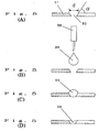
- Figs. 3A to 3E are illustrations for a method of manufacturing microlens array according to a second embodiment of the present invention.
- the method of manufacturing microlens array of the second embodiment in the case of using a glass material for a substrate 31 and an adhesive resin material having light transmitting properties as a material for lenses 35 as shown in Figs. 3A to 3E will be described in detail below.
- through holes 32 are formed on a substrate 31 precisely by employing various fine processing techniques.
- the fine processing techniques to be employed may be an ultraprecise cutting, a laser processing, a focusing ion beam processing, a laser etching, a microdischarging, an electron beam writing.
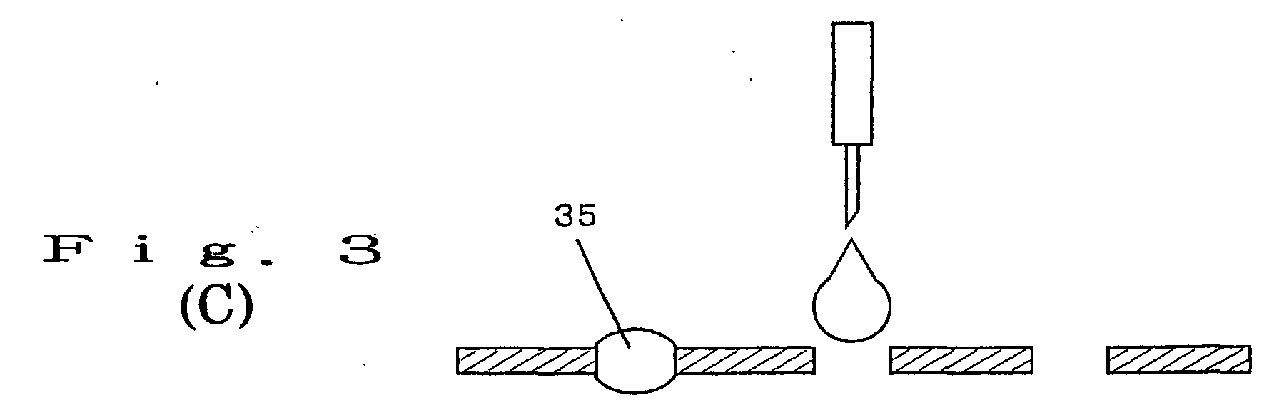
- an adhesive material 34 is dropped from drop nozzles 33.
- a viscosity of the adhesive material 34 is so selected that the adhesive material stays in the through holes 32 without falling therefrom as shown in Fig. 3C.
- the viscosity and dropping amount must be selected properly to prevent the lens material 34 from falling from the through holes 32.
- the adhesive resin material 34 which is the lens material, is dropped sequentially to the through holes disposed on the substrate as shown in Fig. 3D.
- the dropped adhesive resin material is then subjected to a heat curing or a ultraviolet ray curing method depending on characteristics of the resin to form convex lenses, thereby completing the production of microlens array shown in Fig. 3E.
- Epoxy-based adhesive resins or the like having light transmitting properties may be used as a thermosetting resin, while fluoridated epoxy-based resins or the like may be used as a ultraviolet ray curable resin.
- FIG. 4A to 4C A method of manufacturing microlens array according to a third embodiment of the present invention that is illustrated in Figs. 4A to 4C will be described below.
- the process illustrated in Figs. 4A to 4C is different from that illustrated in Figs. 3A to 3E by a nozzle unit 44 that is formed by integrating a plurality of nozzles in order to shorten a time required for the production.
- a microlens array comprising the plurality of convex lenses can be two-dimensionally produced in a remarkably short period and effectively.
- FIG. 5A to 5D A method of manufacturing microlens array according to a fourth embodiment of the present invention that is illustrated in Figs. 5A to 5D will be described below.
- the process illustrated in Figs. 5A to 5D is different from that illustrated in Figs. 4A to 4C in a tapered through hole 52 that is formed on a substrate 52. That is, the through hole has a truncated conical shape.
- the tapering of the through hole 52 makes it possible to control a curvature of a lens surface of a convex lens 55 that is formed on the through hole 52 by dropping a lens material 34 from a nozzle 33.
- Figs. 5A to 5D it is possible to change the curvature of the lens by changing a configuration of the through hole.
- wet means that the liquid spreads over the solid to cover its surface and "do not wet” means that the liquid does not spread but forms a spherical surface.
- the phenomenon of wetting varies considerably depending on properties of the surface of the solid and properties of the liquid.
- Equation 1 ⁇ S is a surface tension of the solid, ⁇ SL is a surface tension of the liquid, ⁇ L is an interfacial tension, and ⁇ is a contact angle.
- Figs. 6B to 6D respectively show convex lenses formed on through holes, convex lenses formed on truncated conical through holes and concaved lenses formed on through holes.
- a volume of each of the through holes of Figs. 6B to 6D is indicated by Vb, Vc and Vd;
- a volume of the lens material dropped or injected to each of the through holes is indicated by Lb, Lc and Ld;
- the contact angles of Figs. 6B to 6D are respectively indicated by ⁇ B , ⁇ C and ⁇ D .
- the spread wetting occurs when water is dropped on a clean glass surface; however, it is possible to cause the adhesive wetting on the glass surface by subjecting the surface to a hydrophobication by using a cationic-activating agent.
- a change in a free energy ⁇ G with respect to each of the wettings is obtained by subtracting an interfacial energy that is lost by each of the wettings from an interfacial energy caused by each of the wettings.
- the change in a free energy ⁇ G with respect to the adhesive wetting is represented by the following Equation.
- Equation 7 Equation 7
- Equation 7 the change in free energy with respect to the adhesive wetting can be represented as a coefficient for the surface tension of the liquid and a contact angle ⁇ and it is possible to cause the adhesive wetting when ⁇ G is a positive integer. Accordingly, the adhesive wetting can occur irrespective of ⁇ . However, a reduction in the free energy is relatively large and the wetting tends to occur if a value of ⁇ is relatively small.
- a silicone substrate a ceramic material, a plastic material, a fiber reinforced plastic, a fiber material such as a carbon fiber or a composite material composed of the above materials
- the fiber composite material include a glass fiber reinforced plastic (GFRP) that has widely been used.
- GFRP glass fiber reinforced plastic
- ACM advanced composite material
- ACM A composite material obtainable by combining high-performance and high-functional materials is called "advanced composite material" (ACM)
- ACM A composite material obtainable by combining high-performance and high-functional materials
- ACM advanced composite material
- it is possible to use as the substrate material an ACM comprising a reinforcing material such as a high-performance carbon fiber, an aramid fiber and like inorganic fibers and a whisker as well as a matrix such as various high-performance resins, metals and ceramics.
- a microlens array employing the production method described with reference to Figs. 3A to 3E using a substrate 71 on which hexagon-shaped through holes 72 are formed as shown in Fig. 8, the substrate being formed from a flexible fiber material.
- a flexible microlens sheet as a lens material to fill the through holes 72 to form lenses 73 by using a flexible resin material or a flexible plastic material having light-transmitting properties.
- a compound eye similar to that of an insect which has a curved surface
- image recognition device by so forming subminiature CCD elements that the CCD elements respectively correspond to the microlenses formed on the flexible microlens sheet.
- FIG. 9A shows a state wherein two microlens arrays, on which the convex lenses are formed as described above, are laminated in such a manner that their back faces contact to each other and their optical axes coincide with each other.
- Figs. 10A to 10D show production patterns of microlens array according to an eighth embodiment of the present invention.
- Fig. 10A shows a pattern wherein microlenses 92 that are identical in size are formed on a substrate 91 at a same pitch and a constant interval.
- the patterns are applicable to 1 ⁇ N array lenses and N ⁇ N array lenses for the use as an optical interconnection for a parallel optical fiber transmission between chips, modules, boards and the like. Therefore, although the microlenses are typically formed at a pitch of 125 microns or 250 microns, it is possible to form the through holes at an arbitrary pitch.
- microlenses 93 and large diameter microlenses 94 for the use as an incident beam array whose light source or incident light has a sporadic beamform.
- the microlenses of arbitrary sizes that vary in diameter can be used in combination by adjusting processing sizes of the through holes to be formed on the substrate 91.
- a lens array As shown in Fig. 10C, it is also possible to produce a lens array by shortening an interval between a microlens 94 and an adjacent microlens 95. Further, as shown in Fig. 10D, it is possible to dispose microlenses in the manner of fine fill disposition as shown in Fig. 8 by moving microlenses 96 of a first array and microlenses 97 of a second array. It is possible to further improve characteristics of the microlens array by forming a lens array by the use of a several types of lenses in combination in accordance with the properties of the light source and incident beam, the several types of lenses being those formed of lens materials that vary in optical properties i.e. refractive index and wavelength transmitting properties or those of different sizes.
- FIG. 11A A manufacturing method of microlens array according to a ninth embodiment of the present invention will be described with reference to Figs. 11A to 11C.
- the process illustrated in Figs. 11A to 11C is different from that illustrated in Figs. 4A to 4C in lenses to be formed, i.e., composite lenses that vary in refractive index are formed in the process of Figs. 11A to 11C.
- a plurality of spherical microlens arrays 111 is formed two-dimensionally as shown in Fig. 11A, and then the microlens array substrate is reversed as shown in Fig. 11B. After that, the composite lenses are formed by dropping the materials 113 that vary in refractive index as shown in Fig. 11C.
- the microlens array of composite refractive index by using the materials that vary in refractive index in combination. Accordingly, the lenses formed from the materials varying in refractive index function as achromatic lenses, thereby realizing microlenses capable of reducing chromatic aberration.
- FIG. 12A and 12B A manufacturing method of microlens array according to a tenth embodiment of the present invention will be described with reference to Figs. 12A and 12B.
- the process illustrated in Figs. 12A and 12B is different from that illustrated in Figs. 5A to 5D in through holes, i.e., as shown in Fig 12A, each of through holes 122 has a rectangular shape and long sides of each of the through holes 122 have tapering 123. Since the through holes have the rectangular shape and long sides thereof are tapered as described above, convex lenses formed on the through holes by dropping a lens material each having an oval curvature as lenses 124 shown in Fig. 12B.
- the oval lenses 124 thus formed function as anamorphotic lenses and capable of shaping a beam that is emitted from a semiconductor laser and asymmetric in lengthwise and crosswise to be symmetric, thereby enhancing coupling efficiency with an optical fiber or a light reception element to a remarkably high degree.
- the anamorphotic lenses are shown in Fig. 12B, it is possible to form cylindrical lenses by modifying the shapes of through holes.
- FIG. 13A and 13B A manufacturing method of microlens array according to an eleventh embodiment of the present invention will be described with reference to Figs. 13A and 13B.
- the method illustrated in Figs. 13A and 13B is different from that illustrated in Figs. 5A to 5D in a substrate structure, i.e., the substrate structure shown in Figs. 13A and 13b is a three layer structure formed by subjecting a surface of a solid substrate 134 that is relatively low in solid-liquid interfacial energy to an inactivating treatment to cause the adhesive wetting.
- the three layer structure achieved by the inactivating treatment of the surface 133 a portion of the surface 133 at which through holes are not formed repels a lens material 135 to thereby contribute to fixing the lens material 135 in the through holes.
- Examples of the inactivating treatment include a method of increasing roughness by irradiating a solid surface with an electron beam and a method of coatings a solid surface for inactivation.
- Other effective treatment may be sputtering, plasma CVD method, eximer laser irradiation, formation of a coating that is highly hydrophobic, formation of an oxide membrane with respect to metals, anodizing method with respect to metals, formation of fluoridated amorphous carbon membrane by the plasma CVD method, plating and the like.
- the smooth surface may be subjected to a roughing treatment to increase the contact angle. Accordingly, it is also possible to increase the adhesive wetting properties by forming fine convexoconcaves of a several microns or less on the smooth surface by a metal pattern processing, etc., thereby simplifying a formation of spherical lenses 135 on the through holes.
- the substrate to be used for the above embodiments is not limited to the glass substrate, and a monocrystal silicone substrate, a ceramic substrate, a plastic substrate, a fiber substrate, a metal substrate or a composite substrate can be used depending on the lens material to be used. It is apparent that the microlens array is obtainable by using any one of the above substrates provided that the method for forming the through holes and the lens material are properly selected.
- the size of the microlens of the present invention depending on the size of each of through holes to be formed on the substrate, and it is possible to produce the microlenses of a wide range of sizes each of which has a diameter from a several tens of microns to a several millimeters. It is possible to control optical properties of the microlens array by way of the lens material to be dropped or injected to the substrate, and each of the microlenses thus obtained is remarkably advantageous in terms of the optical coupling since both surfaces of each of the lenses are open to air without contacting the substrate material.
- the usage of the microlens array of the present invention is not limited to the optical communication elements, and it is possible to apply the microlens array to the optical packaging substrates and also, widely to image information processing devices and liquid crystal display devices, for the optical coupling, optical signal processing, light beam conversion and the like.
- the present invention provides the microlens array that realizes downsized and high-performance optical coupling elements to be used in the fields of the optical communication, the optical packaging and the like and the method of manufacturing the same.
- the present invention it is possible to produce a microlens array of a wide range of lens diameters remarkably easily. Also, according to the present invention, the lenses are disposed at arbitrary positions with both surfaces of each of the lenses being open to air without contacting the substrate material and they are remarkably high in precision. Thus, the present invention realizes the downsized and high-performance optical coupling elements.
Abstract


Description
- The present invention relates to a microlens array typically used in the fields of optical communication and optical packaging for coupling light emitted from a light source to an optical fiber or an optical waveguide, converting light emitted from the optical fiber or the optical waveguide into parallel rays or so focusing light beams to enter the optical fiber or the optical waveguide in an optical coupling system.
- The microlens in general represents a fine lens having a lens diameter of not more than a several millimeters. Various methods relating to the microlens array including methods for manufacturing the same have been proposed in the art. The ion exchange diffusion method is widely known as a method for manufacturing the microlens array. In the ion exchange diffusion method, a dopant ion is selectively diffused on a multicomponent glass substrate.
- The conventional ion exchange diffusion method will be described below with reference to Figs. 14A to 14C. As shown in Fig. 14A, an ion
exchange control membrane 102 is firstly formed on a surface of amulticomponent glass substrate 101 containing a monovalent ion. The ionexchange control membrane 102 may be a metal membrane or a dielectric membrane. Next, an array ofcircular apertures 103 at a predetermined pitch that is equivalent to that of an LD array or a PD array is formed on the ionexchange control membrane 102 using a photolithographic technique or a etching technique. The diameter of a lens prepared according to this method is determined by each of theapertures 103, and the apertures function as light-shielding membrans for reducing crosstalk between adjacent channels. - High temperature
molten salt 104 shown in Fig. 14B containing a dopant ion that will contribute to ascending in refractive index. The dopant ion may include Tl, Ag and Pb, each having a high degree of refractive index. Then, theglass substrate 101 that is coated with the ionexchange control membrane 102 having thecircular apertures 103 is immersed in themolten salt 104 so that the dopant ion is selectively diffused on theglass substrate 101 through theapertures 103 on the ionexchange control membrane 102 to thereby formion exchange areas 105 each having a hemispheric diffusion front. Theion exchange areas 105 serve as distributed refraction type lenses according to a dopant ion distribution. Here, as a result of selecting the dopant ion having the ion radius that is larger than that of the ion contained in theglass substrate 101, the surface of thesubstrate 101 is expanded according to the volumetric difference between the ions to formconvex lenses 106 shown in Fig. 14C. A diameter of each of theconvex lenses 106 is typically in a range of from a several tens of microns to a several hundreds of microns. - The above-illustrated ion exchange diffusion method is suitable for forming a microlens having a diameter of from a several tens of microns to a several hundreds of microns; however, problems have been found with the method in manufacture of a microlens having a relatively large lens diameter or a lens effective diameter of from a several hundreds of microns to a several millimeters. More specifically, in order to prepare the relatively large microlens employing the ion exchange diffusion method, a depth of the diffusion must be a several hundreds of microns or more that is about the same as the size of the lens to be produced and it is necessary to conduct a heat treatment at a high temperature for a remarkably long time. Thus, in the ion exchange diffusion method, it is difficult to prepare lenses of a wide range of sizes having diameters from a several tens of microns to a several millimeters and, also, it is impossible to produce a microlens array having a focal length that is about the same as that of the diameter of the lens. Therefore, downsized and high-performance optical coupling elements have not been realized by the use of the ion exchange diffusion method.
- In view of the above problems, an object of the present invention is to provide a method of manufacturing a microlens array that realizes downsized and high-performance optical coupling elements to be used in the fields of optical communication and optical packaging.
- The 1st invention of the present invention is a method of manufacturing a microlens array comprising forming microlenses by dropping or injecting to a plurality of through holes formed on a substrate a liquefied lens material so as to dispose the lens material at each of the through holes, the lens material being curable and has a predetermined transmittivity and a predetermined viscosity.
- The 2nd invention of the present invention is the method of manufacturing a microlens array according to 1st invention, wherein a curvature of each of the microlens is varied by adjusting whole or part of (1) configurations or sizes of the through holes of the substrate,(2) wettability between the substrate and the lens material, (3)a viscosity of the lens material and (4)a quantity of lens material in a droplet or in an injection shot.
- The 3rd invention of the present invention is the method of manufacturing a microlens array according to 1st invention, wherein the lens material is dropped or injected substantially simultaneously by using nozzles that can drop or inject the lens material substantially simultaneously to the through holes.
- The 4th invention of the present invention is the method of manufacturing a microlens array according to 1st invention, wherein the lens material is a ultraviolet ray curable resin material, a thermosetting resin material, a thermoplastic material or a glass material.
- The 5th invention of the present invention is the method of manufacturing a microlens array according to 1st invention, wherein each of the through holes has a truncated conical shape or a step portion.
- The 6th invention of the present invention is the method of manufacturing a microlens array according to 1st invention, wherein the microlenses are convex lenses.
- The 7th invention of the present invention is the method of manufacturing a microlens array according to 1st invention, wherein the microlenses are concave lenses.
- The 8th invention of the present invention is the method of manufacturing a microlens array according to 1st invention, wherein all refractive indexes and/or a transmittivities of the lens materials to be dropped or injected to the plurality of through holes are not same.
- The 9th invention of the present invention is the method of manufacturing a microlens array according to 1st invention, wherein a whole or a part of the plurality of through holes vary in size, and the lens material is dropped or injected in accordance with the sizes of the through holes.
- The 10th invention of the present invention is the method of manufacturing a microlens array according to 1st invention, wherein the plurality of through holes are arranged on the substrate to give a closest packed structure, each of the through holes having the shape of a hexagon of a predetermined size.
- The 11th invention of the present invention is the method of manufacturing a microlens array according to 1st invention, wherein the substrate is formed from silicone, a plastic material, a glass material, ceramic material, fiber material or a composite material.
- The 12th invention of the present invention is a microlens multilayer formed by laminating a plurality of microlens arrays produced by the method of manufacturing a microlens array according to any one of 1st to 11th inventions, wherein the plurality of microlens arrays are so laminated that optical axes of the microlenses of each microlens array coincide with the optical axes of the corresponding microlenses of another microlens array.
- The 13th invention of the present invention is a microlens array comprising a substrate in which a plurality of through holes are formed and a plurality of microlenses respectively disposed at the through holes in the substrate, wherein
- the microlenses are fixed to the through holes of the substrate by way of adhesion or deposition of a microlens material to a substrate material.
- The 14th invention of the present invention is the microlens array according to 13th invention, wherein the microlenses are formed of a ultraviolet ray curable resin material, a thermosetting resin material, a thermoplastic material or a glass material.
- The 15th invention of the present invention is the method of manufacturing a microlens array according to 13th invention, wherein each of the through holes has a truncated conical shape or a step portion.
- The 16th invention of the present invention is the method of manufacturing a microlens array according to 13th invention, wherein the microlenses are convex lenses.
- The 17th invention of the present invention is the method of manufacturing a microlens array according to 13th invention, wherein the microlenses are concave lenses.
- The 18th invention of the present invention is the method of manufacturing a microlens array according to 13th invention, wherein all refractive indexes and/or a transmittivities of the lens material to be dropped or injected to the plurality of through holes are not same.
- The 19th invention of the present invention is the method of manufacturing a microlens array according to 13th invention, wherein a whole or a part of the plurality of through holes vary in size and a whole or a part of the microlenses vary in size in accordance with the sizes of the through holes.
- The 20th invention of the present invention is the method of manufacturing a microlens array according to 13th invention, wherein the plurality of through holes are arranged in the substrate to give a closest packed structure, each of the through holes having the shape of a hexagon of a predetermined size.
- The 21st invention of the present invention is the method of manufacturing a microlens array according to 13th invention, wherein the substrate is formed of any one of silicone, a thermoplastic material, a glass material, a ceramic material, a fiber material and a composite material.
- The 22nd invention of the present invention is the method of manufacturing a microlens array according to 1st invention, wherein each of the microlenses has a multilayer structure that consists of a plurality of layers varying in material and refractive index.
- The 23rd invention of the present invention is the method of manufacturing a microlens array according to 1st invention, wherein each of the plurality of through holes in the substrate has a rectangular shape of a predetermined size and each of the microlenses that is formed by dropping has an anamorphotic or cylindrical configuration.
- The 24th invention of the present invention is the method of manufacturing a microlens array according to 1st invention, comprising subjecting a surface of the substrate to an inactivating treatment so that a portion of the surface excluding the through holes has repelling properties to the lens material and the through holes have adhesive properties to the lens material.
- The 25th invention of the present invention is the method of manufacturing a microlens array according to 24th invention, wherein the surface of the substrate is caused to be uneven by the inactivating treatment.
-
- Fig. 1 is a perspective view showing a microlens array according to the first embodiment of the present invention.
- Fig. 2 is a cross-sectional view of the microlens array according to the first embodiment of the present invention.
- Figs. 3A to 3E are illustrations for explaining a method of manufacture of a microlens array according to the second embodiment of the present invention.
- Figs. 4A to 4C are illustrations for explaining a method of manufacture of a microlens array according to the third embodiment of the present invention.
- Figs. 5A to 5D illustrations for explaining a method of manufacture of a microlens array according to the fourth embodiment of the present invention.
- Figs. 6A to 6D are cross-sectional views for explaining how a curvature of a lens can be changed by changing a configuration of a through hole according to an embodiment of the present invention.
- Figs. 7A to 7C are illustrations for explaining a method of manufacture of a microlens array according to the fifth embodiment of the present invention.
- Fig. 8 is an illustration for explaining a method of manufacture of a microlens array according to the sixth embodiment of the present invention.
- Figs. 9A and 9B are illustrations for explaining a method of manufacture of a microlens array according to the seventh embodiment of the present invention.
- Figs. 10A and 10D are patterns of a microlens array according to the eighth embodiment of the present invention.
- Figs. 11A to 11C are illustrations for explaining a conventional method of manufacture of a microlens array.
- Figs. 12A and 12B are illustrations for explaining a method of manufacture of a microlens array according to the tenth embodiment of the present invention.
- Figs. 13A and 13B are illustrations for explaining a method of manufacture of a microlens array according to the eleventh embodiment of the present invention.
- Figs. 14A to 14C are illustrations for explaining a conventional method of manufacture of microlens array.
-
-
- 11, 31, 51, 61, 71, 81, 83, 85, 87, 91: substrates
- 32, 52, 62, 72: through holes
- 12, 35, 55, 56, 65, 73, 82, 84, 86, 88, 92, 93, 94, 95, 96, 97: lenses
- 33, 44: nozzles
- 101: multicomponent glass substrate
- 102: ion exchange control membrane
- 103: circular aperture
- 104: molten salt
- 105: ion exchange area
- 106: convex lens
-
- Preferred embodiments of the present invention will be described below with reference to Figs. 1 to 14.
- Fig. 1 is a perspective view showing a microlens array according to a first embodiment of the present invention. As shown in Fig. 1, the microlens array in the first embodiment comprises a
substrate 11 in which a plurality of through holes are provided andconvex lenses 12 arranged on each of the through holes in thesubstrate 11, wherein a diameter of each of the convex lenses is from about a several tens of microns to about a several millimeters. - The
convex lenses 12 have light transmitting properties and they are formed from a curable liquefied resin material or a thermoplastic material or a glass material that can be cured on thesubstrate 11. - Fig. 2 is a cross-sectional view of the microlens array according to the first embodiment of the present invention described above with reference to Fig. 1, showing a state wherein the convex lenses are respectively disposed at the through holes on the
substrate 11. - The microlens array according to the first embodiment is characterized in that a lens material, which is the resin material or the heated and liquefied plastic material or glass material described above, is dropped or injected to the through holes formed on the
substrate 11 and that the convex lenses are disposed by taking advantages of a surface tension of the lens material. Further, positions of the convex lenses can be set arbitrarily depending on positions of the through holes disposed on thesubstrate 11. - Particularly, the positioning of the
convex lenses 12 on thesubstrate 11 is facilitated by dropping or injecting the lens material to the through holes after forming the through holes on thesubstrate 11. The positions and sizes of the though holes can be defined arbitrarily by employing a fine processing technique according to the substrate material and, therefore, it is possible to form the through holes with a remarkably high degree of precision. Further, it is possible to control optical characteristics of the lenses by properly selecting the refractive index of the lens material. Moreover, it is possible to control a curvature of each of the lenses by adjusting a viscosity of the lens material before curing and an amount of drop or injection of the lens material to each of the through holes. - Thus, the microlens array according to the first embodiment of the present invention is characterized in that the positions and the optical characteristics of the lenses are controlled simultaneously and with a remarkably high degree of precision. Further, it is possible to form lenses of a wide range of effective diameters of from about a several tens of microns to about a several millimeters by adjusting a wettability, a viscosity and an amount of drop of the lens material to the substrate material.
- The microlens array according to the first embodiment of the present invention is remarkably advantageous in terms of the optical coupling since the focal length is about the same as that of the diameter of each of the lenses and both surfaces of the lens are open to air without contacting the substrate material.
- Thus, the material used for forming the
substrate 11 of the microlens array according to the first embodiment of the present invention is not necessarily an optical material having light transmitting properties such as the plastic material or the glass material. More specifically, it is possible to form the microlens array if thesubstrate 11 is not formed from the optical material. In the case where thesubstrate 11 is formed from a material other than the optical material, thesubstrate 11 functions as an optical mask for the lenses to be formed on the substrate, thereby preventing stray lights from entering the lenses, which is remarkably effective in practical use. - Figs. 3A to 3E are illustrations for a method of manufacturing microlens array according to a second embodiment of the present invention. The method of manufacturing microlens array of the second embodiment in the case of using a glass material for a
substrate 31 and an adhesive resin material having light transmitting properties as a material forlenses 35 as shown in Figs. 3A to 3E will be described in detail below. - As shown in Fig. 3A, through
holes 32 are formed on asubstrate 31 precisely by employing various fine processing techniques. The fine processing techniques to be employed may be an ultraprecise cutting, a laser processing, a focusing ion beam processing, a laser etching, a microdischarging, an electron beam writing. - Then, as shown in Fig. 3B, an
adhesive material 34 is dropped fromdrop nozzles 33. A viscosity of theadhesive material 34 is so selected that the adhesive material stays in the throughholes 32 without falling therefrom as shown in Fig. 3C. The viscosity and dropping amount must be selected properly to prevent thelens material 34 from falling from the through holes 32. - The
adhesive resin material 34, which is the lens material, is dropped sequentially to the through holes disposed on the substrate as shown in Fig. 3D. The dropped adhesive resin material is then subjected to a heat curing or a ultraviolet ray curing method depending on characteristics of the resin to form convex lenses, thereby completing the production of microlens array shown in Fig. 3E. Epoxy-based adhesive resins or the like having light transmitting properties may be used as a thermosetting resin, while fluoridated epoxy-based resins or the like may be used as a ultraviolet ray curable resin. - A method of manufacturing microlens array according to a third embodiment of the present invention that is illustrated in Figs. 4A to 4C will be described below. The process illustrated in Figs. 4A to 4C is different from that illustrated in Figs. 3A to 3E by a
nozzle unit 44 that is formed by integrating a plurality of nozzles in order to shorten a time required for the production. By the use of suchintegrated dropping nozzles 44, a microlens array comprising the plurality of convex lenses can be two-dimensionally produced in a remarkably short period and effectively. - A method of manufacturing microlens array according to a fourth embodiment of the present invention that is illustrated in Figs. 5A to 5D will be described below. The process illustrated in Figs. 5A to 5D is different from that illustrated in Figs. 4A to 4C in a tapered through
hole 52 that is formed on asubstrate 52. That is, the through hole has a truncated conical shape. The tapering of the throughhole 52 makes it possible to control a curvature of a lens surface of aconvex lens 55 that is formed on the throughhole 52 by dropping alens material 34 from anozzle 33. In the case where a bottom diameter is fixed, it is possible to reduce the curvature of each of the lenses, i.e., to increase a convexity of each of the lenses, by increasing a tapering angle α. In turn, it is possible to form a concave lens shown in Fig. 5D by reducing the dropping amount. - As shown in Figs. 5A to 5D, it is possible to change the curvature of the lens by changing a configuration of the through hole. Generally, in the case of dropping a liquid to a surface of a solid, "wet" means that the liquid spreads over the solid to cover its surface and "do not wet" means that the liquid does not spread but forms a spherical surface. The phenomenon of wetting varies considerably depending on properties of the surface of the solid and properties of the liquid.
- As shown in Fig. 6A, a relationship among forces indicated by three arrows are in balance in the case where the liquid on the surface of the solid forms a spherical surface, and the forces are represented by the following Equation using Young's modulus.
- In
Equation 1, γS is a surface tension of the solid, γSL is a surface tension of the liquid, γL is an interfacial tension, and is a contact angle. - Figs. 6B to 6D respectively show convex lenses formed on through holes, convex lenses formed on truncated conical through holes and concaved lenses formed on through holes. Hereinafter, a volume of each of the through holes of Figs. 6B to 6D is indicated by Vb, Vc and Vd; a volume of the lens material dropped or injected to each of the through holes is indicated by Lb, Lc and Ld; and the contact angles of Figs. 6B to 6D are respectively indicated by B , C and D .
- When Lb is larger than Vb, the convex lenses as shown in Fig. 6B are formed, and the following Equation holds.
- When Lb is larger than Vb and each of the through holes has the truncated conical shape as shown in Fig. 6C, it is possible to form convex lenses each having a curvature different from that of the convex lenses of Fig. 6B, and the following Equation holds.
- When Lb is equal to or smaller than Vb, the concaved lenses are formed as shown in Fig. 6D, and the following Equation holds. In this case, the direction of γSL is considered to be transverse.
- Thus, it is possible to form both of the convex lenses and the concaved lenses by properly adjusting the viscosity, the wettability to the substrate material and the dropping amount of the lens material. Further it is possible to produce lenses each having a large numerical aperture (NA) since the curvature of lenses can be changed as described above.
- A basic conception of adhesiveness according to the present invention will be described below. When water or alcohol is dropped on a surface of a solid that has a relatively large surface energy such as a clean glass or metal, the liquid wets completely the surface of the solid. When a solid-gas interfacial energy is γSG, a gas-liquid interfacial energy is γLG and a solid liquid interfacial energy is γSL, the following Equation holds and the surface of the solid is not wet to repel the liquid.
- When a liquid spreads over a surface of a solid, the phenomenon is called "spread wetting". To contrast, in the case where a liquid immerses into capillaries of a fiber or a paper, the phenomenon is called "immersional wetting".
- In turn, in the case of the present invention, a liquid adheres on a surface of a solid in the form of spheres, and the phenomenon is called "adhesive wetting".
- The spread wetting occurs when water is dropped on a clean glass surface; however, it is possible to cause the adhesive wetting on the glass surface by subjecting the surface to a hydrophobication by using a cationic-activating agent. A change in a free energy ΔG with respect to each of the wettings is obtained by subtracting an interfacial energy that is lost by each of the wettings from an interfacial energy caused by each of the wettings. Particularly, the change in a free energy ΔG with respect to the adhesive wetting is represented by the following Equation.
Equation 1 can be rewritten into γSG = γSL + γLG cos by using γSG and γLG, Equation 6 can be modified as follows. - It is apparent from
Equation 7 that the change in free energy with respect to the adhesive wetting can be represented as a coefficient for the surface tension of the liquid and a contact angle and it is possible to cause the adhesive wetting when ΔG is a positive integer. Accordingly, the adhesive wetting can occur irrespective of . However, a reduction in the free energy is relatively large and the wetting tends to occur if a value of is relatively small. - In order to control the lens curvature, it is possible to use through
holes 62 each having a step-like profile in place of the tapered through holes. Examples of formingconvex lenses 65 are described hereinbefore; however, it is possible to form not only the convex lenses but also concaved lenses and non-spherical lenses by adjusting the amount drop or injection of the lens material. - In the above embodiments, cases of using the adhesive resin material as the lens material for the microlenses composing the microlens array are described; however, it is also possible to use a plastic material, a glass material or the like as the lens material by changing the substrate material, the cure time and the dropping amount.
- Cases of using the plastic material, glass material and so forth will be described below with reference to Fig. 3A to 3E. In the case of using a plastic as the material for the convex lenses, it is necessary to add to the nozzles 33 a function of heating the lens material to or over a predetermined temperature so that the plastic is liquefied. Also, in order to form the lenses without fail, it is necessary to heat the
substrate 31 in advance so that the plastic material dropped or injected thereto is not solidified too rapidly by cooling. Further, in the case of using a glass material as the lens material, it is necessary to heat the glass material to or over a predetermined temperature before dropping or injecting the glass material from thenozzles 33. Also, in order to form the lenses without fail, it is necessary to heat thesubstrate 31 in advance so that the glass material dropped or injected thereto is not solidified too rapidly by cooling. - Also, it is possible to use a silicone substrate, a ceramic material, a plastic material, a fiber reinforced plastic, a fiber material such as a carbon fiber or a composite material composed of the above materials as the substrate material in place of the glass material. Examples of the fiber composite material include a glass fiber reinforced plastic (GFRP) that has widely been used. A composite material obtainable by combining high-performance and high-functional materials is called "advanced composite material" (ACM), and it is possible to use as the substrate material an ACM comprising a reinforcing material such as a high-performance carbon fiber, an aramid fiber and like inorganic fibers and a whisker as well as a matrix such as various high-performance resins, metals and ceramics.
- It is possible to produce a microlens array employing the production method described with reference to Figs. 3A to 3E using a
substrate 71 on which hexagon-shaped throughholes 72 are formed as shown in Fig. 8, the substrate being formed from a flexible fiber material. Particularly in this case, it is possible to produce a flexible microlens sheet as a lens material to fill the throughholes 72 to formlenses 73 by using a flexible resin material or a flexible plastic material having light-transmitting properties. Further, it is possible to manufacture a compound eye (similar to that of an insect which has a curved surface) image recognition device by so forming subminiature CCD elements that the CCD elements respectively correspond to the microlenses formed on the flexible microlens sheet. - A case of laminating two microlens arrays will be described below with reference to Figs. 9A and 9B. Fig. 9A shows a state wherein two microlens arrays, on which the convex lenses are formed as described above, are laminated in such a manner that their back faces contact to each other and their optical axes coincide with each other. By laminating the two microlens arrays in the above-described manner, it is possible to enhance an optical coupling efficiency when used for the optical coupling. In order to further enhance the coupling efficiency, it is possible to use a
spacer 89 to laminate the two microlens arrays. In this case, a distance between lenses can be adjusted by using thespacer 89 to further enhance the coupling efficiency. Also, by the use of thespacer 89, it is possible to produce a microlens array sheet by combining double-convex lenses varying in shape. - Figs. 10A to 10D show production patterns of microlens array according to an eighth embodiment of the present invention. Fig. 10A shows a pattern wherein
microlenses 92 that are identical in size are formed on asubstrate 91 at a same pitch and a constant interval. The patterns are applicable to 1 × N array lenses and N × N array lenses for the use as an optical interconnection for a parallel optical fiber transmission between chips, modules, boards and the like. Therefore, although the microlenses are typically formed at a pitch of 125 microns or 250 microns, it is possible to form the through holes at an arbitrary pitch. - Further, as shown in Fig. 10B, it is possible to form a combined array pattern of
small diameter microlenses 93 andlarge diameter microlenses 94 for the use as an incident beam array whose light source or incident light has a sporadic beamform. The microlenses of arbitrary sizes that vary in diameter can be used in combination by adjusting processing sizes of the through holes to be formed on thesubstrate 91. - As shown in Fig. 10C, it is also possible to produce a lens array by shortening an interval between a
microlens 94 and anadjacent microlens 95. Further, as shown in Fig. 10D, it is possible to dispose microlenses in the manner of fine fill disposition as shown in Fig. 8 by movingmicrolenses 96 of a first array andmicrolenses 97 of a second array. It is possible to further improve characteristics of the microlens array by forming a lens array by the use of a several types of lenses in combination in accordance with the properties of the light source and incident beam, the several types of lenses being those formed of lens materials that vary in optical properties i.e. refractive index and wavelength transmitting properties or those of different sizes. - A manufacturing method of microlens array according to a ninth embodiment of the present invention will be described with reference to Figs. 11A to 11C. The process illustrated in Figs. 11A to 11C is different from that illustrated in Figs. 4A to 4C in lenses to be formed, i.e., composite lenses that vary in refractive index are formed in the process of Figs. 11A to 11C. A plurality of
spherical microlens arrays 111 is formed two-dimensionally as shown in Fig. 11A, and then the microlens array substrate is reversed as shown in Fig. 11B. After that, the composite lenses are formed by dropping thematerials 113 that vary in refractive index as shown in Fig. 11C. Thus, it is possible to form the microlens array of composite refractive index by using the materials that vary in refractive index in combination. Accordingly, the lenses formed from the materials varying in refractive index function as achromatic lenses, thereby realizing microlenses capable of reducing chromatic aberration. - A manufacturing method of microlens array according to a tenth embodiment of the present invention will be described with reference to Figs. 12A and 12B. The process illustrated in Figs. 12A and 12B is different from that illustrated in Figs. 5A to 5D in through holes, i.e., as shown in Fig 12A, each of through
holes 122 has a rectangular shape and long sides of each of the throughholes 122 have tapering 123. Since the through holes have the rectangular shape and long sides thereof are tapered as described above, convex lenses formed on the through holes by dropping a lens material each having an oval curvature aslenses 124 shown in Fig. 12B. Theoval lenses 124 thus formed function as anamorphotic lenses and capable of shaping a beam that is emitted from a semiconductor laser and asymmetric in lengthwise and crosswise to be symmetric, thereby enhancing coupling efficiency with an optical fiber or a light reception element to a remarkably high degree. In addition, although the anamorphotic lenses are shown in Fig. 12B, it is possible to form cylindrical lenses by modifying the shapes of through holes. - A manufacturing method of microlens array according to an eleventh embodiment of the present invention will be described with reference to Figs. 13A and 13B. The method illustrated in Figs. 13A and 13B is different from that illustrated in Figs. 5A to 5D in a substrate structure, i.e., the substrate structure shown in Figs. 13A and 13b is a three layer structure formed by subjecting a surface of a
solid substrate 134 that is relatively low in solid-liquid interfacial energy to an inactivating treatment to cause the adhesive wetting. By the three layer structure achieved by the inactivating treatment of thesurface 133, a portion of thesurface 133 at which through holes are not formed repels alens material 135 to thereby contribute to fixing thelens material 135 in the through holes. Examples of the inactivating treatment include a method of increasing roughness by irradiating a solid surface with an electron beam and a method of coatings a solid surface for inactivation. Other effective treatment may be sputtering, plasma CVD method, eximer laser irradiation, formation of a coating that is highly hydrophobic, formation of an oxide membrane with respect to metals, anodizing method with respect to metals, formation of fluoridated amorphous carbon membrane by the plasma CVD method, plating and the like. Thus, as a result of the surface treatment of the substrate surface as described above, the formation of the lenses is facilitated by the inactivation of the substrate with respect to the lens material to make it possible to form uniform lenses. In the case where the solid surface is a smooth surface and a contact angle of the lens material is 90 degrees or more, the smooth surface may be subjected to a roughing treatment to increase the contact angle. Accordingly, it is also possible to increase the adhesive wetting properties by forming fine convexoconcaves of a several microns or less on the smooth surface by a metal pattern processing, etc., thereby simplifying a formation ofspherical lenses 135 on the through holes. - The substrate to be used for the above embodiments is not limited to the glass substrate, and a monocrystal silicone substrate, a ceramic substrate, a plastic substrate, a fiber substrate, a metal substrate or a composite substrate can be used depending on the lens material to be used. It is apparent that the microlens array is obtainable by using any one of the above substrates provided that the method for forming the through holes and the lens material are properly selected.
- As described above, it is possible to arbitrarily change the size of the microlens of the present invention depending on the size of each of through holes to be formed on the substrate, and it is possible to produce the microlenses of a wide range of sizes each of which has a diameter from a several tens of microns to a several millimeters. It is possible to control optical properties of the microlens array by way of the lens material to be dropped or injected to the substrate, and each of the microlenses thus obtained is remarkably advantageous in terms of the optical coupling since both surfaces of each of the lenses are open to air without contacting the substrate material. Accordingly, the usage of the microlens array of the present invention is not limited to the optical communication elements, and it is possible to apply the microlens array to the optical packaging substrates and also, widely to image information processing devices and liquid crystal display devices, for the optical coupling, optical signal processing, light beam conversion and the like.
- As is apparent from the above description, the present invention provides the microlens array that realizes downsized and high-performance optical coupling elements to be used in the fields of the optical communication, the optical packaging and the like and the method of manufacturing the same.
- That is, according to the present invention, it is possible to produce a microlens array of a wide range of lens diameters remarkably easily. Also, according to the present invention, the lenses are disposed at arbitrary positions with both surfaces of each of the lenses being open to air without contacting the substrate material and they are remarkably high in precision. Thus, the present invention realizes the downsized and high-performance optical coupling elements.
Claims (25)
- A method of manufacturing a microlens array comprising forming microlenses by dropping or injecting to a plurality of through holes formed on a substrate a liquefied lens material so as to dispose the lens material at each of the through holes, the lens material being curable and has a predetermined transmittivity and a predetermined viscosity.
- The method of manufacturing a microlens array according to claim 1, wherein a curvature of each of the microlens is varied by adjusting whole or part of (1) configurations or sizes of the through holes of the substrate,(2) wettability between the substrate and the lens material, (3)a viscosity of the lens material and (4)a quantity of lens material in a droplet or in an injection shot.
- The method of manufacturing a microlens array according to claim 1, wherein the lens material is dropped or injected substantially simultaneously by using nozzles that can drop or inject the lens material substantially simultaneously to the through holes.
- The method of manufacturing a microlens array according to claim 1, wherein the lens material is a ultraviolet ray curable resin material, a thermosetting resin material, a thermoplastic material or a glass material.
- The method of manufacturing a microlens array according to claim 1, wherein each of the through holes has a truncated conical shape or a step portion.
- The method of manufacturing a microlens array according to claim 1, wherein the microlenses are convex lenses.
- The method of manufacturing a microlens array according to claim 1, wherein the microlenses are concave lenses.
- The method of manufacturing a microlens array according to claim 1, wherein all refractive indexes and/or a transmittivities of the lens materials to be dropped or injected to the plurality of through holes are not same.
- The method of manufacturing a microlens array according to claim 1, wherein a whole or a part of the plurality of through holes vary in size, and the lens material is dropped or injected in accordance with the sizes of the through holes.
- The method of manufacturing a microlens array according to claim 1, wherein the plurality of through holes are arranged on the substrate to give a closest packed structure, each of the through holes having the shape of a hexagon of a predetermined size.
- The method of manufacturing a microlens array according to claim 1, wherein the substrate is formed from silicone, a plastic material, a glass material, ceramic material, fiber material or a composite material.
- A microlens multilayer formed by laminating a plurality of microlens arrays produced by the method of manufacturing a microlens array according to any one of claims 1 to 11, wherein the plurality of microlens arrays are so laminated that optical axes of the microlenses of each microlens array coincide with the optical axes of the corresponding microlenses of another microlens array.
- A microlens array comprising a substrate in which a plurality of through holes are formed and a plurality of microlenses respectively disposed at the through holes in the substrate, wherein
the microlenses are fixed to the through holes of the substrate by way of adhesion or deposition of a microlens material to a substrate material. - The microlens array according to claim 13, wherein the microlenses are formed of a ultraviolet ray curable resin material, a thermosetting resin material, a thermoplastic material or a glass material.
- The method of manufacturing a microlens array according to claim 13, wherein each of the through holes has a truncated conical shape or a step portion.
- The method of manufacturing a microlens array according to claim 13, wherein the microlenses are convex lenses.
- The method of manufacturing a microlens array according to claim 13, wherein the microlenses are concave lenses.
- The method of manufacturing a microlens array according to claim 13, wherein all refractive indexes and/or a transmittivities of the lens materials to be dropped or injected to the plurality of through holes are not same.
- The method of manufacturing a microlens array according to claim 13, wherein a whole or a part of the plurality of through holes vary in size and a whole or a part of the microlenses vary in size in accordance with the sizes of the through holes.
- The method of manufacturing a microlens array according to claim 13, wherein the plurality of through holes are arranged in the substrate to give a closest packed structure, each of the through holes having the shape of a hexagon of a predetermined size.
- The method of manufacturing a microlens array according to claim 13, wherein the substrate is formed of any one of silicone, a thermoplastic material, a glass material, a ceramic material, a fiber material and a composite material.
- The method of manufacturing a microlens array according to claim 1, wherein each of the microlenses has a multilayer structure that consists of a plurality of layers varying in material and refractive index.
- The method of manufacturing a microlens array according to claim 1, wherein each of the plurality of through holes in the substrate has a rectangular shape of a predetermined size and each of the microlenses that is formed by dropping has an anamorphotic or cylindrical configuration.
- The method of manufacturing a microlens array according to claim 1, comprising subjecting a surface of the substrate to an inactivating treatment so that a portion of the surface excluding the through holes has repelling properties to the lens material and the through holes have adhesive properties to the lens material.
- The method of manufacturing a microlens array according to claim 24, wherein the surface of the substrate is caused to be uneven by the inactivating treatment.
Applications Claiming Priority (2)
| Application Number | Priority Date | Filing Date | Title |
|---|---|---|---|
| JP2001123440 | 2001-04-20 | ||
| JP2001123440 | 2001-04-20 |
Publications (2)
| Publication Number | Publication Date |
|---|---|
| EP1251365A1 true EP1251365A1 (en) | 2002-10-23 |
| EP1251365B1 EP1251365B1 (en) | 2004-02-25 |
Family
ID=18972993
Family Applications (1)
| Application Number | Title | Priority Date | Filing Date |
|---|---|---|---|
| EP02008858A Expired - Lifetime EP1251365B1 (en) | 2001-04-20 | 2002-04-19 | Microlens array and method of its manufacturing |
Country Status (3)
| Country | Link |
|---|---|
| US (2) | US6814901B2 (en) |
| EP (1) | EP1251365B1 (en) |
| DE (1) | DE60200225T2 (en) |
Cited By (12)
| Publication number | Priority date | Publication date | Assignee | Title |
|---|---|---|---|---|
| US7265907B2 (en) * | 2003-09-03 | 2007-09-04 | Seiko Epson Corporation | Method of manufacturing microlens, microlens, optical film, screen for projection, and projector system |
| EP1860466A1 (en) * | 2006-05-23 | 2007-11-28 | STMicroelectronics (Rousset) SAS | Method of fabricating lenses, in particular for CMOS imaging devices. |
| WO2009076790A1 (en) * | 2007-12-19 | 2009-06-25 | Heptagon Oy | Manufacturing optical elements |
| WO2010033211A1 (en) * | 2008-09-18 | 2010-03-25 | Tessera North America, Inc. | Recessed optical surfaces |
| CN102007433A (en) * | 2008-01-16 | 2011-04-06 | 全视Cdm光学有限公司 | Membrane suspended optical elements, and associated methods |
| FR2963114A1 (en) * | 2010-07-26 | 2012-01-27 | Commissariat Energie Atomique | OPTICAL DEVICE, WAFER LADDER HOUSING FOR SUCH AN OPTICAL DEVICE AND CORRESPONDING METHOD. |
| WO2012055046A1 (en) * | 2010-10-27 | 2012-05-03 | Dbm Reflex Enterprises Inc. | Lens array assembly for solid state light sources and method |
| EP2455782A1 (en) * | 2010-11-17 | 2012-05-23 | Joo Hyun Lee | Lens array sheet |
| WO2013010285A1 (en) * | 2011-07-19 | 2013-01-24 | Heptagon Micro Optics Pte. Ltd. | Method for manufacturing passive optical components, and devices comprising the same |
| US8885272B2 (en) | 2011-05-03 | 2014-11-11 | Omnivision Technologies, Inc. | Flexible membrane and lens assembly and associated method of lens replication |
| CN104781933A (en) * | 2012-08-20 | 2015-07-15 | 赫普塔冈微光有限公司 | Fabrication of optics wafer |
| WO2017022190A1 (en) * | 2015-07-31 | 2017-02-09 | Sony Semiconductor Solutions Corporation | Manufacturing method for lens substrate |
Families Citing this family (48)
| Publication number | Priority date | Publication date | Assignee | Title |
|---|---|---|---|---|
| JP2004133430A (en) * | 2002-09-20 | 2004-04-30 | Sony Corp | Display element, display device, and micro lens array |
| JP4239750B2 (en) * | 2003-08-13 | 2009-03-18 | セイコーエプソン株式会社 | Microlens and microlens manufacturing method, optical device, optical transmission device, laser printer head, and laser printer |
| US7165959B2 (en) * | 2003-09-09 | 2007-01-23 | 3M Innovative Properties Company | Apparatus and method for producing two-sided patterned webs in registration |
| US7804649B2 (en) * | 2003-09-09 | 2010-09-28 | 3M Innovative Properties Company | Microreplicated achromatic lens |
| US7224529B2 (en) * | 2003-09-09 | 2007-05-29 | 3M Innovative Properties Company | Microreplicated article |
| JP3859158B2 (en) * | 2003-12-16 | 2006-12-20 | セイコーエプソン株式会社 | Microlens concave substrate, microlens substrate, transmissive screen, and rear projector |
| US7280278B2 (en) * | 2004-06-02 | 2007-10-09 | Micron Technology, Inc. | Apparatus and method for manufacturing positive or negative microlenses |
| JP4239915B2 (en) * | 2004-07-16 | 2009-03-18 | セイコーエプソン株式会社 | Microlens manufacturing method and microlens manufacturing apparatus |
| SI21525A (en) * | 2004-08-25 | 2004-12-31 | Feri Maribor | Microlenses on top of optical fibres and procedure for their manufacture |
| WO2006038648A1 (en) * | 2004-10-06 | 2006-04-13 | Matsushita Electric Industrial Co., Ltd. | Microlens, microlens array and method for fabricating same |
| JP2006150707A (en) * | 2004-11-29 | 2006-06-15 | Seiko Epson Corp | Tranaparent substrate, electrooptical device, image forming apparatus, and manufacturing process of electrooptical device |
| US7767273B2 (en) | 2005-03-09 | 2010-08-03 | 3M Innovative Properties Company | Apparatus and method for producing two-sided patterned web in registration |
| WO2006098958A1 (en) * | 2005-03-09 | 2006-09-21 | 3M Innovative Properties Company | Microreplicated article with defect-reducing surface |
| EP1874524B1 (en) * | 2005-03-09 | 2009-03-11 | 3M Innovative Properties Company | Apparatus and method for making microreplicated article |
| CN101137449B (en) | 2005-03-09 | 2012-08-29 | 3M创新有限公司 | Microreplicated article and production method thereof |
| KR100723405B1 (en) * | 2005-06-07 | 2007-05-30 | 삼성전자주식회사 | Micro lens array manufacturing method for the same |
| KR20070055764A (en) * | 2005-11-28 | 2007-05-31 | 광주과학기술원 | Method for fabricating micro-lens and micro-lens integrated optoelectronic devices using selective etch of compound semiconductor |
| US20070153394A1 (en) * | 2006-01-05 | 2007-07-05 | Arisawa Mfg. Co., Ltd. | Microlens array |
| TWI335474B (en) * | 2006-02-24 | 2011-01-01 | Chimei Innolux Corp | Mass manufacturing method of light guide plate |
| DE102007021904A1 (en) * | 2007-02-28 | 2008-09-04 | Osram Opto Semiconductors Gmbh | Housing body for opto-electronic component, has main surface with surface area and another surface area, and both surface areas are adjoined together by outer edge |
| US7991257B1 (en) * | 2007-05-16 | 2011-08-02 | Fusion Optix, Inc. | Method of manufacturing an optical composite |
| WO2008157604A1 (en) * | 2007-06-18 | 2008-12-24 | University Of Florida Research Foundation, Inc. | Inkjet printing of microlenses for photonic applications |
| DE102008014122A1 (en) * | 2007-11-29 | 2009-06-04 | Osram Opto Semiconductors Gmbh | Method for producing an optoelectronic component and optoelectronic component |
| US7920328B2 (en) * | 2008-02-28 | 2011-04-05 | Visera Technologies Company Limited | Lens module and a method for fabricating the same |
| JP5009209B2 (en) * | 2008-03-21 | 2012-08-22 | シャープ株式会社 | Wafer-like optical device and manufacturing method thereof, electronic element wafer module, sensor wafer module, electronic element module, sensor module, and electronic information device |
| US8007695B2 (en) * | 2008-05-16 | 2011-08-30 | Corporation For National Research Initiatives | Method of fabricating small dimensioned lens elements and lens arrays using surface tension effects |
| US7794633B2 (en) * | 2008-11-26 | 2010-09-14 | Aptina Imaging Corporation | Method and apparatus for fabricating lens masters |
| US8298459B2 (en) * | 2009-10-21 | 2012-10-30 | International Business Machines Corporation | Spin-mounted fabrication of injection molded micro-optics |
| EP2553503B1 (en) * | 2010-03-31 | 2018-12-19 | EV Group GmbH | Method and device for producing a micro-lens |
| FR2965103B1 (en) * | 2010-09-17 | 2013-06-28 | Commissariat Energie Atomique | OPTICAL IMAGING SYSTEM WITH IMPROVED FTM |
| KR101262470B1 (en) * | 2011-01-31 | 2013-05-08 | 엘지이노텍 주식회사 | Lens assembly and camera module |
| US20120305526A1 (en) * | 2011-06-03 | 2012-12-06 | Himax Technologies Limited | Method of wet etching substrates for forming through holes to embed wafer level optical lens modules |
| DE102011112554A1 (en) * | 2011-09-06 | 2013-03-07 | Giesecke & Devrient Gmbh | Method for producing a security paper and microlens thread |
| US9851475B2 (en) * | 2012-12-04 | 2017-12-26 | Ricoh Company, Ltd. | Fabrication of lenses using high viscosity liquid |
| JP2014190988A (en) * | 2013-03-26 | 2014-10-06 | Fuji Xerox Co Ltd | Lens array and lens array manufacturing method |
| CN104345359B (en) * | 2014-10-28 | 2017-01-18 | 京东方科技集团股份有限公司 | Micro lens array, manufacturing method of micro lens array, image obtaining device and display device |
| DE102015121691A1 (en) | 2015-12-14 | 2017-06-14 | Hella Kgaa Hueck & Co. | Process for producing a microlens array |
| DE102016107595B4 (en) * | 2016-04-25 | 2018-12-13 | Precitec Gmbh & Co. Kg | Beam shaping optics for material processing by means of a laser beam and device with the same |
| DE102016113471B4 (en) * | 2016-07-21 | 2022-10-27 | OSRAM Opto Semiconductors Gesellschaft mit beschränkter Haftung | PROCESS FOR MANUFACTURING OPTICAL COMPONENTS |
| DE102017203180B4 (en) | 2017-02-27 | 2022-11-24 | Fraunhofer-Gesellschaft zur Förderung der angewandten Forschung e.V. | Method of manufacturing an optical microlens array and microlens array |
| DE202018006695U1 (en) | 2017-05-15 | 2022-04-01 | Ouster, Inc. | Optical image transmitter with brightness enhancement |
| US10705347B2 (en) * | 2018-05-30 | 2020-07-07 | Apple Inc. | Wafer-level high aspect ratio beam shaping |
| US11303355B2 (en) | 2018-05-30 | 2022-04-12 | Apple Inc. | Optical structures in directional free-space optical communication systems for portable electronic devices |
| US10700780B2 (en) | 2018-05-30 | 2020-06-30 | Apple Inc. | Systems and methods for adjusting movable lenses in directional free-space optical communication systems for portable electronic devices |
| WO2020214719A1 (en) * | 2019-04-15 | 2020-10-22 | Owl Autonomous Imaging, Inc. | Thermal ranging devices and methods |
| US11549799B2 (en) | 2019-07-01 | 2023-01-10 | Apple Inc. | Self-mixing interference device for sensing applications |
| AT523356B1 (en) * | 2019-12-23 | 2021-12-15 | Viewpointsystem Gmbh | PROCESS FOR MANUFACTURING AT LEAST ONE OPTICAL LENS |
| CN111717886B (en) * | 2020-06-30 | 2023-08-25 | 香港中文大学(深圳) | Microstructure preparation device and method |
Citations (4)
| Publication number | Priority date | Publication date | Assignee | Title |
|---|---|---|---|---|
| US3532038A (en) * | 1967-06-05 | 1970-10-06 | Ibm | Multi-lens devices for the fabrication of semiconductor devices |
| US5235463A (en) * | 1990-12-04 | 1993-08-10 | Thomson-Csf | Method for the making of microlenses for optical applications |
| US5498444A (en) * | 1994-02-28 | 1996-03-12 | Microfab Technologies, Inc. | Method for producing micro-optical components |
| DE19726644A1 (en) * | 1997-06-18 | 1998-12-24 | Fraunhofer Ges Forschung | Manufacturing optical components |
Family Cites Families (6)
| Publication number | Priority date | Publication date | Assignee | Title |
|---|---|---|---|---|
| US4447126A (en) * | 1982-07-02 | 1984-05-08 | International Business Machines Corporation | Uniformly intense imaging by close-packed lens array |
| JPH0745140B2 (en) * | 1988-06-07 | 1995-05-17 | 松下電器産業株式会社 | Lens array manufacturing method |
| JPH0355501A (en) * | 1989-07-25 | 1991-03-11 | Nippon Sheet Glass Co Ltd | Lens array plate |
| JPH0450804A (en) * | 1990-06-15 | 1992-02-19 | Ricoh Co Ltd | Manufacture of mirolens array |
| US5300263A (en) * | 1992-10-28 | 1994-04-05 | Minnesota Mining And Manufacturing Company | Method of making a microlens array and mold |
| JP3938253B2 (en) * | 1997-12-26 | 2007-06-27 | 日本板硝子株式会社 | Resin erecting equal-magnification lens array and manufacturing method thereof |
-
2002
- 2002-04-19 US US10/126,726 patent/US6814901B2/en not_active Expired - Fee Related
- 2002-04-19 DE DE60200225T patent/DE60200225T2/en not_active Expired - Fee Related
- 2002-04-19 EP EP02008858A patent/EP1251365B1/en not_active Expired - Lifetime
-
2004
- 2004-09-29 US US10/952,954 patent/US20050035474A1/en not_active Abandoned
Patent Citations (4)
| Publication number | Priority date | Publication date | Assignee | Title |
|---|---|---|---|---|
| US3532038A (en) * | 1967-06-05 | 1970-10-06 | Ibm | Multi-lens devices for the fabrication of semiconductor devices |
| US5235463A (en) * | 1990-12-04 | 1993-08-10 | Thomson-Csf | Method for the making of microlenses for optical applications |
| US5498444A (en) * | 1994-02-28 | 1996-03-12 | Microfab Technologies, Inc. | Method for producing micro-optical components |
| DE19726644A1 (en) * | 1997-06-18 | 1998-12-24 | Fraunhofer Ges Forschung | Manufacturing optical components |
Non-Patent Citations (1)
| Title |
|---|
| PAN L-W ET AL: "Cylindrical plastic lens array fabricated by a micro intrusion process", MICRO ELECTRO MECHANICAL SYSTEMS, 1999. MEMS '99. TWELFTH IEEE INTERNATIONAL CONFERENCE ON ORLANDO, FL, USA 17-21 JAN. 1999, PISCATAWAY, NJ, USA,IEEE, US, 17 January 1999 (1999-01-17), pages 217 - 221, XP010321678, ISBN: 0-7803-5194-0 * |
Cited By (36)
| Publication number | Priority date | Publication date | Assignee | Title |
|---|---|---|---|---|
| US7265907B2 (en) * | 2003-09-03 | 2007-09-04 | Seiko Epson Corporation | Method of manufacturing microlens, microlens, optical film, screen for projection, and projector system |
| EP1860466A1 (en) * | 2006-05-23 | 2007-11-28 | STMicroelectronics (Rousset) SAS | Method of fabricating lenses, in particular for CMOS imaging devices. |
| FR2901614A1 (en) * | 2006-05-23 | 2007-11-30 | St Microelectronics Rousset | METHOD FOR MANUFACTURING LENSES, IN PARTICULAR FOR CMOS IMAGER |
| US7919022B2 (en) | 2006-05-23 | 2011-04-05 | Stmicroelectronics Sa | Method for manufacturing lenses, in particular for CMOS imager |
| WO2009076790A1 (en) * | 2007-12-19 | 2009-06-25 | Heptagon Oy | Manufacturing optical elements |
| CN101945753A (en) * | 2007-12-19 | 2011-01-12 | 赫普塔冈有限公司 | Manufacturing optical elements |
| US8643953B2 (en) | 2007-12-19 | 2014-02-04 | Heptagon Micro Optics Pte. Ltd. | Manufacturing optical elements |
| CN101945753B (en) * | 2007-12-19 | 2014-06-18 | 七边形微光学私人有限公司 | Manufacturing optical elements |
| EP2240805B1 (en) * | 2008-01-16 | 2014-02-26 | OmniVision CDM Optics, Inc. | Membrane suspended optical elements, and associated methods |
| US8475061B2 (en) | 2008-01-16 | 2013-07-02 | Omnivision Technologies, Inc. | Membrane suspended optical elements, and associated methods |
| CN102007433A (en) * | 2008-01-16 | 2011-04-06 | 全视Cdm光学有限公司 | Membrane suspended optical elements, and associated methods |
| CN102209622A (en) * | 2008-09-18 | 2011-10-05 | 德萨拉北美公司 | Recessed optical surfaces |
| US8687294B2 (en) | 2008-09-18 | 2014-04-01 | Digitaloptics Corporation | Recessed optical surfaces |
| US8189277B2 (en) | 2008-09-18 | 2012-05-29 | Digitaloptics Corporation East | Recessed optical surfaces |
| CN102209622B (en) * | 2008-09-18 | 2014-05-28 | 数字光学东方公司 | Recessed optical surfaces |
| WO2010033211A1 (en) * | 2008-09-18 | 2010-03-25 | Tessera North America, Inc. | Recessed optical surfaces |
| FR2963114A1 (en) * | 2010-07-26 | 2012-01-27 | Commissariat Energie Atomique | OPTICAL DEVICE, WAFER LADDER HOUSING FOR SUCH AN OPTICAL DEVICE AND CORRESPONDING METHOD. |
| WO2012014155A1 (en) * | 2010-07-26 | 2012-02-02 | Commissariat A L'energie Atomique Et Aux Energies Alternatives | Optical device, wafer-scale package for one such optical device and corresponding method |
| WO2012055046A1 (en) * | 2010-10-27 | 2012-05-03 | Dbm Reflex Enterprises Inc. | Lens array assembly for solid state light sources and method |
| EP2455782A1 (en) * | 2010-11-17 | 2012-05-23 | Joo Hyun Lee | Lens array sheet |
| US8885272B2 (en) | 2011-05-03 | 2014-11-11 | Omnivision Technologies, Inc. | Flexible membrane and lens assembly and associated method of lens replication |
| US9610743B2 (en) | 2011-07-19 | 2017-04-04 | Heptagon Micro Optics Pte. Ltd. | Method for manufacturing passive optical components, and devices comprising the same |
| US8767303B2 (en) | 2011-07-19 | 2014-07-01 | Heptagon Micro Optics Pte. Ltd. | Method for manufacturing passive optical components, and devices comprising the same |
| US10527762B2 (en) | 2011-07-19 | 2020-01-07 | Ams Sensors Singapore Pte. Ltd. | Method for manufacturing passive optical components, and devices comprising the same |
| US9193120B2 (en) | 2011-07-19 | 2015-11-24 | Heptagon Micro Optics Pte. Ltd. | Method for manufacturing passive optical components, and devices comprising the same |
| WO2013010285A1 (en) * | 2011-07-19 | 2013-01-24 | Heptagon Micro Optics Pte. Ltd. | Method for manufacturing passive optical components, and devices comprising the same |
| CN107425030A (en) * | 2012-08-20 | 2017-12-01 | 赫普塔冈微光有限公司 | The manufacture of optical crystal chip |
| US9634050B2 (en) | 2012-08-20 | 2017-04-25 | Heptagon Micro Optics Pte. Ltd. | Fabrication of optics wafer |
| CN104781933B (en) * | 2012-08-20 | 2017-07-21 | 赫普塔冈微光有限公司 | The manufacture of optical crystal chip |
| US9875998B2 (en) | 2012-08-20 | 2018-01-23 | Heptagon Micro Optics Pte. Ltd. | Fabrication of optics wafer |
| CN104781933A (en) * | 2012-08-20 | 2015-07-15 | 赫普塔冈微光有限公司 | Fabrication of optics wafer |
| CN107425030B (en) * | 2012-08-20 | 2020-11-06 | 赫普塔冈微光有限公司 | Manufacture of optical wafers |
| WO2017022190A1 (en) * | 2015-07-31 | 2017-02-09 | Sony Semiconductor Solutions Corporation | Manufacturing method for lens substrate |
| CN107735246A (en) * | 2015-07-31 | 2018-02-23 | 索尼半导体解决方案公司 | The manufacture method of lens substrate |
| CN107735246B (en) * | 2015-07-31 | 2021-05-14 | 索尼半导体解决方案公司 | Method for manufacturing lens substrate |
| US11130299B2 (en) | 2015-07-31 | 2021-09-28 | Sony Semiconductor Solutions Corporation | Lens-attached substrate, stacked lens structure, camera module, and manufacturing apparatus and method |
Also Published As
| Publication number | Publication date |
|---|---|
| EP1251365B1 (en) | 2004-02-25 |
| US6814901B2 (en) | 2004-11-09 |
| US20020196563A1 (en) | 2002-12-26 |
| DE60200225D1 (en) | 2004-04-01 |
| DE60200225T2 (en) | 2004-07-15 |
| US20050035474A1 (en) | 2005-02-17 |
Similar Documents
| Publication | Publication Date | Title |
|---|---|---|
| EP1251365B1 (en) | Microlens array and method of its manufacturing | |
| DE4416563C1 (en) | Coupler for connecting opto-electronic device to waveguide | |
| US6909554B2 (en) | Wafer integration of micro-optics | |
| WO2001062400A3 (en) | Precision fabrication of diverse polymer microstructures by use of the hydrophobic effect | |
| US20070085215A1 (en) | Silicon based optical vias | |
| EP1582892A1 (en) | Optical component | |
| US7236665B2 (en) | Optical module and method for fabricating the same | |
| US7263249B2 (en) | Optical element assembly and method of making the same | |
| JP2003004909A (en) | Microlens array and method for manufacturing it | |
| KR20140054081A (en) | Method for manufacturing passive optical components, and devices comprising the same | |
| US6766076B2 (en) | Optical module and method for assembling the same | |
| EP1306702B1 (en) | Microlens formed at the end of an optical fiber | |
| US20050152044A1 (en) | Method for making micro-lens array | |
| US7747115B2 (en) | Optical waveguide device and light outputting module | |
| US7407595B2 (en) | Optical member, manufacturing method of the optical member, waveguide substrate, and photo-electric integrated substrate | |
| US20100172620A1 (en) | Optical Axis Converting Element and Method for Manufacturing the Same | |
| WO2002095464A1 (en) | Optical module and assembling method therefor | |
| US20040257660A1 (en) | Method of manufacturing micro lens, micro lens, optical device, optical transmission device, head for laser printer, and laser printer | |
| JP4155099B2 (en) | Microlens manufacturing method | |
| Cox et al. | Microjet printing of micro-optical interconnects and sensors | |
| Cox et al. | Micro-jet printing of refractive microlenses | |
| US8705919B2 (en) | Lens-integrated optical waveguide and method of making the same | |
| JPS58171014A (en) | Optical coupler | |
| US11953737B2 (en) | Systems and methods for coupling light | |
| KR100621833B1 (en) | Optical coupling apparatus and method of manufacture |
Legal Events
| Date | Code | Title | Description |
|---|---|---|---|
| PUAI | Public reference made under article 153(3) epc to a published international application that has entered the european phase |
Free format text: ORIGINAL CODE: 0009012 |
|
| AK | Designated contracting states |
Kind code of ref document: A1 Designated state(s): AT BE CH CY DE DK ES FI FR GB GR IE IT LI LU MC NL PT SE TR |
|
| AX | Request for extension of the european patent |
Free format text: AL;LT;LV;MK;RO;SI |
|
| 17P | Request for examination filed |
Effective date: 20020912 |
|
| 17Q | First examination report despatched |
Effective date: 20030121 |
|
| AKX | Designation fees paid |
Designated state(s): DE FR GB |
|
| GRAP | Despatch of communication of intention to grant a patent |
Free format text: ORIGINAL CODE: EPIDOSNIGR1 |
|
| GRAS | Grant fee paid |
Free format text: ORIGINAL CODE: EPIDOSNIGR3 |
|
| GRAA | (expected) grant |
Free format text: ORIGINAL CODE: 0009210 |
|
| AK | Designated contracting states |
Kind code of ref document: B1 Designated state(s): DE FR GB |
|
| REG | Reference to a national code |
Ref country code: GB Ref legal event code: FG4D |
|
| REG | Reference to a national code |
Ref country code: IE Ref legal event code: FG4D |
|
| REF | Corresponds to: |
Ref document number: 60200225 Country of ref document: DE Date of ref document: 20040401 Kind code of ref document: P |
|
| ET | Fr: translation filed | ||
| PLBE | No opposition filed within time limit |
Free format text: ORIGINAL CODE: 0009261 |
|
| STAA | Information on the status of an ep patent application or granted ep patent |
Free format text: STATUS: NO OPPOSITION FILED WITHIN TIME LIMIT |
|
| REG | Reference to a national code |
Ref country code: IE Ref legal event code: MM4A |
|
| 26N | No opposition filed |
Effective date: 20041126 |
|
| PGFP | Annual fee paid to national office [announced via postgrant information from national office to epo] |
Ref country code: DE Payment date: 20080424 Year of fee payment: 7 Ref country code: FR Payment date: 20080312 Year of fee payment: 7 |
|
| PGFP | Annual fee paid to national office [announced via postgrant information from national office to epo] |
Ref country code: GB Payment date: 20080423 Year of fee payment: 7 |
|
| GBPC | Gb: european patent ceased through non-payment of renewal fee |
Effective date: 20090419 |
|
| REG | Reference to a national code |
Ref country code: FR Ref legal event code: ST Effective date: 20091231 |
|
| PG25 | Lapsed in a contracting state [announced via postgrant information from national office to epo] |
Ref country code: DE Free format text: LAPSE BECAUSE OF NON-PAYMENT OF DUE FEES Effective date: 20091103 |
|
| PG25 | Lapsed in a contracting state [announced via postgrant information from national office to epo] |
Ref country code: GB Free format text: LAPSE BECAUSE OF NON-PAYMENT OF DUE FEES Effective date: 20090419 Ref country code: FR Free format text: LAPSE BECAUSE OF NON-PAYMENT OF DUE FEES Effective date: 20091222 |